EP3343628B1 - Dispositif électroluminescent organique d'affichage d'image et son procédé de fabrication - Google Patents
Dispositif électroluminescent organique d'affichage d'image et son procédé de fabrication Download PDFInfo
- Publication number
- EP3343628B1 EP3343628B1 EP17204735.9A EP17204735A EP3343628B1 EP 3343628 B1 EP3343628 B1 EP 3343628B1 EP 17204735 A EP17204735 A EP 17204735A EP 3343628 B1 EP3343628 B1 EP 3343628B1
- Authority
- EP
- European Patent Office
- Prior art keywords
- light emitting
- organic light
- layer
- display device
- area
- Prior art date
- Legal status (The legal status is an assumption and is not a legal conclusion. Google has not performed a legal analysis and makes no representation as to the accuracy of the status listed.)
- Active
Links
- 238000004519 manufacturing process Methods 0.000 title description 6
- 239000000758 substrate Substances 0.000 claims description 61
- 238000005538 encapsulation Methods 0.000 claims description 39
- 239000000463 material Substances 0.000 claims description 18
- 239000000945 filler Substances 0.000 claims description 15
- 238000000034 method Methods 0.000 claims description 11
- 239000011159 matrix material Substances 0.000 claims description 10
- 239000012780 transparent material Substances 0.000 claims description 10
- 230000000903 blocking effect Effects 0.000 claims description 9
- 239000010409 thin film Substances 0.000 claims description 8
- 239000010410 layer Substances 0.000 description 128
- VYPSYNLAJGMNEJ-UHFFFAOYSA-N Silicium dioxide Chemical compound O=[Si]=O VYPSYNLAJGMNEJ-UHFFFAOYSA-N 0.000 description 20
- 239000010408 film Substances 0.000 description 13
- 238000009413 insulation Methods 0.000 description 13
- -1 acryl Chemical group 0.000 description 11
- 229910052751 metal Inorganic materials 0.000 description 10
- 239000002184 metal Substances 0.000 description 10
- 239000000377 silicon dioxide Substances 0.000 description 10
- 239000011810 insulating material Substances 0.000 description 9
- 239000011229 interlayer Substances 0.000 description 9
- 239000012044 organic layer Substances 0.000 description 9
- XUIMIQQOPSSXEZ-UHFFFAOYSA-N Silicon Chemical compound [Si] XUIMIQQOPSSXEZ-UHFFFAOYSA-N 0.000 description 8
- 229910052710 silicon Inorganic materials 0.000 description 8
- 239000010703 silicon Substances 0.000 description 8
- 229910052782 aluminium Inorganic materials 0.000 description 7
- XAGFODPZIPBFFR-UHFFFAOYSA-N aluminium Chemical compound [Al] XAGFODPZIPBFFR-UHFFFAOYSA-N 0.000 description 7
- 230000002457 bidirectional effect Effects 0.000 description 6
- 230000008021 deposition Effects 0.000 description 6
- 238000002161 passivation Methods 0.000 description 6
- 230000008569 process Effects 0.000 description 6
- 239000011347 resin Substances 0.000 description 6
- 229920005989 resin Polymers 0.000 description 6
- 238000002834 transmittance Methods 0.000 description 6
- XLYOFNOQVPJJNP-UHFFFAOYSA-N water Substances O XLYOFNOQVPJJNP-UHFFFAOYSA-N 0.000 description 6
- 239000004642 Polyimide Substances 0.000 description 5
- 229910052581 Si3N4 Inorganic materials 0.000 description 5
- 230000005540 biological transmission Effects 0.000 description 5
- 230000000149 penetrating effect Effects 0.000 description 5
- 229920001721 polyimide Polymers 0.000 description 5
- 235000012239 silicon dioxide Nutrition 0.000 description 5
- HQVNEWCFYHHQES-UHFFFAOYSA-N silicon nitride Chemical compound N12[Si]34N5[Si]62N3[Si]51N64 HQVNEWCFYHHQES-UHFFFAOYSA-N 0.000 description 5
- BQCADISMDOOEFD-UHFFFAOYSA-N Silver Chemical compound [Ag] BQCADISMDOOEFD-UHFFFAOYSA-N 0.000 description 4
- 229910052709 silver Inorganic materials 0.000 description 4
- 239000004332 silver Substances 0.000 description 4
- 229920000089 Cyclic olefin copolymer Polymers 0.000 description 3
- PXHVJJICTQNCMI-UHFFFAOYSA-N Nickel Chemical compound [Ni] PXHVJJICTQNCMI-UHFFFAOYSA-N 0.000 description 3
- 230000001419 dependent effect Effects 0.000 description 3
- 239000011368 organic material Substances 0.000 description 3
- 229910016909 AlxOy Inorganic materials 0.000 description 2
- 229920002284 Cellulose triacetate Polymers 0.000 description 2
- 101000685663 Homo sapiens Sodium/nucleoside cotransporter 1 Proteins 0.000 description 2
- 101000821827 Homo sapiens Sodium/nucleoside cotransporter 2 Proteins 0.000 description 2
- 239000004696 Poly ether ether ketone Substances 0.000 description 2
- 239000004697 Polyetherimide Substances 0.000 description 2
- 239000004698 Polyethylene Substances 0.000 description 2
- 239000004743 Polypropylene Substances 0.000 description 2
- 239000004372 Polyvinyl alcohol Substances 0.000 description 2
- 102100023116 Sodium/nucleoside cotransporter 1 Human genes 0.000 description 2
- 102100021541 Sodium/nucleoside cotransporter 2 Human genes 0.000 description 2
- NNLVGZFZQQXQNW-ADJNRHBOSA-N [(2r,3r,4s,5r,6s)-4,5-diacetyloxy-3-[(2s,3r,4s,5r,6r)-3,4,5-triacetyloxy-6-(acetyloxymethyl)oxan-2-yl]oxy-6-[(2r,3r,4s,5r,6s)-4,5,6-triacetyloxy-2-(acetyloxymethyl)oxan-3-yl]oxyoxan-2-yl]methyl acetate Chemical compound O([C@@H]1O[C@@H]([C@H]([C@H](OC(C)=O)[C@H]1OC(C)=O)O[C@H]1[C@@H]([C@@H](OC(C)=O)[C@H](OC(C)=O)[C@@H](COC(C)=O)O1)OC(C)=O)COC(=O)C)[C@@H]1[C@@H](COC(C)=O)O[C@@H](OC(C)=O)[C@H](OC(C)=O)[C@H]1OC(C)=O NNLVGZFZQQXQNW-ADJNRHBOSA-N 0.000 description 2
- QVGXLLKOCUKJST-UHFFFAOYSA-N atomic oxygen Chemical compound [O] QVGXLLKOCUKJST-UHFFFAOYSA-N 0.000 description 2
- 230000004888 barrier function Effects 0.000 description 2
- WHEATZOONURNGF-UHFFFAOYSA-N benzocyclobutadiene Chemical compound C1=CC=C2C=CC2=C1 WHEATZOONURNGF-UHFFFAOYSA-N 0.000 description 2
- 239000011651 chromium Substances 0.000 description 2
- 239000010949 copper Substances 0.000 description 2
- 229920005994 diacetyl cellulose Polymers 0.000 description 2
- 239000002019 doping agent Substances 0.000 description 2
- 239000010931 gold Substances 0.000 description 2
- AMGQUBHHOARCQH-UHFFFAOYSA-N indium;oxotin Chemical compound [In].[Sn]=O AMGQUBHHOARCQH-UHFFFAOYSA-N 0.000 description 2
- 150000004767 nitrides Chemical class 0.000 description 2
- 229910052760 oxygen Inorganic materials 0.000 description 2
- 239000001301 oxygen Substances 0.000 description 2
- 229920003229 poly(methyl methacrylate) Polymers 0.000 description 2
- 229920002492 poly(sulfone) Polymers 0.000 description 2
- 229920002530 polyetherether ketone Polymers 0.000 description 2
- 229920001601 polyetherimide Polymers 0.000 description 2
- 229920000573 polyethylene Polymers 0.000 description 2
- 229920000139 polyethylene terephthalate Polymers 0.000 description 2
- 239000005020 polyethylene terephthalate Substances 0.000 description 2
- 239000004926 polymethyl methacrylate Substances 0.000 description 2
- 229920001155 polypropylene Polymers 0.000 description 2
- 229920002451 polyvinyl alcohol Polymers 0.000 description 2
- 239000004065 semiconductor Substances 0.000 description 2
- 239000010936 titanium Substances 0.000 description 2
- YVTHLONGBIQYBO-UHFFFAOYSA-N zinc indium(3+) oxygen(2-) Chemical compound [O--].[Zn++].[In+3] YVTHLONGBIQYBO-UHFFFAOYSA-N 0.000 description 2
- KXGFMDJXCMQABM-UHFFFAOYSA-N 2-methoxy-6-methylphenol Chemical compound [CH]OC1=CC=CC([CH])=C1O KXGFMDJXCMQABM-UHFFFAOYSA-N 0.000 description 1
- VYZAMTAEIAYCRO-UHFFFAOYSA-N Chromium Chemical compound [Cr] VYZAMTAEIAYCRO-UHFFFAOYSA-N 0.000 description 1
- RYGMFSIKBFXOCR-UHFFFAOYSA-N Copper Chemical compound [Cu] RYGMFSIKBFXOCR-UHFFFAOYSA-N 0.000 description 1
- 239000004593 Epoxy Substances 0.000 description 1
- KRHYYFGTRYWZRS-UHFFFAOYSA-M Fluoride anion Chemical compound [F-] KRHYYFGTRYWZRS-UHFFFAOYSA-M 0.000 description 1
- 101000822028 Homo sapiens Solute carrier family 28 member 3 Proteins 0.000 description 1
- ZOKXTWBITQBERF-UHFFFAOYSA-N Molybdenum Chemical compound [Mo] ZOKXTWBITQBERF-UHFFFAOYSA-N 0.000 description 1
- 229910052779 Neodymium Inorganic materials 0.000 description 1
- 229920012266 Poly(ether sulfone) PES Polymers 0.000 description 1
- 239000004952 Polyamide Substances 0.000 description 1
- 102100021470 Solute carrier family 28 member 3 Human genes 0.000 description 1
- RTAQQCXQSZGOHL-UHFFFAOYSA-N Titanium Chemical compound [Ti] RTAQQCXQSZGOHL-UHFFFAOYSA-N 0.000 description 1
- NIXOWILDQLNWCW-UHFFFAOYSA-N acrylic acid group Chemical group C(C=C)(=O)O NIXOWILDQLNWCW-UHFFFAOYSA-N 0.000 description 1
- 239000000956 alloy Substances 0.000 description 1
- 229910045601 alloy Inorganic materials 0.000 description 1
- 238000005452 bending Methods 0.000 description 1
- 239000012461 cellulose resin Substances 0.000 description 1
- 239000003795 chemical substances by application Substances 0.000 description 1
- 229910052804 chromium Inorganic materials 0.000 description 1
- 239000003086 colorant Substances 0.000 description 1
- 229910052802 copper Inorganic materials 0.000 description 1
- 150000001925 cycloalkenes Chemical class 0.000 description 1
- 230000007423 decrease Effects 0.000 description 1
- 238000005137 deposition process Methods 0.000 description 1
- 230000002708 enhancing effect Effects 0.000 description 1
- 239000003822 epoxy resin Substances 0.000 description 1
- 229920002457 flexible plastic Polymers 0.000 description 1
- 239000011521 glass Substances 0.000 description 1
- PCHJSUWPFVWCPO-UHFFFAOYSA-N gold Chemical compound [Au] PCHJSUWPFVWCPO-UHFFFAOYSA-N 0.000 description 1
- 229910052737 gold Inorganic materials 0.000 description 1
- 239000002346 layers by function Substances 0.000 description 1
- 239000000203 mixture Substances 0.000 description 1
- 229910052750 molybdenum Inorganic materials 0.000 description 1
- 239000011733 molybdenum Substances 0.000 description 1
- QEFYFXOXNSNQGX-UHFFFAOYSA-N neodymium atom Chemical compound [Nd] QEFYFXOXNSNQGX-UHFFFAOYSA-N 0.000 description 1
- 229910052759 nickel Inorganic materials 0.000 description 1
- 150000002848 norbornenes Chemical class 0.000 description 1
- 230000003287 optical effect Effects 0.000 description 1
- 239000005011 phenolic resin Substances 0.000 description 1
- 229920001568 phenolic resin Polymers 0.000 description 1
- 239000000049 pigment Substances 0.000 description 1
- 229920003023 plastic Polymers 0.000 description 1
- 239000004033 plastic Substances 0.000 description 1
- 229920002647 polyamide Polymers 0.000 description 1
- 239000004417 polycarbonate Substances 0.000 description 1
- 229920000515 polycarbonate Polymers 0.000 description 1
- 229920000647 polyepoxide Polymers 0.000 description 1
- 229920000728 polyester Polymers 0.000 description 1
- 239000011112 polyethylene naphthalate Substances 0.000 description 1
- 229920000098 polyolefin Polymers 0.000 description 1
- 230000003252 repetitive effect Effects 0.000 description 1
- 238000012827 research and development Methods 0.000 description 1
- 230000004044 response Effects 0.000 description 1
- 238000007789 sealing Methods 0.000 description 1
- 239000002356 single layer Substances 0.000 description 1
- 230000002123 temporal effect Effects 0.000 description 1
- 229910052719 titanium Inorganic materials 0.000 description 1
- 238000012546 transfer Methods 0.000 description 1
- 238000013519 translation Methods 0.000 description 1
Images


Classifications
-
- H—ELECTRICITY
- H10—SEMICONDUCTOR DEVICES; ELECTRIC SOLID-STATE DEVICES NOT OTHERWISE PROVIDED FOR
- H10K—ORGANIC ELECTRIC SOLID-STATE DEVICES
- H10K59/00—Integrated devices, or assemblies of multiple devices, comprising at least one organic light-emitting element covered by group H10K50/00
- H10K59/10—OLED displays
- H10K59/12—Active-matrix OLED [AMOLED] displays
- H10K59/121—Active-matrix OLED [AMOLED] displays characterised by the geometry or disposition of pixel elements
-
- H—ELECTRICITY
- H10—SEMICONDUCTOR DEVICES; ELECTRIC SOLID-STATE DEVICES NOT OTHERWISE PROVIDED FOR
- H10K—ORGANIC ELECTRIC SOLID-STATE DEVICES
- H10K59/00—Integrated devices, or assemblies of multiple devices, comprising at least one organic light-emitting element covered by group H10K50/00
- H10K59/10—OLED displays
- H10K59/12—Active-matrix OLED [AMOLED] displays
- H10K59/128—Active-matrix OLED [AMOLED] displays comprising two independent displays, e.g. for emitting information from two major sides of the display
-
- H—ELECTRICITY
- H10—SEMICONDUCTOR DEVICES; ELECTRIC SOLID-STATE DEVICES NOT OTHERWISE PROVIDED FOR
- H10K—ORGANIC ELECTRIC SOLID-STATE DEVICES
- H10K50/00—Organic light-emitting devices
- H10K50/80—Constructional details
- H10K50/805—Electrodes
- H10K50/81—Anodes
- H10K50/816—Multilayers, e.g. transparent multilayers
-
- H—ELECTRICITY
- H10—SEMICONDUCTOR DEVICES; ELECTRIC SOLID-STATE DEVICES NOT OTHERWISE PROVIDED FOR
- H10K—ORGANIC ELECTRIC SOLID-STATE DEVICES
- H10K50/00—Organic light-emitting devices
- H10K50/80—Constructional details
- H10K50/805—Electrodes
- H10K50/81—Anodes
- H10K50/818—Reflective anodes, e.g. ITO combined with thick metallic layers
-
- H—ELECTRICITY
- H10—SEMICONDUCTOR DEVICES; ELECTRIC SOLID-STATE DEVICES NOT OTHERWISE PROVIDED FOR
- H10K—ORGANIC ELECTRIC SOLID-STATE DEVICES
- H10K50/00—Organic light-emitting devices
- H10K50/80—Constructional details
- H10K50/805—Electrodes
- H10K50/82—Cathodes
- H10K50/826—Multilayers, e.g. opaque multilayers
-
- H—ELECTRICITY
- H10—SEMICONDUCTOR DEVICES; ELECTRIC SOLID-STATE DEVICES NOT OTHERWISE PROVIDED FOR
- H10K—ORGANIC ELECTRIC SOLID-STATE DEVICES
- H10K50/00—Organic light-emitting devices
- H10K50/80—Constructional details
- H10K50/805—Electrodes
- H10K50/82—Cathodes
- H10K50/828—Transparent cathodes, e.g. comprising thin metal layers
-
- H—ELECTRICITY
- H10—SEMICONDUCTOR DEVICES; ELECTRIC SOLID-STATE DEVICES NOT OTHERWISE PROVIDED FOR
- H10K—ORGANIC ELECTRIC SOLID-STATE DEVICES
- H10K50/00—Organic light-emitting devices
- H10K50/80—Constructional details
- H10K50/84—Passivation; Containers; Encapsulations
- H10K50/844—Encapsulations
-
- H—ELECTRICITY
- H10—SEMICONDUCTOR DEVICES; ELECTRIC SOLID-STATE DEVICES NOT OTHERWISE PROVIDED FOR
- H10K—ORGANIC ELECTRIC SOLID-STATE DEVICES
- H10K50/00—Organic light-emitting devices
- H10K50/80—Constructional details
- H10K50/85—Arrangements for extracting light from the devices
- H10K50/856—Arrangements for extracting light from the devices comprising reflective means
-
- H—ELECTRICITY
- H10—SEMICONDUCTOR DEVICES; ELECTRIC SOLID-STATE DEVICES NOT OTHERWISE PROVIDED FOR
- H10K—ORGANIC ELECTRIC SOLID-STATE DEVICES
- H10K50/00—Organic light-emitting devices
- H10K50/80—Constructional details
- H10K50/86—Arrangements for improving contrast, e.g. preventing reflection of ambient light
- H10K50/865—Arrangements for improving contrast, e.g. preventing reflection of ambient light comprising light absorbing layers, e.g. light-blocking layers
-
- H—ELECTRICITY
- H10—SEMICONDUCTOR DEVICES; ELECTRIC SOLID-STATE DEVICES NOT OTHERWISE PROVIDED FOR
- H10K—ORGANIC ELECTRIC SOLID-STATE DEVICES
- H10K59/00—Integrated devices, or assemblies of multiple devices, comprising at least one organic light-emitting element covered by group H10K50/00
- H10K59/10—OLED displays
- H10K59/12—Active-matrix OLED [AMOLED] displays
- H10K59/121—Active-matrix OLED [AMOLED] displays characterised by the geometry or disposition of pixel elements
- H10K59/1213—Active-matrix OLED [AMOLED] displays characterised by the geometry or disposition of pixel elements the pixel elements being TFTs
-
- H—ELECTRICITY
- H10—SEMICONDUCTOR DEVICES; ELECTRIC SOLID-STATE DEVICES NOT OTHERWISE PROVIDED FOR
- H10K—ORGANIC ELECTRIC SOLID-STATE DEVICES
- H10K59/00—Integrated devices, or assemblies of multiple devices, comprising at least one organic light-emitting element covered by group H10K50/00
- H10K59/10—OLED displays
- H10K59/12—Active-matrix OLED [AMOLED] displays
- H10K59/122—Pixel-defining structures or layers, e.g. banks
-
- H—ELECTRICITY
- H10—SEMICONDUCTOR DEVICES; ELECTRIC SOLID-STATE DEVICES NOT OTHERWISE PROVIDED FOR
- H10K—ORGANIC ELECTRIC SOLID-STATE DEVICES
- H10K59/00—Integrated devices, or assemblies of multiple devices, comprising at least one organic light-emitting element covered by group H10K50/00
- H10K59/10—OLED displays
- H10K59/12—Active-matrix OLED [AMOLED] displays
- H10K59/123—Connection of the pixel electrodes to the thin film transistors [TFT]
-
- H—ELECTRICITY
- H10—SEMICONDUCTOR DEVICES; ELECTRIC SOLID-STATE DEVICES NOT OTHERWISE PROVIDED FOR
- H10K—ORGANIC ELECTRIC SOLID-STATE DEVICES
- H10K59/00—Integrated devices, or assemblies of multiple devices, comprising at least one organic light-emitting element covered by group H10K50/00
- H10K59/30—Devices specially adapted for multicolour light emission
- H10K59/38—Devices specially adapted for multicolour light emission comprising colour filters or colour changing media [CCM]
-
- H—ELECTRICITY
- H10—SEMICONDUCTOR DEVICES; ELECTRIC SOLID-STATE DEVICES NOT OTHERWISE PROVIDED FOR
- H10K—ORGANIC ELECTRIC SOLID-STATE DEVICES
- H10K59/00—Integrated devices, or assemblies of multiple devices, comprising at least one organic light-emitting element covered by group H10K50/00
- H10K59/50—OLEDs integrated with light modulating elements, e.g. with electrochromic elements, photochromic elements or liquid crystal elements
-
- H—ELECTRICITY
- H10—SEMICONDUCTOR DEVICES; ELECTRIC SOLID-STATE DEVICES NOT OTHERWISE PROVIDED FOR
- H10K—ORGANIC ELECTRIC SOLID-STATE DEVICES
- H10K71/00—Manufacture or treatment specially adapted for the organic devices covered by this subclass
-
- H—ELECTRICITY
- H10—SEMICONDUCTOR DEVICES; ELECTRIC SOLID-STATE DEVICES NOT OTHERWISE PROVIDED FOR
- H10K—ORGANIC ELECTRIC SOLID-STATE DEVICES
- H10K59/00—Integrated devices, or assemblies of multiple devices, comprising at least one organic light-emitting element covered by group H10K50/00
- H10K59/10—OLED displays
- H10K59/12—Active-matrix OLED [AMOLED] displays
- H10K59/1201—Manufacture or treatment
Definitions
- the present disclosure relates to an organic light emitting display device.
- the claimed invention relates to a bidirectional organic light emitting display device and the corresponding method for manufacturing.
- organic light emitting display devices are self-emitting display devices and have a wide viewing angle, an excellent contrast, and a fast response time, thereby attracting much attention as next-generation display devices.
- a reflector is provided in each of a plurality of pixels, and the mirror function is performed by reflecting external light through the reflector in a non-driving period where an image is not displayed.
- the related art organic light emitting display device having the mirror function includes a thin film transistor (TFT) substrate including the plurality of pixels which each include a first emissive area and a reflective part, an encapsulation substrate which includes a reflector overlapping the reflective part of each pixel and is bonded to the TFT substrate, and a polarizer attached on the encapsulation substrate.
- TFT thin film transistor
- the polarizer for preventing the dazzle of a screen due to the polarizer for preventing the dazzle of a screen, a light transmittance of each pixel is reduced, and a color reproduction rate is reduced.
- EP1603161A2 in an abstract states "A top and bottom emission organic EL display and fabricating method thereof are disclosed.
- the present invention includes a pixel area having a first area and a second area, a first organic EL device provided to the first area of the pixel area to emit light in one direction, a second organic EL device provided to the second area of the pixel area to emit light in a direction opposite to that of the first organic EL device, and a transistor electrically connected to the first and second organic EL devices to drive the first and second organic EL devices.”
- the present invention relates to a double-sided emission type organic electroluminescent device having a low cost and a thin thickness, and a method for manufacturing the same.
- the present invention provides an electroluminescent device characterized in that an upper emission layer and a lower emission layer are formed separately in one pixel, and the upper emission layer and the lower emission layer are driven by a single driver.
- the double-face display panel comprises a plurality of pixel units arranged in an array mode, and the pixel unit comprises an anode, a cathode, an organic material functional layer arranged between the anode and the cathode and at least one thin film transistor, wherein the anode comprises a transmission anode and a reflection anode, the cathode comprises a transmission cathode and a reflection cathode, the transmission anode at least corresponds to the reflection cathode, the transmission cathode at least corresponds to the reflection anode, and the reflection anode and the reflection cathode are arranged in a staggered mode; the transmission anode is electrically connected with a drain electrode of the thin film transistor, and the reflection anode is electrically connected with the drain electrode of the thin film transistor.”
- US2006/038752A1 in an abstract states "An emissive display device for producing images, has a plurality of first pixels each having an emissive area wherein the plurality of first pixels define a first viewing region, wherein each first pixel produces light emission which is visible when viewing the first side of the display device; and a plurality of second pixels each having an emissive area and wherein the plurality of second pixels define a second viewing region, wherein each second pixel produces light emission which is visible when viewing the second side of the display device, wherein at least a portion of the plurality of first and second pixels are interleaved.”
- OLED organic light emitting diode
- a substrate including a first area and a second area; a first electrode at the first area of the substrate, and a first electrode at the second area of the substrate; a reflective electrode on the first electrode at the first area; a barrier rib on the substrate, the barrier rib having openings exposing the reflective electrode and the first electrode at the second area; an organic emission layer on the reflective electrode and the first electrode at the second area; a second electrode on the organic emission layer; and a reflective layer on the second electrode at the second area.”
- the present disclosure is directed to provide an organic light emitting display device that substantially obviates one or more problems due to limitations and disadvantages of the related art.
- An aspect of the present disclosure is directed to provide an organic light emitting display device in which a light transmittance and a color reproduction rate are enhanced and bidirectional image display is realized.
- an organic light emitting display device as defined in claim 1.
- first, second, etc. may be used herein to describe various elements, these elements should not be limited by these terms. These terms are only used to distinguish one element from another. For example, a first element could be termed a second element, and, similarly, a second element could be termed a first element, without departing from the scope of the present disclosure.
- a first horizontal axis direction, a second horizontal axis direction, and a vertical axis direction should not be construed as only a geometric relationship where a relationship therebetween is vertical, and may denote having a broader directionality within a scope where elements of the present disclosure operate functionally.
- At least one should be understood as including any and all combinations of one or more of the associated listed items.
- the meaning of "at least one of a first item, a second item, and a third item” denotes the combination of all items proposed from two or more of the first item, the second item, and the third item as well as the first item, the second item, or the third item.
- FIG. 1 is a perspective view illustrating an organic light emitting display device according to the present invention.
- FIG. 2 is a plan view illustrating a substrate, a gate driver, a source drive integrated circuit (IC), a flexible film, a circuit board, and a timing controller of FIG. 1 .
- the X axis indicates a direction parallel to a gate line
- a Y axis indicates a direction parallel to a data line
- a Z axis indicates a height direction of the organic light emitting display device.
- the organic light emitting display device includes a display panel 100, a gate driver 200, a source drive IC 310, an optional flexible film 330, a circuit board 350, and a timing controller 400.
- the display panel 100 includes a substrate 110 and may include an encapsulation substrate 195.
- a plurality of gate lines, a plurality of data lines, and a plurality of pixels are provided on one surface of the substrate 110.
- the pixels include a plurality of subpixels, and the plurality of subpixels is respectively provided in a plurality of areas defined by intersections of the gate lines and the date lines.
- Each of the plurality of subpixels includes at least one thin film transistor (TFT) and an organic light emitting device.
- TFT thin film transistor
- each of the plurality of subpixels is supplied with a data voltage through a data line.
- Each of the plurality of subpixels may control a current flowing to the organic light emitting device according to the data voltage, thereby allowing the organic light emitting device to emit light having a selected brightness.
- the encapsulation substrate 195 may be disposed on face the substrate 110.
- the encapsulation substrate 195 may be an encapsulation substrate for preventing water from penetrating into the display panel 100.
- a filler or sealing layer may be provided between the substrate 110 and the encapsulation substrate 195.
- the encapsulation layer 195 may be bonded to the substrate 110 by the filler.
- the display panel 100 may be divided into a display area DA displaying an image and a non-display area NDA which does not display an image.
- the gate lines, the data lines, and the pixels may be provided in the display area DA.
- the gate driver 200 and a plurality of pads may be provided in the non-display area NDA.
- the gate driver 200 may sequentially supply gate signals to the gate lines according to a gate control signal input from the timing controller 400.
- the gate driver 200 may be provided in the non-display area NDA outside one side or both sides of the display area DA of the display panel 100 in a gate driver-in panel (GIP) type.
- the gate driver 200 may be manufactured as a driving chip and may be mounted on the flexible film 330 or the circuit board 350, and moreover, may be attached on the non-display area NDA outside the one side or the both sides of the display area DA of the display panel 100 in a tape automated bonding (TAB) type.
- TAB tape automated bonding
- the source drive IC 310 may receive digital video data and a source control signal from the timing controller 400.
- the source driver IC 310 may convert the digital video data into analog data voltages according to the source control signal and may respectively supply the analog data voltages to the data lines. If the source drive IC 310 is manufactured as a driving chip, the source drive IC 310 may be mounted on the flexible film 330 in a chip-on film (COF) type or a chip-on plastic (COP) type or as a standard package on the printed circuit board 350, near controller 400.
- COF chip-on film
- COP chip-on plastic
- Lines connecting the pads to the source drive IC 310 and lines connecting the pads to lines of the circuit board 350 may be provided on the flexible film 330.
- the flexible film 330 may be attached on the pads by using an anisotropic conductive film, and thus, the pads may be connected to the lines of the flexible film 330. If there is more than one source drive IC 310 or other IC chips, they can be mounted on other flexible films 330 or on the PCB 400.
- the circuit board 350 may be attached on the flexible film 330 which is provided in plurality.
- a plurality of circuits implemented as driving chips may be mounted on the circuit board 350.
- the timing controller 400 may be mounted on the circuit board 350.
- the circuit board 350 may be a printed circuit board (PCB) or a flexible printed circuit board (FPCB).
- the timing controller 400 may receive the digital video data and a timing signal from an external system board (not shown) through a cable of the circuit board 350.
- the timing controller 400 may generate a gate control signal for controlling an operation timing of the gate driver 200 and a source control signal for controlling the source drive IC 310 which is provided in plurality, based on the timing signal.
- the timing controller 400 may supply the gate control signal to the gate driver 200 and may supply the source control signal to the plurality of source drive ICs 310.
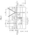
- FIG. 3 is a cross-sectional view of an organic light emitting display device according to an embodiment of the present invention and schematically illustrates one cross-sectional surface of the display area DA illustrated in FIG. 2 .
- a plurality of pixels included in the organic light emitting display device includes a first emissive area EA1, a reflective area RA, and a second emissive area EA2.
- the first emissive area EA1 corresponds to an area which emits light in a first surface direction D1 toward a first surface of a substrate
- the reflective area RA corresponds to an area which reflects light, which is incident on the substrate, in the first surface direction D1 of the substrate
- the second emissive area EA2 corresponds to an area which overlaps the reflective area RA and emits light in a second surface direction D2 toward a second surface opposite to the first surface of the substrate.
- the first surface direction D1 may correspond to a direction from a pixel electrode AE to a common electrode CE, and the second surface direction D2 may be opposite thereto. A structure of each of the areas will be described below.
- the first emissive area EA1 corresponds to an area which emits light in a first surface direction D 1 toward a first surface of the device
- the reflective area RA corresponds to an area which reflects light, which is incident on the device, in the first surface direction D1 of the device.
- the second emissive area EA 2 corresponds to an area which overlaps the reflective area RA and emits light in a second surface direction D2 toward a second surface opposite to the first surface of the device.
- the organic light emitting display device realizes a double-sided device which provides light to both surfaces through the first emissive area EA1 and the second emissive area EA2. Accordingly, the double-sided device may be manufactured without damaging an organic material, and a bidirectional screen having high luminance may be implemented with low power.
- the organic light emitting display device includes a substrate 110, a TFT T, an optional passivation layer 130, a optional intermediate metal 135, an optional planarization layer 140, an organic light emitting device 150, an optional bank 160, an encapsulation layer 170, a black matrix 180, an optional color filter 185, an optional filler 190, and an optional encapsulation substrate 195.
- the substrate 110 may each be a glass substrate or a flexible plastic substrate.
- the substrate 110 may be a sheet or a film which includes cellulose resin such as triacetyl cellulose (TAC), diacetyl cellulose (DAC), or the like, cyclo olefin polymer (COP) such as norbornene derivatives or the like, acryl resin such as cyclo olefin copolymer (COC), poly(methylmethacrylate) (PMMA), or the like, polyolefin such as polycarbonate (PC), polyethylene (PE), polypropylene (PP), or the like, polyester such as polyvinyl alcohol (PVA), poly ether sulfone (PES), polyetheretherketone (PEEK), polyetherimide (PEI), polyethylenenaphthalate (PEN), polyethyleneterephthalate (PET), or the like, polyimide (PI), polysulfone (PSF), fluoride resin, and/or the like, but is not limited thereto.
- a buffer layer 115 may be further provided on the substrate 110.
- the buffer layer 115 may be provided all over an upper surface of the substrate 110.
- the buffer layer 115 prevents water from penetrating into the display panel 100.
- the buffer layer 115 may be formed of an inorganic insulating material, for example, silicon dioxide (SiO 2 ), silicon nitride (SiNx), or a multilayer thereof, but is not limited thereto.
- the TFT T is provided on the substrate 110.
- the TFT T includes an active layer ACT, a gate insulation layer GI, a gate electrode GE, an interlayer dielectric 120, a drain electrode DE, and a source electrode SE.
- the active layer ACT is provided on the substrate 110.
- the active layer ACT may be disposed to overlap the gate electrode GE.
- the active layer ACT may include a drain area disposed in the drain electrode DE side, a source area in the source electrode SE side, and a channel area disposed between the drain area and the source area.
- the channel area may include a semiconductor material on which a dopant is not doped, and the drain area and the source area may each include a semiconductor material with a dopant doped thereon.
- the gate insulation layer GI may be provided on the active layer ACT.
- the gate insulation layer GI may insulate the active layer ACT from the gate electrode GE.
- the gate insulation layer GI may be provided to cover the active layer ACT.
- the gate insulation layer GI may be formed of an inorganic insulating material, for example, silicon dioxide (SiO 2 ), silicon nitride (SiNx), or a multilayer thereof, but is not limited thereto.
- the gate electrode GE may be provided on the gate insulation layer GI.
- the gate electrode GE may overlap the channel area of the active layer ACT with the gate insulation layer GI therebetween.
- the gate electrode GE may be a single layer or a multilayer including, for example, one of molybdenum (Mo), aluminum (Al), chromium (Cr), gold (Au), titanium (Ti), nickel (Ni), neodymium (Nd), and copper (Cu) or an alloy thereof, but is not limited thereto.
- the interlayer dielectric 120 may be provided on the gate electrode GE.
- the interlayer dielectric 120 may insulate the gate electrode GE from the drain electrode DE or the source electrode SE.
- the interlayer dielectric 120 may be formed of an inorganic insulating material (for example, silicon dioxide (SiO 2 ), silicon nitride (SiNx), or a multilayer thereof) which is the same as that of the gate insulation layer GI, but is not limited thereto.
- the source electrode SE and the drain electrode DE may be disposed on the interlayer dielectric 120 and may be spaced apart from each other.
- a first contact hole CNT1, exposing a portion of the drain area of the active layer ACT, and a second contact hole CNT2 which exposes a portion of the source area of the active layer ACT may be provided in the gate insulation layer GI and the interlayer dielectric 120.
- the drain electrode DE may be connected to the drain area of the active layer ACT through the first contact hole CNT1
- the source electrode SE may be connected to the source area of the active layer ACT through the second contact hole CNT2.
- a configuration of the TFT T is not limited to the above-described embodiment and may be variously modified into a configuration capable of being easily realized by those skilled in the art.
- the passivation layer 130 may be provided on the interlayer dielectric 120.
- the passivation layer 130 may insulate the source electrode SE of the TFT T from the intermediate metal 135 and may protect the TFT T.
- the passivation layer 130 may be formed of an inorganic insulating material (for example, silicon dioxide (SiO 2 ), silicon nitride (SiNx), or a multilayer thereof) which is the same as that of the interlayer dielectric 120, but is not limited thereto.
- the intermediate metal 135 may be provided on the passivation layer 130 in order for an electrical connection to be easily made between the source electrode SE of the TFT T and the pixel electrode AE of the organic light emitting device 150.
- the intermediate metal 135 may be connected to the source electrode SE of the TFT T through a third contact hole CNT3. If the intermediate metal 135 is provided, a contact hole is not deeply provided, and thus, a problem of an electrical disconnection is solved.
- the planarization layer 140 may be provided on the substrate 110 to cover the TFT T.
- the planarization layer 140 may protect the TFT T and may planarize an upper surface of the substrate 110 on which the TFT T is provided.
- the planarization layer 140 may be formed of an organic insulating material, for example, acryl resin, epoxy resin, phenolic resin, polyamides resin, polyimides resin, and/or the like, but is not limited thereto.
- An inorganic insulation layer may be additionally provided between the TFT T and the planarization layer 140 according to an embodiment.
- the inorganic insulation layer may protect the TFT T.
- the inorganic insulation layer may be formed of an inorganic insulating material (for example, silicon dioxide (SiO 2 ), silicon nitride (SiNx), or a multilayer thereof) which is the same as that of the gate insulation layer GI, but is not limited thereto.
- a fourth contact hole CNT4 exposing the intermediate metal 135 may be provided in the planarization layer 140 according to an embodiment.
- the intermediate metal 135 may be electrically connected to the pixel electrode AE of the organic light emitting device 150 through the fourth contact hole CNT4, and the source electrode SE of the TFT T may be connected to the pixel electrode AE of the organic light emitting device 150 through the intermediate metal 135.
- the organic light emitting device 150 is provided which may be on the optional planarization layer 140.
- the organic light emitting device 150 includes the pixel electrode AE, an organic light emitting layer EL, and the common electrode CE.
- the pixel electrode AE may be provided on the planarization layer 140.
- the pixel electrode AE may be connected to the source electrode SE of the TFT T through the fourth contact hole CNT4 which is provided in the planarization layer 140.
- the pixel electrode AE may correspond to an anode.
- the pixel electrode AE may be supplied with a hole through the source electrode SE of the TFT T and may inject the hole into the organic light emitting layer EL.
- the pixel electrode AE may include a first pixel electrode pattern AE1 and a second pixel electrode pattern AE2.
- the first pixel electrode pattern AE1 may be provided in the first emissive area EA1 and may include a reflective material for allow light emitted from the organic light emitting layer EL to travel in the first surface direction D1.
- the first pixel electrode pattern AE1 may have a thickness of about 51 nm to 100 nm so as to reflect all of light and may be formed of aluminum (Al), silver (Ag), and/or the like.
- the second pixel electrode pattern AE2 may be provided in the second emissive area EA2 and may include a transparent material for allowing the light emitted from the organic light emitting layer EL to travel in the second surface direction D2.
- the second pixel electrode pattern AE2 may be formed of indium tin oxide (ITO), indium zinc oxide (IZO), and/or the like and may not reflect the light emitted from the organic light emitting layer EL but may transmit the light to allow the light to travel in the second surface direction D2.
- the organic light emitting layer EL is provided on the pixel electrode AE and the bank 160.
- the organic light emitting layer EL may include a hole transporting layer, a light emitting layer, and an electron transporting layer. Furthermore, the organic light emitting layer EL may further include one or more function layers for enhancing the emission efficiency and/or lifetime of the light emitting layer.
- the common electrode CE is provided on the organic light emitting layer EL.
- a hole and an electron may respectively move to the organic light emitting layer EL through the hole transporting layer and the electron transporting layer and may be combined with each other to emit light in the organic light emitting layer EL.
- the common electrode CE may be divided into a first common electrode pattern CE1 and a second common electrode pattern CE2.
- the first common electrode pattern CE1 may be provided in the first emissive area EA1 and may include a transparent material for allowing the light emitted from the organic light emitting layer EL to travel in the first surface direction D1.
- the first common electrode pattern CE1 may be formed of indium tin oxide (ITO), indium zinc oxide (IZO), and/or the like and may not reflect the light emitted from the organic light emitting layer EL but may transmit the light to transfer the light to the outside.
- the second common electrode pattern CE2 may be provided in the reflective area RA and may include a reflective material for allowing the light emitted from the organic light emitting layer EL to travel in the second surface direction D2.
- the second common electrode pattern CE2 may have a thickness of about 51 nm to 100 nm so as to reflect all of light and may be formed of aluminum (Al), silver (Ag), and/or the like.
- the second common electrode pattern CE2 may reflect the light emitted from the organic light emitting layer EL to allow the light to travel in the second surface direction D2. Also, the second common electrode pattern CE2 may reflect external light to perform a mirror function.
- the bank 160 may be provided between adjacent pixel electrodes AE and may define an opening area.
- the bank 160 may include an organic material such as benzocyclobutadiene, acryl, polyimide, or the like. Additionally, the bank 160 may be formed of a photosensitive agent including a black pigment, and in this case, the bank 160 may act as a light blocking member (or a black matrix).
- the encapsulation layer 170 is provided on the organic light emitting device 150.
- the encapsulation layer 170 is provided on the common electrode CE.
- the encapsulation layer 170 may be provided to contact the filler 190.
- the encapsulation layer 170 formed and may prevent water from penetrating into each pixel and for protecting the organic light emitting device 150 vulnerable to external water or oxygen.
- the encapsulation layer 170 according to an embodiment may be formed of an inorganic layer or an organic layer, or may be formed in a multi-layer structure where an inorganic layer and an organic layer are alternately stacked.
- the encapsulation layer 170 may include a first inorganic layer, an organic layer covering the first inorganic layer, and a second inorganic layer covering the organic layer, which are provided on the substrate 110.
- the first inorganic layer may be disposed closest to the organic light emitting device 150 and may be formed of an inorganic insulating material, which enables low temperature deposition to be performed, such as nitride silicon (SiNx), oxide silicon (SiOx), oxynitride silicon (SiON), oxide aluminum (AlxOy), or the like.
- the organic layer may be provided on the substrate 110 to cover a whole portion of the first inorganic layer.
- the organic layer decreases a stress between layers caused by the bending of the display device and reinforces planarization performance.
- the organic layer according to an embodiment may include an organic insulating material such as benzocyclobutadiene, acryl, polyimide, or the like.
- the second inorganic layer may be provided on the substrate 110 to cover a whole portion of the organic layer and each of side surfaces of the first inorganic layer.
- the second inorganic layer primarily prevents external water or oxygen from penetrating into the organic layer and the first inorganic layer.
- the second inorganic layer according to an embodiment may be formed of an inorganic insulating material, which enables low temperature deposition to be performed, such as nitride silicon (SiNx), oxide silicon (SiOx), oxynitride silicon (SiON), oxide aluminum (AlxOy), or the like, or may be formed of a material which is the same as that of the first inorganic layer.
- the black matrix 180 defines an opening area of each pixel provided on the substrate 110. That is, the black matrix 180 is provided on the encapsulation substrate 195 overlapping a light blocking area other than an opening area overlapping the organic light emitting device 150 of each pixel, thereby preventing color mixture between adjacent opening areas.
- the black matrix 180 according to the invention includes a plurality of first light blocking patterns which cover the plurality of gate lines and the pixel circuits of the pixels, a plurality of second light blocking patterns which cover the plurality of data lines and a plurality of pixel driving power lines, and a third light blocking pattern which covers an edge of the encapsulation layer 170.
- the color filter 185 may be directly formed on a top of the encapsulation layer 170 overlapping the opening area defined by the black matrix 180 and may be provided on the encapsulation layer 170 in the first emissive area EA1.
- the organic light emitting device 150 may correspond to a white organic light emitting device, and thus, the color filter 185 may transmit only light, having a wavelength of a color corresponding to a corresponding pixel, of white light.
- the color filter 185 may include a red color filter, a green color filter, and a blue color filter respectively corresponding to colors defined in a plurality of pixels.
- the organic light emitting display device includes the color filter 185, a related art polarizer (for example, a circular polarizer) for preventing dazzle may be removed, and thus, a light transmittance and a color reproduction rate of each pixel are enhanced.
- a related art polarizer for example, a circular polarizer
- the filler 190 may be provided on the encapsulation layer 170.
- the filler 190 may contact the encapsulation layer 170.
- the filler 190 protects the TFT T, the organic light emitting device 150, etc., from an external impact.
- the filler 190 may perform a function of bonding the substrate 110 to the encapsulation substrate 195.
- the filler 190 may be formed of acrylic or epoxy-based resin having a good visible light transmittance, for example, a visible light transmittance of 90% or more.
- the encapsulation substrate 195 may be provided on the organic light emitting device 150 and the encapsulation layer 170.
- the encapsulation substrate 195 may be provided on a whole surface.
- the encapsulation substrate 195 may be an encapsulation substrate.
- the encapsulation substrate 195 prevents water from penetrating into the display panel 100. Also, the encapsulation substrate 195 protects the organic light emitting device 150 and the TFT T, which are included in the display panel 100, from an external impact.
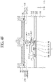
- FIGS. 4A to 4G are cross-sectional views for describing a method of manufacturing an organic light emitting display device according to an embodiment of the present invention. Therefore, like reference numerals refer to like elements, and repetitive descriptions of a material and a structure of each element are omitted.
- an optional buffer layer 115, a TFT T, an optional passivation layer 130, an optional intermediate metal 135, an optional planarization layer 140, and an optional fourth contact hole CNT4 are sequentially formed on a substrate 110. These are made by any deposition, mask and etch process of those known in the art and, thus, each step is not described in detail.
- a first pixel electrode pattern AE1 connected to the intermediate metal 135 through the fourth contact hole CNT4 may be formed in a first emissive area EA1.
- the first pixel electrode pattern AE1 may have a thickness of about 51 nm to 100 nm so as to reflect all of light and may be formed of a reflective material.
- the reflective material may be aluminum (Al) or silver (Ag), but is not limited thereto.
- Layer AE1 is formed by any acceptable known deposition and etch process.
- a second pixel electrode pattern AE2 contacting the first pixel electrode pattern AE1 may be formed on the same layer as the first pixel electrode pattern AE1 in a second emissive area EA2.
- the second pixel electrode pattern AE2 may be formed of a transparent material so as to transmit light.
- the transparent material may be ITO or IZO, but is not limited thereto.
- Layer AE2 is formed by any acceptable known deposition and etch process.
- a bank 160 and an organic light emitting layer EL may be formed on the first and second pixel electrode patterns AE1 and AE2.
- the bank 160 may be formed between the first and second pixel electrode patterns AE1 and AE2 or between adjacent pixel electrodes AE to define an opening area.
- a first common electrode pattern CE1 is formed in the first emissive area EA1.
- the first common electrode pattern CE1 may be formed of a transparent material so as to transmit light.
- the transparent material may be ITO or IZO, but is not limited thereto.
- a second common electrode pattern CE2 contacting the first common electrode pattern CE1 is formed on the same layer as the first common electrode pattern CE1 in a reflective area RA.
- the second common electrode pattern CE2 may have a thickness of about 51 nm to 100 nm so as to reflect all of light and may be formed of a reflective material.
- the reflective material may be aluminum (Al) or silver (Ag), but is not limited thereto.
- an encapsulation layer 170, a black matrix 180, an optional color filter 185, an optional filler 190, and an optional encapsulation substrate 195 are sequentially formed on the first and second common electrode patterns CE1 and CE2.
- the first and second pixel electrode patterns AE1 and AE2 may configure a pixel electrode AE
- the first and second common electrode patterns CE1 and CE2 configure a common electrode CE.
- first pixel electrode pattern AE1 is provided in the first emissive area EA1 and is formed of the reflective material, light emitted from an organic light emitting layer EL may travel in a first surface direction D1
- second pixel electrode pattern AE2 is provided in the second emissive area EA2 and is formed of the transparent material, the light emitted from the organic light emitting layer EL may travel in a second surface direction D2.
- the first common electrode pattern CE1 is provided in the first emissive area EA1 and is formed of the transparent material, the light emitted from the organic light emitting layer EL may travel in the first surface direction D1
- the second common electrode pattern CE2 is provided in the second emissive area EA2 and is formed of the reflective material, the light emitted from the organic light emitting layer EL may travel in the second surface direction D2.
- the first pixel electrode pattern AE1, the second pixel electrode pattern AE2, the first common electrode pattern CE1, and the second common electrode pattern CE2 may each be formed of different materials through incremental processes at different times, and thus, may be provided in different areas to perform different functions.
- a common light emitting layer EL and a common drive transistor T can therefore provide light that is emitted from both the first surface D1 and the second D2. Since the very same transistor T and the same light emitting layer EL are used for both light emissions, it can be assured that the light emitted will be at the same time and have approximately the same amplitude from both surfaces. In most embodiments, the light emitted from both surfaces will pass through the color filters of the same type and thus be of the same color as well, but this is not required.
- the display on both sides can be made nearly identical.
- material and thickness of AE2 the same as that for CE1 both light sources will pass through the same material and thickness of their respective transparent electrodes.
- the substrate 110 and various layers 115, 120 and 130 on side D2 to have approximately the same optical properties as layers 170, 190 and 195, on the side D1
- the intensity, color and other properties of the light emitted at from that particular pixel at that location on each side can be made approximately the same.
- the organic light emitting display device according to the present embodiment may realize bidirectional image display.
- an order in which the pixel electrode AE and the common electrode CE are formed may switch therebetween.
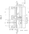
- FIG. 5 is a cross-sectional view of an organic light emitting display device according to an embodiment of the present invention and illustrates an example where an auxiliary color filter is added to the organic light emitting display device illustrated in FIG. 3 .
- an auxiliary color filter is added to the organic light emitting display device illustrated in FIG. 3 .
- the organic light emitting display device may further include an auxiliary color filter 185a.
- the auxiliary color filter 185a may be provided in a second emissive area EA2. That is, the auxiliary color filter 185a according to an embodiment may be provided on an interlayer dielectric 120 provided in the second emissive area EA2.
- the auxiliary color filter 185a according to an embodiment may be inserted into a planarization layer 140 provided in the second emissive area EA2, and in this case, the planarization layer 140 may have a two-layered structure where two layers are stacked with the auxiliary color filter 185a therebetween.
- the planarization layer 140 may include a first planarization layer covering a TFT T and a second planarization layer covering the auxiliary color filter 185a provided on the first planarization layer.
- the auxiliary color filter 185a may transmit light of any color. It can have a wavelength of a color corresponding to a corresponding particular pixel or subpixel color, whether red, blue or green.. It can also provide white light. The light is emitted in a second surface direction D2 from an organic light emitting layer EL provided in the second emissive area EA2, thereby allowing a color image to be displayed in the second surface direction D2 of the substrate 110.
- the auxiliary color filter 185a may be formed of a material which is the same as that of the color filter 185 provided in a first emissive area EA1 if it is desired to provide exactly the same color in both directions.
- the organic light emitting display device includes the auxiliary color filter 185a, a color image that is output from surface D2 is approximately the exact same in both timing, color, amplitude, brightness and other factors as that out of surface D1 may be displayed in the second surface direction D2 of the substrate 110.
- the light emitting device can have a large display area DA that includes many thousands of pixels and subpixels identical to that shown in Fig. 3 .
- the organic light emitting display device since the polarizer is replaced with the color filter, a light transmittance and a color reproduction rate are enhanced, and bidirectional image display is realized through the second emissive area.
Claims (15)
- Dispositif d'affichage électroluminescent organique ayant une première surface et une deuxième surface, le dispositif d'affichage électroluminescent organique comprenant :un substrat (110) ;une pluralité de pixels sur le substrat (110), la pluralité de pixels comportant chacun :une première zone émissive (EA1) configurée pour émettre de la lumière dans une direction de première surface (D1) ;une zone réfléchissante (RA) configurée pour réfléchir la lumière incidente dans la direction de première surface (D1) ;une matrice noire (180) disposée entre la première zone émissive et la zone réfléchissante et définissant une zone d'ouverture de chaque pixel disposé sur le substrat (110) ;une couche d'encapsulation (170) recouvrant une électrode commune (CE) disposée sur la couche électroluminescente organique ; etune deuxième zone émissive (EA2) chevauchant la zone réfléchissante (RA) et configurée pour émettre de la lumière dans une direction de deuxième surface (D2) à l'opposé de la direction de première surface (D1) ;dans lequel la matrice noire comporte une pluralité de premiers motifs bloquant la lumière qui recouvrent une pluralité de lignes de grille et un circuit de pixel de chaque pixel, une pluralité de deuxièmes motifs bloquant la lumière qui recouvrent une pluralité de lignes de données et une pluralité de lignes d'alimentation de commande de pixel, et un troisième motif bloquant la lumière qui recouvre un bord de la couche d'encapsulation (170) .
- Dispositif d'affichage électroluminescent organique de la revendication 1, dans lequel la pluralité de pixels comprennent chacun :le circuit de pixel comportant un transistor en couches minces disposé dans la première zone émissive (EA1) ;une électrode de pixel (AE) connectée au transistor en couches minces et disposée dans la première zone émissive (EA1) et la deuxième zone émissive (EA2) ; etune couche électroluminescente organique disposée sur l'électrode de pixel.
- Dispositif d'affichage électroluminescent organique de la revendication 2, dans lequel l'électrode de pixel (AE) comprend :un premier motif d'électrode de pixel (AE1) connecté au transistor en couches minces et disposé dans la première zone émissive, le premier motif d'électrode de pixel comportant un matériau réfléchissant ; etun deuxième motif d'électrode de pixel (AE2) connecté électriquement au premier motif d'électrode de pixel (AE1) et disposé dans la zone réfléchissante (RA), le deuxième motif d'électrode de pixel (AE2) comportant un matériau transparent.
- Dispositif d'affichage électroluminescent organique de la revendication 3, comprenant en outre : un talus (160) recouvrant une partie de connexion entre le premier motif d'électrode de pixel (AE1) et le deuxième motif d'électrode de pixel (AE2).
- Dispositif d'affichage électroluminescent organique de l'une quelconque des revendications 2 à 4, dans lequel l'électrode commune (CE) comprend :un premier motif d'électrode commune (CE1) disposé dans la première zone émissive (EA1), le premier motif d'électrode commune (CE1) comportant un matériau transparent ; etun deuxième motif d'électrode commune (CE2) connecté électriquement au premier motif d'électrode commune (CE1) et disposé dans la zone réfléchissante (RA), le deuxième motif d'électrode commune (CE2) comportant un matériau réfléchissant.
- Dispositif d'affichage électroluminescent organique de l'une quelconque des revendications 2 à 5, dans lequel la couche d'encapsulation (170) recouvre l'électrode commune (CE) de chacun de la pluralité de pixels ; et le dispositif d'affichage électroluminescent organique comprend en outreun filtre coloré dans la première zone émissive ;un matériau de remplissage (190) recouvrant le filtre coloré (185) et la zone réfléchissante (RA) ; etun substrat d'encapsulation (195) attaché sur le matériau de remplissage,dans lequel la couche électroluminescente organique de chacun de la pluralité de pixels émet de la lumière blanche.
- Dispositif d'affichage électroluminescent organique de l'une quelconque des revendications 1 à 5, comprenant en outre : un filtre coloré dans la première zone émissive,
dans lequel la couche électroluminescente organique de chacun de la pluralité de pixels émet de la lumière blanche. - Dispositif d'affichage électroluminescent organique de la revendication 6 ou la revendication 7, comprenant en outre un filtre coloré auxiliaire dans la deuxième zone émissive.
- Dispositif d'affichage électroluminescent organique de la revendication 1 comprenant en outre :un transistor positionné sur le substrat ;une première couche réfléchissant la lumière positionnée pour recouvrir le transistor, le transistor et la première couche réfléchissant la lumière étant positionnés dans la première zone émissive (EA1) ;une deuxième couche réfléchissante, la deuxième couche réfléchissante étant adjacente à la première zone émissive (EA1) et la deuxième couche réfléchissante étant positionnée dans la zone réfléchissante (RA) ;la deuxième zone émissive (EA2) sous-jacente à la deuxième couche réfléchissante ;l'électrode commune (CE) recouvrant à la fois la première et la deuxième zone émissive (EA1/EA2) ;une électrode de commande sous-jacente à la fois à la première et la deuxième zone émissive ; etune ligne de connexion électrique qui s'étend du transistor à l'électrode de commande à la fois pour la première zone émissive (EA1) et la deuxième zone émissive (EA2) .
- Dispositif d'affichage électroluminescent organique de la revendication 9 dans lequel la couche d'encapsulation (170) recouvre les première et deuxième zones émissives (EA1/EA2).
- Dispositif d'affichage électroluminescent organique de la revendication 9 ou 10 comprenant en outre : une couche de matériau de remplissage (190) recouvrant les première et deuxième zones émissives (EA1/EA2).
- Dispositif d'affichage électroluminescent organique de la revendication 11 dans lequel la couche d'encapsulation (170) recouvre la couche de matériau de remplissage (190).
- Dispositif d'affichage électroluminescent organique de la revendication 11 dans lequel la couche d'encapsulation (170) est sous-jacente à la couche de matériau de remplissage (190).
- Dispositif d'affichage électroluminescent organique de l'une quelconque des revendications 9 à 13 dans lequel le substrat (110) est transparent.
- Procédé de formation du dispositif d'affichage électroluminescent selon la revendication 1 comprenant :la formation d'un transistor de commande sur un substrat ;la formation d'une première électrode réfléchissant la lumière recouvrant le transistor de commande ;la formation d'une première électrode transparente à la lumière adjacente à la première électrode réfléchissant la lumière et approximativement dans le même plan que la première électrode réfléchissant la lumière ;la formation d'une connexion électrique commune allant du transistor de commande à la première électrode réfléchissant la lumière et à la première électrode transparente à la lumière ;la formation d'une seule couche photoémissive qui recouvre à la fois la première électrode réfléchissant la lumière et la première électrode transparente à la lumière ;la formation d'une deuxième électrode réfléchissant la lumière recouvrant la première électrode transparente à la lumière ;la formation d'une deuxième électrode transparente à la lumière recouvrant la première électrode réfléchissant la lumière ; etla formation de la matrice noire avec au moins un motif bloquant la lumière entre la deuxième électrode réfléchissant la lumière et la deuxième électrode transparente à la lumière.
Applications Claiming Priority (1)
| Application Number | Priority Date | Filing Date | Title |
|---|---|---|---|
| KR1020160182423A KR20180077758A (ko) | 2016-12-29 | 2016-12-29 | 유기 발광 표시 장치 |
Publications (2)
| Publication Number | Publication Date |
|---|---|
| EP3343628A1 EP3343628A1 (fr) | 2018-07-04 |
| EP3343628B1 true EP3343628B1 (fr) | 2023-01-04 |
Family
ID=60569693
Family Applications (1)
| Application Number | Title | Priority Date | Filing Date |
|---|---|---|---|
| EP17204735.9A Active EP3343628B1 (fr) | 2016-12-29 | 2017-11-30 | Dispositif électroluminescent organique d'affichage d'image et son procédé de fabrication |
Country Status (4)
| Country | Link |
|---|---|
| US (1) | US10903297B2 (fr) |
| EP (1) | EP3343628B1 (fr) |
| KR (1) | KR20180077758A (fr) |
| CN (1) | CN108258014B (fr) |
Families Citing this family (11)
| Publication number | Priority date | Publication date | Assignee | Title |
|---|---|---|---|---|
| KR102651733B1 (ko) * | 2018-12-20 | 2024-03-28 | 엘지디스플레이 주식회사 | 표시장치 |
| CN109713018B (zh) * | 2019-01-14 | 2020-08-21 | 京东方科技集团股份有限公司 | 一种显示装置及其制作方法 |
| CN110190094B (zh) * | 2019-05-22 | 2022-05-03 | 武汉华星光电半导体显示技术有限公司 | 一种显示面板及其制作方法、智能终端 |
| CN110350016B (zh) | 2019-07-24 | 2022-04-29 | 京东方科技集团股份有限公司 | 显示装置及显示控制方法 |
| CN110729328B (zh) * | 2019-09-17 | 2022-03-08 | 武汉华星光电半导体显示技术有限公司 | 有机发光二极管显示面板及有机发光二极管显示装置 |
| CN111063711A (zh) * | 2019-12-10 | 2020-04-24 | 深圳市华星光电半导体显示技术有限公司 | 双面显示面板及其制备方法 |
| KR20210085135A (ko) | 2019-12-30 | 2021-07-08 | 엘지디스플레이 주식회사 | 투명 표시 장치 |
| CN111430414A (zh) * | 2020-03-31 | 2020-07-17 | 京东方科技集团股份有限公司 | Oled显示面板及制备方法、显示装置 |
| US11152538B1 (en) * | 2020-04-03 | 2021-10-19 | Sharp Kabushiki Kaisha | High on-axis brightness and low color shift QD-LED pixel |
| US20210359285A1 (en) * | 2020-05-18 | 2021-11-18 | Wuhan China Star Optoelectronics Semiconductor Display Technology Co., Ltd. | Display panel and manufacturing method thereof |
| CN116367636B (zh) * | 2023-05-10 | 2023-08-11 | 惠科股份有限公司 | 像素结构、显示面板及显示面板制备方法 |
Citations (2)
| Publication number | Priority date | Publication date | Assignee | Title |
|---|---|---|---|---|
| EP1585175A2 (fr) * | 2004-04-07 | 2005-10-12 | Sel Semiconductor Energy Laboratory Co., Ltd. | Dispositif électroluminescent, dispositif électronique et dispositif de télévision |
| US20120097928A1 (en) * | 2010-10-22 | 2012-04-26 | Tae-Gon Kim | Organic light emitting diode display |
Family Cites Families (19)
| Publication number | Priority date | Publication date | Assignee | Title |
|---|---|---|---|---|
| AU2003262928A1 (en) * | 2002-08-28 | 2004-03-19 | Dr. Reddy's Laboratories Limited | Crystalline form of nateglinide and process for preparation thereof |
| AU2003289446A1 (en) * | 2002-12-27 | 2004-07-29 | Semiconductor Energy Laboratory Co., Ltd. | Display device |
| US7566902B2 (en) * | 2003-05-16 | 2009-07-28 | Semiconductor Energy Laboratory Co., Ltd. | Light-emitting device and electronic device |
| KR100581913B1 (ko) * | 2004-05-22 | 2006-05-23 | 삼성에스디아이 주식회사 | 유기 전계 발광 표시장치 |
| KR100617193B1 (ko) * | 2004-06-03 | 2006-08-31 | 엘지전자 주식회사 | 양방향 유기 el 디스플레이 소자 및 그 제조 방법 |
| US7420324B2 (en) | 2004-06-03 | 2008-09-02 | Lg Display Co., Ltd. | Organic EL display and fabricating method thereof |
| US20060038752A1 (en) * | 2004-08-20 | 2006-02-23 | Eastman Kodak Company | Emission display |
| JP4289332B2 (ja) * | 2004-09-30 | 2009-07-01 | セイコーエプソン株式会社 | El表示装置、el表示装置の製造方法、及び電子機器 |
| KR100726645B1 (ko) | 2005-10-14 | 2007-06-11 | 엘지전자 주식회사 | 전계 발광소자 및 이의 제조방법 |
| KR100645707B1 (ko) * | 2006-01-27 | 2006-11-15 | 삼성에스디아이 주식회사 | 유기전계발광 표시장치 및 그 제조방법 |
| JP2009054328A (ja) * | 2007-08-24 | 2009-03-12 | Hitachi Displays Ltd | 有機el表示装置 |
| JP5589452B2 (ja) * | 2010-03-11 | 2014-09-17 | セイコーエプソン株式会社 | 発光装置および電子機器、発光装置の駆動方法 |
| TWI478333B (zh) * | 2012-01-30 | 2015-03-21 | Ind Tech Res Inst | 雙面發光顯示面板 |
| JP2015022914A (ja) * | 2013-07-19 | 2015-02-02 | ソニー株式会社 | 表示装置およびその製造方法、並びに電子機器 |
| US9691835B2 (en) * | 2013-12-24 | 2017-06-27 | Boe Technology Group Co., Ltd. | Double-face display panel |
| KR102316092B1 (ko) * | 2014-11-28 | 2021-10-25 | 삼성디스플레이 주식회사 | 표시 패널 및 유기 발광 표시 장치 |
| KR102407674B1 (ko) * | 2014-12-22 | 2022-06-13 | 삼성디스플레이 주식회사 | 발광 표시 장치 |
| JP2018077982A (ja) * | 2016-11-08 | 2018-05-17 | 株式会社ジャパンディスプレイ | 有機el表示装置 |
| KR102611794B1 (ko) * | 2016-11-30 | 2023-12-07 | 엘지디스플레이 주식회사 | 유기발광 표시장치와 그의 제조방법 |
-
2016
- 2016-12-29 KR KR1020160182423A patent/KR20180077758A/ko not_active Application Discontinuation
-
2017
- 2017-11-20 US US15/818,487 patent/US10903297B2/en active Active
- 2017-11-30 EP EP17204735.9A patent/EP3343628B1/fr active Active
- 2017-12-15 CN CN201711353762.XA patent/CN108258014B/zh active Active
Patent Citations (2)
| Publication number | Priority date | Publication date | Assignee | Title |
|---|---|---|---|---|
| EP1585175A2 (fr) * | 2004-04-07 | 2005-10-12 | Sel Semiconductor Energy Laboratory Co., Ltd. | Dispositif électroluminescent, dispositif électronique et dispositif de télévision |
| US20120097928A1 (en) * | 2010-10-22 | 2012-04-26 | Tae-Gon Kim | Organic light emitting diode display |
Also Published As
| Publication number | Publication date |
|---|---|
| US10903297B2 (en) | 2021-01-26 |
| CN108258014A (zh) | 2018-07-06 |
| US20180190748A1 (en) | 2018-07-05 |
| KR20180077758A (ko) | 2018-07-09 |
| EP3343628A1 (fr) | 2018-07-04 |
| CN108258014B (zh) | 2022-04-19 |
Similar Documents
| Publication | Publication Date | Title |
|---|---|---|
| EP3343628B1 (fr) | Dispositif électroluminescent organique d'affichage d'image et son procédé de fabrication | |
| US11398538B2 (en) | Light emitting diode display device and multi-screen display device using the same | |
| US11487143B2 (en) | Display device, multi-screen display device using the same and method for manufacturing the same | |
| US10937815B2 (en) | Light emitting diode display device | |
| US10910441B2 (en) | Organic light emitting display device | |
| EP3316302B1 (fr) | Afficheur à diodes électroluminescentes | |
| US10468396B2 (en) | Display device and multi-screen display device using the same | |
| KR20190006101A (ko) | 발광 장치 및 전자 장치 | |
| KR20230161290A (ko) | 표시 장치 및 표시 장치의 제조 방법 | |
| CN117238921A (zh) | 显示装置 | |
| KR20210066285A (ko) | 표시 장치 | |
| CN115295571A (zh) | 显示装置 | |
| KR20170125485A (ko) | 유기발광 표시장치 및 그의 제조방법 |
Legal Events
| Date | Code | Title | Description |
|---|---|---|---|
| PUAI | Public reference made under article 153(3) epc to a published international application that has entered the european phase |
Free format text: ORIGINAL CODE: 0009012 |
|
| STAA | Information on the status of an ep patent application or granted ep patent |
Free format text: STATUS: REQUEST FOR EXAMINATION WAS MADE |
|
| 17P | Request for examination filed |
Effective date: 20171130 |
|
| AK | Designated contracting states |
Kind code of ref document: A1 Designated state(s): AL AT BE BG CH CY CZ DE DK EE ES FI FR GB GR HR HU IE IS IT LI LT LU LV MC MK MT NL NO PL PT RO RS SE SI SK SM TR |
|
| AX | Request for extension of the european patent |
Extension state: BA ME |
|
| RBV | Designated contracting states (corrected) |
Designated state(s): AL AT BE BG CH CY CZ DE DK EE ES FI FR GB GR HR HU IE IS IT LI LT LU LV MC MK MT NL NO PL PT RO RS SE SI SK SM TR |
|
| STAA | Information on the status of an ep patent application or granted ep patent |
Free format text: STATUS: EXAMINATION IS IN PROGRESS |
|
| 17Q | First examination report despatched |
Effective date: 20210602 |
|
| STAA | Information on the status of an ep patent application or granted ep patent |
Free format text: STATUS: EXAMINATION IS IN PROGRESS |
|
| GRAP | Despatch of communication of intention to grant a patent |
Free format text: ORIGINAL CODE: EPIDOSNIGR1 |
|
| STAA | Information on the status of an ep patent application or granted ep patent |
Free format text: STATUS: GRANT OF PATENT IS INTENDED |
|
| INTG | Intention to grant announced |
Effective date: 20220713 |
|
| GRAS | Grant fee paid |
Free format text: ORIGINAL CODE: EPIDOSNIGR3 |
|
| GRAA | (expected) grant |
Free format text: ORIGINAL CODE: 0009210 |
|
| STAA | Information on the status of an ep patent application or granted ep patent |
Free format text: STATUS: THE PATENT HAS BEEN GRANTED |
|
| AK | Designated contracting states |
Kind code of ref document: B1 Designated state(s): AL AT BE BG CH CY CZ DE DK EE ES FI FR GB GR HR HU IE IS IT LI LT LU LV MC MK MT NL NO PL PT RO RS SE SI SK SM TR |
|
| REG | Reference to a national code |
Ref country code: GB Ref legal event code: FG4D |
|
| REG | Reference to a national code |
Ref country code: CH Ref legal event code: EP |
|
| REG | Reference to a national code |
Ref country code: AT Ref legal event code: REF Ref document number: 1542563 Country of ref document: AT Kind code of ref document: T Effective date: 20230115 |
|
| REG | Reference to a national code |
Ref country code: DE Ref legal event code: R096 Ref document number: 602017065179 Country of ref document: DE |
|
| REG | Reference to a national code |
Ref country code: IE Ref legal event code: FG4D |
|
| REG | Reference to a national code |
Ref country code: LT Ref legal event code: MG9D |
|
| REG | Reference to a national code |
Ref country code: NL Ref legal event code: MP Effective date: 20230104 |
|
| REG | Reference to a national code |
Ref country code: AT Ref legal event code: MK05 Ref document number: 1542563 Country of ref document: AT Kind code of ref document: T Effective date: 20230104 |
|
| PG25 | Lapsed in a contracting state [announced via postgrant information from national office to epo] |
Ref country code: NL Free format text: LAPSE BECAUSE OF FAILURE TO SUBMIT A TRANSLATION OF THE DESCRIPTION OR TO PAY THE FEE WITHIN THE PRESCRIBED TIME-LIMIT Effective date: 20230104 |
|
| PG25 | Lapsed in a contracting state [announced via postgrant information from national office to epo] |
Ref country code: RS Free format text: LAPSE BECAUSE OF FAILURE TO SUBMIT A TRANSLATION OF THE DESCRIPTION OR TO PAY THE FEE WITHIN THE PRESCRIBED TIME-LIMIT Effective date: 20230104 Ref country code: PT Free format text: LAPSE BECAUSE OF FAILURE TO SUBMIT A TRANSLATION OF THE DESCRIPTION OR TO PAY THE FEE WITHIN THE PRESCRIBED TIME-LIMIT Effective date: 20230504 Ref country code: NO Free format text: LAPSE BECAUSE OF FAILURE TO SUBMIT A TRANSLATION OF THE DESCRIPTION OR TO PAY THE FEE WITHIN THE PRESCRIBED TIME-LIMIT Effective date: 20230404 Ref country code: LV Free format text: LAPSE BECAUSE OF FAILURE TO SUBMIT A TRANSLATION OF THE DESCRIPTION OR TO PAY THE FEE WITHIN THE PRESCRIBED TIME-LIMIT Effective date: 20230104 Ref country code: LT Free format text: LAPSE BECAUSE OF FAILURE TO SUBMIT A TRANSLATION OF THE DESCRIPTION OR TO PAY THE FEE WITHIN THE PRESCRIBED TIME-LIMIT Effective date: 20230104 Ref country code: HR Free format text: LAPSE BECAUSE OF FAILURE TO SUBMIT A TRANSLATION OF THE DESCRIPTION OR TO PAY THE FEE WITHIN THE PRESCRIBED TIME-LIMIT Effective date: 20230104 Ref country code: ES Free format text: LAPSE BECAUSE OF FAILURE TO SUBMIT A TRANSLATION OF THE DESCRIPTION OR TO PAY THE FEE WITHIN THE PRESCRIBED TIME-LIMIT Effective date: 20230104 Ref country code: AT Free format text: LAPSE BECAUSE OF FAILURE TO SUBMIT A TRANSLATION OF THE DESCRIPTION OR TO PAY THE FEE WITHIN THE PRESCRIBED TIME-LIMIT Effective date: 20230104 |
|
| PG25 | Lapsed in a contracting state [announced via postgrant information from national office to epo] |
Ref country code: SE Free format text: LAPSE BECAUSE OF FAILURE TO SUBMIT A TRANSLATION OF THE DESCRIPTION OR TO PAY THE FEE WITHIN THE PRESCRIBED TIME-LIMIT Effective date: 20230104 Ref country code: PL Free format text: LAPSE BECAUSE OF FAILURE TO SUBMIT A TRANSLATION OF THE DESCRIPTION OR TO PAY THE FEE WITHIN THE PRESCRIBED TIME-LIMIT Effective date: 20230104 Ref country code: IS Free format text: LAPSE BECAUSE OF FAILURE TO SUBMIT A TRANSLATION OF THE DESCRIPTION OR TO PAY THE FEE WITHIN THE PRESCRIBED TIME-LIMIT Effective date: 20230504 Ref country code: GR Free format text: LAPSE BECAUSE OF FAILURE TO SUBMIT A TRANSLATION OF THE DESCRIPTION OR TO PAY THE FEE WITHIN THE PRESCRIBED TIME-LIMIT Effective date: 20230405 Ref country code: FI Free format text: LAPSE BECAUSE OF FAILURE TO SUBMIT A TRANSLATION OF THE DESCRIPTION OR TO PAY THE FEE WITHIN THE PRESCRIBED TIME-LIMIT Effective date: 20230104 |
|
| REG | Reference to a national code |
Ref country code: DE Ref legal event code: R097 Ref document number: 602017065179 Country of ref document: DE |
|
| PG25 | Lapsed in a contracting state [announced via postgrant information from national office to epo] |
Ref country code: SM Free format text: LAPSE BECAUSE OF FAILURE TO SUBMIT A TRANSLATION OF THE DESCRIPTION OR TO PAY THE FEE WITHIN THE PRESCRIBED TIME-LIMIT Effective date: 20230104 Ref country code: RO Free format text: LAPSE BECAUSE OF FAILURE TO SUBMIT A TRANSLATION OF THE DESCRIPTION OR TO PAY THE FEE WITHIN THE PRESCRIBED TIME-LIMIT Effective date: 20230104 Ref country code: EE Free format text: LAPSE BECAUSE OF FAILURE TO SUBMIT A TRANSLATION OF THE DESCRIPTION OR TO PAY THE FEE WITHIN THE PRESCRIBED TIME-LIMIT Effective date: 20230104 Ref country code: DK Free format text: LAPSE BECAUSE OF FAILURE TO SUBMIT A TRANSLATION OF THE DESCRIPTION OR TO PAY THE FEE WITHIN THE PRESCRIBED TIME-LIMIT Effective date: 20230104 Ref country code: CZ Free format text: LAPSE BECAUSE OF FAILURE TO SUBMIT A TRANSLATION OF THE DESCRIPTION OR TO PAY THE FEE WITHIN THE PRESCRIBED TIME-LIMIT Effective date: 20230104 |
|
| PGFP | Annual fee paid to national office [announced via postgrant information from national office to epo] |
Ref country code: GB Payment date: 20230920 Year of fee payment: 7 |
|
| PLBE | No opposition filed within time limit |
Free format text: ORIGINAL CODE: 0009261 |
|
| STAA | Information on the status of an ep patent application or granted ep patent |
Free format text: STATUS: NO OPPOSITION FILED WITHIN TIME LIMIT |
|
| PG25 | Lapsed in a contracting state [announced via postgrant information from national office to epo] |
Ref country code: SK Free format text: LAPSE BECAUSE OF FAILURE TO SUBMIT A TRANSLATION OF THE DESCRIPTION OR TO PAY THE FEE WITHIN THE PRESCRIBED TIME-LIMIT Effective date: 20230104 |
|
| PGFP | Annual fee paid to national office [announced via postgrant information from national office to epo] |
Ref country code: FR Payment date: 20230922 Year of fee payment: 7 |
|
| 26N | No opposition filed |
Effective date: 20231005 |
|
| PG25 | Lapsed in a contracting state [announced via postgrant information from national office to epo] |
Ref country code: SI Free format text: LAPSE BECAUSE OF FAILURE TO SUBMIT A TRANSLATION OF THE DESCRIPTION OR TO PAY THE FEE WITHIN THE PRESCRIBED TIME-LIMIT Effective date: 20230104 |
|
| PGFP | Annual fee paid to national office [announced via postgrant information from national office to epo] |
Ref country code: DE Payment date: 20230920 Year of fee payment: 7 |