EP3343427A1 - Procédé et dispositif de gestion de la consommation en courant d'un module intégré - Google Patents
Procédé et dispositif de gestion de la consommation en courant d'un module intégré Download PDFInfo
- Publication number
- EP3343427A1 EP3343427A1 EP17186781.5A EP17186781A EP3343427A1 EP 3343427 A1 EP3343427 A1 EP 3343427A1 EP 17186781 A EP17186781 A EP 17186781A EP 3343427 A1 EP3343427 A1 EP 3343427A1
- Authority
- EP
- European Patent Office
- Prior art keywords
- transistor
- terminal
- auxiliary
- coupled
- circuit
- Prior art date
- Legal status (The legal status is an assumption and is not a legal conclusion. Google has not performed a legal analysis and makes no representation as to the accuracy of the status listed.)
- Granted
Links
Images


Classifications
-
- H—ELECTRICITY
- H03—ELECTRONIC CIRCUITRY
- H03K—PULSE TECHNIQUE
- H03K19/00—Logic circuits, i.e. having at least two inputs acting on one output; Inverting circuits
- H03K19/0008—Arrangements for reducing power consumption
- H03K19/0013—Arrangements for reducing power consumption in field effect transistor circuits
-
- G—PHYSICS
- G06—COMPUTING OR CALCULATING; COUNTING
- G06K—GRAPHICAL DATA READING; PRESENTATION OF DATA; RECORD CARRIERS; HANDLING RECORD CARRIERS
- G06K19/00—Record carriers for use with machines and with at least a part designed to carry digital markings
- G06K19/06—Record carriers for use with machines and with at least a part designed to carry digital markings characterised by the kind of the digital marking, e.g. shape, nature, code
- G06K19/067—Record carriers with conductive marks, printed circuits or semiconductor circuit elements, e.g. credit or identity cards also with resonating or responding marks without active components
- G06K19/07—Record carriers with conductive marks, printed circuits or semiconductor circuit elements, e.g. credit or identity cards also with resonating or responding marks without active components with integrated circuit chips
- G06K19/073—Special arrangements for circuits, e.g. for protecting identification code in memory
- G06K19/07309—Means for preventing undesired reading or writing from or onto record carriers
- G06K19/07363—Means for preventing undesired reading or writing from or onto record carriers by preventing analysis of the circuit, e.g. dynamic or static power analysis or current analysis
-
- G—PHYSICS
- G06—COMPUTING OR CALCULATING; COUNTING
- G06F—ELECTRIC DIGITAL DATA PROCESSING
- G06F21/00—Security arrangements for protecting computers, components thereof, programs or data against unauthorised activity
- G06F21/30—Authentication, i.e. establishing the identity or authorisation of security principals
- G06F21/44—Program or device authentication
- G06F21/445—Program or device authentication by mutual authentication, e.g. between devices or programs
-
- G—PHYSICS
- G06—COMPUTING OR CALCULATING; COUNTING
- G06F—ELECTRIC DIGITAL DATA PROCESSING
- G06F21/00—Security arrangements for protecting computers, components thereof, programs or data against unauthorised activity
- G06F21/70—Protecting specific internal or peripheral components, in which the protection of a component leads to protection of the entire computer
- G06F21/71—Protecting specific internal or peripheral components, in which the protection of a component leads to protection of the entire computer to assure secure computing or processing of information
- G06F21/75—Protecting specific internal or peripheral components, in which the protection of a component leads to protection of the entire computer to assure secure computing or processing of information by inhibiting the analysis of circuitry or operation
-
- G—PHYSICS
- G06—COMPUTING OR CALCULATING; COUNTING
- G06F—ELECTRIC DIGITAL DATA PROCESSING
- G06F21/00—Security arrangements for protecting computers, components thereof, programs or data against unauthorised activity
- G06F21/70—Protecting specific internal or peripheral components, in which the protection of a component leads to protection of the entire computer
- G06F21/71—Protecting specific internal or peripheral components, in which the protection of a component leads to protection of the entire computer to assure secure computing or processing of information
- G06F21/75—Protecting specific internal or peripheral components, in which the protection of a component leads to protection of the entire computer to assure secure computing or processing of information by inhibiting the analysis of circuitry or operation
- G06F21/755—Protecting specific internal or peripheral components, in which the protection of a component leads to protection of the entire computer to assure secure computing or processing of information by inhibiting the analysis of circuitry or operation with measures against power attack
-
- H—ELECTRICITY
- H03—ELECTRONIC CIRCUITRY
- H03K—PULSE TECHNIQUE
- H03K19/00—Logic circuits, i.e. having at least two inputs acting on one output; Inverting circuits
- H03K19/20—Logic circuits, i.e. having at least two inputs acting on one output; Inverting circuits characterised by logic function, e.g. AND, OR, NOR, NOT circuits
-
- H—ELECTRICITY
- H10—SEMICONDUCTOR DEVICES; ELECTRIC SOLID-STATE DEVICES NOT OTHERWISE PROVIDED FOR
- H10W—GENERIC PACKAGES, INTERCONNECTIONS, CONNECTORS OR OTHER CONSTRUCTIONAL DETAILS OF DEVICES COVERED BY CLASS H10
- H10W42/00—Arrangements for protection of devices
- H10W42/40—Arrangements for protection of devices protecting against tampering, e.g. unauthorised inspection or reverse engineering
- H10W42/405—Arrangements for protection of devices protecting against tampering, e.g. unauthorised inspection or reverse engineering using active circuits
-
- H—ELECTRICITY
- H10—SEMICONDUCTOR DEVICES; ELECTRIC SOLID-STATE DEVICES NOT OTHERWISE PROVIDED FOR
- H10W—GENERIC PACKAGES, INTERCONNECTIONS, CONNECTORS OR OTHER CONSTRUCTIONAL DETAILS OF DEVICES COVERED BY CLASS H10
- H10W90/00—Package configurations
- H10W90/701—Package configurations characterised by the relative positions of pads or connectors relative to package parts
- H10W90/751—Package configurations characterised by the relative positions of pads or connectors relative to package parts of bond wires
- H10W90/754—Package configurations characterised by the relative positions of pads or connectors relative to package parts of bond wires between a chip and a stacked insulating package substrate, interposer or RDL
Definitions
- Embodiments and embodiments of the invention relate to integrated circuits, and particularly but not exclusively those comprising logic circuits, and in particular the management of the current consumption of this type of circuit in operation, for example in seen to mask this power consumption.
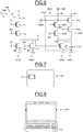
- the figure 1 illustrates an inverting type logic circuit CL coupled between a first terminal B1, intended to receive a supply voltage Vdd, and a second terminal B2, intended to receive a reference voltage, for example here the ground GND.
- the logic circuit conventionally comprises an input terminal E and an output terminal S.
- the output terminal S can here be coupled to the input of another component of the integrated circuit IC (not shown), for example to another inverter. This coupling can generate parasitic capacitances, due for example to the gate capacitances of the transistors of the other inverter.
- this parasitic capacitance is represented by a first capacitor C1.
- the logic circuit CL conventionally comprises an NMOS transistor TN1 coupled in series with a PMOS transistor TP1 between the first terminal B1 and the second terminal B2.
- the input terminal E of the logic circuit is coupled to the gates of the two transistors, and the output terminal S is coupled to the node common to the two transistors, here the node common to the drain of the PMOS transistor TP1 and the drain of the NMOS transistor TN1.
- the PMOS transistor TP1 becomes on and the NMOS transistor TN1 becomes off.
- the capacitor C1 is then charged by the current I C1 flowing through the PMOS transistor TP1.
- the charging time of the capacitor being very short, this current can be likened to a peak load current Ic 1 .
- the peak current generated during a transition of the signal delivered by the output terminal S from a low state to a high state may have a value different from that of the current peak generated during a transition of a high state. to a low state.
- the logic circuit CL consumes a current greater than that which it consumes during a transition from a low state to a high state, since in the first case the consumed current is the sum of the load current Ic 1 of the capacitor C1 and the short-circuit current and in the second case the consumed current corresponds only to the short-circuit current Ic 2 .
- this solution is restrictive since it also means masking the current consumption of logic gates whose consumption does not have to be masked. Otherwise, this technique is expensive on the surface, since it requires doubling the number of logic gates of the integrated circuit.
- an electronic device comprising at least one logic circuit which comprises a first terminal intended to receive a supply voltage, a second terminal intended to receive a reference voltage, and at least one output terminal, the output terminal being configured to output a signal that may be in a high state or a low state.
- This device comprises at least one auxiliary circuit coupled between the first terminal and the second terminal and configured to randomly generate an additional current between the first terminal and the second terminal at each change of state of the signal on the output terminal. .
- the current consumption of the logic circuit is masked by the random generation of an additional current that is similar to noise, and it is more difficult to deduce the operations performed by the logic circuit by an analysis of its current consumption.
- the integrated circuit which incorporates this logic circuit can thus for example be protected against analyzes by auxiliary channel ("Side Channel Analysis" according to the Anglo-Saxon name well known to those skilled in the art).
- auxiliary module to the logic circuit eliminates the need for a global masking of the power consumption of the integrated circuit.
- this logic circuit comprises at least one input terminal
- the auxiliary circuit comprises an auxiliary input terminal configured to receive a pseudo-random signal and comprises a first auxiliary transistor whose control electrode is coupled to the auxiliary input terminal and of which a first electrode is coupled to the first terminal, at least one second auxiliary transistor whose control electrode is coupled to the output of the logic circuit, and at least one intermediate transistor coupled between the first auxiliary transistor and said at least one second auxiliary transistor and whose control electrode is coupled to said at least one input.
- said at least one logic circuit may be an inverter.
- the auxiliary circuit comprises several intermediate transistors, each intermediate transistor having its gate coupled to a separate input of the logic circuit.
- the device is compatible with different types of logic circuit.
- the intermediate transistors may be connected in series between the first auxiliary transistor and the second auxiliary transistor.
- Said at least one logic circuit may comprise a NAND logic gate, and the auxiliary circuit then comprises a first intermediate transistor whose control electrode is coupled to a first input terminal of the NAND gate and a second transistor. intermediate whose control electrode is coupled to a second input terminal of the NAND gate, the first auxiliary transistor, the second auxiliary transistor, the first intermediate transistor and the second intermediate transistor being connected in series between the first terminal and the second terminal.
- the auxiliary circuit may comprise a third auxiliary transistor whose control electrode is coupled to the auxiliary input terminal, and the intermediate transistors have a first mutually coupled electrode and are respectively coupled in series with the first and third auxiliary transistors.
- said at least one logic circuit comprises a NOR gate
- the device comprises the first intermediate transistor connected in series with the first auxiliary transistor and whose control electrode is coupled to a first input of the NOR gate, a second intermediate transistor whose control electrode is coupled to a second input of the NOR gate and connected in series with the third auxiliary transistor whose control electrode is coupled to the pseudo signal generator; random, the first auxiliary transistor and the first intermediate transistor being connected in parallel with the third auxiliary transistor and the second intermediate transistor between the supply terminal and the first intermediate transistor.
- the device may include a plurality of connected modules.
- an integrated circuit comprising a device as described above.
- a system comprising at least one integrated circuit, the system may for example form a smart card or a computer device.
- the first auxiliary transistor and the third auxiliary transistor may be PMOS transistors, and the second transistor and the intermediate transistors may be NMOS transistors.
- a system comprising an integrated circuit, the system may be a smart card or a computer system.
- the figure 2 illustrates schematically from an electrical point of view an integrated circuit CI comprising an electronic device incorporating an MS module containing a logic circuit CL having an input terminal E and an output terminal S and coupled to an auxiliary module MDX.
- the logic circuit CL and the auxiliary module MDX are both coupled between a first terminal B1 intended to receive a supply voltage Vdd, and a second terminal B2 intended to receive a reference voltage, for example here the ground GND.
- the logic circuit CL is here an invertor INV which conventionally comprises a first PMOS transistor TP1 and a first NMOS transistor TN2 connected in series between the first terminal B1 and the second terminal B2.
- the inverter INV comprises the input terminal E, coupled to the gate of the first PMOS transistor TP1 and to the gate of the first NMOS transistor TN1, and the output terminal S coupled between the first NMOS transistor TN1 and the first PMOS transistor TP1. .
- the output terminal S can here be coupled to the input of another component of the integrated circuit IC (not shown), for example to another inverter.
- This coupling can generate parasitic capacitances, due in particular to the gate capacitance of the other inverter.
- this parasitic capacitance is represented by a first capacitor C1.
- the auxiliary module MDX comprises an auxiliary circuit AUX having an auxiliary input EAX, and a pseudo-random signal generator RDM coupled to the auxiliary input EAX of the auxiliary circuit AUX.
- the pseudo-random signal generator RDM of conventional structure and known per se, is configured to generate a signal can be randomly in a high state or in a low state.
- This RDM generator may be specific to the MS module, or be common to other modules of the integrated circuit.
- Auxiliary circuit AUX here comprises a first auxiliary transistor TP2, here a PMOS transistor, and a second auxiliary transistor TN2, here an NMOS transistor, coupled in series between the first terminal B1 and the second terminal B2.
- the gate of the first intermediate transistor TN3 is coupled to the input terminal E of the inverter INV, and the gate of the second auxiliary transistor TN2 is coupled to the output terminal S of the inverter INV.
- the gate of the first auxiliary transistor TP2 forms the auxiliary input EAX and is therefore coupled to the pseudo-random signal generator RDM.
- the auxiliary circuit AUX is here coupled to another module of the integrated circuit CI, for example to an inverter (not shown), and this coupling can generate a parasitic capacitance represented on the figure 2 by a second capacitor C2.
- the input terminal E of the integrated circuit receives a signal in the high state, for example a voltage of value 3 volts, the first PMOS transistor TP1 is thus blocked, and the first NMOS transistor TN1 is on.
- the output terminal S then delivers a signal in the low state, for example a zero voltage.
- the second auxiliary transistor TN2 is therefore in a blocked state.
- the first intermediate transistor TN3 is coupled to the input terminal E, it is in an on state.
- the first capacitor C1 is then charged thanks to the circulation of a first peak of charge current flowing between the first terminal B1 and ground GND, through the first PMOS transistor TP1 and the first capacitor C1.
- the simultaneous switching of the first NMOS transistor TN1 and the first PMOS transistor TP1 causes the circulation of a first short-circuit current peak between the first terminal B1 and the second terminal B2, through the first PMOS transistor TP1 and the first NMOS transistor TN1.
- the first capacitor C1 then discharges through the first NMOS transistor TN1.
- the simultaneous switching of the first NMOS transistor TN1 and the first PMOS transistor TP1 causes the circulation of a second short-circuit current peak, between the first terminal B1 and the second terminal B2, through the first PMOS transistor.
- the logic circuit CL consumes a current equal to the sum of the first peak of load current and the first peak of short circuit current, and during the second transition, the logic circuit CL consumes a current lower, equal to the second peak of short-circuit current.
- the first intermediate transistor TN3 being coupled to the input terminal E, it goes into an on state.
- the second auxiliary transistor TN2 whose gate is coupled to the output terminal S, goes into a blocked state.
- the simultaneous switching of the first auxiliary transistor TP2, the second auxiliary transistor TN2 and the first intermediate transistor TN3 causes the circulation of a third current peak between the first terminal B1 and the second terminal B2, through these three transistors.
- the signal delivered by the pseudo-random signal generator keeps a high state, then the first auxiliary transistor TP2 was in a blocked state and remains in a blocked state, and no current peak flows in the auxiliary circuit AUX.
- the first auxiliary transistor TP2 retains its on state, and the simultaneous switching of the second auxiliary transistor TN2 and the first intermediate transistor TN3 generates a fourth current peak. short circuit between the first terminal B1 and the second terminal B2.
- the current consumption of the logic circuit CL is thus masked, and it is more difficult for an external attacker to determine the nature of the operations performed by the module MS of the IC circuit by studying the current consumption.
- figure 3 illustrates a lock LT1 ("Latch" in English) comprising two modules MS1 and MS2 having a structure similar to that described above in connection with the figure 2 .
- the first module MS1 and the second module MS2 each respectively have an input E1 and E2 and an auxiliary input EAX1 and EAX2.
- each module MS1, MS2 is represented by a conventional inverter symbol comprising an auxiliary input EAX1 and EAX2 coupled to the pseudo-random signal generator RDM common to the two inverters.
- the figure 5 illustrates an embodiment wherein the logic circuit CL is a NAND gate 4, having a first input terminal E1 and a second input terminal E2.
- the NAND gate 4 conventionally comprises two PMOS transistors T1 and T2 coupled in parallel, the pair of transistors T1 and T2 being connected in series with two NMOS transistors T3 and T4 between the first terminal B1 and the second terminal B2.
- Each of the input terminals E1 and E2 is coupled to the gate of a separate PMOS transistor T1 or T2 and to the gate of a separate NMOS transistor T3 or T4.
- AUX auxiliary circuit is modified with respect to the previous embodiment so as to include a second intermediate transistor TN4 coupled between the first intermediate transistor TN3 and the second auxiliary transistor TN2.
- the gate of the first intermediate transistor TN3 is coupled to the first input terminal E1, and the gate of the second intermediate transistor TN4 is coupled to the second input terminal E2.
- the first intermediate transistor TN3, the second intermediate transistor TN4 and the second auxiliary transistor TN2 change state.
- the first auxiliary transistor TP2 via the pseudo-random signal generator RDM, changes state, or if it retains an on state, a peak current flows between the first terminal B1 and the second terminal B2.
- the intensity of this current peak depends on the nature of the switching of the transistors of the auxiliary circuit AUX.
- the figure 6 illustrates an embodiment of the invention wherein the logic circuit CL is a NOR gate having the first input terminal E1 and a second input terminal E2.
- the NOR gate 5 differs conventionally from the NAND gate 4 of the figure 5 in that the two PMOS transistors T1 and T2 are coupled in series and the two NMOS transistors T3 and T4 are coupled in parallel, the two transistor pairs T1-T2 and T3-T4 being coupled in series with each other .
- the auxiliary circuit AUX is modified with respect to the embodiment described above in connection with the figure 4 so that a third auxiliary transistor TP3, here a PMOS transistor, and the second intermediate transistor TN4 are connected in series between the first terminal B1 and the second NMOS transistor TN2, and so as to be connected in parallel with the first auxiliary transistor TP2 and the first intermediate transistor TN3.
- a third auxiliary transistor TP3, here a PMOS transistor, and the second intermediate transistor TN4 are connected in series between the first terminal B1 and the second NMOS transistor TN2, and so as to be connected in parallel with the first auxiliary transistor TP2 and the first intermediate transistor TN3.
- the gate of the first auxiliary transistor TP2 and the gate of the third auxiliary transistor TP3 are coupled to the pseudo-random signal generator RDM.
- the gate of the first intermediate transistor TN3 is coupled to the first input terminal E1 and the gate of the second intermediate transistor TN4 is coupled to the second input terminal E2.
- the first intermediate transistor TN3 and / or the second intermediate transistor TN4 change state.
- first auxiliary transistor TP2 and the third auxiliary transistor TP3 via the pseudo-random signal generator RDM, change state, or if they maintain an on state, a peak current flows between the first terminal B1 and the second terminal B2.
- the integrated electronic circuit CI previously described and illustrated in Figures 2 to 6 can conventionally be integrated in a system comprising a processing unit, typically in a processing unit of a smart card, a computer, or a mobile terminal, which require the implementation of secure operations .
- the Figures 7 and 8 illustrate computer systems comprising secure processing units in which integrated circuits IC are incorporated according to one embodiment of the invention.
- the figure 7 illustrates a CP smart card and the figure 8 illustrates a CMP laptop.
- the smart card CP and the laptop CMP comprise for example a microprocessor comprising an integrated circuit according to one embodiment of the invention.
Landscapes
- Engineering & Computer Science (AREA)
- Computer Hardware Design (AREA)
- Physics & Mathematics (AREA)
- Theoretical Computer Science (AREA)
- General Engineering & Computer Science (AREA)
- Computer Security & Cryptography (AREA)
- General Physics & Mathematics (AREA)
- Software Systems (AREA)
- Mathematical Physics (AREA)
- Microelectronics & Electronic Packaging (AREA)
- Computing Systems (AREA)
- Logic Circuits (AREA)
- Semiconductor Integrated Circuits (AREA)
- Metal-Oxide And Bipolar Metal-Oxide Semiconductor Integrated Circuits (AREA)
Abstract
Description
- Des modes de mise en oeuvre et de réalisation de l'invention concernent les circuits intégrés, et notamment mais non exclusivement ceux comportant des circuits logiques, et en particulier la gestion de la consommation en courant de ce type de circuit en fonctionnement, par exemple en vu de masquer cette consommation de courant.
- La
figure 1 illustre un circuit logique CL de type inverseur couplé entre une première borne B1, destinée à recevoir une tension d'alimentation Vdd, et une deuxième borne B2, destinée à recevoir une tension de référence, par exemple ici la masse GND. Le circuit logique comprend classiquement une borne d'entrée E et une borne de sortie S. - La borne de sortie S peut être ici couplée à l'entrée d'un autre composant du circuit intégré CI (non-représenté), par exemple à un autre inverseur. Ce couplage peut générer des capacités parasites, dues par exemple aux capacités de grille des transistors de l'autre inverseur.
- Sur la
figure 1 , cette capacité parasite est représentée par un premier condensateur C1. - Le circuit logique CL comporte classiquement un transistor NMOS TN1 couplé en série avec un transistor PMOS TP1 entre la première borne B1 et la deuxième borne B2. La borne d'entrée E du circuit logique est couplée aux grilles des deux transistors, et la borne de sortie S est couplée au noeud commun aux deux transistors, ici le noeud commun au drain du transistor PMOS TP1 et au drain du transistor NMOS TN1.
- Ainsi, lors de la transition du signal présent sur la borne d'entrée E d'un état haut vers un état bas, le transistor PMOS TP1 devient passant et le transistor NMOS TN1 devient bloqué. Le condensateur C1 se charge alors grâce au courant IC1 circulant au travers du transistor PMOS TP1. Le temps de charge du condensateur étant très court, ce courant peut être assimilé à un pic de courant de charge Ic1.
- De plus, la commutation simultanée des deux transistors crée pendant un court intervalle de temps un court-circuit entre les bornes B1 et B2. Cet intervalle de temps est d'autant plus important que la commutation est lente. Ainsi, à chaque commutation, un pic de courant de court circuit Ic2 circule entre la première borne B1 et la deuxième borne B2 au travers des deux transistors TP1 et TN1.
- Le pic de courant généré lors d'une transition du signal délivré par la borne de sortie S d'un état bas vers un état haut peut avoir une valeur différente de celle du pic de courant généré lors d'une transition d'un état haut vers un état bas.
- Lors d'une transition du signal présent sur la borne d'entrée E d'un état haut vers un état bas, le circuit logique CL consomme un courant supérieur à celui qu'il consomme lors d'une transition d'un état bas vers un état haut, puisque dans le premier cas le courant consommé est la somme du courant de charge Ic1 du condensateur C1 et du courant de court-circuit et dans le deuxième cas le courant consommé correspond seulement au courant de court-circuit Ic2.
- Ainsi, en analysant la consommation en courant d'un circuit intégré comportant une des portes logiques, à l'aide par exemple d'une sonde électromagnétique et d'algorithmes dédiés, il est possible d'obtenir des informations sur les opérations effectuées ainsi que sur les données manipulées et/ou sur leurs occurrences.
- Il est donc recommandé de masquer autant que possible la consommation en courant du circuit intégré.
- Il existe des solutions pour masquer la consommation en courant d'un circuit intégré, comme par exemple la technique du double rail (« Dual rail technique » en langue anglaise ) qui lisse la consommation en courant d'un circuit intégré en générant un courant complémentaire au courant de consommation réel des circuits logiques du circuit.
- Cela étant cette solution est contraignante puisqu'elle implique de masquer également la consommation en courant de portes logiques dont il n'est pas nécessaire de masquer la consommation. Par ailleurs, cette technique est coûteuse en surface, puisqu'elle nécessite de doubler le nombre de portes logiques du circuit intégré.
- Ainsi, selon un mode de réalisation, il est proposé de masquer la consommation en courant d'un circuit logique incorporé au sein d'un circuit intégré, en utilisant des moyens simples permettant de focaliser le masquage sur le circuit logique.
- Selon un aspect, il est proposé un procédé de gestion de la consommation en courant d'un circuit logique alimenté entre une première borne et une deuxième borne et comportant au moins une borne de sortie, dans lequel on génère ou non aléatoirement un courant supplémentaire entre la première borne et la deuxième borne lorsque le signal délivré par ladite au moins une borne de sortie du circuit logique change d'état.
- Selon un autre aspect, il est proposé un dispositif électronique comprenant au moins un circuit logique qui comporte une première borne destinée à recevoir une tension d'alimentation, une deuxième borne destinée à recevoir une tension de référence, et au moins une borne de sortie, la borne de sortie étant configurée pour délivrer un signal pouvant être dans un état haut ou dans un état bas.
- Ce dispositif comprend au moins un circuit auxiliaire couplé entre la première borne et la deuxième borne et configuré pour générer ou non de façon aléatoire un courant supplémentaire entre la première borne et la deuxième borne à chaque changement d'état du signal sur la borne de sortie.
- Ainsi, la consommation en courant du circuit logique est masquée par la génération aléatoire d'un courant supplémentaire qui s'apparente à du bruit, et il est plus difficile de déduire les opérations effectuées par le circuit logique par une analyse de sa consommation en courant. Le circuit intégré qui incorpore ce circuit logique peut ainsi par exemple être protégé contre les analyses par canaux auxiliaire (« Side Channel Analysis » selon la dénomination anglo-saxonne bien connue de l'homme du métier).
- De plus, en couplant le module auxiliaire au circuit logique, on s'affranchit de la réalisation d'un masquage global de la consommation en courant du circuit intégré. En particulier, il est possible de réaliser un circuit intégré comportant une pluralité de circuits logiques dans lequel seuls certains circuits logiques sont couplés à un module auxiliaire, et ont donc une consommation en courant masquée.
- Selon une variante de réalisation, ce circuit logique comporte au moins une borne d'entrée, et le circuit auxiliaire comporte une borne d'entrée auxiliaire configurée pour recevoir un signal pseudo-aléatoire et comprend un premier transistor auxiliaire dont l'électrode de commande est couplée à la borne d'entrée auxiliaire et dont une première électrode est couplée à la première borne, au moins un deuxième transistor auxiliaire dont l'électrode de commande est couplée à la sortie du circuit logique, et au moins un transistor intermédiaire couplé entre le premier transistor auxiliaire et ledit au moins un deuxième transistor auxiliaire et dont l'électrode de commande est couplée à ladite au moins une entrée.
- Par exemple, ledit au moins un circuit logique peut être un inverseur.
- Selon une autre variante de réalisation applicable à un circuit logique comportant plusieurs entrées, le circuit auxiliaire comporte plusieurs transistors intermédiaires, chaque transistor intermédiaire ayant sa grille couplée à une entrée distincte du circuit logique.
- Ainsi, le dispositif est compatible avec différents type de circuit logique.
- Les transistors intermédiaires peuvent être connectés en série entre le premier transistor auxiliaire et le deuxième transistor auxiliaire.
- Ledit au moins un circuit logique peut comporter une porte logique NON-ET, et le circuit auxiliaire comporte alors un premier transistor intermédiaire dont l'électrode de commande est couplée à une première borne d'entrée de la porte NON-ET et un deuxième transistor intermédiaire dont l'électrode de commande est couplée à une deuxième borne d'entrée de la porte NON-ET, le premier transistor auxiliaire, le deuxième transistor auxiliaire, le premier transistor intermédiaire et le deuxième transistor intermédiaire étant montés en série entre la première borne et deuxième borne.
- Le circuit auxiliaire peut comprendre un troisième transistor auxiliaire dont l'électrode de commande est couplée à la borne d'entrée auxiliaire, et les transistors intermédiaires ont une première électrode mutuellement couplée et sont respectivement couplés en série avec les premier et troisième transistors auxiliaires.
- Selon un autre mode de réalisation, ledit au moins un circuit logique comporte une porte NON-OU, et le dispositif comporte le premier transistor intermédiaire connectés en série avec le premier transistor auxiliaire et dont l'électrode de commande est couplée à une première entrée de la porte NON-OU, un deuxième transistor intermédiaire dont l'électrode de commande est couplée à une deuxième entrée de la porte NON-OU et monté en série avec le troisième transistor auxiliaire dont l'électrode de commande est couplée au générateur de signal pseudo-aléatoire, le premier transistor auxiliaire et le premier transistor intermédiaire étant connectés en parallèle avec le troisième transistor auxiliaire et le deuxième transistor intermédiaire entre la borne d'alimentation et le premier transistor intermédiaire.
- Le dispositif peut comprendre plusieurs modules connectés.
- Selon un autre aspect, il est proposé un circuit intégré comprenant un dispositif tel que décrit précédemment.
- Selon un autre aspect, il est proposé un système comprenant au moins un circuit intégré, le système pouvant par exemple former une carte à puce ou un appareil informatique.
- Le premier transistor auxiliaire et le troisième transistor auxiliaire peuvent être des transistors PMOS, et le deuxième transistor et les transistors intermédiaires peuvent être des transistors NMOS.
- Selon un autre aspect, il est proposé un système comprenant un circuit intégré, le système pouvant être une carte à puce ou un système informatique.
- D'autres avantages et caractéristiques de l'invention apparaitront à l'examen de la description détaillée de modes de mise en oeuvre et de réalisation de l'invention, nullement limitatifs, et des dessins annexés sur lesquels :
- la
figure 1 , décrite précédemment, illustre un circuit logique inverseur classique, - les
figures 2 à 8 illustrent des modes de mise en oeuvre et de réalisation de l'invention. - La
figure 2 illustre schématiquement d'un point de vue électrique un circuit intégré CI comportant un dispositif électronique incorporant un module MS contenant un circuit logique CL comportant une borne d'entrée E et une borne de sortie S et couplée à un module auxiliaire MDX. - Le circuit logique CL et le module auxiliaire MDX sont tous les deux couplés entre une première borne B1 destinée à recevoir une tension d'alimentation Vdd, et une deuxième borne B2 destinée à recevoir une tension de référence, par exemple ici la masse GND.
- Le circuit logique CL est ici un inverseur INV qui comporte classiquement un premier transistor PMOS TP1 et un premier transistor NMOS TN2 montés en série entre la première borne B1 et la deuxième borne B2.
- L'inverseur INV comporte la borne d'entrée E, couplée à la grille du premier transistor PMOS TP1 et à la grille du premier transistor NMOS TN1, et la borne de sortie S couplée entre le premier transistor NMOS TN1 et le premier transistor PMOS TP1.
- La borne de sortie S peut être ici couplée à l'entrée d'un autre composant du circuit intégré CI (non-représenté), par exemple à un autre inverseur. Ce couplage peut générer des capacités parasites, dues notamment à la capacité de grille de l'autre inverseur. Sur la
figure 1 , cette capacité parasite est représentée par un premier condensateur C1. - Le module auxiliaire MDX comporte un circuit auxiliaire AUX comportant une entrée auxiliaire EAX, et un générateur de signal pseudo-aléatoire RDM couplé à l'entrée auxiliaire EAX du circuit auxiliaire AUX.
- Le générateur de signal pseudo-aléatoire RDM, de structure classique et connue en soi, est configuré pour générer un signal pouvant être aléatoirement dans un état haut ou dans un état bas. Ce générateur RDM peut être spécifique au module MS, ou être commun à d'autres modules du circuit intégré.
- Le circuit auxiliaire AUX comporte ici un premier transistor auxiliaire TP2, ici un transistor PMOS, et un deuxième transistor auxiliaire TN2, ici un transistor NMOS, couplés en série entre la première borne B1 et la deuxième borne B2.
- Un premier transistor intermédiaire TN3, ici un transistor NMOS, est couplé entre le premier transistor auxiliaire TP2 et le deuxième transistor auxiliaire TN2.
- La grille du premier transistor intermédiaire TN3 est couplée à la borne d'entrée E de l'inverseur INV, et la grille du deuxième transistor auxiliaire TN2 est couplée à la borne de sortie S de l'inverseur INV.
- La grille du premier transistor auxiliaire TP2 forme l'entrée auxiliaire EAX et est donc couplée au générateur de signal pseudo-aléatoire RDM.
- Le circuit auxiliaire AUX est ici couplé à un autre module du circuit intégré CI, par exemple à un inverseur (non représenté), et ce couplage peut générer une capacité parasite représentée sur la
figure 2 par un deuxième condensateur C2. - Initialement, la borne d'entrée E du circuit intégré reçoit un signal à l'état haut, par exemple une tension de valeur 3 volts, le premier transistor PMOS TP1 est donc bloqué, et le premier transistor NMOS TN1 est passant.
- La borne de sortie S délivre alors un signal à l'état bas, par exemple une tension nulle. Le deuxième transistor auxiliaire TN2 est donc dans un état bloqué.
- Et, puisque le premier transistor intermédiaire TN3 est couplé à la borne d'entrée E, il est dans un état passant.
- Lors d'une première transition, c'est-à-dire lorsque le signal sur l'entrée E passe dans un état bas, alors le premier transistor PMOS TP1 passe dans un état passant et le premier transistor NMOS TN1 passe dans un état bloqué. Le signal délivré par la borne de sortie S passe donc d'un état bas à un état haut.
- Le premier condensateur C1 se charge alors grâce à la circulation d'un premier pic de courant de charge circulant entre la première borne B1 et la masse GND, au travers du premier transistor PMOS TP1 et du premier condensateur C1.
- Et, la commutation simultanée du premier transistor NMOS TN1 et du premier transistor PMOS TP1 entraine la circulation d'un premier pic de courant de court-circuit entre la première borne B1 et la deuxième borne B2, au travers du premier transistor PMOS TP1 et du premier transistor NMOS TN1.
- Et lors d'une deuxième transition, c'est à dire lorsque le signal sur la borne d'entrée E passe de nouveau dans un état haut, alors le premier transistor PMOS TP1 passe dans un état bloqué et le premier transistor NMOS TN1 passe dans un état passant. Le signal délivré par la borne de sortie S passe alors d'un état haut à un état bas.
- Le premier condensateur C1 se décharge alors au travers du premier transistor NMOS TN1.
- Et de nouveau, la commutation simultanée du premier transistor NMOS TN1 et du premier transistor PMOS TP1 entraine la circulation d'un deuxième pic de courant de court-circuit, entre la première borne B1 et la deuxième borne B2, au travers du premier transistor PMOS TP1 et du premier transistor NMOS TN1.
- Ainsi, lors de la première transition, le circuit logique CL consomme un courant égal à la somme du premier pic de courant de charge et du premier pic de courant de court circuit, et lors de la deuxième transition, le circuit logique CL consomme un courant plus faible, égal au deuxième pic de courant de court-circuit.
- Lors d'une analyse par canaux auxiliaires, cette différence de consommation permet l'analyse du comportement du circuit en l'absence du circuit auxiliaire AUX.
- La présence de ce circuit auxiliaire va permettre de masquer la consommation du circuit logique CL comme cela va maintenant être expliqué.
- Lors de la deuxième transition, le premier transistor intermédiaire TN3 étant couplé à la borne d'entrée E, il passe dans un état passant.
- Le deuxième transistor auxiliaire TN2, dont la grille est couplée à la borne de sortie S, passe dans un état bloqué.
- La grille du premier transistor auxiliaire TP2 étant couplée au générateur de signal pseudo-aléatoire RDM, le premier transistor auxiliaire TP2 peut soit changer d'état si le signal généré par le générateur RDM change d'état, par exemple en passant d'un état haut à un état bas ou d'un état bas à un état haut, soit conserver sont état si le signal généré par le générateur RDM ne change pas d'état.
- Et, si le premier transistor auxiliaire TP2 change d'état, alors la commutation simultanée du premier transistor auxiliaire TP2, du deuxième transistor auxiliaire TN2 et du premier transistor intermédiaire TN3 entraîne la circulation d'un troisième pic de courant entre la première borne B1 et la deuxième borne B2, au travers de ces trois transistors.
- Si ce changement d'état correspond à un passage de l'état bloqué à l'état passant, alors un deuxième pic de courant de charge circule entre la première borne B1 et la masse de façon à charger le deuxième condensateur C2.
- Si le signal délivré par le générateur de signal pseudo aléatoire conserve un état haut, alors le premier transistor auxiliaire TP2 était dans un état bloqué et reste dans un état bloqué, et aucun pic de courant ne circule dans le circuit auxiliaire AUX.
- Si le signal délivré par le générateur de signal pseudo-aléatoire RDM conserve un état bas, alors le premier transistor auxiliaire TP2 conserve son état passant, et la commutation simultanée du deuxième transistor auxiliaire TN2 et du premier transistor intermédiaire TN3 génère un quatrième pic de courant de court circuit entre la première borne B1 et la deuxième borne B2.
- Ainsi, lors de la deuxième transition, c'est-à-dire lorsque le signal délivré par la borne de sortie S passe d'un état haut vers un état bas, on génère aléatoirement
- un pic de courant égal à la somme du deuxième pic de courant de charge et du troisième pic de courant de court-circuit,
- le quatrième pic de courant, ou
- aucun pic de courant.
- La consommation en courant du circuit logique CL est donc masquée, et il est plus difficile pour un attaquant extérieur de déterminer la nature des opérations effectuées par le module MS du circuit CI par l'étude de la consommation en courant.
- Lors de la première transition, c'est-à-dire lorsque le signal délivré sur la borne de sortie S passe d'un état bas vers un état haut, seuls des pics de courant de court-circuit sont générés par le circuit auxiliaire AUX.
- Le mode de réalisation de l'invention décrit précédemment est compatible avec des circuits logiques séquentiels. En particulier, la
figure 3 illustre un verrou LT1 (« Latch » en langue anglaise) comportant deux modules MS1 et MS2 ayant une structure analogue à celle décrite précédemment en lien avec lafigure 2 . - Le premier module MS1 et le deuxième module MS2 comportent chacun respectivement une entrée E1 et E2 et une entrée auxiliaire EAX1 et EAX2.
- Sur la
figure 3 , chaque module MS1, MS2 est représenté par un symbole d'inverseur classique comprenant une entrée auxiliaire EAX1 et EAX2 couplée au générateur de signal pseudo-aléatoire RDM commun aux deux inverseurs. - Comme illustré sur la
figure 4 , il serait également possible de coupler une pluralité de verrou LT1, LT2 en série de façon à former un registre à décalage RD et en conservant un seul générateur de signal pseudo aléatoire commun connecté aux entrée EAX11, EAX12, EAX21 et EAX22, ou en utilisant un générateur de signal pseudo-aléatoire différents pour chaque entrée. - Il serait également envisageable d'utiliser un générateur pseudo-aléatoire à plusieurs bits parallèle respectivement affectés aux différents verrous de façon à augmenter d'avantage la complexité du bruit.
- La
figure 5 illustre un mode de réalisation dans lequel le circuit logique CL est une porte NON-ET 4, comportant une première borne d'entrée E1 et une deuxième borne d'entrée E2. - La porte NON-ET 4 comporte classiquement deux transistors PMOS T1 et T2 couplés en parallèle, le couple de transistors T1 et T2 étant montés en série avec deux transistors NMOS T3 et T4 entre la première borne B1 et la deuxième borne B2.
- Chacune des bornes d'entrée E1 et E2 est couplée à la grille d'un transistor PMOS T1 ou T2 distinct et à la grille d'un transistor NMOS T3 ou T4 distinct.
- Le circuit auxiliaire AUX est modifié par rapport au mode de réalisation précédent de manière à comprendre un deuxième transistor intermédiaire TN4 couplé entre le premier transistor intermédiaire TN3 et le deuxième transistor auxiliaire TN2.
- La grille du premier transistor intermédiaire TN3 est couplée à la première borne d'entrée E1, et la grille du deuxième transistor intermédiaire TN4 est couplée à la deuxième borne d'entrée E2.
- Ainsi, lors d'une transition du signal présent sur la borne de sortie S, c'est-à-dire lorsque le couple de signaux sur le couple de bornes d'entrée E1-E2, passe d'un état bas-bas, bas-haut, ou haut-bas vers un état haut-haut, ou inversement, alors le premier transistor intermédiaire TN3, le deuxième transistor intermédiaire TN4 et le deuxième transistor auxiliaire TN2 changent d'état.
- Et, si le premier transistor auxiliaire TP2, via le générateur de signal pseudo-aléatoire RDM, change d'état, ou s'il conserve un état passant, un pic de courant circule entre la première borne B1 et la deuxième borne B2. L'intensité de ce pic de courant dépend de la nature des commutations des transistors du circuit auxiliaire AUX.
- Et plus particulièrement, lorsque le couple de signaux sur le couple de bornes d'entrée E1-E2, passe d'un état bas-bas, bas-haut, ou haut-bas vers un état haut-haut, et si le premier transistor auxiliaire TP2, via le générateur de signal pseudo-aléatoire RDM, passe d'un état bas à un état haut, alors un pic de courant de charge circule entre la première borne B1 et la masse de façon à charger le deuxième condensateur C2.
- Ainsi lors de certaines transitions seulement, et donc de façon aléatoire, on génère un signal de bruit rendant plus difficile la détermination des opérations effectuées.
- La
figure 6 illustre un mode de réalisation de l'invention dans lequel le circuit logique CL est une porte NON-OU 5 comportant la première borne d'entrée E1 et une deuxième borne d'entrée E2. - La porte NON-OU 5 diffère classiquement de la porte NON-ET 4 de la
figure 5 en ce que les deux transistors PMOS T1 et T2 sont couplés en série et les deux transistors NMOS T3 et T4 sont couplés en parallèle, les deux couples de transistor T1-T2 et T3-T4 étant couplés en série l'un avec l'autre. - Dans ce mode de réalisation, le circuit auxiliaire AUX est modifié par rapport au mode de réalisation décrit précédemment en lien avec la
figure 4 de manière à ce qu'un troisième transistor auxiliaire TP3, ici un transistor PMOS, et le deuxième transistor intermédiaire TN4 soient montés en série entre la première borne B1 et le deuxième transistor NMOS TN2, et de façon à être montés en parallèle avec le premier transistor auxiliaire TP2 et le premier transistor intermédiaire TN3. - La grille du premier transistor auxiliaire TP2 et la grille du troisième transistor auxiliaire TP3 sont couplées au générateur de signal pseudo-aléatoire RDM.
- La grille du premier transistor intermédiaire TN3 est couplée à la première borne d'entrée E1 et la grille du deuxième transistor intermédiaire TN4 est couplée à la deuxième borne d'entrée E2.
- Ainsi, lors d'une transition du signal sur la borne de sortie S de la porte NON-OU 5, c'est-à-dire une transition du couple de signaux sur le couple d'entrées E1-E2 d'un état bas-bas vers un état bas-haut, haut-bas ou haut-haut, ou inversement, alors le premier transistor intermédiaire TN3 et/ou le deuxième transistor intermédiaire TN4 changent d'état.
- Et, si le premier transistor auxiliaire TP2 et le troisième transistor auxiliaire TP3, via le générateur de signal pseudo-aléatoire RDM, changent d'état, ou s'ils conservent un état passant, un pic de courant circule entre la première borne B1 et la deuxième borne B2.
- Et, plus particulièrement, lors d'une transition du couple de signaux sur le couple d'entrées E1-E2 d'un état bas-bas vers un état bas-haut, haut-bas ou haut-haut et si le premier transistor auxiliaire TP2 et le troisième transistor auxiliaire TP3 passe d'un état bloqué à un état passant, alors un pic de courant de charge circule entre la borne B1 et la masse GND, de façon à charger le deuxième condensateur C2.
- Le circuit électronique intégré CI décrit précédemment et illustré aux
figures 2 à 6 peut classiquement être intégré à un système comprenant une unité de traitement, classiquement dans une unité de traitement d'une carte à puce, d'un ordinateur, ou d'un terminal de téléphonie mobile, qui nécessitent la mise en oeuvre d'opérations sécurisées. - Les
figures 7 et 8 illustrent des systèmes informatiques comportant des unités de traitement sécurisées dans lesquelles sont incorporés des circuits intégrés CI selon un mode de réalisation de l'invention. Lafigure 7 illustre une carte à puce CP et lafigure 8 illustre un ordinateur portable CMP. La carte à puce CP et l'ordinateur portable CMP comportent par exemple un microprocesseur comportant un circuit intégré selon un mode de réalisation de l'invention.
Claims (14)
- Procédé de gestion de la consommation en courant d'un circuit logique (CL) alimenté entre une première borne et une deuxième borne et comportant au moins une borne de sortie (S), dans lequel on génère ou non aléatoirement un courant supplémentaire entre la première borne et la deuxième borne lorsque le signal délivré par ladite au moins une borne de sortie (S) du circuit logique (CL) change d'état.
- Dispositif électronique comprenant au moins un module (MS) contenant au moins un circuit logique (CL) qui comporte une première borne (B1) destinée à recevoir une tension d'alimentation (Vdd), une deuxième borne (B2) destinée à recevoir une tension de référence (GND), et au moins une borne de sortie (S), la borne de sortie (S) étant configurée pour délivrer un signal pouvant être dans un état haut ou un état bas, au moins un circuit auxiliaire (AUX) couplé entre la première borne (B1) et la deuxième borne (B2) et configuré pour générer ou non de façon aléatoire un courant supplémentaire entre la première borne (B1) et la deuxième borne (B2) à chaque changement d'état du signal sur la borne de sortie (S).
- Dispositif selon la revendication 2, dans lequel le circuit logique (CL) comporte au moins une borne d'entrée (E), et dans lequel le circuit auxiliaire (AUX) comporte une borne d'entrée auxiliaire (EAX) configurée pour recevoir un signal pseudo-aléatoire (RDM) et comprend un premier transistor auxiliaire (TP2) dont l'électrode de commande est couplée à la borne d'entrée auxiliaire (EAX) et dont une première électrode est couplée à la première borne (B1), au moins un deuxième transistor auxiliaire (TN2) dont l'électrode de commande est couplée à la sortie du circuit logique, et au moins un transistor intermédiaire (TN3) couplé entre le premier transistor auxiliaire (TP2) et ledit au moins un deuxième transistor auxiliaire (TN2) et dont l'électrode de commande est couplée à ladite au moins une entrée (E).
- Dispositif selon la revendication 3, dans lequel le premier transistor auxiliaire (TP2) est un transistor PMOS, et ledit au moins un deuxième transistor auxiliaire (TN2) et ledit au moins un transistor intermédiaire (TN3) sont des transistors NMOS.
- Dispositif selon la revendication 3 ou 4, dans lequel ledit au moins un circuit logique (CL) est un inverseur (INV).
- Dispositif selon la revendication 3 ou 4, dans lequel le circuit logique (CL) comporte plusieurs entrées (E1, E2), et le circuit auxiliaire (AUX) comporte plusieurs transistors intermédiaire (TN3, TN4), chaque transistor intermédiaire ayant sa grille couplée à une entrée distincte (E1, E2) du circuit logique.
- Dispositif selon la revendication 6, dans lequel les transistors intermédiaires (TN3, TN4) sont connectés en série entre le premier transistor auxiliaire (TP2) et ledit au moins un deuxième transistor auxiliaire (TN2).
- Dispositif selon la revendication 7, dans lequel ledit au moins un circuit logique (CL) comporte une porte logique NON-ET (4), et le circuit auxiliaire comporte un premier transistor intermédiaire (TN3) dont l'électrode de commande est couplée à une première borne d'entrée (E1) de la porte NON-ET (4) et un deuxième transistor intermédiaire (TN4) dont l'électrode de commande est couplée à une deuxième borne d'entrée (E2) de la porte NON-ET (4), le premier transistor auxiliaire (TP2), le dit au moins un deuxième transistor auxiliaire (TN2), le premier transistor intermédiaire (TN3) et le deuxième transistor intermédiaire (TN4) étant connectés en série entre la première borne (B1) et la deuxième borne (B2).
- Dispositif selon la revendication 6, dans lequel le circuit auxiliaire comprend un troisième transistor auxiliaire (TP3) dont l'électrode de commande est couplée à la borne d'entrée auxiliaire (EAX), et dans lequel les transistors intermédiaires (TN3, TN4) ont une première électrode mutuellement couplée et sont respectivement couplés en série avec les premier et troisième transistors auxiliaires (TP2, TP3).
- Dispositif selon la revendication 9, dans lequel ledit au moins un circuit logique (CL) comporte une porte NON-OU (5), et le dispositif comporte le premier transistor intermédiaire (TN3) connecté en série avec le premier transistor auxiliaire (TP2) et dont l'électrode de commande est couplée à une première entrée (E1) de la porte NON-OU (5), un deuxième transistor intermédiaire (TN4) dont l'électrode de commande est couplée à une deuxième entrée (E2) de la porte NON-OU (5) et connecté en série avec le troisième transistor auxiliaire (TP3) dont l'électrode de commande est couplée au à la borne d'entrée auxiliaire (EAX), le premier transistor auxiliaire (TP2) et le premier transistor intermédiaire (TN3) étant montés en parallèle avec le troisième transistor auxiliaire (TP3) et le deuxième transistor intermédiaire (TN4) entre la borne d'alimentation (B1) et le premier transistor intermédiaire (TN3).
- Dispositif selon l'une des revendications 2 à 10, comprenant plusieurs modules connectés.
- Circuit intégré (CI) comprenant un dispositif selon l'une quelconque des revendications 2 à 11.
- Système comprenant au moins un circuit intégré selon la revendication 12.
- Système selon la revendication 13, formant une carte à puce (CP) ou un appareil informatique (CMP).
Applications Claiming Priority (1)
| Application Number | Priority Date | Filing Date | Title |
|---|---|---|---|
| FR1750027A FR3061580A1 (fr) | 2017-01-03 | 2017-01-03 | Procede et dispositif de gestion de la consommation en courant d'un module integre. |
Publications (2)
| Publication Number | Publication Date |
|---|---|
| EP3343427A1 true EP3343427A1 (fr) | 2018-07-04 |
| EP3343427B1 EP3343427B1 (fr) | 2020-09-30 |
Family
ID=59253579
Family Applications (1)
| Application Number | Title | Priority Date | Filing Date |
|---|---|---|---|
| EP17186781.5A Active EP3343427B1 (fr) | 2017-01-03 | 2017-08-18 | Procédé et dispositif de gestion de la consommation en courant d'un module intégré |
Country Status (4)
| Country | Link |
|---|---|
| US (2) | US10198683B2 (fr) |
| EP (1) | EP3343427B1 (fr) |
| CN (2) | CN207251581U (fr) |
| FR (1) | FR3061580A1 (fr) |
Families Citing this family (2)
| Publication number | Priority date | Publication date | Assignee | Title |
|---|---|---|---|---|
| FR3061580A1 (fr) * | 2017-01-03 | 2018-07-06 | Stmicroelectronics (Rousset) Sas | Procede et dispositif de gestion de la consommation en courant d'un module integre. |
| CN112636736B (zh) * | 2019-10-09 | 2024-07-19 | 中芯国际集成电路制造(上海)有限公司 | 逻辑电路 |
Citations (3)
| Publication number | Priority date | Publication date | Assignee | Title |
|---|---|---|---|---|
| FR2796738A1 (fr) * | 1999-07-22 | 2001-01-26 | Schlumberger Systems & Service | Micro-controleur securise contre les attaques en courant |
| US6419159B1 (en) * | 1999-06-14 | 2002-07-16 | Microsoft Corporation | Integrated circuit device with power analysis protection circuitry |
| US9342685B2 (en) * | 2006-03-07 | 2016-05-17 | Infineon Technologies Ag | Electric circuit and terminal |
Family Cites Families (13)
| Publication number | Priority date | Publication date | Assignee | Title |
|---|---|---|---|---|
| WO1999039037A1 (fr) | 1998-01-28 | 1999-08-05 | Kanebo, Limited | Non-tisse adhesif etirable et lamine le contenant |
| EP2280502B1 (fr) * | 1998-06-03 | 2018-05-02 | Cryptography Research, Inc. | Utilisation d'informations imprévisibles pour résister à la découverte de secrets par surveillance externe |
| JP2003500881A (ja) * | 1999-05-12 | 2003-01-07 | インフィネオン テクノロジーズ アクチェンゲゼルシャフト | 集積回路の供給電流に電流パルスを発生させる回路アセンブリ |
| US6518829B2 (en) * | 2000-12-04 | 2003-02-11 | United Memories, Inc. | Driver timing and circuit technique for a low noise charge pump circuit |
| US7543159B2 (en) * | 2001-11-14 | 2009-06-02 | International Business Machines Corporation | Device and method with reduced information leakage |
| CN100356342C (zh) * | 2003-11-18 | 2007-12-19 | 株式会社瑞萨科技 | 信息处理装置 |
| US8065532B2 (en) * | 2004-06-08 | 2011-11-22 | Hrl Laboratories, Llc | Cryptographic architecture with random instruction masking to thwart differential power analysis |
| FR2895115A1 (fr) * | 2005-12-20 | 2007-06-22 | St Microelectronics Sa | Detecteur de pics parasites dans l'alimentation d'un circuit integre |
| KR101711236B1 (ko) * | 2009-10-09 | 2017-02-28 | 가부시키가이샤 한도오따이 에네루기 켄큐쇼 | 반도체 장치 |
| JP2013077962A (ja) * | 2011-09-30 | 2013-04-25 | Renesas Electronics Corp | 論理回路、半導体集積回路 |
| CN103778953B (zh) * | 2012-10-18 | 2017-03-15 | 中芯国际集成电路制造(上海)有限公司 | Sram的存储单元 |
| US9569616B2 (en) * | 2013-12-12 | 2017-02-14 | Cryptography Research, Inc. | Gate-level masking |
| FR3061580A1 (fr) * | 2017-01-03 | 2018-07-06 | Stmicroelectronics (Rousset) Sas | Procede et dispositif de gestion de la consommation en courant d'un module integre. |
-
2017
- 2017-01-03 FR FR1750027A patent/FR3061580A1/fr not_active Withdrawn
- 2017-08-18 EP EP17186781.5A patent/EP3343427B1/fr active Active
- 2017-09-01 CN CN201721115685.XU patent/CN207251581U/zh not_active Withdrawn - After Issue
- 2017-09-01 CN CN201710779586.XA patent/CN108270427B/zh active Active
- 2017-10-31 US US15/798,553 patent/US10198683B2/en active Active
-
2018
- 2018-12-20 US US16/227,525 patent/US10769513B2/en active Active
Patent Citations (3)
| Publication number | Priority date | Publication date | Assignee | Title |
|---|---|---|---|---|
| US6419159B1 (en) * | 1999-06-14 | 2002-07-16 | Microsoft Corporation | Integrated circuit device with power analysis protection circuitry |
| FR2796738A1 (fr) * | 1999-07-22 | 2001-01-26 | Schlumberger Systems & Service | Micro-controleur securise contre les attaques en courant |
| US9342685B2 (en) * | 2006-03-07 | 2016-05-17 | Infineon Technologies Ag | Electric circuit and terminal |
Also Published As
| Publication number | Publication date |
|---|---|
| US10769513B2 (en) | 2020-09-08 |
| CN207251581U (zh) | 2018-04-17 |
| US20190122090A1 (en) | 2019-04-25 |
| US10198683B2 (en) | 2019-02-05 |
| EP3343427B1 (fr) | 2020-09-30 |
| CN108270427A (zh) | 2018-07-10 |
| US20180189624A1 (en) | 2018-07-05 |
| CN108270427B (zh) | 2021-06-15 |
| FR3061580A1 (fr) | 2018-07-06 |
Similar Documents
| Publication | Publication Date | Title |
|---|---|---|
| FR2714550A1 (fr) | Arbre de portes logiques OU-Exclusif et multiplieur de fréquence l'incorporant. | |
| EP0898356B1 (fr) | Pompes de charge à fréquence variable | |
| EP3264460A1 (fr) | Procédé de protection d'un circuit intégré, et circuit intégré correspondant | |
| EP3343427B1 (fr) | Procédé et dispositif de gestion de la consommation en courant d'un module intégré | |
| FR2687488A1 (fr) | Dispositif pour memoire a semi-conducteurs avec un circuit de generation d'un signal d'horloge pour des lignes de bit separees. | |
| FR2473814A1 (fr) | Circuit mos dynamique ne dependant pas d'un rapport de resistances destine a constituer des circuits logiques divers | |
| EP0750244B1 (fr) | Circuit générateur de tension négative du type pompe de charge | |
| JPS60157616A (ja) | サブミクロン半導体lsiのチツプ内電源変換回路 | |
| EP3483773B1 (fr) | Procédé de modification aléatoire du profil de consommation d'un circuit logique, et dispositif associé | |
| FR3049765A1 (fr) | ||
| FR2739990A1 (fr) | Dispositif de circuit integre a caracteristique de diode | |
| FR3066871A1 (fr) | Dispositif logique de detection de fautes | |
| US5739702A (en) | Bus hold circuit | |
| FR2499788A1 (fr) | Circuit generateur d'impulsions utilisant une source de courant et ensemble de memorisation utilisant un tel circuit | |
| EP3079260A1 (fr) | Procede et dispositif d'auto-calibration de circuits multi-grilles | |
| EP0488893B1 (fr) | Procédé et dispositif de transfert de signaux binaires différentiels et application aux additionneurs à sélection de retenue | |
| FR2724025A1 (fr) | Circuit integre avec fonction de demarrage rapide de sources de tension ou courant de reference | |
| FR3090917A1 (fr) | Dispositif synchrone muni d’un circuit de garde de marge | |
| EP0239168B1 (fr) | Circuit arithmétique et logique | |
| FR2996968A1 (fr) | Circuit de protection de rapport cyclique | |
| US6456121B2 (en) | Sense amplifier for integrated circuits using PMOS transistors | |
| EP0186533A1 (fr) | Elément de mémoire dynamique et son utilisation dans une bascule maître-esclave et dans des circuits séquentiels programmables | |
| Kumar et al. | Design and Implementation of Low Power GDI-LFSR at Low-Static Power Consumption | |
| CN113687332B (zh) | 激光雷达中基于电容阵列电压合成技术的模拟前端电路 | |
| FR2658652A1 (fr) | Circuit de memoire morte. |
Legal Events
| Date | Code | Title | Description |
|---|---|---|---|
| PUAI | Public reference made under article 153(3) epc to a published international application that has entered the european phase |
Free format text: ORIGINAL CODE: 0009012 |
|
| STAA | Information on the status of an ep patent application or granted ep patent |
Free format text: STATUS: REQUEST FOR EXAMINATION WAS MADE |
|
| 17P | Request for examination filed |
Effective date: 20170818 |
|
| AK | Designated contracting states |
Kind code of ref document: A1 Designated state(s): AL AT BE BG CH CY CZ DE DK EE ES FI FR GB GR HR HU IE IS IT LI LT LU LV MC MK MT NL NO PL PT RO RS SE SI SK SM TR |
|
| AX | Request for extension of the european patent |
Extension state: BA ME |
|
| STAA | Information on the status of an ep patent application or granted ep patent |
Free format text: STATUS: EXAMINATION IS IN PROGRESS |
|
| 17Q | First examination report despatched |
Effective date: 20190205 |
|
| GRAP | Despatch of communication of intention to grant a patent |
Free format text: ORIGINAL CODE: EPIDOSNIGR1 |
|
| STAA | Information on the status of an ep patent application or granted ep patent |
Free format text: STATUS: GRANT OF PATENT IS INTENDED |
|
| INTG | Intention to grant announced |
Effective date: 20200507 |
|
| GRAS | Grant fee paid |
Free format text: ORIGINAL CODE: EPIDOSNIGR3 |
|
| GRAA | (expected) grant |
Free format text: ORIGINAL CODE: 0009210 |
|
| STAA | Information on the status of an ep patent application or granted ep patent |
Free format text: STATUS: THE PATENT HAS BEEN GRANTED |
|
| AK | Designated contracting states |
Kind code of ref document: B1 Designated state(s): AL AT BE BG CH CY CZ DE DK EE ES FI FR GB GR HR HU IE IS IT LI LT LU LV MC MK MT NL NO PL PT RO RS SE SI SK SM TR |
|
| REG | Reference to a national code |
Ref country code: CH Ref legal event code: EP Ref country code: GB Ref legal event code: FG4D Free format text: NOT ENGLISH |
|
| REG | Reference to a national code |
Ref country code: AT Ref legal event code: REF Ref document number: 1319550 Country of ref document: AT Kind code of ref document: T Effective date: 20201015 |
|
| REG | Reference to a national code |
Ref country code: DE Ref legal event code: R096 Ref document number: 602017024482 Country of ref document: DE |
|
| REG | Reference to a national code |
Ref country code: IE Ref legal event code: FG4D Free format text: LANGUAGE OF EP DOCUMENT: FRENCH |
|
| PG25 | Lapsed in a contracting state [announced via postgrant information from national office to epo] |
Ref country code: HR Free format text: LAPSE BECAUSE OF FAILURE TO SUBMIT A TRANSLATION OF THE DESCRIPTION OR TO PAY THE FEE WITHIN THE PRESCRIBED TIME-LIMIT Effective date: 20200930 Ref country code: SE Free format text: LAPSE BECAUSE OF FAILURE TO SUBMIT A TRANSLATION OF THE DESCRIPTION OR TO PAY THE FEE WITHIN THE PRESCRIBED TIME-LIMIT Effective date: 20200930 Ref country code: BG Free format text: LAPSE BECAUSE OF FAILURE TO SUBMIT A TRANSLATION OF THE DESCRIPTION OR TO PAY THE FEE WITHIN THE PRESCRIBED TIME-LIMIT Effective date: 20201230 Ref country code: FI Free format text: LAPSE BECAUSE OF FAILURE TO SUBMIT A TRANSLATION OF THE DESCRIPTION OR TO PAY THE FEE WITHIN THE PRESCRIBED TIME-LIMIT Effective date: 20200930 Ref country code: NO Free format text: LAPSE BECAUSE OF FAILURE TO SUBMIT A TRANSLATION OF THE DESCRIPTION OR TO PAY THE FEE WITHIN THE PRESCRIBED TIME-LIMIT Effective date: 20201230 Ref country code: GR Free format text: LAPSE BECAUSE OF FAILURE TO SUBMIT A TRANSLATION OF THE DESCRIPTION OR TO PAY THE FEE WITHIN THE PRESCRIBED TIME-LIMIT Effective date: 20201231 |
|
| REG | Reference to a national code |
Ref country code: AT Ref legal event code: MK05 Ref document number: 1319550 Country of ref document: AT Kind code of ref document: T Effective date: 20200930 |
|
| PG25 | Lapsed in a contracting state [announced via postgrant information from national office to epo] |
Ref country code: LV Free format text: LAPSE BECAUSE OF FAILURE TO SUBMIT A TRANSLATION OF THE DESCRIPTION OR TO PAY THE FEE WITHIN THE PRESCRIBED TIME-LIMIT Effective date: 20200930 Ref country code: RS Free format text: LAPSE BECAUSE OF FAILURE TO SUBMIT A TRANSLATION OF THE DESCRIPTION OR TO PAY THE FEE WITHIN THE PRESCRIBED TIME-LIMIT Effective date: 20200930 |
|
| REG | Reference to a national code |
Ref country code: NL Ref legal event code: MP Effective date: 20200930 |
|
| REG | Reference to a national code |
Ref country code: LT Ref legal event code: MG4D |
|
| PG25 | Lapsed in a contracting state [announced via postgrant information from national office to epo] |
Ref country code: SM Free format text: LAPSE BECAUSE OF FAILURE TO SUBMIT A TRANSLATION OF THE DESCRIPTION OR TO PAY THE FEE WITHIN THE PRESCRIBED TIME-LIMIT Effective date: 20200930 Ref country code: EE Free format text: LAPSE BECAUSE OF FAILURE TO SUBMIT A TRANSLATION OF THE DESCRIPTION OR TO PAY THE FEE WITHIN THE PRESCRIBED TIME-LIMIT Effective date: 20200930 Ref country code: PT Free format text: LAPSE BECAUSE OF FAILURE TO SUBMIT A TRANSLATION OF THE DESCRIPTION OR TO PAY THE FEE WITHIN THE PRESCRIBED TIME-LIMIT Effective date: 20210201 Ref country code: RO Free format text: LAPSE BECAUSE OF FAILURE TO SUBMIT A TRANSLATION OF THE DESCRIPTION OR TO PAY THE FEE WITHIN THE PRESCRIBED TIME-LIMIT Effective date: 20200930 Ref country code: CZ Free format text: LAPSE BECAUSE OF FAILURE TO SUBMIT A TRANSLATION OF THE DESCRIPTION OR TO PAY THE FEE WITHIN THE PRESCRIBED TIME-LIMIT Effective date: 20200930 Ref country code: LT Free format text: LAPSE BECAUSE OF FAILURE TO SUBMIT A TRANSLATION OF THE DESCRIPTION OR TO PAY THE FEE WITHIN THE PRESCRIBED TIME-LIMIT Effective date: 20200930 |
|
| PG25 | Lapsed in a contracting state [announced via postgrant information from national office to epo] |
Ref country code: AT Free format text: LAPSE BECAUSE OF FAILURE TO SUBMIT A TRANSLATION OF THE DESCRIPTION OR TO PAY THE FEE WITHIN THE PRESCRIBED TIME-LIMIT Effective date: 20200930 Ref country code: AL Free format text: LAPSE BECAUSE OF FAILURE TO SUBMIT A TRANSLATION OF THE DESCRIPTION OR TO PAY THE FEE WITHIN THE PRESCRIBED TIME-LIMIT Effective date: 20200930 Ref country code: ES Free format text: LAPSE BECAUSE OF FAILURE TO SUBMIT A TRANSLATION OF THE DESCRIPTION OR TO PAY THE FEE WITHIN THE PRESCRIBED TIME-LIMIT Effective date: 20200930 Ref country code: PL Free format text: LAPSE BECAUSE OF FAILURE TO SUBMIT A TRANSLATION OF THE DESCRIPTION OR TO PAY THE FEE WITHIN THE PRESCRIBED TIME-LIMIT Effective date: 20200930 Ref country code: IS Free format text: LAPSE BECAUSE OF FAILURE TO SUBMIT A TRANSLATION OF THE DESCRIPTION OR TO PAY THE FEE WITHIN THE PRESCRIBED TIME-LIMIT Effective date: 20210130 |
|
| PG25 | Lapsed in a contracting state [announced via postgrant information from national office to epo] |
Ref country code: SK Free format text: LAPSE BECAUSE OF FAILURE TO SUBMIT A TRANSLATION OF THE DESCRIPTION OR TO PAY THE FEE WITHIN THE PRESCRIBED TIME-LIMIT Effective date: 20200930 Ref country code: NL Free format text: LAPSE BECAUSE OF FAILURE TO SUBMIT A TRANSLATION OF THE DESCRIPTION OR TO PAY THE FEE WITHIN THE PRESCRIBED TIME-LIMIT Effective date: 20200930 |
|
| REG | Reference to a national code |
Ref country code: DE Ref legal event code: R097 Ref document number: 602017024482 Country of ref document: DE |
|
| PLBE | No opposition filed within time limit |
Free format text: ORIGINAL CODE: 0009261 |
|
| STAA | Information on the status of an ep patent application or granted ep patent |
Free format text: STATUS: NO OPPOSITION FILED WITHIN TIME LIMIT |
|
| PG25 | Lapsed in a contracting state [announced via postgrant information from national office to epo] |
Ref country code: DK Free format text: LAPSE BECAUSE OF FAILURE TO SUBMIT A TRANSLATION OF THE DESCRIPTION OR TO PAY THE FEE WITHIN THE PRESCRIBED TIME-LIMIT Effective date: 20200930 |
|
| 26N | No opposition filed |
Effective date: 20210701 |
|
| PG25 | Lapsed in a contracting state [announced via postgrant information from national office to epo] |
Ref country code: IT Free format text: LAPSE BECAUSE OF FAILURE TO SUBMIT A TRANSLATION OF THE DESCRIPTION OR TO PAY THE FEE WITHIN THE PRESCRIBED TIME-LIMIT Effective date: 20200930 |
|
| PG25 | Lapsed in a contracting state [announced via postgrant information from national office to epo] |
Ref country code: SI Free format text: LAPSE BECAUSE OF FAILURE TO SUBMIT A TRANSLATION OF THE DESCRIPTION OR TO PAY THE FEE WITHIN THE PRESCRIBED TIME-LIMIT Effective date: 20200930 |
|
| REG | Reference to a national code |
Ref country code: CH Ref legal event code: PL |
|
| PG25 | Lapsed in a contracting state [announced via postgrant information from national office to epo] |
Ref country code: MC Free format text: LAPSE BECAUSE OF FAILURE TO SUBMIT A TRANSLATION OF THE DESCRIPTION OR TO PAY THE FEE WITHIN THE PRESCRIBED TIME-LIMIT Effective date: 20200930 |
|
| REG | Reference to a national code |
Ref country code: BE Ref legal event code: MM Effective date: 20210831 |
|
| GBPC | Gb: european patent ceased through non-payment of renewal fee |
Effective date: 20210818 |
|
| PG25 | Lapsed in a contracting state [announced via postgrant information from national office to epo] |
Ref country code: LI Free format text: LAPSE BECAUSE OF NON-PAYMENT OF DUE FEES Effective date: 20210831 Ref country code: CH Free format text: LAPSE BECAUSE OF NON-PAYMENT OF DUE FEES Effective date: 20210831 |
|
| PG25 | Lapsed in a contracting state [announced via postgrant information from national office to epo] |
Ref country code: IS Free format text: LAPSE BECAUSE OF FAILURE TO SUBMIT A TRANSLATION OF THE DESCRIPTION OR TO PAY THE FEE WITHIN THE PRESCRIBED TIME-LIMIT Effective date: 20210130 Ref country code: LU Free format text: LAPSE BECAUSE OF NON-PAYMENT OF DUE FEES Effective date: 20210818 |
|
| PG25 | Lapsed in a contracting state [announced via postgrant information from national office to epo] |
Ref country code: IE Free format text: LAPSE BECAUSE OF NON-PAYMENT OF DUE FEES Effective date: 20210818 Ref country code: GB Free format text: LAPSE BECAUSE OF NON-PAYMENT OF DUE FEES Effective date: 20210818 Ref country code: FR Free format text: LAPSE BECAUSE OF NON-PAYMENT OF DUE FEES Effective date: 20210831 Ref country code: BE Free format text: LAPSE BECAUSE OF NON-PAYMENT OF DUE FEES Effective date: 20210831 |
|
| PG25 | Lapsed in a contracting state [announced via postgrant information from national office to epo] |
Ref country code: HU Free format text: LAPSE BECAUSE OF FAILURE TO SUBMIT A TRANSLATION OF THE DESCRIPTION OR TO PAY THE FEE WITHIN THE PRESCRIBED TIME-LIMIT; INVALID AB INITIO Effective date: 20170818 |
|
| PG25 | Lapsed in a contracting state [announced via postgrant information from national office to epo] |
Ref country code: CY Free format text: LAPSE BECAUSE OF FAILURE TO SUBMIT A TRANSLATION OF THE DESCRIPTION OR TO PAY THE FEE WITHIN THE PRESCRIBED TIME-LIMIT Effective date: 20200930 |
|
| PG25 | Lapsed in a contracting state [announced via postgrant information from national office to epo] |
Ref country code: MK Free format text: LAPSE BECAUSE OF FAILURE TO SUBMIT A TRANSLATION OF THE DESCRIPTION OR TO PAY THE FEE WITHIN THE PRESCRIBED TIME-LIMIT Effective date: 20200930 |
|
| PG25 | Lapsed in a contracting state [announced via postgrant information from national office to epo] |
Ref country code: MT Free format text: LAPSE BECAUSE OF FAILURE TO SUBMIT A TRANSLATION OF THE DESCRIPTION OR TO PAY THE FEE WITHIN THE PRESCRIBED TIME-LIMIT Effective date: 20200930 |
|
| PGFP | Annual fee paid to national office [announced via postgrant information from national office to epo] |
Ref country code: DE Payment date: 20250724 Year of fee payment: 9 |
|
| PG25 | Lapsed in a contracting state [announced via postgrant information from national office to epo] |
Ref country code: TR Free format text: LAPSE BECAUSE OF FAILURE TO SUBMIT A TRANSLATION OF THE DESCRIPTION OR TO PAY THE FEE WITHIN THE PRESCRIBED TIME-LIMIT Effective date: 20200930 |