EP3338022B1 - Leiterplattenmontierter led-array - Google Patents
Leiterplattenmontierter led-array Download PDFInfo
- Publication number
- EP3338022B1 EP3338022B1 EP16753351.2A EP16753351A EP3338022B1 EP 3338022 B1 EP3338022 B1 EP 3338022B1 EP 16753351 A EP16753351 A EP 16753351A EP 3338022 B1 EP3338022 B1 EP 3338022B1
- Authority
- EP
- European Patent Office
- Prior art keywords
- windings
- carrier board
- width
- lighting elements
- straight sections
- Prior art date
- Legal status (The legal status is an assumption and is not a legal conclusion. Google has not performed a legal analysis and makes no representation as to the accuracy of the status listed.)
- Not-in-force
Links
Images


Classifications
-
- F—MECHANICAL ENGINEERING; LIGHTING; HEATING; WEAPONS; BLASTING
- F21—LIGHTING
- F21S—NON-PORTABLE LIGHTING DEVICES; SYSTEMS THEREOF; VEHICLE LIGHTING DEVICES SPECIALLY ADAPTED FOR VEHICLE EXTERIORS
- F21S4/00—Lighting devices or systems using a string or strip of light sources
- F21S4/10—Lighting devices or systems using a string or strip of light sources with light sources attached to loose electric cables, e.g. Christmas tree lights
-
- F—MECHANICAL ENGINEERING; LIGHTING; HEATING; WEAPONS; BLASTING
- F21—LIGHTING
- F21S—NON-PORTABLE LIGHTING DEVICES; SYSTEMS THEREOF; VEHICLE LIGHTING DEVICES SPECIALLY ADAPTED FOR VEHICLE EXTERIORS
- F21S4/00—Lighting devices or systems using a string or strip of light sources
- F21S4/20—Lighting devices or systems using a string or strip of light sources with light sources held by or within elongate supports
- F21S4/28—Lighting devices or systems using a string or strip of light sources with light sources held by or within elongate supports rigid, e.g. LED bars
-
- F—MECHANICAL ENGINEERING; LIGHTING; HEATING; WEAPONS; BLASTING
- F21—LIGHTING
- F21V—FUNCTIONAL FEATURES OR DETAILS OF LIGHTING DEVICES OR SYSTEMS THEREOF; STRUCTURAL COMBINATIONS OF LIGHTING DEVICES WITH OTHER ARTICLES, NOT OTHERWISE PROVIDED FOR
- F21V29/00—Protecting lighting devices from thermal damage; Cooling or heating arrangements specially adapted for lighting devices or systems
- F21V29/50—Cooling arrangements
- F21V29/502—Cooling arrangements characterised by the adaptation for cooling of specific components
- F21V29/503—Cooling arrangements characterised by the adaptation for cooling of specific components of light sources
-
- F—MECHANICAL ENGINEERING; LIGHTING; HEATING; WEAPONS; BLASTING
- F21—LIGHTING
- F21V—FUNCTIONAL FEATURES OR DETAILS OF LIGHTING DEVICES OR SYSTEMS THEREOF; STRUCTURAL COMBINATIONS OF LIGHTING DEVICES WITH OTHER ARTICLES, NOT OTHERWISE PROVIDED FOR
- F21V29/00—Protecting lighting devices from thermal damage; Cooling or heating arrangements specially adapted for lighting devices or systems
- F21V29/50—Cooling arrangements
- F21V29/70—Cooling arrangements characterised by passive heat-dissipating elements, e.g. heat-sinks
-
- H—ELECTRICITY
- H05—ELECTRIC TECHNIQUES NOT OTHERWISE PROVIDED FOR
- H05K—PRINTED CIRCUITS; CASINGS OR CONSTRUCTIONAL DETAILS OF ELECTRIC APPARATUS; MANUFACTURE OF ASSEMBLAGES OF ELECTRICAL COMPONENTS
- H05K3/00—Apparatus or processes for manufacturing printed circuits
- H05K3/0011—Working of insulating substrates or insulating layers
- H05K3/0044—Mechanical working of the substrate, e.g. drilling or punching
- H05K3/0052—Depaneling, i.e. dividing a panel into circuit boards; Working of the edges of circuit boards
-
- F—MECHANICAL ENGINEERING; LIGHTING; HEATING; WEAPONS; BLASTING
- F21—LIGHTING
- F21Y—INDEXING SCHEME ASSOCIATED WITH SUBCLASSES F21K, F21L, F21S and F21V, RELATING TO THE FORM OR THE KIND OF THE LIGHT SOURCES OR OF THE COLOUR OF THE LIGHT EMITTED
- F21Y2103/00—Elongate light sources, e.g. fluorescent tubes
- F21Y2103/10—Elongate light sources, e.g. fluorescent tubes comprising a linear array of point-like light-generating elements
-
- F—MECHANICAL ENGINEERING; LIGHTING; HEATING; WEAPONS; BLASTING
- F21—LIGHTING
- F21Y—INDEXING SCHEME ASSOCIATED WITH SUBCLASSES F21K, F21L, F21S and F21V, RELATING TO THE FORM OR THE KIND OF THE LIGHT SOURCES OR OF THE COLOUR OF THE LIGHT EMITTED
- F21Y2103/00—Elongate light sources, e.g. fluorescent tubes
- F21Y2103/20—Elongate light sources, e.g. fluorescent tubes of polygonal shape, e.g. square or rectangular
-
- F—MECHANICAL ENGINEERING; LIGHTING; HEATING; WEAPONS; BLASTING
- F21—LIGHTING
- F21Y—INDEXING SCHEME ASSOCIATED WITH SUBCLASSES F21K, F21L, F21S and F21V, RELATING TO THE FORM OR THE KIND OF THE LIGHT SOURCES OR OF THE COLOUR OF THE LIGHT EMITTED
- F21Y2103/00—Elongate light sources, e.g. fluorescent tubes
- F21Y2103/30—Elongate light sources, e.g. fluorescent tubes curved
-
- F—MECHANICAL ENGINEERING; LIGHTING; HEATING; WEAPONS; BLASTING
- F21—LIGHTING
- F21Y—INDEXING SCHEME ASSOCIATED WITH SUBCLASSES F21K, F21L, F21S and F21V, RELATING TO THE FORM OR THE KIND OF THE LIGHT SOURCES OR OF THE COLOUR OF THE LIGHT EMITTED
- F21Y2115/00—Light-generating elements of semiconductor light sources
- F21Y2115/10—Light-emitting diodes [LED]
-
- H—ELECTRICITY
- H05—ELECTRIC TECHNIQUES NOT OTHERWISE PROVIDED FOR
- H05K—PRINTED CIRCUITS; CASINGS OR CONSTRUCTIONAL DETAILS OF ELECTRIC APPARATUS; MANUFACTURE OF ASSEMBLAGES OF ELECTRICAL COMPONENTS
- H05K2201/00—Indexing scheme relating to printed circuits covered by H05K1/00
- H05K2201/09—Shape and layout
- H05K2201/09009—Substrate related
- H05K2201/09027—Non-rectangular flat PCB, e.g. circular
-
- H—ELECTRICITY
- H05—ELECTRIC TECHNIQUES NOT OTHERWISE PROVIDED FOR
- H05K—PRINTED CIRCUITS; CASINGS OR CONSTRUCTIONAL DETAILS OF ELECTRIC APPARATUS; MANUFACTURE OF ASSEMBLAGES OF ELECTRICAL COMPONENTS
- H05K2201/00—Indexing scheme relating to printed circuits covered by H05K1/00
- H05K2201/09—Shape and layout
- H05K2201/09009—Substrate related
- H05K2201/09127—PCB or component having an integral separable or breakable part
-
- H—ELECTRICITY
- H05—ELECTRIC TECHNIQUES NOT OTHERWISE PROVIDED FOR
- H05K—PRINTED CIRCUITS; CASINGS OR CONSTRUCTIONAL DETAILS OF ELECTRIC APPARATUS; MANUFACTURE OF ASSEMBLAGES OF ELECTRICAL COMPONENTS
- H05K2201/00—Indexing scheme relating to printed circuits covered by H05K1/00
- H05K2201/09—Shape and layout
- H05K2201/09818—Shape or layout details not covered by a single group of H05K2201/09009 - H05K2201/09809
- H05K2201/09918—Optically detected marks used for aligning tool relative to the PCB, e.g. for mounting of components
-
- H—ELECTRICITY
- H05—ELECTRIC TECHNIQUES NOT OTHERWISE PROVIDED FOR
- H05K—PRINTED CIRCUITS; CASINGS OR CONSTRUCTIONAL DETAILS OF ELECTRIC APPARATUS; MANUFACTURE OF ASSEMBLAGES OF ELECTRICAL COMPONENTS
- H05K2201/00—Indexing scheme relating to printed circuits covered by H05K1/00
- H05K2201/09—Shape and layout
- H05K2201/09818—Shape or layout details not covered by a single group of H05K2201/09009 - H05K2201/09809
- H05K2201/09972—Partitioned, e.g. portions of a PCB dedicated to different functions; Boundary lines therefore; Portions of a PCB being processed separately or differently
-
- H—ELECTRICITY
- H05—ELECTRIC TECHNIQUES NOT OTHERWISE PROVIDED FOR
- H05K—PRINTED CIRCUITS; CASINGS OR CONSTRUCTIONAL DETAILS OF ELECTRIC APPARATUS; MANUFACTURE OF ASSEMBLAGES OF ELECTRICAL COMPONENTS
- H05K2201/00—Indexing scheme relating to printed circuits covered by H05K1/00
- H05K2201/10—Details of components or other objects attached to or integrated in a printed circuit board
- H05K2201/10007—Types of components
- H05K2201/10106—Light emitting diode [LED]
-
- H—ELECTRICITY
- H05—ELECTRIC TECHNIQUES NOT OTHERWISE PROVIDED FOR
- H05K—PRINTED CIRCUITS; CASINGS OR CONSTRUCTIONAL DETAILS OF ELECTRIC APPARATUS; MANUFACTURE OF ASSEMBLAGES OF ELECTRICAL COMPONENTS
- H05K3/00—Apparatus or processes for manufacturing printed circuits
- H05K3/0097—Processing two or more printed circuits simultaneously, e.g. made from a common substrate, or temporarily stacked circuit boards
Definitions
- This invention relates to lighting devices and in particular to lighting devices having an array of lighting elements such as LEDs mounted on a board such as a printed circuit board.
- LED luminaires having an LED array the small and bright individual LEDs need to be placed relatively far apart on a large area board, such as a printed circuit board, in order to create a large area light source.
- a large area board such as a printed circuit board
- Usually such a light source is combined with a diffusive plate or foil to hide the individual LEDs.
- E-panel One design which has developed as a result of this trend is the so-called E-panel.
- a rectangular PCB area is halved by cutting the board into two interdigitated (E-shaped) parts that still cover the full area.
- a lighting device comprising a carrier board; and an array of lighting elements mounted on the carrier board, wherein the carrier board has a coil shape with at least two converging windings, allowing the carrier board to be tessellated with one or more identically shaped or similarly shaped other carrier boards with the windings interleaved with each other.
- the windings comprise straight sections with a 90 degree angle between the adjacent sections along the coil, the perpendicular spacing between adjacent windings being a constant.
- the straight sections have a width which varies between a narrower width and a wider width, the lighting elements being positioned at the portions with a wider width, and the array of lighting elements forming a regular square or rectangular grid.
- the terms “similar” and “similarly” are used in the mathematical sense (i.e. topologically similar) in that the boards which can be tessellated may be scalar stretched versions of each other. This is for example the case if identical carrier board shapes are tessellated, then the tessellated structure is stretched, and separated back into the individual components.
- the carrier board which are tessellated are identical, so that they all form the samples of the same product.
- the coil shape enables the carrier board area to be reduced, while enabling multiple such carrier boards to be manufactured initially as a single tessellated design.
- the carrier board may for example comprise a printed circuit board, although any substrate may be used that provides suitable thermal and mechanical stability and electrical interconnection.
- the coil shape has converging windings, namely which converge towards a central point.
- the coil windings are formed from straight sections i.e. generally polygonal.
- the windings comprise straight sections with a 90 degree angle between the adjacent sections along the coil, wherein the perpendicular spacing between adjacent windings is a constant.
- the constant spacing between windings means it forms a shape which may be described as a square/rectangular version of an Archimedean spiral.
- the constant spacing corresponds to a multiple of the width of the straight section. The multiple is then the number of other identical shapes which can be tessellated together with the first.
- the carrier board can be tessellated with one identical other carrier board with the windings interleaved with each other.
- the two may together substantially fill an area. This means two such coil shapes can be formed from a board with minimal or no waste of board material.
- the array of lighting elements forms a regular square or rectangular grid. This provides an alternative to the E-panel design.
- the carrier board can also be tessellated with three identical other carrier boards with the windings interleaved with each other. Again, the four may substantially fill the board area. This means four such coil shapes can be formed from a board with minimal or no waste of board material.
- the design of the lighting device according to the invention enables one or more (for example four) identical coil shapes to be tessellated and which each carry a regular square or rectangular grid of lighting elements. This is because the straight sections have a width which varies between a narrower width and a wider width, with the lighting elements positioned at the portions with a wider width. In this way, the wider portions of one straight section mate with a narrower portion of a laterally adjacent winding of a different coil when the multiple coils are tessellated.
- This design also provides a larger carrier board area around each lighting element where heat dissipation is needed, and a thinner carrier board area at the interconnecting parts, so that the use of board material is more efficient.
- the narrower width portions may be formed by indents, wherein the indents for one set of alternate straight sections are at an inside edge and the indents for the other set of alternate straight sections are at an outside edge. This means that with each 90 degree rotation between the different coils, the wider parts of along the straight section of one coil mate with the narrower parts of an adjacent straight section of a neighboring coil.
- Examples in accordance with another aspect of the invention provide a method of manufacturing a lighting device, the method comprising the steps of forming an array of lighting elements on a carrier board, and separating the carrier board into at least two identically shaped or similarly shaped sections, the array of lighting elements on each section forming a regular square or rectangular grid, wherein each section has a coil shape with multiple converging windings, the windings being interleaved with each other before the separation, wherein the windings comprise straight sections with a 90 degree angle between the adjacent sections along the coil, the perpendicular spacing between adjacent windings being a constant, and wherein the straight sections have a width which varies between a narrower width and a wider width, the lighting elements being positioned at the portions with a wider width.
- the narrower width portions may be formed by indents, wherein the indents for one set of alternate straight sections are at an inside edge and the indents for the other set of alternate straight sections are at an outside edge.
- the invention provides a lighting device comprising a carrier board and an array of lighting elements mounted on the carrier board.
- the carrier board has a generally spiral or coiled shape and the carrier board can be tessellated with one or more identical other carrier boards with windings interleaved with each other. This enables multiple carrier boards to be formed from a single substrate with little or no waste of material. Different designs enable two, four or even more different identical carrier board shapes to be tessellated together.
- Figure 1 shows a first example of lighting device shaped in the form of a spiral.
- the lighting device comprises a carrier board 10 and an array of lighting elements 12 mounted on the carrier board.
- the carrier board has a coil shape with multiple converging windings, and the carrier board can be tessellated with one or more identical other carrier boards with the windings interleaved with each other.
- a number N of spiral designs may be formed from a single area of board which is then separated into separate identical areas, for example by milling or punching or other cutting technologies. In the cut product, the cutting line thickness will alter this ratio slightly.
- the spiral design enables any number of carrier boards to be defined, by suitable selection of the width and spacing.
- Each individual board needs to meet thermal and mechanical support requirements, as well as having a sufficient width to accommodate the lighting elements 12.
- the required heat dissipation falls, the required area of carrier board falls, and the width w can be reduced. This enables more carrier boards to be formed from a given area, giving a cost saving.
- the lighting elements follow the spiral pattern. This means they cannot be arranged as a regular rectangular or hexagonal grid. However, they can be arranged such the density of the lighting elements per unit area is substantially constant across the area of the board. For example, they may be spaced evenly along the spiral, and with a spacing which is equal or approximately equal to the winding pitch (w + d) or the winding spacing (d) (for example between 0.5d and 1.5(w + d)).
- a rotational shift between adjacent spirals is provided.
- the relative rotational shift between adjacent interleaved spirals is 360/N degrees.
- Figure 2 shows three possible interleaved spiral patterns. It shows each spiral shape as a line for simplicity rather than as a track.
- Figure 2(a) shows two interleaved spirals, with a rotational shift of 180 degrees.
- Figure 2(b) shows four interleaved spirals, with a rotational shift of 90 degrees.
- Figure 2(c) shows eight interleaved spirals, with a rotational shift of 45 degrees.
- the carrier board comprises a printed circuit board, although any substrate may be used that provides suitable thermal and mechanical stability and electrical interconnection.
- Printed circuit boards are generally laminate structures, and the laminate is most easily formed as a continuous sheet before any substrate shaping takes place. Thus, forming any patterned shape gives rise to PCB wastage. By interleaving the spirals, the full area of the PCB (or nearly the full area) is used to create carrier boards.
- the lighting elements are connected together by conductive tracks, to enable the driving of the lighting elements. They may all be in series, in parallel, or there may be a combination of series and parallel connections, for example a set of parallel branches, each branch carrying a set of series lighting elements.
- the connection terminals (typically only an anode connection and a cathode connection) in one example are provided to the end of the outermost winding, to enable easy electrical connection.
- the connection may instead be at an intermediate position along the coil shape, to minimize the maximum length of the electrical track used from the connection point to the ends of the spiral. In this way one track along the whole spiral length is replaced by two tracks, each covering a fraction of the spiral length.
- a single lighting device with its spiral shaped carrier board may be used in a lighting product. However, for increased light output, a number of lighting devices may be used in a single product. Thus, a single spiral design may be used in a modular manner for different types of lighting product. Generally, a sub-set of the complete number N of spirals is used. If all N spirals are desired in a product, it is more cost effective to provide a single board (i.e. not to perform the cutting and separating process). However, if this is a small fraction of a product range, it may still be more efficient to manufacture using the modular approach. For any number less than N, the use of multiple individual spiral boards is a cost effective solution.
- the lighting element positions and overall area covered may be kept the same while reducing the spiral width w when there is a reduced need for carrier board area for each lighting element.
- more carrier boards of the same optical design can then be made from each processed full area carrier board.
- the outer shape of the carrier board is generally circular, so this design is of particular interest for circular products.
- the spiral shape does not give a regular rectangular or square grid of lighting elements, which may be desired.
- Figure 3 shows a second example of lighting device.
- the carrier board 10 on which the lighting elements 12 are mounted again has a coil shape, but it is an angular structure rather than a smooth spiral.
- the windings comprise straight sections 10a, 10b, 10c, 10d with a 90 degree angle between the adjacent sections along the coil.
- the perpendicular spacing d between adjacent windings is again constant.
- the structure thus has a square (or rectangular) spiraling shape.
- the constant spacing d between windings means it forms a shape which may be described as a square/rectangular version of an Archimedean spiral.
- the constant spacing d corresponds to a multiple of the width w of the straight section. The multiple is then the number of other identical shapes which can be tessellated together with the first.
- the lighting elements 12 may be formed as a regular square (or rectangular) grid. This gives a uniform density of lighting elements across the overall area and therefore a uniform light output.
- Figure 4 shows two of the carrier boards tessellated to fill a rectangular area, giving no waste of carrier board material. The two lighting devices are thus manufactured together and then separated at the end of the manufacturing process.
- the outer shape of the carrier board is generally square/rectangular so this design is of particular interest for square or rectangular products.
- This design can be tessellated with three identical other carrier boards with the windings interleaved with each other again to substantially fill an area.
- This means four such coil shapes can be formed from a board with minimal or no waste of board material.
- the array of lighting elements may form a grid of straight rows and columns of lighting elements, but not a perfectly regular grid.
- the grid loses its regularity in the center.
- Figure 6 shows how a regular grid can best be fit over the coil shape, and it shows that the lighting element 12 are always centered along the edge of the coil track. Thus, this structure cannot easily be manufactured.
- the basic square coil design only allows two carrier boards to be formed if a regular LED grid is required.
- the light intensity variation in the design of Figure 5 may be acceptable. In particular, it arises only in the center. It may also be compensated by providing lighting elements of different output power at different locations.
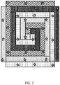
- Figure 7 shows four identical lighting devices of Figure 5 tessellated.
- Figure 8 shows a fourth example of lighting device which enables four identical coil shapes to be formed while also maintaining a regular grid of lighting elements according to the invention.
- the design has the same overall shape as the design of Figures 3 and 5 , namely a square/rectangular coil structure.
- the straight sections 10a, 10b, 10c, 10d have a width which varies between a narrower width w1 and a wider width w2, with the lighting elements 12 positioned at the portions with a wider width.
- the straight sections are still straight in the sense that they extend along a straight axial direction.
- the straight sections may be considered to have a central axis 80 (even though they are not symmetric about this axis), and each straight section has narrow parts and wide parts.
- the narrow parts mean that the central axis 80 is outside the area of the section, whereas the wide parts mean that the central axis is within the area of the section.
- the lighting elements 12 can be positioned along the central axis 80. In this way, the lighting elements can be positioned in the manner shown in Figure 6 .
- the wider portions of one straight section mate with a narrower portion of a laterally adjacent winding of a different coil when the multiple coils are tessellated.
- each straight section is straight, and the other edge forms a profiled edge.
- the narrower width portions may be formed by indents along the profiled edge, wherein the indents for one set of alternate straight sections are at an inside edge and the indents for the other set of alternate straight sections are at an outside edge. Accordingly, the straight edges for one set of alternate straight sections are at an outside edge and the the straight edges for the other set of alternate straight sections are at an inside edge.
- Figure 9 shows two identical lighting devices of Figure 8 interleaved with each other. This produces a device with double the light output flux of the device of Figure 8 , in a modular way.
- the coils are spaced apart (with a 180 degree rotational shift) to make the combined grid of lighting elements evenly distributed.
- a lighting product may use 1, 2, 3 or all four of the lighting devices of Figure 8 .
- Figure 10 shows four identical lighting devices of Figure 8 tessellated, which shows how the four lighting devices would be manufactured.
- the finite width of the coils means that they do not converge to a perfect point.
- there is a small star of PCB board in the center which is not needed in any of the carrier boards, but equally the innermost part of the coil shape could be designed so that all four coils tessellate fully.
- the outer shape of the four tessellated coils is generally square, with almost no wastage from a square board.
- the designs shown may be stretched along one axis, thereby converting all square profiles into rectangular profiles.
- the individual boards will no longer be identical, but they will perform an identical function.
- the individual boards will then be scalar stretched versions of each other.
- a method of manufacturing a lighting device according to the invention is shown in Figure 11 .
- the method comprises:
- Figure 12 shows a stretched version of the design of Figure 10 and also shows two of the individual coils.
- the shapes are no longer identical, but they are topologically "similar” in that they are scalar stretched versions of each other, and they achieve the same function.
- Each gives a regular rectangular array of lighting elements.
- the examples above using curved spirals enable any number of interleaved carrier boards to be formed.
- the square based angular design allows two or four interleaved carrier boards, as a result of the rotational symmetry of order 4.
- a hexagonal based design may also be used.
- the invention is of interest for general illumination luminaires, with a square or circular shape, such as troffers and downlights.
- the lighting elements are preferably solid state lighting elements, most preferably LEDs.
- the outer dimensions of the coil shaped carrier board may have various different values to fit many different types of lighting device.
- Downlight modules typically have a 60 mm diameter. Troffers are typically close to 300 x 1200 mm or 600 x 600 mm in some geographic regions, and the light engine is typically 200 to 400 mm square. Light troffers may however, be around 600 x 1200 mm (2 feet by 4 feet) in particular in the US, and the light engines may then be larger.
- the spacing of the LEDs depends on the height of the diffuser over the LEDs. Typical values are 1 to 5 cm. When the LEDs are combined with optical elements to improve the beam spreading, or when the troffer is quite deep, larger spacings can be used, such as 5 to 10 cm. The invention is particularly useful for large spacings, because then there is more unused PCB area in the conventional solution.
- the coil width w is for example around 10 mm or less, with a typical LED spacing of around 35 to 40 mm. For four coils, this gives a coil spacing d of 40 mm. Combined with the indentations, the narrowest part becomes about 5 mm.
- the tracks may need about 2 mm spacing from the board edge. This means that more than 40 mm LED spacing is desired to allow for an electrically safe product in case of four spirals. This is not a fundamental limit, because the electrical safety may also be solved by a different electrical layout (for example not all LEDs in series), which would allow for a lower string voltage and a smaller safety margin on the edge.
- the LED spacing is typically more than 5 mm times the number of spirals, and more than 10 mm times the number of spirals when indentations are used.
Claims (4)
- Beleuchtungsvorrichtung, umfassend:eine Trägerleiterplatte (10); undeinen Array von Beleuchtungselementen (12), der auf der Trägerleitplatte (10) montiert ist,wobei die Trägerleiterplatte (10) eine Spulenform mit zumindest zwei zusammenlaufenden Windungen hat, die der Trägerleiterplatte (10) erlaubt, mit einer oder mehr identisch geformten oder ähnlich geformten anderen Trägerleiterplatten mit ineinander verzahnten Windungen mosaikartig angeordnet zu sein,wobei die Windungen gerade Abschnitte (10a, 10b, 10c, 10d) mit einem 90-Grad Winkel zwischen den aneinandergrenzenden Abschnitten entlang der Spule umfassen, wobei die rechtwinklige Beabstandung zwischen aneinandergrenzenden Windungen eine Konstante ist,wobei die geraden Abschnitte (10a, 10b, 10c, 10d) eine Breite aufweisen, die zwischen einer schmaleren Breite (w1) und einer breiteren Breite (w2) variiert, wobei die Beleuchtungselemente (12) bei den Bereichen mit einer breiteren Breite (w2) positioniert sind, und der Array von Beleuchtungselementen (12) ein regelmäßiges Quadrat oder rechteckiges Gitter bilden, undwobei die schmalere Breitenbereiche durch Eindellungen gebildet sind, wobei die Eindellungen für einen Satz von abwechselnd geraden Abschnitten an einer Innenkante sind und die Eindellungen für den anderen Satz von abwechselnd geraden Abschnitten an einer Außenkante sind.
- Beleuchtungsvorrichtung nach Anspruch 1, wobei die Trägerleiterplatte (10) mit drei identischen oder ähnlichen Trägerleiterplatten mit ineinander verzahnten Windungen mosaikartig angeordnet werden kann.
- Beleuchtungsvorrichtung nach einem der vorstehenden Ansprüche, wobei ein elektrischer Verbinder am äußersten Ende der Spulenform oder an einer zwischenliegenden Position entlang der Spulenform bereitgestellt ist.
- Verfahren zur Herstellung einer Beleuchtungsvorrichtung, das Verfahren umfassend die Schritte zum:- Bilden eines Arrays von Beleuchtungselementen (12) auf einer Trägerleiterplatte (10) und- Trennen der Trägerleiterplatte (10) in zumindest zwei identisch geformte oder ähnlich geformte Abschnitte, wobei der Array von Beleuchtungselementen auf jedem Abschnitt ein regelmäßiges Quadrat oder rechteckiges Gitter bildet,wobei jeder Abschnitt eine Spulenform mit mehreren zusammenlaufenden Windungen aufweist, wobei die Windungen vor der Trennung ineinander verzahnt sind,
wobei die Windungen gerade Abschnitte (10a, 10b, 10c, 10d) mit einem 90-Grad Winkel zwischen den aneinandergrenzenden Abschnitten entlang der Spule umfassen, wobei die rechtwinklige Beabstandung zwischen aneinandergrenzenden Windungen eine Konstante ist,
wobei die geraden Abschnitte (10a, 10b, 10c, 10d) eine Breite aufweisen, die zwischen einer schmaleren Breite (w1) und einer breiteren Breite (w2) variiert, wobei die Beleuchtungselemente (12) bei den Bereichen mit einer breiteren Breite (w2) positioniert sind, und
wobei die schmaleren Breitenbereiche durch Eindellungen gebildet sind, wobei die Eindellungen für einen Satz von abwechselnd geraden Abschnitten an einer Innenkante sind und die Eindellungen für den anderen Satz von abwechselnd geraden Abschnitten an einer Außenkante sind.
Applications Claiming Priority (2)
| Application Number | Priority Date | Filing Date | Title |
|---|---|---|---|
| EP15181765 | 2015-08-20 | ||
| PCT/EP2016/069418 WO2017029286A1 (en) | 2015-08-20 | 2016-08-16 | Board mounted led array |
Publications (2)
| Publication Number | Publication Date |
|---|---|
| EP3338022A1 EP3338022A1 (de) | 2018-06-27 |
| EP3338022B1 true EP3338022B1 (de) | 2019-01-30 |
Family
ID=53887008
Family Applications (1)
| Application Number | Title | Priority Date | Filing Date |
|---|---|---|---|
| EP16753351.2A Not-in-force EP3338022B1 (de) | 2015-08-20 | 2016-08-16 | Leiterplattenmontierter led-array |
Country Status (5)
| Country | Link |
|---|---|
| US (1) | US10222010B2 (de) |
| EP (1) | EP3338022B1 (de) |
| JP (1) | JP2018525792A (de) |
| CN (1) | CN107923581A (de) |
| WO (1) | WO2017029286A1 (de) |
Families Citing this family (3)
| Publication number | Priority date | Publication date | Assignee | Title |
|---|---|---|---|---|
| CN112020772A (zh) * | 2018-04-28 | 2020-12-01 | 深圳市柔宇科技股份有限公司 | 基板、电子装置、接合结构及其接合方法 |
| USD900356S1 (en) * | 2018-08-06 | 2020-10-27 | Shenzhen Smart & Green Technology Co., Ltd. | LED light |
| JP2023509990A (ja) * | 2020-01-20 | 2023-03-10 | シグニファイ ホールディング ビー ヴィ | 同一の湾曲ledモジュールを有する照明器具、及び前記照明器具に適したledモジュール |
Family Cites Families (14)
| Publication number | Priority date | Publication date | Assignee | Title |
|---|---|---|---|---|
| ATE455273T1 (de) * | 2006-04-25 | 2010-01-15 | Koninkl Philips Electronics Nv | Grossflächiges led-array und herstellungsverfahren dafür |
| KR100980365B1 (ko) * | 2008-08-25 | 2010-09-06 | 주식회사 웰라이트 | 바 타입의 엘이디 조명 장치 |
| US7869270B2 (en) * | 2008-12-29 | 2011-01-11 | Macronix International Co., Ltd. | Set algorithm for phase change memory cell |
| TWM366267U (en) * | 2009-04-16 | 2009-10-01 | Taiwan Oasis Technology Co Ltd | LED substrate |
| CN101834175B (zh) | 2010-05-13 | 2015-07-15 | 中节能晶和照明有限公司 | Led照明cob封装结构以及球泡 |
| US8307547B1 (en) | 2012-01-16 | 2012-11-13 | Indak Manufacturing Corp. | Method of manufacturing a circuit board with light emitting diodes |
| CN202841695U (zh) | 2012-10-24 | 2013-03-27 | 盱眙凯亿电子材料有限公司 | Led灯用螺旋型电路板 |
| WO2014079220A1 (zh) * | 2012-11-22 | 2014-05-30 | Huang Kuo-Hao | 一种电路板及广角照射的led灯 |
| CN103016977B (zh) * | 2012-11-22 | 2015-08-26 | 鹤山健豪灯饰企业有限公司 | 一种广角照射的led灯 |
| US9482410B2 (en) | 2012-12-11 | 2016-11-01 | Samsung Electronics Co., Ltd. | Light emitting module and surface lighting device having the same |
| KR102098590B1 (ko) | 2012-12-11 | 2020-04-09 | 삼성전자주식회사 | 발광모듈 및 이를 구비한 면 조명장치 |
| KR200471587Y1 (ko) * | 2013-10-07 | 2014-03-04 | 권일봉 | 평면 나선형 pcb가 구비된 led 등기구 |
| CN203743877U (zh) | 2013-12-26 | 2014-07-30 | 上海顿格电子贸易有限公司 | 螺旋状发光二极管灯丝 |
| CN204062571U (zh) | 2014-08-01 | 2014-12-31 | 王定锋 | 一种螺旋状灯丝的led灯泡模组 |
-
2016
- 2016-08-16 US US15/753,009 patent/US10222010B2/en not_active Expired - Fee Related
- 2016-08-16 JP JP2018509556A patent/JP2018525792A/ja active Pending
- 2016-08-16 EP EP16753351.2A patent/EP3338022B1/de not_active Not-in-force
- 2016-08-16 WO PCT/EP2016/069418 patent/WO2017029286A1/en active Application Filing
- 2016-08-16 CN CN201680048309.5A patent/CN107923581A/zh active Pending
Non-Patent Citations (1)
| Title |
|---|
| None * |
Also Published As
| Publication number | Publication date |
|---|---|
| EP3338022A1 (de) | 2018-06-27 |
| WO2017029286A1 (en) | 2017-02-23 |
| US10222010B2 (en) | 2019-03-05 |
| US20180306391A1 (en) | 2018-10-25 |
| JP2018525792A (ja) | 2018-09-06 |
| CN107923581A (zh) | 2018-04-17 |
Similar Documents
| Publication | Publication Date | Title |
|---|---|---|
| EP3338022B1 (de) | Leiterplattenmontierter led-array | |
| US9869456B2 (en) | Fixture design for flexible LED circuit boards | |
| KR20130048241A (ko) | Led 배선 기판 및 광 조사 장치 | |
| US20120273808A1 (en) | Led array module and fabrication method thereof | |
| JP3141579U (ja) | Led照明器具 | |
| US9587808B2 (en) | Fixture design for flexible LED circuit boards | |
| WO2016018843A1 (en) | Led lighting system incorporating folded light sheets | |
| EP2890925B1 (de) | Modularer led-anordnungsraster und verfahren zur bereitstellung eines derartigen modularen led-anordnungsrasters | |
| JPWO2017115862A1 (ja) | Led照明装置 | |
| JP5854530B2 (ja) | Ledアレイのための低コスト多機能ヒートシンク | |
| JP6038047B2 (ja) | 照明製品のための多機能ヒートシンク | |
| US8840271B2 (en) | In-plane bent printed circuit boards | |
| EP2873310B1 (de) | Optimierte leiterplatte | |
| WO2014155347A1 (en) | Printed circuit board for a light emitting diode module | |
| KR101871325B1 (ko) | 천장마감형 엘이디조명장치 | |
| EP3655696A1 (de) | Lichtemittierendes modul | |
| JP3133397U (ja) | Led照明具の発光ダイオード配列構造 | |
| WO2020089146A1 (en) | Light-emitting device with solid-state light sources | |
| JP2014143111A (ja) | Ledモジュール | |
| JP2012155872A (ja) | Ledランプ | |
| CN111520689B (zh) | 具有改进的印刷电路板的光引擎 | |
| US11906118B2 (en) | Foldable light generating device | |
| US20220159837A1 (en) | Interconnectable circuit boards adapted for three-dimensional constructions as lighting sources | |
| WO2016055318A1 (en) | Lighting device | |
| JP2019102359A (ja) | 光源ユニット及び照明装置 |
Legal Events
| Date | Code | Title | Description |
|---|---|---|---|
| STAA | Information on the status of an ep patent application or granted ep patent |
Free format text: STATUS: THE INTERNATIONAL PUBLICATION HAS BEEN MADE |
|
| PUAI | Public reference made under article 153(3) epc to a published international application that has entered the european phase |
Free format text: ORIGINAL CODE: 0009012 |
|
| STAA | Information on the status of an ep patent application or granted ep patent |
Free format text: STATUS: REQUEST FOR EXAMINATION WAS MADE |
|
| 17P | Request for examination filed |
Effective date: 20180320 |
|
| AK | Designated contracting states |
Kind code of ref document: A1 Designated state(s): AL AT BE BG CH CY CZ DE DK EE ES FI FR GB GR HR HU IE IS IT LI LT LU LV MC MK MT NL NO PL PT RO RS SE SI SK SM TR |
|
| AX | Request for extension of the european patent |
Extension state: BA ME |
|
| GRAP | Despatch of communication of intention to grant a patent |
Free format text: ORIGINAL CODE: EPIDOSNIGR1 |
|
| STAA | Information on the status of an ep patent application or granted ep patent |
Free format text: STATUS: GRANT OF PATENT IS INTENDED |
|
| DAV | Request for validation of the european patent (deleted) | ||
| DAX | Request for extension of the european patent (deleted) | ||
| INTG | Intention to grant announced |
Effective date: 20180816 |
|
| RAP1 | Party data changed (applicant data changed or rights of an application transferred) |
Owner name: PHILIPS LIGHTING HOLDING B.V. |
|
| GRAS | Grant fee paid |
Free format text: ORIGINAL CODE: EPIDOSNIGR3 |
|
| GRAA | (expected) grant |
Free format text: ORIGINAL CODE: 0009210 |
|
| STAA | Information on the status of an ep patent application or granted ep patent |
Free format text: STATUS: THE PATENT HAS BEEN GRANTED |
|
| AK | Designated contracting states |
Kind code of ref document: B1 Designated state(s): AL AT BE BG CH CY CZ DE DK EE ES FI FR GB GR HR HU IE IS IT LI LT LU LV MC MK MT NL NO PL PT RO RS SE SI SK SM TR |
|
| REG | Reference to a national code |
Ref country code: GB Ref legal event code: FG4D |
|
| REG | Reference to a national code |
Ref country code: CH Ref legal event code: EP |
|
| REG | Reference to a national code |
Ref country code: AT Ref legal event code: REF Ref document number: 1093560 Country of ref document: AT Kind code of ref document: T Effective date: 20190215 |
|
| REG | Reference to a national code |
Ref country code: IE Ref legal event code: FG4D |
|
| REG | Reference to a national code |
Ref country code: DE Ref legal event code: R096 Ref document number: 602016009711 Country of ref document: DE |
|
| RAP2 | Party data changed (patent owner data changed or rights of a patent transferred) |
Owner name: SIGNIFY HOLDING B.V. |
|
| REG | Reference to a national code |
Ref country code: LT Ref legal event code: MG4D |
|
| REG | Reference to a national code |
Ref country code: NL Ref legal event code: MP Effective date: 20190130 |
|
| PG25 | Lapsed in a contracting state [announced via postgrant information from national office to epo] |
Ref country code: FI Free format text: LAPSE BECAUSE OF FAILURE TO SUBMIT A TRANSLATION OF THE DESCRIPTION OR TO PAY THE FEE WITHIN THE PRESCRIBED TIME-LIMIT Effective date: 20190130 Ref country code: PL Free format text: LAPSE BECAUSE OF FAILURE TO SUBMIT A TRANSLATION OF THE DESCRIPTION OR TO PAY THE FEE WITHIN THE PRESCRIBED TIME-LIMIT Effective date: 20190130 Ref country code: PT Free format text: LAPSE BECAUSE OF FAILURE TO SUBMIT A TRANSLATION OF THE DESCRIPTION OR TO PAY THE FEE WITHIN THE PRESCRIBED TIME-LIMIT Effective date: 20190530 Ref country code: NO Free format text: LAPSE BECAUSE OF FAILURE TO SUBMIT A TRANSLATION OF THE DESCRIPTION OR TO PAY THE FEE WITHIN THE PRESCRIBED TIME-LIMIT Effective date: 20190430 Ref country code: NL Free format text: LAPSE BECAUSE OF FAILURE TO SUBMIT A TRANSLATION OF THE DESCRIPTION OR TO PAY THE FEE WITHIN THE PRESCRIBED TIME-LIMIT Effective date: 20190130 Ref country code: SE Free format text: LAPSE BECAUSE OF FAILURE TO SUBMIT A TRANSLATION OF THE DESCRIPTION OR TO PAY THE FEE WITHIN THE PRESCRIBED TIME-LIMIT Effective date: 20190130 Ref country code: ES Free format text: LAPSE BECAUSE OF FAILURE TO SUBMIT A TRANSLATION OF THE DESCRIPTION OR TO PAY THE FEE WITHIN THE PRESCRIBED TIME-LIMIT Effective date: 20190130 Ref country code: LT Free format text: LAPSE BECAUSE OF FAILURE TO SUBMIT A TRANSLATION OF THE DESCRIPTION OR TO PAY THE FEE WITHIN THE PRESCRIBED TIME-LIMIT Effective date: 20190130 |
|
| REG | Reference to a national code |
Ref country code: AT Ref legal event code: MK05 Ref document number: 1093560 Country of ref document: AT Kind code of ref document: T Effective date: 20190130 |
|
| PG25 | Lapsed in a contracting state [announced via postgrant information from national office to epo] |
Ref country code: HR Free format text: LAPSE BECAUSE OF FAILURE TO SUBMIT A TRANSLATION OF THE DESCRIPTION OR TO PAY THE FEE WITHIN THE PRESCRIBED TIME-LIMIT Effective date: 20190130 Ref country code: GR Free format text: LAPSE BECAUSE OF FAILURE TO SUBMIT A TRANSLATION OF THE DESCRIPTION OR TO PAY THE FEE WITHIN THE PRESCRIBED TIME-LIMIT Effective date: 20190501 Ref country code: RS Free format text: LAPSE BECAUSE OF FAILURE TO SUBMIT A TRANSLATION OF THE DESCRIPTION OR TO PAY THE FEE WITHIN THE PRESCRIBED TIME-LIMIT Effective date: 20190130 Ref country code: IS Free format text: LAPSE BECAUSE OF FAILURE TO SUBMIT A TRANSLATION OF THE DESCRIPTION OR TO PAY THE FEE WITHIN THE PRESCRIBED TIME-LIMIT Effective date: 20190530 Ref country code: BG Free format text: LAPSE BECAUSE OF FAILURE TO SUBMIT A TRANSLATION OF THE DESCRIPTION OR TO PAY THE FEE WITHIN THE PRESCRIBED TIME-LIMIT Effective date: 20190430 Ref country code: LV Free format text: LAPSE BECAUSE OF FAILURE TO SUBMIT A TRANSLATION OF THE DESCRIPTION OR TO PAY THE FEE WITHIN THE PRESCRIBED TIME-LIMIT Effective date: 20190130 |
|
| PG25 | Lapsed in a contracting state [announced via postgrant information from national office to epo] |
Ref country code: EE Free format text: LAPSE BECAUSE OF FAILURE TO SUBMIT A TRANSLATION OF THE DESCRIPTION OR TO PAY THE FEE WITHIN THE PRESCRIBED TIME-LIMIT Effective date: 20190130 Ref country code: SK Free format text: LAPSE BECAUSE OF FAILURE TO SUBMIT A TRANSLATION OF THE DESCRIPTION OR TO PAY THE FEE WITHIN THE PRESCRIBED TIME-LIMIT Effective date: 20190130 Ref country code: AL Free format text: LAPSE BECAUSE OF FAILURE TO SUBMIT A TRANSLATION OF THE DESCRIPTION OR TO PAY THE FEE WITHIN THE PRESCRIBED TIME-LIMIT Effective date: 20190130 Ref country code: IT Free format text: LAPSE BECAUSE OF FAILURE TO SUBMIT A TRANSLATION OF THE DESCRIPTION OR TO PAY THE FEE WITHIN THE PRESCRIBED TIME-LIMIT Effective date: 20190130 Ref country code: DK Free format text: LAPSE BECAUSE OF FAILURE TO SUBMIT A TRANSLATION OF THE DESCRIPTION OR TO PAY THE FEE WITHIN THE PRESCRIBED TIME-LIMIT Effective date: 20190130 Ref country code: CZ Free format text: LAPSE BECAUSE OF FAILURE TO SUBMIT A TRANSLATION OF THE DESCRIPTION OR TO PAY THE FEE WITHIN THE PRESCRIBED TIME-LIMIT Effective date: 20190130 Ref country code: RO Free format text: LAPSE BECAUSE OF FAILURE TO SUBMIT A TRANSLATION OF THE DESCRIPTION OR TO PAY THE FEE WITHIN THE PRESCRIBED TIME-LIMIT Effective date: 20190130 |
|
| PGFP | Annual fee paid to national office [announced via postgrant information from national office to epo] |
Ref country code: FR Payment date: 20190827 Year of fee payment: 4 |
|
| REG | Reference to a national code |
Ref country code: DE Ref legal event code: R097 Ref document number: 602016009711 Country of ref document: DE |
|
| PG25 | Lapsed in a contracting state [announced via postgrant information from national office to epo] |
Ref country code: SM Free format text: LAPSE BECAUSE OF FAILURE TO SUBMIT A TRANSLATION OF THE DESCRIPTION OR TO PAY THE FEE WITHIN THE PRESCRIBED TIME-LIMIT Effective date: 20190130 |
|
| PLBE | No opposition filed within time limit |
Free format text: ORIGINAL CODE: 0009261 |
|
| STAA | Information on the status of an ep patent application or granted ep patent |
Free format text: STATUS: NO OPPOSITION FILED WITHIN TIME LIMIT |
|
| PG25 | Lapsed in a contracting state [announced via postgrant information from national office to epo] |
Ref country code: AT Free format text: LAPSE BECAUSE OF FAILURE TO SUBMIT A TRANSLATION OF THE DESCRIPTION OR TO PAY THE FEE WITHIN THE PRESCRIBED TIME-LIMIT Effective date: 20190130 |
|
| 26N | No opposition filed |
Effective date: 20191031 |
|
| PGFP | Annual fee paid to national office [announced via postgrant information from national office to epo] |
Ref country code: DE Payment date: 20191031 Year of fee payment: 4 |
|
| PG25 | Lapsed in a contracting state [announced via postgrant information from national office to epo] |
Ref country code: TR Free format text: LAPSE BECAUSE OF FAILURE TO SUBMIT A TRANSLATION OF THE DESCRIPTION OR TO PAY THE FEE WITHIN THE PRESCRIBED TIME-LIMIT Effective date: 20190130 |
|
| PG25 | Lapsed in a contracting state [announced via postgrant information from national office to epo] |
Ref country code: LU Free format text: LAPSE BECAUSE OF NON-PAYMENT OF DUE FEES Effective date: 20190816 Ref country code: CH Free format text: LAPSE BECAUSE OF NON-PAYMENT OF DUE FEES Effective date: 20190831 Ref country code: MC Free format text: LAPSE BECAUSE OF FAILURE TO SUBMIT A TRANSLATION OF THE DESCRIPTION OR TO PAY THE FEE WITHIN THE PRESCRIBED TIME-LIMIT Effective date: 20190130 Ref country code: LI Free format text: LAPSE BECAUSE OF NON-PAYMENT OF DUE FEES Effective date: 20190831 |
|
| REG | Reference to a national code |
Ref country code: BE Ref legal event code: MM Effective date: 20190831 |
|
| PG25 | Lapsed in a contracting state [announced via postgrant information from national office to epo] |
Ref country code: IE Free format text: LAPSE BECAUSE OF NON-PAYMENT OF DUE FEES Effective date: 20190816 |
|
| PG25 | Lapsed in a contracting state [announced via postgrant information from national office to epo] |
Ref country code: BE Free format text: LAPSE BECAUSE OF NON-PAYMENT OF DUE FEES Effective date: 20190831 |
|
| REG | Reference to a national code |
Ref country code: DE Ref legal event code: R119 Ref document number: 602016009711 Country of ref document: DE |
|
| GBPC | Gb: european patent ceased through non-payment of renewal fee |
Effective date: 20200816 |
|
| PG25 | Lapsed in a contracting state [announced via postgrant information from national office to epo] |
Ref country code: CY Free format text: LAPSE BECAUSE OF FAILURE TO SUBMIT A TRANSLATION OF THE DESCRIPTION OR TO PAY THE FEE WITHIN THE PRESCRIBED TIME-LIMIT Effective date: 20190130 |
|
| PG25 | Lapsed in a contracting state [announced via postgrant information from national office to epo] |
Ref country code: HU Free format text: LAPSE BECAUSE OF FAILURE TO SUBMIT A TRANSLATION OF THE DESCRIPTION OR TO PAY THE FEE WITHIN THE PRESCRIBED TIME-LIMIT; INVALID AB INITIO Effective date: 20160816 Ref country code: DE Free format text: LAPSE BECAUSE OF NON-PAYMENT OF DUE FEES Effective date: 20210302 Ref country code: MT Free format text: LAPSE BECAUSE OF FAILURE TO SUBMIT A TRANSLATION OF THE DESCRIPTION OR TO PAY THE FEE WITHIN THE PRESCRIBED TIME-LIMIT Effective date: 20190130 Ref country code: FR Free format text: LAPSE BECAUSE OF NON-PAYMENT OF DUE FEES Effective date: 20200831 |
|
| PG25 | Lapsed in a contracting state [announced via postgrant information from national office to epo] |
Ref country code: GB Free format text: LAPSE BECAUSE OF NON-PAYMENT OF DUE FEES Effective date: 20200816 |
|
| PG25 | Lapsed in a contracting state [announced via postgrant information from national office to epo] |
Ref country code: SI Free format text: LAPSE BECAUSE OF FAILURE TO SUBMIT A TRANSLATION OF THE DESCRIPTION OR TO PAY THE FEE WITHIN THE PRESCRIBED TIME-LIMIT Effective date: 20190130 |
|
| PG25 | Lapsed in a contracting state [announced via postgrant information from national office to epo] |
Ref country code: MK Free format text: LAPSE BECAUSE OF FAILURE TO SUBMIT A TRANSLATION OF THE DESCRIPTION OR TO PAY THE FEE WITHIN THE PRESCRIBED TIME-LIMIT Effective date: 20190130 |