EP3336890B1 - Leistungshalbleitermodule mit schutzbeschichtung und verfahren zu deren herstellung - Google Patents
Leistungshalbleitermodule mit schutzbeschichtung und verfahren zu deren herstellung Download PDFInfo
- Publication number
- EP3336890B1 EP3336890B1 EP17206860.3A EP17206860A EP3336890B1 EP 3336890 B1 EP3336890 B1 EP 3336890B1 EP 17206860 A EP17206860 A EP 17206860A EP 3336890 B1 EP3336890 B1 EP 3336890B1
- Authority
- EP
- European Patent Office
- Prior art keywords
- molded plastic
- plastic body
- coating
- terminals
- semiconductor package
- Prior art date
- Legal status (The legal status is an assumption and is not a legal conclusion. Google has not performed a legal analysis and makes no representation as to the accuracy of the status listed.)
- Active
Links
Images



Classifications
-
- H—ELECTRICITY
- H10—SEMICONDUCTOR DEVICES; ELECTRIC SOLID-STATE DEVICES NOT OTHERWISE PROVIDED FOR
- H10W—GENERIC PACKAGES, INTERCONNECTIONS, CONNECTORS OR OTHER CONSTRUCTIONAL DETAILS OF DEVICES COVERED BY CLASS H10
- H10W74/00—Encapsulations, e.g. protective coatings
- H10W74/40—Encapsulations, e.g. protective coatings characterised by their materials
- H10W74/47—Encapsulations, e.g. protective coatings characterised by their materials comprising organic materials, e.g. plastics or resins
-
- H—ELECTRICITY
- H10—SEMICONDUCTOR DEVICES; ELECTRIC SOLID-STATE DEVICES NOT OTHERWISE PROVIDED FOR
- H10W—GENERIC PACKAGES, INTERCONNECTIONS, CONNECTORS OR OTHER CONSTRUCTIONAL DETAILS OF DEVICES COVERED BY CLASS H10
- H10W74/00—Encapsulations, e.g. protective coatings
- H10W74/10—Encapsulations, e.g. protective coatings characterised by their shape or disposition
- H10W74/131—Encapsulations, e.g. protective coatings characterised by their shape or disposition the semiconductor body being only partially enclosed
- H10W74/137—Encapsulations, e.g. protective coatings characterised by their shape or disposition the semiconductor body being only partially enclosed the encapsulations being directly on the semiconductor body
-
- C—CHEMISTRY; METALLURGY
- C09—DYES; PAINTS; POLISHES; NATURAL RESINS; ADHESIVES; COMPOSITIONS NOT OTHERWISE PROVIDED FOR; APPLICATIONS OF MATERIALS NOT OTHERWISE PROVIDED FOR
- C09K—MATERIALS FOR MISCELLANEOUS APPLICATIONS, NOT PROVIDED FOR ELSEWHERE
- C09K21/00—Fireproofing materials
- C09K21/06—Organic materials
-
- H—ELECTRICITY
- H10—SEMICONDUCTOR DEVICES; ELECTRIC SOLID-STATE DEVICES NOT OTHERWISE PROVIDED FOR
- H10W—GENERIC PACKAGES, INTERCONNECTIONS, CONNECTORS OR OTHER CONSTRUCTIONAL DETAILS OF DEVICES COVERED BY CLASS H10
- H10W74/00—Encapsulations, e.g. protective coatings
-
- H—ELECTRICITY
- H10—SEMICONDUCTOR DEVICES; ELECTRIC SOLID-STATE DEVICES NOT OTHERWISE PROVIDED FOR
- H10W—GENERIC PACKAGES, INTERCONNECTIONS, CONNECTORS OR OTHER CONSTRUCTIONAL DETAILS OF DEVICES COVERED BY CLASS H10
- H10W74/00—Encapsulations, e.g. protective coatings
- H10W74/01—Manufacture or treatment
-
- H—ELECTRICITY
- H10—SEMICONDUCTOR DEVICES; ELECTRIC SOLID-STATE DEVICES NOT OTHERWISE PROVIDED FOR
- H10W—GENERIC PACKAGES, INTERCONNECTIONS, CONNECTORS OR OTHER CONSTRUCTIONAL DETAILS OF DEVICES COVERED BY CLASS H10
- H10W74/00—Encapsulations, e.g. protective coatings
- H10W74/10—Encapsulations, e.g. protective coatings characterised by their shape or disposition
- H10W74/111—Encapsulations, e.g. protective coatings characterised by their shape or disposition the semiconductor body being completely enclosed
-
- H—ELECTRICITY
- H10—SEMICONDUCTOR DEVICES; ELECTRIC SOLID-STATE DEVICES NOT OTHERWISE PROVIDED FOR
- H10W—GENERIC PACKAGES, INTERCONNECTIONS, CONNECTORS OR OTHER CONSTRUCTIONAL DETAILS OF DEVICES COVERED BY CLASS H10
- H10W74/00—Encapsulations, e.g. protective coatings
- H10W74/10—Encapsulations, e.g. protective coatings characterised by their shape or disposition
- H10W74/111—Encapsulations, e.g. protective coatings characterised by their shape or disposition the semiconductor body being completely enclosed
- H10W74/121—Encapsulations, e.g. protective coatings characterised by their shape or disposition the semiconductor body being completely enclosed by multiple encapsulations, e.g. by a thin protective coating and a thick encapsulation
-
- H—ELECTRICITY
- H10—SEMICONDUCTOR DEVICES; ELECTRIC SOLID-STATE DEVICES NOT OTHERWISE PROVIDED FOR
- H10W—GENERIC PACKAGES, INTERCONNECTIONS, CONNECTORS OR OTHER CONSTRUCTIONAL DETAILS OF DEVICES COVERED BY CLASS H10
- H10W74/00—Encapsulations, e.g. protective coatings
- H10W74/10—Encapsulations, e.g. protective coatings characterised by their shape or disposition
- H10W74/111—Encapsulations, e.g. protective coatings characterised by their shape or disposition the semiconductor body being completely enclosed
- H10W74/127—Encapsulations, e.g. protective coatings characterised by their shape or disposition the semiconductor body being completely enclosed characterised by arrangements for sealing or adhesion
-
- H—ELECTRICITY
- H10—SEMICONDUCTOR DEVICES; ELECTRIC SOLID-STATE DEVICES NOT OTHERWISE PROVIDED FOR
- H10W—GENERIC PACKAGES, INTERCONNECTIONS, CONNECTORS OR OTHER CONSTRUCTIONAL DETAILS OF DEVICES COVERED BY CLASS H10
- H10W74/00—Encapsulations, e.g. protective coatings
- H10W74/10—Encapsulations, e.g. protective coatings characterised by their shape or disposition
- H10W74/131—Encapsulations, e.g. protective coatings characterised by their shape or disposition the semiconductor body being only partially enclosed
-
- H—ELECTRICITY
- H10—SEMICONDUCTOR DEVICES; ELECTRIC SOLID-STATE DEVICES NOT OTHERWISE PROVIDED FOR
- H10W—GENERIC PACKAGES, INTERCONNECTIONS, CONNECTORS OR OTHER CONSTRUCTIONAL DETAILS OF DEVICES COVERED BY CLASS H10
- H10W74/00—Encapsulations, e.g. protective coatings
- H10W74/10—Encapsulations, e.g. protective coatings characterised by their shape or disposition
- H10W74/131—Encapsulations, e.g. protective coatings characterised by their shape or disposition the semiconductor body being only partially enclosed
- H10W74/147—Encapsulations, e.g. protective coatings characterised by their shape or disposition the semiconductor body being only partially enclosed the encapsulations being multilayered
-
- H—ELECTRICITY
- H10—SEMICONDUCTOR DEVICES; ELECTRIC SOLID-STATE DEVICES NOT OTHERWISE PROVIDED FOR
- H10W—GENERIC PACKAGES, INTERCONNECTIONS, CONNECTORS OR OTHER CONSTRUCTIONAL DETAILS OF DEVICES COVERED BY CLASS H10
- H10W76/00—Containers; Fillings or auxiliary members therefor; Seals
- H10W76/40—Fillings or auxiliary members in containers, e.g. centering rings
- H10W76/42—Fillings
-
- H—ELECTRICITY
- H10—SEMICONDUCTOR DEVICES; ELECTRIC SOLID-STATE DEVICES NOT OTHERWISE PROVIDED FOR
- H10W—GENERIC PACKAGES, INTERCONNECTIONS, CONNECTORS OR OTHER CONSTRUCTIONAL DETAILS OF DEVICES COVERED BY CLASS H10
- H10W42/00—Arrangements for protection of devices
-
- H—ELECTRICITY
- H10—SEMICONDUCTOR DEVICES; ELECTRIC SOLID-STATE DEVICES NOT OTHERWISE PROVIDED FOR
- H10W—GENERIC PACKAGES, INTERCONNECTIONS, CONNECTORS OR OTHER CONSTRUCTIONAL DETAILS OF DEVICES COVERED BY CLASS H10
- H10W90/00—Package configurations
- H10W90/701—Package configurations characterised by the relative positions of pads or connectors relative to package parts
- H10W90/721—Package configurations characterised by the relative positions of pads or connectors relative to package parts of bump connectors
- H10W90/724—Package configurations characterised by the relative positions of pads or connectors relative to package parts of bump connectors between a chip and a stacked insulating package substrate, interposer or RDL
-
- H—ELECTRICITY
- H10—SEMICONDUCTOR DEVICES; ELECTRIC SOLID-STATE DEVICES NOT OTHERWISE PROVIDED FOR
- H10W—GENERIC PACKAGES, INTERCONNECTIONS, CONNECTORS OR OTHER CONSTRUCTIONAL DETAILS OF DEVICES COVERED BY CLASS H10
- H10W90/00—Package configurations
- H10W90/701—Package configurations characterised by the relative positions of pads or connectors relative to package parts
- H10W90/721—Package configurations characterised by the relative positions of pads or connectors relative to package parts of bump connectors
- H10W90/726—Package configurations characterised by the relative positions of pads or connectors relative to package parts of bump connectors between a chip and a stacked lead frame, conducting package substrate or heat sink
-
- H—ELECTRICITY
- H10—SEMICONDUCTOR DEVICES; ELECTRIC SOLID-STATE DEVICES NOT OTHERWISE PROVIDED FOR
- H10W—GENERIC PACKAGES, INTERCONNECTIONS, CONNECTORS OR OTHER CONSTRUCTIONAL DETAILS OF DEVICES COVERED BY CLASS H10
- H10W90/00—Package configurations
- H10W90/701—Package configurations characterised by the relative positions of pads or connectors relative to package parts
- H10W90/751—Package configurations characterised by the relative positions of pads or connectors relative to package parts of bond wires
- H10W90/754—Package configurations characterised by the relative positions of pads or connectors relative to package parts of bond wires between a chip and a stacked insulating package substrate, interposer or RDL
-
- H—ELECTRICITY
- H10—SEMICONDUCTOR DEVICES; ELECTRIC SOLID-STATE DEVICES NOT OTHERWISE PROVIDED FOR
- H10W—GENERIC PACKAGES, INTERCONNECTIONS, CONNECTORS OR OTHER CONSTRUCTIONAL DETAILS OF DEVICES COVERED BY CLASS H10
- H10W90/00—Package configurations
- H10W90/701—Package configurations characterised by the relative positions of pads or connectors relative to package parts
- H10W90/751—Package configurations characterised by the relative positions of pads or connectors relative to package parts of bond wires
- H10W90/756—Package configurations characterised by the relative positions of pads or connectors relative to package parts of bond wires between a chip and a stacked lead frame, conducting package substrate or heat sink
-
- H—ELECTRICITY
- H10—SEMICONDUCTOR DEVICES; ELECTRIC SOLID-STATE DEVICES NOT OTHERWISE PROVIDED FOR
- H10W—GENERIC PACKAGES, INTERCONNECTIONS, CONNECTORS OR OTHER CONSTRUCTIONAL DETAILS OF DEVICES COVERED BY CLASS H10
- H10W90/00—Package configurations
- H10W90/701—Package configurations characterised by the relative positions of pads or connectors relative to package parts
- H10W90/761—Package configurations characterised by the relative positions of pads or connectors relative to package parts of strap connectors
- H10W90/764—Package configurations characterised by the relative positions of pads or connectors relative to package parts of strap connectors between a chip and a stacked insulating package substrate, interposer or RDL
-
- H—ELECTRICITY
- H10—SEMICONDUCTOR DEVICES; ELECTRIC SOLID-STATE DEVICES NOT OTHERWISE PROVIDED FOR
- H10W—GENERIC PACKAGES, INTERCONNECTIONS, CONNECTORS OR OTHER CONSTRUCTIONAL DETAILS OF DEVICES COVERED BY CLASS H10
- H10W90/00—Package configurations
- H10W90/701—Package configurations characterised by the relative positions of pads or connectors relative to package parts
- H10W90/761—Package configurations characterised by the relative positions of pads or connectors relative to package parts of strap connectors
- H10W90/766—Package configurations characterised by the relative positions of pads or connectors relative to package parts of strap connectors between a chip and a stacked lead frame, conducting package substrate or heat sink
Definitions
- the present application relates to power semiconductor modules, in particular power semiconductor modules which must satisfy a plurality of predetermined electrical, mechanical, chemical and/or environmental requirements.
- Power semiconductor modules typically include a molded plastic body such as a plastic molding compound in which power semiconductor dies are embedded, or a plastic housing which covers the power semiconductor dies.
- package materials are epoxies used in transfer molding devices or as potting material in modules, silicone gel used as potting material in modules, and engineering plastics such as PBT (polybutylene terephthalate), PET (polyethylene terephthalate), polyamide, PPS (polyphenylene sulfide), etc. as housing/envelope materials.
- PBT polybutylene terephthalate
- PET polyethylene terephthalate
- polyamide polyamide
- PPS polyphenylene sulfide
- Such materials not only have to fulfil predetermined mechanical requirements (e.g. elongation at yield ⁇ 1%, preferred; electrical RTI ⁇ 140°C, mechanical RTI ⁇ 140°C), but also environmental (e.g.
- RoHS RoHS
- REACH fire and smoke
- UL94V0 UL94V0
- EN45545 including HL2 and R22
- electrical e.g. related standards: IEC60664, including CTI>400, 600
- chemical e.g. low content of solvable ions
- additives are typically used.
- Additives such as flame retardants, fibers, minerals and other chemicals often comprise the electrical characteristics of the package.
- dielectric strength of the molded plastic body may be weakened over a long lifetime by ions or interfaces introduced by additives. Insulating characteristics may be weakened especially in a humid environment, or in a salt mist or acidic gaseous atmosphere.
- the package terminals may corrode where contacted by the molded plastic body and corrosive by-products may propagate over the surface of insulating portions.
- Semiconductor characteristics may be influenced as well by ionic additives.
- the predetermined electrical requirement CTI comparativet index
- Document US 2003/0013235 A1 discloses a semiconductor package which meets a plurality of predetermined environmental requirements, the semiconductor package comprising: a semiconductor die embedded in or covered by a molded plastic body, the molded plastic body satisfying only a subset of the plurality of predetermined environmental requirements; a plurality of terminals protruding from the molded plastic body and electrically connected to the semiconductor die; and a coating applied to the molded plastic body, wherein the coating is applied to the molded plastic body at least in a region where the plurality of terminals protrude from the molded plastic body, including between adjacent ones of the terminals, the coating comprising a plastic material and satisfying each predetermined environmental requirement not satisfied by the molded plastic body.
- Document WO 2015/000591 A2 discloses a die interconnect system comprising a die having a plurality of connection pads, a heat generating element thermally isolated from the die, one or more leads extending from the die to the heat generating element, each lead having a metal core with a core diameter, a dielectric layer surrounding the metal core with a dielectric thickness, and an outer metal layer attached to ground, wherein one or more leads are exposed to ambient conditions and/or are convectively or contact cooled for at least a portion of their length to minimize heat transfer from the heat generating element to the die.
- Document US 5,164,816 A discloses an integrated circuit device wherein layer insulation is attained by at least one of (i) an insulator layer interposed between two adjacent conductor layers, and (ii) a surface protecting layer fixedly covering the surface of the semiconductor chip, each of the insulator layer and the surface protecting layer being made of a heat-resistant resin obtainable by heating a heat-resistant resin paste.
- Said paste consists essentially of a first organic liquid, a second organic liquid, a heat-resistant resin which is soluble in an organic liquid mixture consisting of the first organic liquid and the second organic liquid, and fine particles of a heat-resistant resin which is soluble in the first organic liquid but insoluble in the second organic liquid.
- the first organic liquid, the second organic liquid and the heat-resistant resin are brought into a solution in which the fine particles of a heat-resistant resin are dispersed.
- Document US 6,046,507A discloses a semiconductor package which meets a plurality of predetermined electrical, mechanical, chemical and/or environmental requirements, the semiconductor package comprising: a semiconductor die embedded in or covered by a molded plastic body, the molded plastic body comprising a flame-retardant material, and satisfying only a subset of the plurality of predetermined electrical, mechanical, chemical and/or environmental requirements; a plurality of terminals protruding from the molded plastic body and electrically connected to the semiconductor die; the coating comprising a plastic material and satisfying each predetermined electrical, mechanical, chemical and/or environmental requirement not satisfied by the molded plastic body.
- the semiconductor package comprises a semiconductor die embedded in or covered by a molded plastic body, the molded plastic body comprising a flame-retardant material, and satisfying only a subset of the plurality of predetermined electrical, mechanical, chemical and/or environmental requirements.
- the semiconductor package further comprises a plurality of terminals protruding from the molded plastic body and electrically connected to the semiconductor die, and a coating applied to the molded plastic body, wherein either the coating coats the molded plastic body completely, or the coating is applied to the molded plastic body only in a region where the plurality of terminals protrude from the molded plastic body, including between adjacent ones of the terminals.
- the coating comprises a plastic material and satisfies each predetermined electrical, mechanical, chemical and/or environmental requirement not satisfied by the molded plastic body.
- the molded plastic body achieves a first comparative tracking index value that does not fulfil the comparative tracking index requirements for the semiconductor package, and the coating achieves a second comparative tracking index value that is higher than the first comparative tracking index value of the molded plastic body and that fulfils the comparative tracking index requirements.
- the method comprises: applying a coating to the molded plastic body, wherein either the coating is applied to coat the molded plastic body completely, or the coating is applied to the molded plastic body only in a region where the plurality of terminals protrude from the molded plastic body, including between adjacent ones of the terminals, wherein the molded plastic body comprises a flame-retardant material; and embedding or covering a semiconductor die by the molded plastic body.
- the terminals protrude from the molded plastic body and are electrically connected to the semiconductor die.
- the molded plastic body satisfies only a subset of the plurality of predetermined electrical, mechanical, chemical and/or environmental requirements.
- the coating comprises a plastic material and satisfies each predetermined electrical, mechanical, chemical and/or environmental requirement not satisfied by the molded plastic body.
- the molded plastic body achieves a first comparative tracking index value that does not fulfil the comparative tracking index requirements for the semiconductor package, and the coating achieves a second comparative tracking index value that is higher than the first comparative tracking index value of the molded plastic body and that fulfils the comparative tracking index requirements.
- Embodiments described herein provide a power semiconductor package which meets a plurality of predetermined electrical, mechanical, chemical and/or environmental requirements.
- the semiconductor package includes a molded plastic body that satisfies only a subset of the plurality of predetermined electrical, mechanical, chemical and/or environmental requirements.
- the semiconductor package further includes a coating applied to at least part of the molded plastic body and optionally to part of the package terminals, the coating satisfying each predetermined electrical, mechanical, chemical and/or environmental requirement not satisfied by the molded plastic body.
- Figures 1 through 3 illustrate different embodiments of a semiconductor package which meets a plurality of predetermined electrical, mechanical, chemical and/or environmental requirements, and which includes one or more semiconductor dies 100 embedded in a molded plastic body 102.
- a plurality of terminals 104 protrude from the molded plastic body 102 and are electrically connected to the semiconductor die 100 e.g. as leads of a leadframe or via bond wires, metal clips, metal ribbons, etc. Electrical connections between the package terminals 104 and each semiconductor die 100 included in the package are not shown for ease of illustration in Figures 1 through 3 .
- One semiconductor die 100 is shown for ease of illustration, however, the package may include more than one semiconductor die.
- Each semiconductor die 100 housed within the package may include one or more active devices such as transistors and/or diodes, one or more passive devices such as capacitors and/or inductors, or a combination of passive and active devices.
- the type of device(s) implemented by each semiconductor die 100 is unimportant, and any type of semiconductor die(s) can be included in the package.
- the molded plastic body 102 is out of view in Figure 1 , and illustrated with a dashed box.
- the semiconductor die 100 is out of view in Figures 1-3 , and illustrated with a dashed square in Figures 2-3 .
- the molded plastic body 102 satisfies only a subset of the plurality of predetermined electrical, mechanical, chemical and/or environmental requirements.
- one predetermined electrical requirement for the package is the electrical breakdown (tracking) properties of the package.
- CTI comparativative tracking index
- One applicable standard for CTI may be IEC60664, which defines CTI>400 and CTI> 600.
- Another electrical requirement may be creepage, which refers to the leakage path along the surface of an electrically insulating material interposed between two conductors.
- Still other electrical requirements may be electrical RTI ⁇ 140°C, and/or the ability of the module to tolerate an 85°C/85%RH test with applied blocking voltage (e.g. 100%, 80% or 60% of blocking voltage) of the semiconductors for 168h, 500h or even 1000h without causing excessive leakage current between terminals, substrate tracks or semiconductor electrodes.
- One predetermined mechanical requirement for the package may be thermal resistance at the interface between the molded plastic body 102 and another body such as a heatsink.
- Another predetermined mechanical requirement may be robustness to mechanical stress e.g. through compression, vibration and/or shock.
- Still other mechanical requirements may be elongation at yield ⁇ 1%, preferred, and/or mechanical RTI ⁇ 140°C.
- One predetermined chemical requirement for the package may be corrosion or other chemical action.
- Certain components of the power semiconductor package may be susceptible to corrosion or other chemical action, e.g. such as the package terminals 104 and semiconductor components 100 housed within the package.
- Materials sensitive to corrosion or other chemical action, electrochemical migration and dendritic growth include aluminum, copper and silver.
- One predetermined environmental requirement for the package may be the degree to which smoke is vented and released from the package.
- Another predetermined environmental requirement for the package may be the likelihood of the package catching fire or combusting during a failure event or under extreme operating conditions.
- the package may have to satisfy one or more environmental requirements specified in the following environmental standards: RoHS; RoHS directive defined in REACH; UL94V0; and/or EN45545, including HL2 and/or R22.
- the above list of predetermined electrical, mechanical, chemical and environmental requirements is provided for merely illustrative purposes, and is not intended to be limiting.
- the semiconductor package may be required to satisfy fewer, additional or different electrical, mechanical, chemical and/or environmental requirements.
- the molded plastic body 102 which encases the semiconductor die 100 satisfies only a subset of the predetermined electrical, mechanical, chemical and/or environmental requirements which the package must satisfy.
- the package further includes a coating 106 applied to at least part of the molded plastic body 102 and optionally to part of the package terminals 104.
- the coating 106 satisfies each predetermined electrical, mechanical, chemical and/or environmental requirement assigned to the semiconductor package not satisfied by the molded plastic body 102.
- the coating 106 is applied only to the molded plastic body 102.
- the coating 106 is applied only to the package terminals 104 in a region where the terminals 104 protrude from the molded plastic body 102.
- the coating 106 is applied only to the molded plastic body 102 in a region where the package terminals 106 protrude from the molded plastic body 102, including between adjacent ones of the terminals 104.
- the semiconductor die 100 is attached to a substrate (not shown) such as a die paddle of a leadframe, circuit board, ceramic laminate, etc. and the package terminals 104 are electrically connected to contact pads on the die 100 e.g. by wire bonds, metal clips, metal ribbons, or by direct attach in the case of a die paddle, etc.
- the semiconductor die 100 and substrate are then embedded in the molded plastic body 102 via a molding process such as injection molding, transfer molding, film assisted molding (FAM), etc.
- the coating 106 is then applied in certain regions e.g. as shown in Figures 1-3 , and provides a corrosion barrier between the package terminals 104 and the molded plastic body 102.
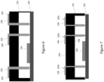
- Figures 4, 5 , and 7 illustrate further embodiments of a semiconductor package which meets a plurality of predetermined electrical, mechanical, chemical and/or environmental requirements, and which includes one or more semiconductor dies 200 covered by a molded plastic body 202.
- the molded plastic body 202 forms a housing or lid that is attached to a substrate 204.
- Each semiconductor die 200 included in the package is attached to the substrate 204 which can be, e.g., a die paddle of a leadframe, circuit board, ceramic laminate, a ceramic substrate such as a DCB (direct copper bonded), AMB (active metal brazed) or DAB (direct aluminum bonded) substrate, substrates assembled on a base plate, etc.
- a DCB direct copper bonded
- AMB active metal brazed
- DAB direct aluminum bonded
- Terminals 206 of the package are attached to the substrate 204 and protrude through the molded plastic body 202.
- the package terminals 206 are electrically connected to contact pads on each semiconductor die 200 e.g. by wire bonds, metal clips, metal ribbons, flexible boards, chip embedding technology such as eWLB (embedded wafer level ball grid array), etc. Electrical connections between the package terminals 206 and each semiconductor die 200 included in the package are not shown for ease of illustration in Figures 4 through 8 .
- Each semiconductor die 200 housed within the package may include one or more active devices, the type of which is unimportant as previously explained herein in connection with Figures 1 through 3 .
- a coating 208 is selectively applied to desired regions of the molded plastic body 202 to ensure that each predetermined electrical, mechanical, chemical and/or environmental requirement assigned to the semiconductor package and not satisfied by the molded plastic body 202 is satisfied by the coating 208.
- Selective coating can be realized by applying a mask to regions of the molded plastic body 202 not to be covered by the coating 208. The mask is removed e.g. using a solvent after the coating is applied. In another example, a blanket coating process is followed by a selective etching process which removes the coating 208 from regions of the molded plastic body 202.
- Figure 5 illustrates an embodiment of a semiconductor package which is similar to the embodiment illustrated in Figure 4 . Different, however, the sidewalls 208a, 208b of the molded plastic body 202 are also covered by the coating 208.
- the package terminals 206 are inserted into the molded plastic body 202 after the coating 208 is applied to the terminals 206.
- the coating 208 is applied to the package terminals 206 and the coated terminals 206 are then injection molded into the plastic body 202.
- transfer molding the coating 208 is applied to the package terminals 206, the coated terminals 206 are attached to the substrate 204, and afterwards the module is transfer molded. In either case, the coating 208 withstands the temperature of the molding process.
- the package terminals 206 are molded into the plastic body 202.
- the coating 208 is then applied to the entire package with the terminals 206.
- the coating 208 is removed from external contact surfaces 206a of the package terminals 206, to ensure proper connection to another body e.g. such as a circuit board.
- a mask can be applied to the external contact surfaces 206a of the package terminals 206, or the coating 208 can be removed by an etching process.
- Figure 8 illustrates an example of a semiconductor package not falling under the scope of the claims which is similar to the example illustrated in Figure 6 .
- a thicker coating 208a is applied to adjacent package terminals 206p which are at different electric potentials (e.g. source and drain potentials, collector and emitter potentials, or anode and cathode potentials) as compared to other ones of the package terminals (e.g. gate or signal terminals).
- the thicker coating 208a applied to the power terminals 206p of the package can isolate the full voltage.
- the thicker coating 208a applied to adjacent ones of the package terminals 208a at different potentials has a thickness in a range between 50 micrometres ( ⁇ m) and 1 millimetre (mm) to isolate the adjacent terminals 206p at different potentials.
- the coating 106/208 can be poly-para-xylylene, a thermoplastic or thermoset polymer, silicone or thixotropic silicone, an epoxy, polyester, etc.
- the molded plastic body 102/202 of the semiconductor package comprises a flame-retardant material and fulfils predetermined mechanical, fire, smoke and CTI>600V requirements. Corrosion or other chemical action on the package terminals 104/206 which are in physical contact with the molded plastic body 102/202 is prevented or at least minimized by a coating 106/208 applied to at least part of the molded plastic body 102/202 and/or part of the package terminals 104/206 by a CVD (chemical vapor deposition) process.
- CVD chemical vapor deposition
- para-cyclophane is used to deposit a poly-para-xylylene layer having a thickness of at least 1 ⁇ m, preferably between 1 ⁇ m and 25 ⁇ m.
- the molded plastic body 102/202 is coated completely or only in areas where the package terminals 104/206 contact the body 102/202, and also between the terminals 104/206, e.g. along creepage paths.
- the CVD coating process can be selective in that the package terminals 104/206 can be coated outside contact areas of the terminals 104/206 which make contact to other electrical conductors of the system.
- a mask can be applied to the regions of the molded plastic body 102/202 and/or package terminals 104/206 not to be covered by the coating 106/208.
- the mask is removed e.g. using a solvent after the coating 106/208 is applied.
- a blanket coating process is followed by a selective etching process which removes the coating 106/208 from regions of the molded plastic body 102/202 and/or package terminals 104/206.
- the molded plastic body 102/202 of the semiconductor package comprises a flame-retardant material and fulfils predetermined mechanical, fire, smoke and CTI>600V requirements. Corrosion or other chemical action on the package terminals 104/206 which are in physical contact with the molded plastic body 102/202 is prevented or at least minimized by a coating 106/208 applied to at least part of the molded plastic body 102/202 and/or part of the package terminals 106/208 by an electrostatic powder coating process. Clean thermoplastic or thermoset polymers are deposited during the electrostatic powder coating process. The resulting coating 106/208 can have a thickness of least 50 ⁇ m, e.g. > 100 ⁇ m.
- the electrostatic powder coating process can be selected as described above, so that the package terminals 104/206 are coated outside contact areas which make contact to other electrical conductors of the system.
- the molded plastic body 102/202 of the semiconductor package comprises a flame-retardant material and fulfils predetermined mechanical, fire, smoke and CTI>600V requirements. Leakage current through the molded plastic body 102/202 and between the package terminals 104/206 is prevented by a selective coating, accomplished by an electrostatic powder coating process.
- the coating 106/208 is a thermoplastic or thermoset polymer having a deposited thickness in a range between 50 micrometres and 1 millimetre. Such a thick coating ensures dielectric strength and takes over a significant part, if not all, of the voltage to be isolated between the package terminals 104/206.
- the molded plastic body 102/202 of the semiconductor package comprises a flame-retardant material and fulfils predetermined mechanical, fire and smoke requirements but not the CTI requirement for the package. Corrosion or other chemical action on the package terminals 104/206 which are in physical contact with the molded plastic body 102/202 is prevented or at least minimized by a coating 106/208 that comprises a plastic material which does not require additives for flame retardance and fire and smoke requirements, such as PPS (polyphenylene sulfide), LCP (liquid-crystal polymer), silicone, thixotropic silicone, etc.
- the plastic-based coating 106/208 achieves a high CTI-value e.g. >600V.
- the coating 106/208 is deposited on selective areas of the molded plastic body 102/202 and optionally on the package terminals 104/206 where high CTI is required, e.g. by an electrostatic powder coating process.
- the coating 106/208 is applied by whirl sintering which allows for thicker layers such as 0.5mm, 1mm or even thicker coatings applied to the molded plastic body 102/202 and/or the package terminals 104/206.
- coatings based on epoxy, polyester or thermoplastics can be used in both electrostatic powder coating or whirl sintering processes.
- any of the coatings described above preferably have a low content of aggressive ions, which are known to cause corrosion or change characteristics of semiconductors, directly or indirectly.
- Some examples of such ions are chlorine, sodium, potassium, fluorine, phosphorous or any other ions and ionic molecules which can be extracted by water or water vapor from the coating material.
- the maximum content of ions and/or ionic molecules which can be extracted from the coating 106/208 by water or water vapor preferably have a maximum content below 1000ppm or 100ppm by weight, according to an embodiment.
- the extractable ionic content of the coating material can be detected as follows.
- the coating material in its final form is reduced to power form for investigation (e.g. particle size ⁇ 100 ⁇ m).
- the powder is mixed with deionized water in a clean environment (e.g. clean room 10000 or better).
- a clean environment e.g. clean room 10000 or better.
- the sample is stored at a temperature of about 90 °C for about 30 minutes.
- the sample is then filtered. Ion chromatography of water with dissolved ions indicates the content of aggressive ions.
Landscapes
- Chemical & Material Sciences (AREA)
- Engineering & Computer Science (AREA)
- Materials Engineering (AREA)
- Organic Chemistry (AREA)
- Structures Or Materials For Encapsulating Or Coating Semiconductor Devices Or Solid State Devices (AREA)
Claims (10)
- Halbleitergehäuse, das mehrere vorbestimmte elektrische, mechanische, chemische und/oder ökologische Anforderungen erfüllt, wobei das Halbleitergehäuse Folgendes umfasst:einen Halbleiter-Die (100), der in einem vergossenen Kunststoffkörper (102) eingebettet oder durch diesen bedeckt ist, wobei der vergossene Kunststoffkörper (102) ein flammenhemmendes Material umfasst und nur eine Teilmenge der mehreren vorbestimmten elektrischen, mechanischen, chemischen und/oder ökologischen Anforderungen erfüllt;mehrere Anschlüsse (104), die von dem vergossenen Kunststoffkörper (102) hervorstehen und elektrisch mit dem Halbleiter-Die (100) verbunden sind; undeine Beschichtung (106), die auf den vergossenen Kunststoffkörper (102) aufgebracht ist, wobei entweder die Beschichtung (106) den vergossenen Kunststoffkörper (102) vollständig beschichtet oder die Beschichtung (106) auf den vergossenen Kunststoffkörper (102) nur in einem Gebiet aufgebracht ist, in dem die mehreren Anschlüsse (106) von dem Kunststoffkörper (102) hervorstehen, einschließlich zwischen angrenzenden der Anschlüsse (104), wobei die Beschichtung (106) ein Kunststoffmaterial umfasst und jede vorbestimmte elektrische, mechanische, chemische und/oder ökologische Anforderung erfüllt, die durch den vergossenen Kunststoffkörper nicht erfüllt wird, wobei der vergossene Kunststoffkörper (102) einen ersten Comparative-Tracking-Index(Vergleichszahl für Kriechstromfestigkeit)-Wert erzielt, der die Comparative-Tracking-Index-Anforderungen für das Halbleitergehäuse nicht erfüllt, und die Beschichtung (106) einen zweiten Comparative-Tracking-Index-Wert erzielt, der höher als der erste Comparative-Tracking-Index-Wert des vergossenen Kunststoffkörpers (102) ist und der die Comparative-Tracking-Index-Anforderungen erfüllt.
- Halbleitergehäuse nach Anspruch 1, wobei die Beschichtung (106) ferner auf die mehreren Anschlüsse (104) nur in einem Gebiet aufgebracht ist, in dem die mehreren Anschlüsse (104) von dem vergossenen Kunststoffkörper (102) hervorstehen, einschließlich zwischen angrenzenden der Anschlüsse (104), so dass eine Korrosionsbarriere zwischen den mehreren Anschlüssen (104) und dem vergossenen Kunststoffkörper (102) bereitgestellt wird.
- Halbleitergehäuse nach Anspruch 2, wobei die Beschichtung (106), die auf angrenzende der Anschlüsse (104) angewandt wird, die dazu konfiguriert sind, sich auf unterschiedlichen Potentialen zu befinden, eine Dicke in einem Bereich zwischen 50 Mikrometer und 1 Millimeter aufweist, um diejenigen angrenzenden Anschlüsse zu isolieren, die dazu konfiguriert sind, sich auf unterschiedlichen Potentialen zu befinden.
- Halbleitergehäuse nach einem der Ansprüche 1 bis 3, wobeidie Beschichtung (106) ein thermoplastisches oder duroplastisches Polymer umfasst; oderdie Beschichtung (106) Silikon oder thixotropes Silikon umfasst.
- Halbleitergehäuse nach einem der Ansprüche 1 bis 4, wobei die Beschichtung (106) insofern einen niedrigen Ionenanteil aufweist, dass Ionen und/oder ionische Moleküle, die durch Wasser oder Wasserdampf aus der Beschichtung (106) extrahiert werden können, einen maximalen Gewichtsanteil unterhalb von 1000 ppm aufweisen.
- Halbleitergehäuse nach Anspruch 5, wobei der maximale Gewichtsanteil der Ionen und/oder ionischen Moleküle der Beschichtung (106) unterhalb von 100 ppm liegt.
- Verfahren zum Herstellen eines Halbleitergehäuses, das mehrere vorbestimmte elektrische, mechanische, chemische und/oder ökologische Anforderungen erfüllt, wobei das Verfahren Folgendes umfasst:Aufbringen einer Beschichtung (106) auf den vergossenen Kunststoffkörper (102), wobei entweder die Beschichtung (106) aufgebracht wird, um den vergossenen Kunststoffkörper (102) vollständig zu beschichten, oder die Beschichtung (106) auf den vergossenen Kunststoffkörper (102) nur in einem Gebiet aufgebracht wird, in dem die mehreren Anschlüsse (106) von dem vergossenen Kunststoffkörper (102) hervorstehen, einschließlich zwischen angrenzenden der Anschlüsse (104), wobei der vergossene Kunststoffkörper (102) ein flammenhemmendes Material umfasst; undEinbetten oder Bedecken eines Halbleiter-Die (100) durch den vergossenen Kunststoffkörper (102),wobei die Anschlüsse (104) von dem vergossenen Kunststoffkörper (102) hervorstehen und elektrisch mit dem Halbleiter-Die (100) verbunden sind,wobei der vergossene Kunststoffkörper (102) nur eine Teilmenge der mehreren vorbestimmten elektrischen, mechanischen, chemischen und/oder ökologischen Anforderungen erfüllt,wobei die Beschichtung (106) ein Kunststoffmaterial umfasst und jede vorbestimmte elektrische, mechanische, chemische und/oder ökologische Anforderung erfüllt, die durch den vergossenen Kunststoffkörper nicht erfüllt wird,wobei der vergossene Kunststoffkörper (102) einen ersten Comparative-Tracking-Index-Wert erzielt, der die Comparative-Tracking-Index-Anforderungen für das Halbleitergehäuse nicht erfüllt, undwobei die Beschichtung (106) einen zweiten Comparative-Tracking-Index-Wert erzielt, der höher als der erste Comparative-Tracking-Index-Wert des vergossenen Kunststoffkörpers (102) ist und der die Comparative-Tracking-Index-Anforderungen erfüllt.
- Verfahren nach Anspruch 7, wobei das Aufbringen der Beschichtung (106) auf den vergossenen Kunststoffkörper (102) Folgendes umfasst:Abscheiden von Paracyclophan mittels eines Chemische-Gasphasenabscheidung-Prozesses auf dem gesamten vergossenen Kunststoffkörper (102) oder in einem Gebiet,in dem die mehreren Anschlüsse (106) von dem vergossenen Kunststoffkörper (102) hervorstehen, einschließlich zwischen angrenzenden der Anschlüsse (104).
- Verfahren nach Anspruch 7 oder 8, wobei das Aufbringen der Beschichtung (106) auf den vergossenen Kunststoffkörper (102) Folgendes umfasst:
Aufbringen der Beschichtung (106) auf den gesamten vergossenen Kunststoffkörper (102) oder in einem Gebiet, in dem die mehreren Anschlüsse (106) von dem vergossenen Kunststoffkörper (102) hervorstehen, einschließlich zwischen angrenzenden der Anschlüsse (104), nachdem der vergossene Kunststoffkörper (102) mit den mehreren Anschlüssen (104) gebildet wurde. - Verfahren nach einem der Ansprüche 7 bis 9, das ferner Folgendes umfasst:
Aufbringen der Beschichtung (106) auf die mehreren Anschlüsse (104) nur in einem Gebiet, in dem die mehreren Anschlüsse (104) von dem vergossenen Kunststoffkörper (102) hervorstehen, wobei die Beschichtung (106) mit einer größeren Dicke auf angrenzende Anschlüsse, die dazu konfiguriert sind, sich auf unterschiedlichen Potentialen zu befinden, als auf andere der Anschlüsse (104) aufgebracht wird.
Applications Claiming Priority (1)
| Application Number | Priority Date | Filing Date | Title |
|---|---|---|---|
| US15/380,656 US10177057B2 (en) | 2016-12-15 | 2016-12-15 | Power semiconductor modules with protective coating |
Publications (2)
| Publication Number | Publication Date |
|---|---|
| EP3336890A1 EP3336890A1 (de) | 2018-06-20 |
| EP3336890B1 true EP3336890B1 (de) | 2025-03-05 |
Family
ID=60888149
Family Applications (1)
| Application Number | Title | Priority Date | Filing Date |
|---|---|---|---|
| EP17206860.3A Active EP3336890B1 (de) | 2016-12-15 | 2017-12-13 | Leistungshalbleitermodule mit schutzbeschichtung und verfahren zu deren herstellung |
Country Status (3)
| Country | Link |
|---|---|
| US (1) | US10177057B2 (de) |
| EP (1) | EP3336890B1 (de) |
| CN (1) | CN108231705B (de) |
Families Citing this family (5)
| Publication number | Priority date | Publication date | Assignee | Title |
|---|---|---|---|---|
| DE102018219880B4 (de) * | 2018-11-20 | 2023-11-16 | Danfoss Silicon Power Gmbh | Leistungselektrikanordnung |
| CN115023805B (zh) * | 2020-02-06 | 2025-02-11 | 三菱电机株式会社 | 半导体模块和电力变换装置 |
| US20230197584A1 (en) * | 2020-05-26 | 2023-06-22 | Rohm Co., Ltd. | Mounting structure for semiconductor module |
| EP4002454A1 (de) | 2020-11-23 | 2022-05-25 | Hitachi Energy Switzerland AG | Elektrische kontaktanordnung, leistungshalbleitermodul, verfahren zur herstellung einer elektrischen kontaktanordnung und verfahren zur herstellung eines leistungshalbleitermoduls |
| CN115190704B (zh) * | 2022-07-04 | 2024-12-13 | 西安爱科赛博电气股份有限公司 | 一种电源模块的组合防护及灌封工艺方法 |
Citations (2)
| Publication number | Priority date | Publication date | Assignee | Title |
|---|---|---|---|---|
| US6046507A (en) * | 1997-12-08 | 2000-04-04 | Advanced Micro Devices | Electrophoretic coating methodology to improve internal package delamination and wire bond reliability |
| US20110309375A1 (en) * | 2010-06-16 | 2011-12-22 | Mitsubishi Electric Corporation | Semiconductor device |
Family Cites Families (43)
| Publication number | Priority date | Publication date | Assignee | Title |
|---|---|---|---|---|
| US4323914A (en) | 1979-02-01 | 1982-04-06 | International Business Machines Corporation | Heat transfer structure for integrated circuit package |
| US5164816A (en) | 1988-12-29 | 1992-11-17 | Hitachi Chemical Co., Ltd. | Integrated circuit device produced with a resin layer produced from a heat-resistant resin paste |
| US5274913A (en) | 1991-10-25 | 1994-01-04 | International Business Machines Corporation | Method of fabricating a reworkable module |
| US5268202A (en) | 1992-10-09 | 1993-12-07 | Rensselaer Polytechnic Institute | Vapor deposition of parylene-F using 1,4-bis (trifluoromethyl) benzene |
| US5656830A (en) | 1992-12-10 | 1997-08-12 | International Business Machines Corp. | Integrated circuit chip composite having a parylene coating |
| US5825042A (en) * | 1993-06-18 | 1998-10-20 | Space Electronics, Inc. | Radiation shielding of plastic integrated circuits |
| US5405808A (en) | 1993-08-16 | 1995-04-11 | Lsi Logic Corporation | Fluid-filled and gas-filled semiconductor packages |
| US6140144A (en) | 1996-08-08 | 2000-10-31 | Integrated Sensing Systems, Inc. | Method for packaging microsensors |
| US6885522B1 (en) | 1999-05-28 | 2005-04-26 | Fujitsu Limited | Head assembly having integrated circuit chip covered by layer which prevents foreign particle generation |
| US6368899B1 (en) * | 2000-03-08 | 2002-04-09 | Maxwell Electronic Components Group, Inc. | Electronic device packaging |
| US6956283B1 (en) | 2000-05-16 | 2005-10-18 | Peterson Kenneth A | Encapsulants for protecting MEMS devices during post-packaging release etch |
| JP2002158328A (ja) | 2000-11-17 | 2002-05-31 | Mitsubishi Electric Corp | 電力用半導体装置 |
| DE10130517C2 (de) | 2001-06-25 | 2003-07-24 | Eupec Gmbh & Co Kg | Hochspannungsmodul und Verfahren zu dessen Herstellung |
| DE10149886A1 (de) | 2001-10-10 | 2003-04-30 | Eupec Gmbh & Co Kg | Leistunghalbleitermodul |
| FR2833802B1 (fr) | 2001-12-13 | 2004-03-12 | Valeo Electronique | Module de puissance et ensemble de modules de puissance |
| US6770822B2 (en) | 2002-02-22 | 2004-08-03 | Bridgewave Communications, Inc. | High frequency device packages and methods |
| US7517790B2 (en) | 2002-10-31 | 2009-04-14 | International Business Machines Corporation | Method and structure to enhance temperature/humidity/bias performance of semiconductor devices by surface modification |
| US7116557B1 (en) | 2003-05-23 | 2006-10-03 | Sti Electronics, Inc. | Imbedded component integrated circuit assembly and method of making same |
| TWI255832B (en) * | 2003-06-11 | 2006-06-01 | Ind Tech Res Inst | Method of reducing the photoelectric device current leakage in conjugated polymer and conjugated polymer composition |
| JP4081611B2 (ja) | 2003-11-19 | 2008-04-30 | 株式会社豊田自動織機 | 半導体装置 |
| WO2005061576A1 (ja) * | 2003-12-19 | 2005-07-07 | Daisankasei Co., Ltd. | ポリパラキシリレンおよびその誘導体膜の熱安定性向上方法ならびにポリパラキシリレン誘導体 |
| US20070262426A1 (en) * | 2004-01-27 | 2007-11-15 | Joachim Mahler | Semiconductor Housings Having Coupling Coatings |
| JP2005332874A (ja) | 2004-05-18 | 2005-12-02 | Hitachi Metals Ltd | 回路基板及びこれを用いた半導体装置 |
| JP2006179856A (ja) | 2004-11-25 | 2006-07-06 | Fuji Electric Holdings Co Ltd | 絶縁基板および半導体装置 |
| EP1905079A2 (de) | 2005-07-07 | 2008-04-02 | Koninklijke Philips Electronics N.V. | Verpackung, herstellungsverfahren dafür und anwendung davon |
| JP4884830B2 (ja) | 2006-05-11 | 2012-02-29 | 三菱電機株式会社 | 半導体装置 |
| US7767589B2 (en) | 2007-02-07 | 2010-08-03 | Raytheon Company | Passivation layer for a circuit device and method of manufacture |
| US9214442B2 (en) | 2007-03-19 | 2015-12-15 | Infineon Technologies Ag | Power semiconductor module, method for producing a power semiconductor module, and semiconductor chip |
| JP2009016383A (ja) * | 2007-06-29 | 2009-01-22 | Fujitsu Ltd | パッケージドデバイスおよびパッケージドデバイス製造方法 |
| US8674462B2 (en) | 2007-07-25 | 2014-03-18 | Infineon Technologies Ag | Sensor package |
| US8154114B2 (en) | 2007-08-06 | 2012-04-10 | Infineon Technologies Ag | Power semiconductor module |
| US7944033B2 (en) | 2007-10-18 | 2011-05-17 | Infineon Technologies Ag | Power semiconductor module |
| US8581113B2 (en) | 2007-12-19 | 2013-11-12 | Bridgewave Communications, Inc. | Low cost high frequency device package and methods |
| US20100164083A1 (en) * | 2008-12-29 | 2010-07-01 | Numonyx B.V. | Protective thin film coating in chip packaging |
| US8525340B2 (en) | 2010-06-11 | 2013-09-03 | Premitec, Inc. | Flexible electronic devices and related methods |
| US8933548B2 (en) * | 2010-11-02 | 2015-01-13 | Dai Nippon Printing Co., Ltd. | Lead frame for mounting LED elements, lead frame with resin, method for manufacturing semiconductor devices, and lead frame for mounting semiconductor elements |
| US8766436B2 (en) | 2011-03-01 | 2014-07-01 | Lsi Corporation | Moisture barrier for a wire bond |
| US8847412B2 (en) | 2012-11-09 | 2014-09-30 | Invensas Corporation | Microelectronic assembly with thermally and electrically conductive underfill |
| US20150001700A1 (en) | 2013-06-28 | 2015-01-01 | Infineon Technologies Ag | Power Modules with Parylene Coating |
| TWM498961U (zh) | 2013-07-03 | 2015-04-11 | 羅森伯格高頻技術公司 | 高頻寬互連線的熱絕緣結構 |
| JP6127837B2 (ja) | 2013-08-30 | 2017-05-17 | 株式会社デンソー | 半導体装置 |
| DE102014112406A1 (de) * | 2014-08-28 | 2016-03-03 | Infineon Technologies Ag | Einbettung additiver Partikel in einer Verkapselung einer elektronischen Vorrichtung |
| CN105977309B (zh) * | 2016-07-23 | 2019-11-08 | 中国振华集团永光电子有限公司(国营第八七三厂) | 一种高可靠抗辐照玻璃钝化快恢复整流二极管制造方法 |
-
2016
- 2016-12-15 US US15/380,656 patent/US10177057B2/en active Active
-
2017
- 2017-12-13 EP EP17206860.3A patent/EP3336890B1/de active Active
- 2017-12-15 CN CN201711349402.2A patent/CN108231705B/zh active Active
Patent Citations (2)
| Publication number | Priority date | Publication date | Assignee | Title |
|---|---|---|---|---|
| US6046507A (en) * | 1997-12-08 | 2000-04-04 | Advanced Micro Devices | Electrophoretic coating methodology to improve internal package delamination and wire bond reliability |
| US20110309375A1 (en) * | 2010-06-16 | 2011-12-22 | Mitsubishi Electric Corporation | Semiconductor device |
Also Published As
| Publication number | Publication date |
|---|---|
| US20180174936A1 (en) | 2018-06-21 |
| CN108231705A (zh) | 2018-06-29 |
| CN108231705B (zh) | 2021-06-22 |
| EP3336890A1 (de) | 2018-06-20 |
| US10177057B2 (en) | 2019-01-08 |
Similar Documents
| Publication | Publication Date | Title |
|---|---|---|
| EP3336890B1 (de) | Leistungshalbleitermodule mit schutzbeschichtung und verfahren zu deren herstellung | |
| US12401000B2 (en) | Semiconductor device | |
| CN107535050B (zh) | 多层总线板 | |
| US11848213B2 (en) | Semiconductor module having a layer that includes inorganic filler and a casting material | |
| US9572291B2 (en) | Semiconductor device and method for manufacturing same | |
| US6873049B2 (en) | Near hermetic power chip on board device and manufacturing method therefor | |
| EP2074653B1 (de) | Grossflächiger Leistungshalbleiter in Kunststoffpackung für Oberflächenmontage | |
| JPS6220700B2 (de) | ||
| US10483179B2 (en) | Semiconductor device with sealing portion to suppress connection corrosion | |
| JP7158392B2 (ja) | パワー半導体モジュール | |
| CN118943094B (zh) | 半导体封装结构 | |
| CN101111144B (zh) | 热导管 | |
| CN116981918A (zh) | 隔离式温度传感器器件封装件 | |
| EP3477694B1 (de) | Leistungshalbleitermodul mit teilbeschichteten leistungsanschlüssen | |
| US11417591B2 (en) | Semiconductor module | |
| US10424528B2 (en) | Layered cooling structure including insulative layer and multiple metallization layers | |
| CN118451792A (zh) | 具有增强的保护的堆叠式多芯片结构 | |
| CN116457938A (zh) | 半导体模块 | |
| EP4345889A1 (de) | Verfahren zur verbesserung der paketkriechstrecke | |
| EP4459675A1 (de) | Verfahren zur verbesserung der paketkriechstrecke | |
| US20230282601A1 (en) | Semiconductor joining, semiconductor device | |
| US20250285924A1 (en) | Semiconductor device | |
| US20190131039A1 (en) | Positive temperature coefficient devices with oxygen barrier packages | |
| CN113937064A (zh) | 半导体电路 | |
| HK40107301A (zh) | 具有增强的保护的堆叠式多芯片结构 |
Legal Events
| Date | Code | Title | Description |
|---|---|---|---|
| PUAI | Public reference made under article 153(3) epc to a published international application that has entered the european phase |
Free format text: ORIGINAL CODE: 0009012 |
|
| STAA | Information on the status of an ep patent application or granted ep patent |
Free format text: STATUS: THE APPLICATION HAS BEEN PUBLISHED |
|
| AK | Designated contracting states |
Kind code of ref document: A1 Designated state(s): AL AT BE BG CH CY CZ DE DK EE ES FI FR GB GR HR HU IE IS IT LI LT LU LV MC MK MT NL NO PL PT RO RS SE SI SK SM TR |
|
| AX | Request for extension of the european patent |
Extension state: BA ME |
|
| STAA | Information on the status of an ep patent application or granted ep patent |
Free format text: STATUS: REQUEST FOR EXAMINATION WAS MADE |
|
| 17P | Request for examination filed |
Effective date: 20181219 |
|
| RBV | Designated contracting states (corrected) |
Designated state(s): AL AT BE BG CH CY CZ DE DK EE ES FI FR GB GR HR HU IE IS IT LI LT LU LV MC MK MT NL NO PL PT RO RS SE SI SK SM TR |
|
| STAA | Information on the status of an ep patent application or granted ep patent |
Free format text: STATUS: EXAMINATION IS IN PROGRESS |
|
| 17Q | First examination report despatched |
Effective date: 20200907 |
|
| GRAP | Despatch of communication of intention to grant a patent |
Free format text: ORIGINAL CODE: EPIDOSNIGR1 |
|
| STAA | Information on the status of an ep patent application or granted ep patent |
Free format text: STATUS: GRANT OF PATENT IS INTENDED |
|
| RIC1 | Information provided on ipc code assigned before grant |
Ipc: C09K 21/06 20060101ALI20241107BHEP Ipc: H01L 23/29 20060101ALI20241107BHEP Ipc: H01L 23/31 20060101AFI20241107BHEP |
|
| RIC1 | Information provided on ipc code assigned before grant |
Ipc: C09K 21/06 20060101ALI20241114BHEP Ipc: H01L 23/31 20060101AFI20241114BHEP |
|
| INTG | Intention to grant announced |
Effective date: 20241128 |
|
| GRAS | Grant fee paid |
Free format text: ORIGINAL CODE: EPIDOSNIGR3 |
|
| GRAA | (expected) grant |
Free format text: ORIGINAL CODE: 0009210 |
|
| STAA | Information on the status of an ep patent application or granted ep patent |
Free format text: STATUS: THE PATENT HAS BEEN GRANTED |
|
| P01 | Opt-out of the competence of the unified patent court (upc) registered |
Free format text: CASE NUMBER: APP_1160/2025 Effective date: 20250108 |
|
| AK | Designated contracting states |
Kind code of ref document: B1 Designated state(s): AL AT BE BG CH CY CZ DE DK EE ES FI FR GB GR HR HU IE IS IT LI LT LU LV MC MK MT NL NO PL PT RO RS SE SI SK SM TR |
|
| REG | Reference to a national code |
Ref country code: GB Ref legal event code: FG4D |
|
| REG | Reference to a national code |
Ref country code: CH Ref legal event code: EP |
|
| REG | Reference to a national code |
Ref country code: DE Ref legal event code: R096 Ref document number: 602017088140 Country of ref document: DE |
|
| REG | Reference to a national code |
Ref country code: IE Ref legal event code: FG4D |
|
| PG25 | Lapsed in a contracting state [announced via postgrant information from national office to epo] |
Ref country code: RS Free format text: LAPSE BECAUSE OF FAILURE TO SUBMIT A TRANSLATION OF THE DESCRIPTION OR TO PAY THE FEE WITHIN THE PRESCRIBED TIME-LIMIT Effective date: 20250605 |
|
| PG25 | Lapsed in a contracting state [announced via postgrant information from national office to epo] |
Ref country code: FI Free format text: LAPSE BECAUSE OF FAILURE TO SUBMIT A TRANSLATION OF THE DESCRIPTION OR TO PAY THE FEE WITHIN THE PRESCRIBED TIME-LIMIT Effective date: 20250305 |
|
| REG | Reference to a national code |
Ref country code: NL Ref legal event code: MP Effective date: 20250305 |
|
| PG25 | Lapsed in a contracting state [announced via postgrant information from national office to epo] |
Ref country code: ES Free format text: LAPSE BECAUSE OF FAILURE TO SUBMIT A TRANSLATION OF THE DESCRIPTION OR TO PAY THE FEE WITHIN THE PRESCRIBED TIME-LIMIT Effective date: 20250305 |
|
| REG | Reference to a national code |
Ref country code: LT Ref legal event code: MG9D |
|
| PG25 | Lapsed in a contracting state [announced via postgrant information from national office to epo] |
Ref country code: NO Free format text: LAPSE BECAUSE OF FAILURE TO SUBMIT A TRANSLATION OF THE DESCRIPTION OR TO PAY THE FEE WITHIN THE PRESCRIBED TIME-LIMIT Effective date: 20250605 |
|
| PG25 | Lapsed in a contracting state [announced via postgrant information from national office to epo] |
Ref country code: HR Free format text: LAPSE BECAUSE OF FAILURE TO SUBMIT A TRANSLATION OF THE DESCRIPTION OR TO PAY THE FEE WITHIN THE PRESCRIBED TIME-LIMIT Effective date: 20250305 |
|
| PG25 | Lapsed in a contracting state [announced via postgrant information from national office to epo] |
Ref country code: LV Free format text: LAPSE BECAUSE OF FAILURE TO SUBMIT A TRANSLATION OF THE DESCRIPTION OR TO PAY THE FEE WITHIN THE PRESCRIBED TIME-LIMIT Effective date: 20250305 |
|
| PG25 | Lapsed in a contracting state [announced via postgrant information from national office to epo] |
Ref country code: GR Free format text: LAPSE BECAUSE OF FAILURE TO SUBMIT A TRANSLATION OF THE DESCRIPTION OR TO PAY THE FEE WITHIN THE PRESCRIBED TIME-LIMIT Effective date: 20250606 Ref country code: BG Free format text: LAPSE BECAUSE OF FAILURE TO SUBMIT A TRANSLATION OF THE DESCRIPTION OR TO PAY THE FEE WITHIN THE PRESCRIBED TIME-LIMIT Effective date: 20250305 |
|
| REG | Reference to a national code |
Ref country code: AT Ref legal event code: MK05 Ref document number: 1773767 Country of ref document: AT Kind code of ref document: T Effective date: 20250305 |
|
| PG25 | Lapsed in a contracting state [announced via postgrant information from national office to epo] |
Ref country code: NL Free format text: LAPSE BECAUSE OF FAILURE TO SUBMIT A TRANSLATION OF THE DESCRIPTION OR TO PAY THE FEE WITHIN THE PRESCRIBED TIME-LIMIT Effective date: 20250305 |
|
| PG25 | Lapsed in a contracting state [announced via postgrant information from national office to epo] |
Ref country code: SE Free format text: LAPSE BECAUSE OF FAILURE TO SUBMIT A TRANSLATION OF THE DESCRIPTION OR TO PAY THE FEE WITHIN THE PRESCRIBED TIME-LIMIT Effective date: 20250305 |
|
| PG25 | Lapsed in a contracting state [announced via postgrant information from national office to epo] |
Ref country code: SM Free format text: LAPSE BECAUSE OF FAILURE TO SUBMIT A TRANSLATION OF THE DESCRIPTION OR TO PAY THE FEE WITHIN THE PRESCRIBED TIME-LIMIT Effective date: 20250305 |
|
| PG25 | Lapsed in a contracting state [announced via postgrant information from national office to epo] |
Ref country code: PT Free format text: LAPSE BECAUSE OF FAILURE TO SUBMIT A TRANSLATION OF THE DESCRIPTION OR TO PAY THE FEE WITHIN THE PRESCRIBED TIME-LIMIT Effective date: 20250707 |
|
| PG25 | Lapsed in a contracting state [announced via postgrant information from national office to epo] |
Ref country code: PL Free format text: LAPSE BECAUSE OF FAILURE TO SUBMIT A TRANSLATION OF THE DESCRIPTION OR TO PAY THE FEE WITHIN THE PRESCRIBED TIME-LIMIT Effective date: 20250305 Ref country code: IT Free format text: LAPSE BECAUSE OF FAILURE TO SUBMIT A TRANSLATION OF THE DESCRIPTION OR TO PAY THE FEE WITHIN THE PRESCRIBED TIME-LIMIT Effective date: 20250305 |
|
| PG25 | Lapsed in a contracting state [announced via postgrant information from national office to epo] |
Ref country code: AT Free format text: LAPSE BECAUSE OF FAILURE TO SUBMIT A TRANSLATION OF THE DESCRIPTION OR TO PAY THE FEE WITHIN THE PRESCRIBED TIME-LIMIT Effective date: 20250305 |
|
| PG25 | Lapsed in a contracting state [announced via postgrant information from national office to epo] |
Ref country code: CZ Free format text: LAPSE BECAUSE OF FAILURE TO SUBMIT A TRANSLATION OF THE DESCRIPTION OR TO PAY THE FEE WITHIN THE PRESCRIBED TIME-LIMIT Effective date: 20250305 Ref country code: EE Free format text: LAPSE BECAUSE OF FAILURE TO SUBMIT A TRANSLATION OF THE DESCRIPTION OR TO PAY THE FEE WITHIN THE PRESCRIBED TIME-LIMIT Effective date: 20250305 |
|
| PG25 | Lapsed in a contracting state [announced via postgrant information from national office to epo] |
Ref country code: RO Free format text: LAPSE BECAUSE OF FAILURE TO SUBMIT A TRANSLATION OF THE DESCRIPTION OR TO PAY THE FEE WITHIN THE PRESCRIBED TIME-LIMIT Effective date: 20250305 |
|
| PG25 | Lapsed in a contracting state [announced via postgrant information from national office to epo] |
Ref country code: SK Free format text: LAPSE BECAUSE OF FAILURE TO SUBMIT A TRANSLATION OF THE DESCRIPTION OR TO PAY THE FEE WITHIN THE PRESCRIBED TIME-LIMIT Effective date: 20250305 |
|
| PG25 | Lapsed in a contracting state [announced via postgrant information from national office to epo] |
Ref country code: IS Free format text: LAPSE BECAUSE OF FAILURE TO SUBMIT A TRANSLATION OF THE DESCRIPTION OR TO PAY THE FEE WITHIN THE PRESCRIBED TIME-LIMIT Effective date: 20250705 |
|
| REG | Reference to a national code |
Ref country code: DE Ref legal event code: R079 Ref document number: 602017088140 Country of ref document: DE Free format text: PREVIOUS MAIN CLASS: H01L0023310000 Ipc: H10W0074100000 |
|
| REG | Reference to a national code |
Ref country code: DE Ref legal event code: R097 Ref document number: 602017088140 Country of ref document: DE |
|
| PLBE | No opposition filed within time limit |
Free format text: ORIGINAL CODE: 0009261 |
|
| STAA | Information on the status of an ep patent application or granted ep patent |
Free format text: STATUS: NO OPPOSITION FILED WITHIN TIME LIMIT |
|
| PG25 | Lapsed in a contracting state [announced via postgrant information from national office to epo] |
Ref country code: DK Free format text: LAPSE BECAUSE OF FAILURE TO SUBMIT A TRANSLATION OF THE DESCRIPTION OR TO PAY THE FEE WITHIN THE PRESCRIBED TIME-LIMIT Effective date: 20250305 |
|
| REG | Reference to a national code |
Ref country code: CH Ref legal event code: L10 Free format text: ST27 STATUS EVENT CODE: U-0-0-L10-L00 (AS PROVIDED BY THE NATIONAL OFFICE) Effective date: 20260114 |
|
| 26N | No opposition filed |
Effective date: 20251208 |
|
| PGFP | Annual fee paid to national office [announced via postgrant information from national office to epo] |
Ref country code: DE Payment date: 20260224 Year of fee payment: 9 |