EP4459675A1 - Verfahren zur verbesserung der paketkriechstrecke - Google Patents
Verfahren zur verbesserung der paketkriechstrecke Download PDFInfo
- Publication number
- EP4459675A1 EP4459675A1 EP23171465.0A EP23171465A EP4459675A1 EP 4459675 A1 EP4459675 A1 EP 4459675A1 EP 23171465 A EP23171465 A EP 23171465A EP 4459675 A1 EP4459675 A1 EP 4459675A1
- Authority
- EP
- European Patent Office
- Prior art keywords
- package
- creepage
- insulating material
- coating
- semiconductor package
- Prior art date
- Legal status (The legal status is an assumption and is not a legal conclusion. Google has not performed a legal analysis and makes no representation as to the accuracy of the status listed.)
- Pending
Links
Images
Classifications
-
- H—ELECTRICITY
- H10—SEMICONDUCTOR DEVICES; ELECTRIC SOLID-STATE DEVICES NOT OTHERWISE PROVIDED FOR
- H10W—GENERIC PACKAGES, INTERCONNECTIONS, CONNECTORS OR OTHER CONSTRUCTIONAL DETAILS OF DEVICES COVERED BY CLASS H10
- H10W74/00—Encapsulations, e.g. protective coatings
- H10W74/01—Manufacture or treatment
-
- H—ELECTRICITY
- H10—SEMICONDUCTOR DEVICES; ELECTRIC SOLID-STATE DEVICES NOT OTHERWISE PROVIDED FOR
- H10W—GENERIC PACKAGES, INTERCONNECTIONS, CONNECTORS OR OTHER CONSTRUCTIONAL DETAILS OF DEVICES COVERED BY CLASS H10
- H10W70/00—Package substrates; Interposers; Redistribution layers [RDL]
- H10W70/40—Leadframes
- H10W70/481—Leadframes for devices being provided for in groups H10D8/00 - H10D48/00
-
- H—ELECTRICITY
- H10—SEMICONDUCTOR DEVICES; ELECTRIC SOLID-STATE DEVICES NOT OTHERWISE PROVIDED FOR
- H10W—GENERIC PACKAGES, INTERCONNECTIONS, CONNECTORS OR OTHER CONSTRUCTIONAL DETAILS OF DEVICES COVERED BY CLASS H10
- H10W70/00—Package substrates; Interposers; Redistribution layers [RDL]
- H10W70/60—Insulating or insulated package substrates; Interposers; Redistribution layers
- H10W70/67—Insulating or insulated package substrates; Interposers; Redistribution layers characterised by their insulating layers or insulating parts
- H10W70/68—Shapes or dispositions thereof
- H10W70/6875—Shapes or dispositions thereof being on a metallic substrate, e.g. insulated metal substrates [IMS]
-
- H—ELECTRICITY
- H10—SEMICONDUCTOR DEVICES; ELECTRIC SOLID-STATE DEVICES NOT OTHERWISE PROVIDED FOR
- H10W—GENERIC PACKAGES, INTERCONNECTIONS, CONNECTORS OR OTHER CONSTRUCTIONAL DETAILS OF DEVICES COVERED BY CLASS H10
- H10W40/00—Arrangements for thermal protection or thermal control
- H10W40/20—Arrangements for cooling
- H10W40/25—Arrangements for cooling characterised by their materials
-
- H—ELECTRICITY
- H10—SEMICONDUCTOR DEVICES; ELECTRIC SOLID-STATE DEVICES NOT OTHERWISE PROVIDED FOR
- H10W—GENERIC PACKAGES, INTERCONNECTIONS, CONNECTORS OR OTHER CONSTRUCTIONAL DETAILS OF DEVICES COVERED BY CLASS H10
- H10W70/00—Package substrates; Interposers; Redistribution layers [RDL]
- H10W70/40—Leadframes
- H10W70/421—Shapes or dispositions
- H10W70/424—Cross-sectional shapes
- H10W70/427—Bent parts
- H10W70/429—Bent parts being the outer leads
-
- H—ELECTRICITY
- H10—SEMICONDUCTOR DEVICES; ELECTRIC SOLID-STATE DEVICES NOT OTHERWISE PROVIDED FOR
- H10W—GENERIC PACKAGES, INTERCONNECTIONS, CONNECTORS OR OTHER CONSTRUCTIONAL DETAILS OF DEVICES COVERED BY CLASS H10
- H10W70/00—Package substrates; Interposers; Redistribution layers [RDL]
- H10W70/40—Leadframes
- H10W70/456—Materials
- H10W70/458—Materials of insulating layers on leadframes
-
- H—ELECTRICITY
- H10—SEMICONDUCTOR DEVICES; ELECTRIC SOLID-STATE DEVICES NOT OTHERWISE PROVIDED FOR
- H10W—GENERIC PACKAGES, INTERCONNECTIONS, CONNECTORS OR OTHER CONSTRUCTIONAL DETAILS OF DEVICES COVERED BY CLASS H10
- H10W74/00—Encapsulations, e.g. protective coatings
- H10W74/10—Encapsulations, e.g. protective coatings characterised by their shape or disposition
- H10W74/111—Encapsulations, e.g. protective coatings characterised by their shape or disposition the semiconductor body being completely enclosed
-
- H—ELECTRICITY
- H10—SEMICONDUCTOR DEVICES; ELECTRIC SOLID-STATE DEVICES NOT OTHERWISE PROVIDED FOR
- H10W—GENERIC PACKAGES, INTERCONNECTIONS, CONNECTORS OR OTHER CONSTRUCTIONAL DETAILS OF DEVICES COVERED BY CLASS H10
- H10W74/00—Encapsulations, e.g. protective coatings
- H10W74/10—Encapsulations, e.g. protective coatings characterised by their shape or disposition
- H10W74/111—Encapsulations, e.g. protective coatings characterised by their shape or disposition the semiconductor body being completely enclosed
- H10W74/121—Encapsulations, e.g. protective coatings characterised by their shape or disposition the semiconductor body being completely enclosed by multiple encapsulations, e.g. by a thin protective coating and a thick encapsulation
-
- H—ELECTRICITY
- H10—SEMICONDUCTOR DEVICES; ELECTRIC SOLID-STATE DEVICES NOT OTHERWISE PROVIDED FOR
- H10W—GENERIC PACKAGES, INTERCONNECTIONS, CONNECTORS OR OTHER CONSTRUCTIONAL DETAILS OF DEVICES COVERED BY CLASS H10
- H10W74/00—Encapsulations, e.g. protective coatings
- H10W74/40—Encapsulations, e.g. protective coatings characterised by their materials
Definitions
- the present disclosure is directed to a method improving package creepage distance for an integrated circuit package, in particular for high voltage devices.
- Creepage and clearance are typical industry standard critical properties for packages of discrete semiconductors and Integrated Circuits, ICs.
- Clearance may be defined as the shortest distance in air between two conductors. Hence, as the shortest distance is through air, it can be understood as, or comparable to the line of sight between to peaks, i.e. given no obstacles between two conductors, it is the shortest distance between the conductors.
- Creepage is closely related to clearance however and may be defined as the shortest distance between two conductors along the surface of the insulating material. Hence, in comparison with the example of clearance, instead of the shortest distance over air, the shortest distance over land between the two peaks.
- creepage and also clearance are very important, and with the trend in increase in voltages of the devices, which may even exceed 500V, and trend of miniaturization of semiconductor device packages, creepage and clearance becomes even more important.
- Insufficient creepage may result in voltage breakdown in which the voltage between two conductors overcomes the insulation in between the conductors and may create an arc or conductive path across the surface of the insulating material which can damage the device, cause failure of the operation of the device and may cause hazardous situations.
- Creepage properties can be improved by increasing the distance between the two conductors. Typically, that will increase the package size, which is contrary to the desire for miniaturization.
- creepage properties may be improved by adding plastics over exposed conductive parts of the package. This however requires additional measure to be taken in the assembling of the end user device.
- Yet another alternative to improve creepage properties is the use of leadframes package designs, which however result in reduction of heatsink size, which in turn has decreases thermal properties of the package.
- a method of improving semiconductor package creepage wherein the package comprises a semiconductor device, and a plurality of electrically conductive contacts at a surface of the package, the package comprising insulating material for electrically insulating the package between the plurality of electrically conductive contacts, wherein an initial creepage distance is defined by the shortest distance over the surface of the package between two of the plurality of contacts, and the method comprising the steps of: - applying a coating over at least part of said insulating material of said package, wherein said coating has an electrical volume resistivity higher than an electrical volume resistivity of said insulating material of said package to increase the initial creepage distance and improve package creepage of the semiconductor package.
- Safety and reliability are two important measures in the design and use of semiconductor devices, especially for high voltage applications. In general these measures may relate to the packages which house the semiconductor devices, and to the Printed Circuit Boards, PCB, on which the semiconductor packages or devices are mounted (e.g. soldered).
- Creepage and clearance are two typical properties for both the PCB and the packages which have a high impact on the reliability and the safety. As such, certain applications, environments and/or designed maximum operating voltage levels may require certain levels of creepage and clearance.
- Certain commonly used semiconductor packages have standard pin-to-pin clearance and creepage distances. Newer versions of the same package standard may further increase pin-to-pin clearance to improve safety and reliability and/or to set higher maximum voltage levels.
- the packages for such applications have two or three leads and a metal tab like surface which may allow mounting to an external heatsink and functions as a heatsink to allow the device to dissipate heat.
- Improving creepage distance by modification of such packages may have an impact on the heat dissipation capabilities of the device, which especially for high voltage packages and thus high power applications may be a problem.
- CTI comparative tracking index
- CTI may be considered a standard, used to measure the resistance of a material to surface tracking caused by electrical leakage. Surface tracking occurs when a conductive path is formed on the surface of a material, which can cause a short circuit or electrical breakdown.
- the CTI value may be determined by exposing a sample of the material to a high voltage (typically 600 volts) and tracking the number of seconds it takes for a conductive path to form on the surface of the material. The time taken for the conductive path to form is compared to that of other materials tested under the same conditions.
- the higher the CTI value the more resistant the material is to surface tracking.
- the CTI is expressed in units of volts and is a measure of the voltage level at which a material will track when compared to other materials. The higher the CTI value, the higher the voltage that can be applied to the material before it starts to track.
- the CTI value is important in selecting materials for electrical and electronic applications, particularly in determining the safety and reliability of electrical insulation materials. A higher CTI value indicates that the material is less likely to cause electrical problems, and is therefore more suitable for use in high-voltage applications.
- Non-organic insulators as glass or ceramics have the property that they will not track and thus have a high CTI value, as no conductive paths under high voltage conditions will be formed.
- What is proposed, is to apply a coating of the insulating material of the package, i.e. the plastic surface of the semiconductor package, with a thin layer of inorganic coating material to overcome the tracking issue.
- a coating of the insulating material of the package i.e. the plastic surface of the semiconductor package
- the coating thus is categorized preferably in material group I or II, more preferably in group I, having a CTI index of at least 400, more preferably at least 500, even more preferably at least 600 VAC, or most preferably, a unlimited CTI index such as glass or ceramics, or any other suitable inorganic coating material which can be applied in semiconductor packaging processes and which do not breakdown on the surface.
- the electrical volume resistivity of said coating is in the range of 1 x 10 16 to 1 x 10 18 ⁇ -cm, more preferably in the range of 5 x 10 16 to 5 x 10 17 ⁇ -cm and most preferably in the range of 8 x 10 16 to 2 x 10 17 ⁇ -cm.
- the coating has an increased thermal resistance of a factor 3 or less, and more preferably a factor 2 or less, as compared to said electrically conductive contacts of said package.
- the coating comprises a layer of insulating material selected from one of the group of: Al2O3/TiO2, parylene, polyimide or other polymer materials as used for conformal coating of PCBs in electronic equipment.
- the coating comprises a layer of insulating material is applied with a thickness of less than 100 ⁇ m, more preferably less than 10 ⁇ m, most preferably less than 1 ⁇ m.
- the coating comprises a layer of insulating material which is applied by Atomic Layer Deposition, ALD.
- the coating comprises a layer of insulating material which is applied by a deposition method, preferably a vacuum deposition method, and more preferably a chemical vapor deposition method.
- the coating comprises a layer of insulating material which is applied by sputtering.
- the coating comprises a layer of insulating material which is applied by spraying.
- the coating comprises a layer of insulating material which is further applied to a part of at least one of said plurality of electrically conductive contacts of said package.
- the coating comprises a layer of insulating material which is further applied to all of said plurality of electrically conductive contacts of said package.
- the coating comprises a layer of insulating material which is applied over all of said insulating material of said package.
- the coating comprises a layer of insulating material which is further applied to a heatsink of said package.
- the device is a discrete Surface-Mounted Device, SMD, semiconductor device or a discrete Thin High Phosphorus, THP, semiconductor device.
- a semiconductor package having a coating applied over at least part of said insulating material of said package, wherein said coating has an electrical volume resistivity higher than an electrical volume resistivity of said insulating material of said package to increase the initial creepage distance and improve package creepage of the semiconductor package, and wherein the application of said coating is performed in accordance with the first aspect of the present disclosure.
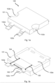
- Fig. 1a and 1b disclose a typical semiconductor package 100 comprising discrete semiconductor components or Integrated Circuit(s), IC(s).
- the semiconductor package 100 comprises the semiconductor device, and a plurality of electrically conductive contacts 102a, 102b, 102c, 102d, 102e at a surface of the package. These contacts are conductive and exposed, as can been seen in Fig. 1a and 1b .
- the package 100 shown here by way of example has two leadframes or leadframe strips, or simply leads 102a, 102b.
- the example shown in Fig. 1a, 1b also has two notches 102c, 102d, which are used for molding the package and a heatsink 102e or contact surface for fixing the package 100 onto an external heatsink (not shown).
- the semiconductor package further comprises insulating material 101 for electrically insulating the package 100 between the plurality of electrically conductive contacts 102a-e.
- Creepage is a typical industry standard critical property for packages of discrete semiconductors and Integrated Circuits, ICs. Creepage may be defined as the shortest distance between two conductors along the surface of the insulating material. When looking at Fig. 1b , there are two types of creepage, the creepage distance on the PCB 104, which may also be defined as the clearance as the shortest distance through air between two electrically conductive surfaces of the package, and creepage distance on the package 105, which is the shortest distance over the surface of the package between two electrically conductive surfaces of the package.
- the proposed method to improve creepage properties may improve one but preferably both of the creepage distance on the PCB 104 and the creepage distance on the package 105.
- the creepage 104, 105, 106 prior to the method according to the present disclosure is defined as the initial creepage distance.
- the initial creepage distance which is thus the shortest distance between two of a plurality of contacts of the package, in the example shown in Fig 1b , the distance 104 between 102a and 102e, and/or the distance 105 between 102b and 102e and the distance 106 between 102a and 102b.
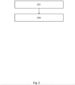
- Fig. 2 discloses the basic steps 201, 202 of a method of improving semiconductor package creepage.
- the semiconductor package comprises a semiconductor device, and a plurality of electrically conductive contacts at a surface of the package.
- the semiconductor package further comprises insulating material for electrically insulating the package between the plurality of electrically conductive contacts.
- a semiconductor package is provided.
- the semiconductor package comprises discrete semiconductors and/or integrated circuits.
- the initial creepage distance is defined by the shortest distance over the surface of the package between two of the plurality of contacts.
- the package comprises a plurality of electrically conductive contacts at a surface of the package, and comprises insulating material for electrically insulating the package between the plurality of electrically conductive contacts.
- the package without performing the method according to the present disclosure, has an initial creepage distance.
- a coating is applied over at least part of said insulating material of said semiconductor package.
- the package has electrical contacts, being the heatsink 102e of the package, the leadframe strips 102a, 102b, dam bar area, or any other exposed conductive, e.g. metal, parts of the package such as the mould notches 102c, 102d.
- the coating is thus applied to at least one of the insulating areas or also referred to as the package or plastic areas of the package, and may preferably also be applied to the exposed conductive areas of the package.
- the coating may cover part or all of the exposed area of the plastic and preferably part or all of the conductive areas.
- the coating has an electrical volume resistivity higher than an electrical volume resistivity of the insulating material, hence the plastic of the package. This way the initial creepage is improved and thereby the package creepage of the semiconductor package is improved as well. This is even further improved when also part or all of the exposed conductive areas is covered by the coating.
- the coating is applied in accordance with step 202 in a thin layer, e.g. less than 100 ⁇ m, more preferably less than 10 ⁇ m, most preferably less than 1 ⁇ m, and may comprise one or more of Al2O3/TiO2, parylene, polyimide or other polymer materials as used for conformal coating of PCBs in electronic equipment.
- any layer of insulating material over the package and preferably over exposed electrically conducting area, either fully covering the area or partly covering it, will lower electrical conductivity, however, the coating is applied in such a way, that the thermal conductivity, due to the layer thickness, is decreased to a lesser degree than the degree in electrical conductivity.
- This can be achieved through application of various materials in a thin layer, and to such an extent that a package thermal resistance increase is less than a factor 3, or preferably to a factor 2, when compared to an uncoated semiconductor package. Accordingly, the initial creepage is increased and the overall package creepage of the semiconductor package is improved.
- the package creepage is improved, and only when the conductive areas are coated as well, the thermal resistance is increased to a limited extent, e.g. with a maximum of a factor 3 or 2 of the initial thermal resistance of the package, such a package on the one hand meets minimum creepage distance of electrical conductors as described e.g., in IEC60664-1 and IPC2221A, whereas on the other hand, the thermal resistance is still within prescribed range to meet packaging requirements.
- the thermal path for the package for cooling is electrically isolated, to such a degree that the creepage properties are improved but with minimal, and at least within specification, reduction in thermal conductivity.
- the coating may be applied in full, or partially, on part of the package and preferably on one of the exposed electrical contacts, or on several or all of the electrical contacts such as on the heatsink.
- the coating can be applied in addition or alternatively also at the leads (e.g., at area of dambar remains) close to package or on top of the exposed metal parts of mould notch.
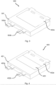
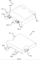
- Fig. 3 4 , 5 and 6 four different examples 300, 400, 500, 600 are shown of a package on which the method of the present disclosure is applied.
- plastic area of the package are according to the present disclosure partially or fully coated by a material like an ALD layer, parylene or other insulating coating materials like conformal coating materials.
- the coating material has a CTI value according to material group 1 (refer IEC60664-1) to minimize the required distances of metal parts of the package.
- ALD coating materials like Al2O3/TiO2 will not track at all.
- the coating material as applied to metal parts of plastic body of the packages comprise a material such as Al2O3/TiO2 applied by ALD (atomic layer deposition), parylene, polyimide or other polymer materials as used for conformal coating of PCBs in electronic equipment.
- ALD atomic layer deposition
- parylene polyethylene
- polyimide polyimide
- Fig. 4 shown another example of a partial coating 403 of the heatsink 403e of a SMD package 401 to increase the creepage distance of the leads.
- the way of processing and coating position in the assembly flow will be as described under b).
- the assembly process of the semiconductor package will be done in usual way including moulding of the leadframe strips. Individual packages have been built and will still be on leadframe strips. Prior to galvanic tin plating the plastic bodies of the packages will be coated with one of the above-mentioned materials. Coverage of the parts of packages and metal parts (e.g., heatsink and leads) at which the coating should be not applied needs to be done prior to coating process. Alternatively, the coating can be done without masking and the coating can be removed on metal parts by electrolytic deflash as used to remove mould compound residues on metal parts after moulding. Alternatively, laser or light ablation could be used to remove the coating on metal parts.
- electrolytic deflash as used to remove mould compound residues on metal parts after moulding.
- laser or light ablation could be used to remove the coating on metal parts.
- Fig. 4 another example 400 is shown of coating a package 401, in which a full coverage 403 of the plastic package is applied.
- the way of processing and coating position in the assembly flow is already described in view of Fig. 3 .
- Keeping areas of heatsink free from coating can be done as well as described in relation to the example of Fig. 3 .
- the advantage of this method is to increase the creepage distance towards other metal conductors (e.g., package leads) after soldering on PCB in customer application.
- Fig. 5 shows yet another example of additionally coating the leads and preferably part of plastic body at which the leads enter the plastic body (e.g., at dam bar area) to increase the creepage distance between the leads.
- the way of processing and the assembly flow can be done as described in reference to Fig. 3 , but coating is preferably done after leadframe dam bar cut. Keeping areas of metal parts (leads and heatsink) free from coating can be done as described in reference to Fig. 3 . For this option the area of leads close to plastic body will be coated.
- This problem can be solved by the embodiment shown in Fig. 5 . Due to punching operation for removing the dam bars there will be always some remains which reduce the clearance from lead to lead. The coating will isolate the dam bar remains and air to air clearance distance of uninsulated metal parts is not applicable anymore.
- Fig. 6 shows yet another example of additionally coating 603 of the exposed metal parts of mould lock or mould notch features 102c, 102d, to avoid exposed metal parts with high voltage potential.
- This embodiment solves that exposed metal parts at the package at which some mould tool feature press down the die pad to bottom mould to avoid plastic resin coverage on the heatsink (exposed Cu parts on back heatsink/packages). At this location the Cu of the die pad will remain exposed and is connected to electrical potential. Coating of the metal parts at this area will be used to isolate these areas and will help to increase creepage distances in final application.
- ALD may be used to apply Al2O3/TiO2 or parylene in very thin layers.
- the coating layer can be in sub ⁇ m thickness. This minimizes the impact of the thermal conductivity from package heatsink to external heatsink by maintaining electrical isolation.
- partially coverage of package metal parts is possible by the proposed method. No modification on package design, materials or processing is necessary.
- the proposed method allows to select mould compounds with optimal properties for e.g., adhesion (zero delamination) and best thermo-mechanical performance with more freedom on creepage related properties (material class), without requiring additional steps after manufacturing.
- conformal coating of complete assembled PCB can be skipped. As such, a flexible increase of high voltage creepage distances of semiconductor plastic packages may be achieved by partial or full conformal coating of metal parts.
- the proposed method may be applied on a large variety of packages and for various applications, amongst which:
Landscapes
- Structures Or Materials For Encapsulating Or Coating Semiconductor Devices Or Solid State Devices (AREA)
Priority Applications (3)
| Application Number | Priority Date | Filing Date | Title |
|---|---|---|---|
| EP23171465.0A EP4459675A1 (de) | 2023-05-04 | 2023-05-04 | Verfahren zur verbesserung der paketkriechstrecke |
| US18/652,878 US20240371712A1 (en) | 2023-05-04 | 2024-05-02 | Method of improving package creepage distance |
| CN202410545417.XA CN118899230A (zh) | 2023-05-04 | 2024-05-06 | 改善封装爬电距离的方法 |
Applications Claiming Priority (1)
| Application Number | Priority Date | Filing Date | Title |
|---|---|---|---|
| EP23171465.0A EP4459675A1 (de) | 2023-05-04 | 2023-05-04 | Verfahren zur verbesserung der paketkriechstrecke |
Publications (1)
| Publication Number | Publication Date |
|---|---|
| EP4459675A1 true EP4459675A1 (de) | 2024-11-06 |
Family
ID=86329121
Family Applications (1)
| Application Number | Title | Priority Date | Filing Date |
|---|---|---|---|
| EP23171465.0A Pending EP4459675A1 (de) | 2023-05-04 | 2023-05-04 | Verfahren zur verbesserung der paketkriechstrecke |
Country Status (3)
| Country | Link |
|---|---|
| US (1) | US20240371712A1 (de) |
| EP (1) | EP4459675A1 (de) |
| CN (1) | CN118899230A (de) |
Citations (4)
| Publication number | Priority date | Publication date | Assignee | Title |
|---|---|---|---|---|
| DE10142472A1 (de) * | 2001-08-31 | 2002-10-31 | Infineon Technologies Ag | Elektronisches Hochleistung- und Leistungsbauteil mit Ausgangskontaktstiften |
| US20140264944A1 (en) * | 2013-03-14 | 2014-09-18 | Infineon Technologies Austria Ag | Semiconductor Package with Top-Side Insulation Layer |
| US20210327777A1 (en) * | 2018-09-06 | 2021-10-21 | Mitsubishi Electric Corporation | Power semiconductor device and method of manufacturing the same, and power conversion device |
| US20220028765A1 (en) * | 2020-07-22 | 2022-01-27 | Texas Instruments Incorporated | Coated semiconductor devices |
-
2023
- 2023-05-04 EP EP23171465.0A patent/EP4459675A1/de active Pending
-
2024
- 2024-05-02 US US18/652,878 patent/US20240371712A1/en active Pending
- 2024-05-06 CN CN202410545417.XA patent/CN118899230A/zh active Pending
Patent Citations (4)
| Publication number | Priority date | Publication date | Assignee | Title |
|---|---|---|---|---|
| DE10142472A1 (de) * | 2001-08-31 | 2002-10-31 | Infineon Technologies Ag | Elektronisches Hochleistung- und Leistungsbauteil mit Ausgangskontaktstiften |
| US20140264944A1 (en) * | 2013-03-14 | 2014-09-18 | Infineon Technologies Austria Ag | Semiconductor Package with Top-Side Insulation Layer |
| US20210327777A1 (en) * | 2018-09-06 | 2021-10-21 | Mitsubishi Electric Corporation | Power semiconductor device and method of manufacturing the same, and power conversion device |
| US20220028765A1 (en) * | 2020-07-22 | 2022-01-27 | Texas Instruments Incorporated | Coated semiconductor devices |
Also Published As
| Publication number | Publication date |
|---|---|
| CN118899230A (zh) | 2024-11-05 |
| US20240371712A1 (en) | 2024-11-07 |
Similar Documents
| Publication | Publication Date | Title |
|---|---|---|
| US4554229A (en) | Multilayer hybrid integrated circuit | |
| US5073521A (en) | Method for housing a tape-bonded electronic device and the package employed | |
| US7193329B2 (en) | Semiconductor device | |
| EP1909321B1 (de) | Metall-keramik-verbundsubstrat und verfahren zu seiner herstellung | |
| EP1160861B1 (de) | Verfahren zur Herstellung eines thermisch leitenden Substrats mit Leiterrahmen und Wärmestrahlungsplatte | |
| EP2074653B1 (de) | Grossflächiger Leistungshalbleiter in Kunststoffpackung für Oberflächenmontage | |
| US9142430B2 (en) | High-voltage packaged device | |
| PL205553B1 (pl) | Sposób obudowania przyrządu półprzewodnikowego | |
| EP3336890B1 (de) | Leistungshalbleitermodule mit schutzbeschichtung und verfahren zu deren herstellung | |
| US20060248716A1 (en) | Self-supporting contacting structures that are directly produced on components without housings | |
| US7309838B2 (en) | Multi-layered circuit board assembly with improved thermal dissipation | |
| EP4459675A1 (de) | Verfahren zur verbesserung der paketkriechstrecke | |
| CN105895536A (zh) | 电子元件的封装方法 | |
| US20150084089A1 (en) | Insulation structure for high temperature conditions and manufacturing method thereof | |
| US5969412A (en) | Tape-fixed leadframe | |
| EP4345889A1 (de) | Verfahren zur verbesserung der paketkriechstrecke | |
| US4601972A (en) | Photodefinable triazine based composition | |
| US10424528B2 (en) | Layered cooling structure including insulative layer and multiple metallization layers | |
| WO2022223199A1 (en) | Semiconductor power module and method for manufacturing a semiconductor power module | |
| CN107278017A (zh) | 基板单元以及基板单元的制造方法 | |
| US20260123456A1 (en) | Electronic device with lead insulation | |
| EP4614560A1 (de) | Komponentenmontageplatte, verfahren zur herstellung einer komponentenmontageplatte, elektronisches modul und verfahren zur herstellung eines elektronischen moduls | |
| US20240297116A1 (en) | Integrated packaging device and fabrication methods thereof | |
| CN117727713A (zh) | 封装芯片、封装芯片制备方法及功率器件 | |
| CN102468193A (zh) | 封装装置及电子设备 |
Legal Events
| Date | Code | Title | Description |
|---|---|---|---|
| PUAI | Public reference made under article 153(3) epc to a published international application that has entered the european phase |
Free format text: ORIGINAL CODE: 0009012 |
|
| STAA | Information on the status of an ep patent application or granted ep patent |
Free format text: STATUS: THE APPLICATION HAS BEEN PUBLISHED |
|
| AK | Designated contracting states |
Kind code of ref document: A1 Designated state(s): AL AT BE BG CH CY CZ DE DK EE ES FI FR GB GR HR HU IE IS IT LI LT LU LV MC ME MK MT NL NO PL PT RO RS SE SI SK SM TR |
|
| STAA | Information on the status of an ep patent application or granted ep patent |
Free format text: STATUS: REQUEST FOR EXAMINATION WAS MADE |
|
| 17P | Request for examination filed |
Effective date: 20250506 |