EP3326182B1 - Dielektrische zusammensetzung, dielektrisches element, elektronische komponente und laminierte elektronische komponente - Google Patents
Dielektrische zusammensetzung, dielektrisches element, elektronische komponente und laminierte elektronische komponente Download PDFInfo
- Publication number
- EP3326182B1 EP3326182B1 EP16729573.2A EP16729573A EP3326182B1 EP 3326182 B1 EP3326182 B1 EP 3326182B1 EP 16729573 A EP16729573 A EP 16729573A EP 3326182 B1 EP3326182 B1 EP 3326182B1
- Authority
- EP
- European Patent Office
- Prior art keywords
- dielectric
- dielectric composition
- internal electrode
- phase
- laminated ceramic
- Prior art date
- Legal status (The legal status is an assumption and is not a legal conclusion. Google has not performed a legal analysis and makes no representation as to the accuracy of the status listed.)
- Not-in-force
Links
Images


Classifications
-
- H—ELECTRICITY
- H01—ELECTRIC ELEMENTS
- H01G—CAPACITORS; CAPACITORS, RECTIFIERS, DETECTORS, SWITCHING DEVICES, LIGHT-SENSITIVE OR TEMPERATURE-SENSITIVE DEVICES OF THE ELECTROLYTIC TYPE
- H01G4/00—Fixed capacitors; Processes of their manufacture
- H01G4/002—Details
- H01G4/018—Dielectrics
- H01G4/06—Solid dielectrics
- H01G4/08—Inorganic dielectrics
- H01G4/12—Ceramic dielectrics
- H01G4/1209—Ceramic dielectrics characterised by the ceramic dielectric material
- H01G4/1218—Ceramic dielectrics characterised by the ceramic dielectric material based on titanium oxides or titanates
- H01G4/1227—Ceramic dielectrics characterised by the ceramic dielectric material based on titanium oxides or titanates based on alkaline earth titanates
-
- C—CHEMISTRY; METALLURGY
- C04—CEMENTS; CONCRETE; ARTIFICIAL STONE; CERAMICS; REFRACTORIES
- C04B—LIME, MAGNESIA; SLAG; CEMENTS; COMPOSITIONS THEREOF, e.g. MORTARS, CONCRETE OR LIKE BUILDING MATERIALS; ARTIFICIAL STONE; CERAMICS; REFRACTORIES; TREATMENT OF NATURAL STONE
- C04B35/00—Shaped ceramic products characterised by their composition; Ceramics compositions; Processing powders of inorganic compounds preparatory to the manufacturing of ceramic products
- C04B35/01—Shaped ceramic products characterised by their composition; Ceramics compositions; Processing powders of inorganic compounds preparatory to the manufacturing of ceramic products based on oxide ceramics
- C04B35/46—Shaped ceramic products characterised by their composition; Ceramics compositions; Processing powders of inorganic compounds preparatory to the manufacturing of ceramic products based on oxide ceramics based on titanium oxides or titanates
- C04B35/462—Shaped ceramic products characterised by their composition; Ceramics compositions; Processing powders of inorganic compounds preparatory to the manufacturing of ceramic products based on oxide ceramics based on titanium oxides or titanates based on titanates
- C04B35/465—Shaped ceramic products characterised by their composition; Ceramics compositions; Processing powders of inorganic compounds preparatory to the manufacturing of ceramic products based on oxide ceramics based on titanium oxides or titanates based on titanates based on alkaline earth metal titanates
- C04B35/47—Shaped ceramic products characterised by their composition; Ceramics compositions; Processing powders of inorganic compounds preparatory to the manufacturing of ceramic products based on oxide ceramics based on titanium oxides or titanates based on titanates based on alkaline earth metal titanates based on strontium titanates
-
- C—CHEMISTRY; METALLURGY
- C04—CEMENTS; CONCRETE; ARTIFICIAL STONE; CERAMICS; REFRACTORIES
- C04B—LIME, MAGNESIA; SLAG; CEMENTS; COMPOSITIONS THEREOF, e.g. MORTARS, CONCRETE OR LIKE BUILDING MATERIALS; ARTIFICIAL STONE; CERAMICS; REFRACTORIES; TREATMENT OF NATURAL STONE
- C04B35/00—Shaped ceramic products characterised by their composition; Ceramics compositions; Processing powders of inorganic compounds preparatory to the manufacturing of ceramic products
- C04B35/01—Shaped ceramic products characterised by their composition; Ceramics compositions; Processing powders of inorganic compounds preparatory to the manufacturing of ceramic products based on oxide ceramics
- C04B35/46—Shaped ceramic products characterised by their composition; Ceramics compositions; Processing powders of inorganic compounds preparatory to the manufacturing of ceramic products based on oxide ceramics based on titanium oxides or titanates
- C04B35/462—Shaped ceramic products characterised by their composition; Ceramics compositions; Processing powders of inorganic compounds preparatory to the manufacturing of ceramic products based on oxide ceramics based on titanium oxides or titanates based on titanates
- C04B35/475—Shaped ceramic products characterised by their composition; Ceramics compositions; Processing powders of inorganic compounds preparatory to the manufacturing of ceramic products based on oxide ceramics based on titanium oxides or titanates based on titanates based on bismuth titanates
-
- C—CHEMISTRY; METALLURGY
- C04—CEMENTS; CONCRETE; ARTIFICIAL STONE; CERAMICS; REFRACTORIES
- C04B—LIME, MAGNESIA; SLAG; CEMENTS; COMPOSITIONS THEREOF, e.g. MORTARS, CONCRETE OR LIKE BUILDING MATERIALS; ARTIFICIAL STONE; CERAMICS; REFRACTORIES; TREATMENT OF NATURAL STONE
- C04B35/00—Shaped ceramic products characterised by their composition; Ceramics compositions; Processing powders of inorganic compounds preparatory to the manufacturing of ceramic products
- C04B35/622—Forming processes; Processing powders of inorganic compounds preparatory to the manufacturing of ceramic products
- C04B35/626—Preparing or treating the powders individually or as batches ; preparing or treating macroscopic reinforcing agents for ceramic products, e.g. fibres; mechanical aspects section B
- C04B35/62605—Treating the starting powders individually or as mixtures
- C04B35/6261—Milling
-
- C—CHEMISTRY; METALLURGY
- C04—CEMENTS; CONCRETE; ARTIFICIAL STONE; CERAMICS; REFRACTORIES
- C04B—LIME, MAGNESIA; SLAG; CEMENTS; COMPOSITIONS THEREOF, e.g. MORTARS, CONCRETE OR LIKE BUILDING MATERIALS; ARTIFICIAL STONE; CERAMICS; REFRACTORIES; TREATMENT OF NATURAL STONE
- C04B35/00—Shaped ceramic products characterised by their composition; Ceramics compositions; Processing powders of inorganic compounds preparatory to the manufacturing of ceramic products
- C04B35/622—Forming processes; Processing powders of inorganic compounds preparatory to the manufacturing of ceramic products
- C04B35/626—Preparing or treating the powders individually or as batches ; preparing or treating macroscopic reinforcing agents for ceramic products, e.g. fibres; mechanical aspects section B
- C04B35/62605—Treating the starting powders individually or as mixtures
- C04B35/62645—Thermal treatment of powders or mixtures thereof other than sintering
-
- C—CHEMISTRY; METALLURGY
- C04—CEMENTS; CONCRETE; ARTIFICIAL STONE; CERAMICS; REFRACTORIES
- C04B—LIME, MAGNESIA; SLAG; CEMENTS; COMPOSITIONS THEREOF, e.g. MORTARS, CONCRETE OR LIKE BUILDING MATERIALS; ARTIFICIAL STONE; CERAMICS; REFRACTORIES; TREATMENT OF NATURAL STONE
- C04B35/00—Shaped ceramic products characterised by their composition; Ceramics compositions; Processing powders of inorganic compounds preparatory to the manufacturing of ceramic products
- C04B35/622—Forming processes; Processing powders of inorganic compounds preparatory to the manufacturing of ceramic products
- C04B35/626—Preparing or treating the powders individually or as batches ; preparing or treating macroscopic reinforcing agents for ceramic products, e.g. fibres; mechanical aspects section B
- C04B35/628—Coating the powders or the macroscopic reinforcing agents
- C04B35/62802—Powder coating materials
- C04B35/62805—Oxide ceramics
- C04B35/62818—Refractory metal oxides
- C04B35/62821—Titanium oxide
-
- C—CHEMISTRY; METALLURGY
- C04—CEMENTS; CONCRETE; ARTIFICIAL STONE; CERAMICS; REFRACTORIES
- C04B—LIME, MAGNESIA; SLAG; CEMENTS; COMPOSITIONS THEREOF, e.g. MORTARS, CONCRETE OR LIKE BUILDING MATERIALS; ARTIFICIAL STONE; CERAMICS; REFRACTORIES; TREATMENT OF NATURAL STONE
- C04B35/00—Shaped ceramic products characterised by their composition; Ceramics compositions; Processing powders of inorganic compounds preparatory to the manufacturing of ceramic products
- C04B35/622—Forming processes; Processing powders of inorganic compounds preparatory to the manufacturing of ceramic products
- C04B35/64—Burning or sintering processes
-
- C—CHEMISTRY; METALLURGY
- C04—CEMENTS; CONCRETE; ARTIFICIAL STONE; CERAMICS; REFRACTORIES
- C04B—LIME, MAGNESIA; SLAG; CEMENTS; COMPOSITIONS THEREOF, e.g. MORTARS, CONCRETE OR LIKE BUILDING MATERIALS; ARTIFICIAL STONE; CERAMICS; REFRACTORIES; TREATMENT OF NATURAL STONE
- C04B41/00—After-treatment of mortars, concrete, artificial stone or ceramics; Treatment of natural stone
- C04B41/45—Coating or impregnating, e.g. injection in masonry, partial coating of green or fired ceramics, organic coating compositions for adhering together two concrete elements
- C04B41/4578—Coating or impregnating of green ceramics or unset concrete
-
- C—CHEMISTRY; METALLURGY
- C04—CEMENTS; CONCRETE; ARTIFICIAL STONE; CERAMICS; REFRACTORIES
- C04B—LIME, MAGNESIA; SLAG; CEMENTS; COMPOSITIONS THEREOF, e.g. MORTARS, CONCRETE OR LIKE BUILDING MATERIALS; ARTIFICIAL STONE; CERAMICS; REFRACTORIES; TREATMENT OF NATURAL STONE
- C04B41/00—After-treatment of mortars, concrete, artificial stone or ceramics; Treatment of natural stone
- C04B41/45—Coating or impregnating, e.g. injection in masonry, partial coating of green or fired ceramics, organic coating compositions for adhering together two concrete elements
- C04B41/50—Coating or impregnating, e.g. injection in masonry, partial coating of green or fired ceramics, organic coating compositions for adhering together two concrete elements with inorganic materials
- C04B41/51—Metallising, e.g. infiltration of sintered ceramic preforms with molten metal
- C04B41/5111—Ag, Au, Pd, Pt or Cu
-
- C—CHEMISTRY; METALLURGY
- C04—CEMENTS; CONCRETE; ARTIFICIAL STONE; CERAMICS; REFRACTORIES
- C04B—LIME, MAGNESIA; SLAG; CEMENTS; COMPOSITIONS THEREOF, e.g. MORTARS, CONCRETE OR LIKE BUILDING MATERIALS; ARTIFICIAL STONE; CERAMICS; REFRACTORIES; TREATMENT OF NATURAL STONE
- C04B41/00—After-treatment of mortars, concrete, artificial stone or ceramics; Treatment of natural stone
- C04B41/80—After-treatment of mortars, concrete, artificial stone or ceramics; Treatment of natural stone of only ceramics
- C04B41/81—Coating or impregnation
- C04B41/85—Coating or impregnation with inorganic materials
- C04B41/88—Metals
-
- H—ELECTRICITY
- H01—ELECTRIC ELEMENTS
- H01G—CAPACITORS; CAPACITORS, RECTIFIERS, DETECTORS, SWITCHING DEVICES, LIGHT-SENSITIVE OR TEMPERATURE-SENSITIVE DEVICES OF THE ELECTROLYTIC TYPE
- H01G4/00—Fixed capacitors; Processes of their manufacture
- H01G4/002—Details
- H01G4/005—Electrodes
- H01G4/012—Form of non-self-supporting electrodes
-
- H—ELECTRICITY
- H01—ELECTRIC ELEMENTS
- H01G—CAPACITORS; CAPACITORS, RECTIFIERS, DETECTORS, SWITCHING DEVICES, LIGHT-SENSITIVE OR TEMPERATURE-SENSITIVE DEVICES OF THE ELECTROLYTIC TYPE
- H01G4/00—Fixed capacitors; Processes of their manufacture
- H01G4/002—Details
- H01G4/018—Dielectrics
- H01G4/06—Solid dielectrics
- H01G4/08—Inorganic dielectrics
- H01G4/12—Ceramic dielectrics
- H01G4/1209—Ceramic dielectrics characterised by the ceramic dielectric material
- H01G4/1218—Ceramic dielectrics characterised by the ceramic dielectric material based on titanium oxides or titanates
-
- H—ELECTRICITY
- H01—ELECTRIC ELEMENTS
- H01G—CAPACITORS; CAPACITORS, RECTIFIERS, DETECTORS, SWITCHING DEVICES, LIGHT-SENSITIVE OR TEMPERATURE-SENSITIVE DEVICES OF THE ELECTROLYTIC TYPE
- H01G4/00—Fixed capacitors; Processes of their manufacture
- H01G4/30—Stacked capacitors
-
- C—CHEMISTRY; METALLURGY
- C04—CEMENTS; CONCRETE; ARTIFICIAL STONE; CERAMICS; REFRACTORIES
- C04B—LIME, MAGNESIA; SLAG; CEMENTS; COMPOSITIONS THEREOF, e.g. MORTARS, CONCRETE OR LIKE BUILDING MATERIALS; ARTIFICIAL STONE; CERAMICS; REFRACTORIES; TREATMENT OF NATURAL STONE
- C04B2235/00—Aspects relating to ceramic starting mixtures or sintered ceramic products
- C04B2235/02—Composition of constituents of the starting material or of secondary phases of the final product
- C04B2235/30—Constituents and secondary phases not being of a fibrous nature
- C04B2235/32—Metal oxides, mixed metal oxides, or oxide-forming salts thereof, e.g. carbonates, nitrates, (oxy)hydroxides, chlorides
- C04B2235/3201—Alkali metal oxides or oxide-forming salts thereof
- C04B2235/3203—Lithium oxide or oxide-forming salts thereof
-
- C—CHEMISTRY; METALLURGY
- C04—CEMENTS; CONCRETE; ARTIFICIAL STONE; CERAMICS; REFRACTORIES
- C04B—LIME, MAGNESIA; SLAG; CEMENTS; COMPOSITIONS THEREOF, e.g. MORTARS, CONCRETE OR LIKE BUILDING MATERIALS; ARTIFICIAL STONE; CERAMICS; REFRACTORIES; TREATMENT OF NATURAL STONE
- C04B2235/00—Aspects relating to ceramic starting mixtures or sintered ceramic products
- C04B2235/02—Composition of constituents of the starting material or of secondary phases of the final product
- C04B2235/30—Constituents and secondary phases not being of a fibrous nature
- C04B2235/32—Metal oxides, mixed metal oxides, or oxide-forming salts thereof, e.g. carbonates, nitrates, (oxy)hydroxides, chlorides
- C04B2235/3205—Alkaline earth oxides or oxide forming salts thereof, e.g. beryllium oxide
- C04B2235/3206—Magnesium oxides or oxide-forming salts thereof
-
- C—CHEMISTRY; METALLURGY
- C04—CEMENTS; CONCRETE; ARTIFICIAL STONE; CERAMICS; REFRACTORIES
- C04B—LIME, MAGNESIA; SLAG; CEMENTS; COMPOSITIONS THEREOF, e.g. MORTARS, CONCRETE OR LIKE BUILDING MATERIALS; ARTIFICIAL STONE; CERAMICS; REFRACTORIES; TREATMENT OF NATURAL STONE
- C04B2235/00—Aspects relating to ceramic starting mixtures or sintered ceramic products
- C04B2235/02—Composition of constituents of the starting material or of secondary phases of the final product
- C04B2235/30—Constituents and secondary phases not being of a fibrous nature
- C04B2235/32—Metal oxides, mixed metal oxides, or oxide-forming salts thereof, e.g. carbonates, nitrates, (oxy)hydroxides, chlorides
- C04B2235/3205—Alkaline earth oxides or oxide forming salts thereof, e.g. beryllium oxide
- C04B2235/3208—Calcium oxide or oxide-forming salts thereof, e.g. lime
-
- C—CHEMISTRY; METALLURGY
- C04—CEMENTS; CONCRETE; ARTIFICIAL STONE; CERAMICS; REFRACTORIES
- C04B—LIME, MAGNESIA; SLAG; CEMENTS; COMPOSITIONS THEREOF, e.g. MORTARS, CONCRETE OR LIKE BUILDING MATERIALS; ARTIFICIAL STONE; CERAMICS; REFRACTORIES; TREATMENT OF NATURAL STONE
- C04B2235/00—Aspects relating to ceramic starting mixtures or sintered ceramic products
- C04B2235/02—Composition of constituents of the starting material or of secondary phases of the final product
- C04B2235/30—Constituents and secondary phases not being of a fibrous nature
- C04B2235/32—Metal oxides, mixed metal oxides, or oxide-forming salts thereof, e.g. carbonates, nitrates, (oxy)hydroxides, chlorides
- C04B2235/3205—Alkaline earth oxides or oxide forming salts thereof, e.g. beryllium oxide
- C04B2235/3213—Strontium oxides or oxide-forming salts thereof
-
- C—CHEMISTRY; METALLURGY
- C04—CEMENTS; CONCRETE; ARTIFICIAL STONE; CERAMICS; REFRACTORIES
- C04B—LIME, MAGNESIA; SLAG; CEMENTS; COMPOSITIONS THEREOF, e.g. MORTARS, CONCRETE OR LIKE BUILDING MATERIALS; ARTIFICIAL STONE; CERAMICS; REFRACTORIES; TREATMENT OF NATURAL STONE
- C04B2235/00—Aspects relating to ceramic starting mixtures or sintered ceramic products
- C04B2235/02—Composition of constituents of the starting material or of secondary phases of the final product
- C04B2235/30—Constituents and secondary phases not being of a fibrous nature
- C04B2235/32—Metal oxides, mixed metal oxides, or oxide-forming salts thereof, e.g. carbonates, nitrates, (oxy)hydroxides, chlorides
- C04B2235/3205—Alkaline earth oxides or oxide forming salts thereof, e.g. beryllium oxide
- C04B2235/3215—Barium oxides or oxide-forming salts thereof
-
- C—CHEMISTRY; METALLURGY
- C04—CEMENTS; CONCRETE; ARTIFICIAL STONE; CERAMICS; REFRACTORIES
- C04B—LIME, MAGNESIA; SLAG; CEMENTS; COMPOSITIONS THEREOF, e.g. MORTARS, CONCRETE OR LIKE BUILDING MATERIALS; ARTIFICIAL STONE; CERAMICS; REFRACTORIES; TREATMENT OF NATURAL STONE
- C04B2235/00—Aspects relating to ceramic starting mixtures or sintered ceramic products
- C04B2235/02—Composition of constituents of the starting material or of secondary phases of the final product
- C04B2235/30—Constituents and secondary phases not being of a fibrous nature
- C04B2235/32—Metal oxides, mixed metal oxides, or oxide-forming salts thereof, e.g. carbonates, nitrates, (oxy)hydroxides, chlorides
- C04B2235/3224—Rare earth oxide or oxide forming salts thereof, e.g. scandium oxide
- C04B2235/3227—Lanthanum oxide or oxide-forming salts thereof
-
- C—CHEMISTRY; METALLURGY
- C04—CEMENTS; CONCRETE; ARTIFICIAL STONE; CERAMICS; REFRACTORIES
- C04B—LIME, MAGNESIA; SLAG; CEMENTS; COMPOSITIONS THEREOF, e.g. MORTARS, CONCRETE OR LIKE BUILDING MATERIALS; ARTIFICIAL STONE; CERAMICS; REFRACTORIES; TREATMENT OF NATURAL STONE
- C04B2235/00—Aspects relating to ceramic starting mixtures or sintered ceramic products
- C04B2235/02—Composition of constituents of the starting material or of secondary phases of the final product
- C04B2235/30—Constituents and secondary phases not being of a fibrous nature
- C04B2235/32—Metal oxides, mixed metal oxides, or oxide-forming salts thereof, e.g. carbonates, nitrates, (oxy)hydroxides, chlorides
- C04B2235/3224—Rare earth oxide or oxide forming salts thereof, e.g. scandium oxide
- C04B2235/3229—Cerium oxides or oxide-forming salts thereof
-
- C—CHEMISTRY; METALLURGY
- C04—CEMENTS; CONCRETE; ARTIFICIAL STONE; CERAMICS; REFRACTORIES
- C04B—LIME, MAGNESIA; SLAG; CEMENTS; COMPOSITIONS THEREOF, e.g. MORTARS, CONCRETE OR LIKE BUILDING MATERIALS; ARTIFICIAL STONE; CERAMICS; REFRACTORIES; TREATMENT OF NATURAL STONE
- C04B2235/00—Aspects relating to ceramic starting mixtures or sintered ceramic products
- C04B2235/02—Composition of constituents of the starting material or of secondary phases of the final product
- C04B2235/30—Constituents and secondary phases not being of a fibrous nature
- C04B2235/32—Metal oxides, mixed metal oxides, or oxide-forming salts thereof, e.g. carbonates, nitrates, (oxy)hydroxides, chlorides
- C04B2235/3231—Refractory metal oxides, their mixed metal oxides, or oxide-forming salts thereof
- C04B2235/3232—Titanium oxides or titanates, e.g. rutile or anatase
- C04B2235/3234—Titanates, not containing zirconia
- C04B2235/3236—Alkaline earth titanates
-
- C—CHEMISTRY; METALLURGY
- C04—CEMENTS; CONCRETE; ARTIFICIAL STONE; CERAMICS; REFRACTORIES
- C04B—LIME, MAGNESIA; SLAG; CEMENTS; COMPOSITIONS THEREOF, e.g. MORTARS, CONCRETE OR LIKE BUILDING MATERIALS; ARTIFICIAL STONE; CERAMICS; REFRACTORIES; TREATMENT OF NATURAL STONE
- C04B2235/00—Aspects relating to ceramic starting mixtures or sintered ceramic products
- C04B2235/02—Composition of constituents of the starting material or of secondary phases of the final product
- C04B2235/30—Constituents and secondary phases not being of a fibrous nature
- C04B2235/32—Metal oxides, mixed metal oxides, or oxide-forming salts thereof, e.g. carbonates, nitrates, (oxy)hydroxides, chlorides
- C04B2235/3284—Zinc oxides, zincates, cadmium oxides, cadmiates, mercury oxides, mercurates or oxide forming salts thereof
-
- C—CHEMISTRY; METALLURGY
- C04—CEMENTS; CONCRETE; ARTIFICIAL STONE; CERAMICS; REFRACTORIES
- C04B—LIME, MAGNESIA; SLAG; CEMENTS; COMPOSITIONS THEREOF, e.g. MORTARS, CONCRETE OR LIKE BUILDING MATERIALS; ARTIFICIAL STONE; CERAMICS; REFRACTORIES; TREATMENT OF NATURAL STONE
- C04B2235/00—Aspects relating to ceramic starting mixtures or sintered ceramic products
- C04B2235/02—Composition of constituents of the starting material or of secondary phases of the final product
- C04B2235/30—Constituents and secondary phases not being of a fibrous nature
- C04B2235/32—Metal oxides, mixed metal oxides, or oxide-forming salts thereof, e.g. carbonates, nitrates, (oxy)hydroxides, chlorides
- C04B2235/3298—Bismuth oxides, bismuthates or oxide forming salts thereof, e.g. zinc bismuthate
-
- C—CHEMISTRY; METALLURGY
- C04—CEMENTS; CONCRETE; ARTIFICIAL STONE; CERAMICS; REFRACTORIES
- C04B—LIME, MAGNESIA; SLAG; CEMENTS; COMPOSITIONS THEREOF, e.g. MORTARS, CONCRETE OR LIKE BUILDING MATERIALS; ARTIFICIAL STONE; CERAMICS; REFRACTORIES; TREATMENT OF NATURAL STONE
- C04B2235/00—Aspects relating to ceramic starting mixtures or sintered ceramic products
- C04B2235/02—Composition of constituents of the starting material or of secondary phases of the final product
- C04B2235/50—Constituents or additives of the starting mixture chosen for their shape or used because of their shape or their physical appearance
- C04B2235/54—Particle size related information
- C04B2235/5418—Particle size related information expressed by the size of the particles or aggregates thereof
- C04B2235/5436—Particle size related information expressed by the size of the particles or aggregates thereof micrometer sized, i.e. from 1 to 100 micron
-
- C—CHEMISTRY; METALLURGY
- C04—CEMENTS; CONCRETE; ARTIFICIAL STONE; CERAMICS; REFRACTORIES
- C04B—LIME, MAGNESIA; SLAG; CEMENTS; COMPOSITIONS THEREOF, e.g. MORTARS, CONCRETE OR LIKE BUILDING MATERIALS; ARTIFICIAL STONE; CERAMICS; REFRACTORIES; TREATMENT OF NATURAL STONE
- C04B2235/00—Aspects relating to ceramic starting mixtures or sintered ceramic products
- C04B2235/02—Composition of constituents of the starting material or of secondary phases of the final product
- C04B2235/50—Constituents or additives of the starting mixture chosen for their shape or used because of their shape or their physical appearance
- C04B2235/54—Particle size related information
- C04B2235/5418—Particle size related information expressed by the size of the particles or aggregates thereof
- C04B2235/5445—Particle size related information expressed by the size of the particles or aggregates thereof submicron sized, i.e. from 0,1 to 1 micron
-
- C—CHEMISTRY; METALLURGY
- C04—CEMENTS; CONCRETE; ARTIFICIAL STONE; CERAMICS; REFRACTORIES
- C04B—LIME, MAGNESIA; SLAG; CEMENTS; COMPOSITIONS THEREOF, e.g. MORTARS, CONCRETE OR LIKE BUILDING MATERIALS; ARTIFICIAL STONE; CERAMICS; REFRACTORIES; TREATMENT OF NATURAL STONE
- C04B2235/00—Aspects relating to ceramic starting mixtures or sintered ceramic products
- C04B2235/60—Aspects relating to the preparation, properties or mechanical treatment of green bodies or pre-forms
- C04B2235/602—Making the green bodies or pre-forms by moulding
-
- C—CHEMISTRY; METALLURGY
- C04—CEMENTS; CONCRETE; ARTIFICIAL STONE; CERAMICS; REFRACTORIES
- C04B—LIME, MAGNESIA; SLAG; CEMENTS; COMPOSITIONS THEREOF, e.g. MORTARS, CONCRETE OR LIKE BUILDING MATERIALS; ARTIFICIAL STONE; CERAMICS; REFRACTORIES; TREATMENT OF NATURAL STONE
- C04B2235/00—Aspects relating to ceramic starting mixtures or sintered ceramic products
- C04B2235/65—Aspects relating to heat treatments of ceramic bodies such as green ceramics or pre-sintered ceramics, e.g. burning, sintering or melting processes
- C04B2235/656—Aspects relating to heat treatments of ceramic bodies such as green ceramics or pre-sintered ceramics, e.g. burning, sintering or melting processes characterised by specific heating conditions during heat treatment
-
- C—CHEMISTRY; METALLURGY
- C04—CEMENTS; CONCRETE; ARTIFICIAL STONE; CERAMICS; REFRACTORIES
- C04B—LIME, MAGNESIA; SLAG; CEMENTS; COMPOSITIONS THEREOF, e.g. MORTARS, CONCRETE OR LIKE BUILDING MATERIALS; ARTIFICIAL STONE; CERAMICS; REFRACTORIES; TREATMENT OF NATURAL STONE
- C04B2235/00—Aspects relating to ceramic starting mixtures or sintered ceramic products
- C04B2235/70—Aspects relating to sintered or melt-casted ceramic products
- C04B2235/74—Physical characteristics
- C04B2235/76—Crystal structural characteristics, e.g. symmetry
- C04B2235/768—Perovskite structure ABO3
-
- C—CHEMISTRY; METALLURGY
- C04—CEMENTS; CONCRETE; ARTIFICIAL STONE; CERAMICS; REFRACTORIES
- C04B—LIME, MAGNESIA; SLAG; CEMENTS; COMPOSITIONS THEREOF, e.g. MORTARS, CONCRETE OR LIKE BUILDING MATERIALS; ARTIFICIAL STONE; CERAMICS; REFRACTORIES; TREATMENT OF NATURAL STONE
- C04B2235/00—Aspects relating to ceramic starting mixtures or sintered ceramic products
- C04B2235/70—Aspects relating to sintered or melt-casted ceramic products
- C04B2235/80—Phases present in the sintered or melt-cast ceramic products other than the main phase
- C04B2235/85—Intergranular or grain boundary phases
-
- H—ELECTRICITY
- H01—ELECTRIC ELEMENTS
- H01G—CAPACITORS; CAPACITORS, RECTIFIERS, DETECTORS, SWITCHING DEVICES, LIGHT-SENSITIVE OR TEMPERATURE-SENSITIVE DEVICES OF THE ELECTROLYTIC TYPE
- H01G4/00—Fixed capacitors; Processes of their manufacture
- H01G4/002—Details
- H01G4/228—Terminals
- H01G4/248—Terminals the terminals embracing or surrounding the capacitive element, e.g. caps
Definitions
- the present invention relates to a dielectric composition which includes a perovskite crystal structure and is advantageous for medium- and highvoltage applications with a high rated voltage, and also to a dielectric element comprising the same, an electronic component and a laminated electronic component.
- a smoothing capacitor or a snubber capacitor such as a motor vehicle DC-DC converter or AC-DC inverter is often used in a location in which a high DC bias of several hundred volts is applied.
- the field intensity applied to the dielectric layer is small during use under a low DC bias such as several volts or less, so the thickness of the dielectric layers can be set to a sufficiently thin level that breakdown does not occur. This means that there are essentially no problems such as short circuiting defects which occur as a result of breakdown of the dielectric layer.
- reductions in insulation resistance and short circuiting defects etc. caused by the dielectric composition itself become a problem during use under a high DC bias such as several hundred volts or greater.
- the dielectric composition forming the dielectric layer therefore needs to be extremely reliable.
- Patent Document 1 describes a laminated ceramic capacitor in which the temperature characteristics, dielectric constant and high-temperature load lifespan are improved by setting a specific range for the surface area ratio of a core and a shell in dielectric ceramic particles having a core-shell structure.
- Patent Document 2 describes a dielectric porcelain comprising perovskite barium titanate crystal grains in which part of the B site of BaTiO 3 , which is a ferroelectric material, is substituted with Zr (BTZ-type crystal grains), and likewise comprising perovskite bismuth sodium titanate crystal grains (BNST-type crystal grains).
- dielectric porcelain Mg, Mn and at least one rare earth element are present in the grain boundary phase between the BTZ-type crystal grains and the BNST-type crystal grains.
- the dielectric porcelain has a core-shell structure in which the mean particle size of both the BTZ-type crystal grains and the BNST-type crystal grains is 0.3-1.0 ⁇ m.
- the aim of the present invention lies in providing a dielectric composition which is advantageously used in a power supply circuit with a high rated voltage and has an excellent dielectric constant when a DC bias is applied and an excellent high-temperature load lifespan, and also in providing a dielectric element comprising the same, an electronic component and a laminated electronic component.
- the dielectric composition having the abovementioned constitution has an excellent dielectric constant when a DC bias is applied and an excellent high-temperature load lifespan.
- ⁇ is the surface area proportion of the high-Bi phase in the cross section of the dielectric composition, with respect to the whole of said cross section.
- the abovementioned dielectric composition preferably comprises at least one selected from among La, Ce, Pr, Nd, Sm, Eu, Gd, Tb, Dy, Ho, Yb, Ba, Ca, Mg and Zn.
- the dielectric composition comprises at least one selected from among La, Ce, Pr, Nd, Sm, Eu, Gd, Tb, Dy, Ho, Yb, Ba, Ca, Mg and Zn, it is possible to further improve the DC bias characteristics.
- the content of the at least one selected from among La, Ce, Pr, Nd, Sm, Eu, Gd, Tb, Dy, Ho, Yb, Ba, Ca, Mg and Zn is preferably between 1 molar part and 15 molar parts, taking the Ti content of the dielectric composition as 100 molar parts.
- the dielectric composition preferably comprises Li, the Li content being between 0.1 molar parts and 5 molar parts, taking the Ti content of the dielectric composition as 100 molar parts.
- a dielectric element according to the present invention is provided with the abovementioned dielectric composition.
- An electronic component according to the present invention is provided with a dielectric layer comprising the abovementioned dielectric composition.
- a laminated electronic component according to the present invention has a laminated portion formed by alternately laminating an internal electrode layer and a dielectric layer comprising the abovementioned dielectric composition.
- a laminated ceramic capacitor according to a mode of embodiment of the present invention will be described below with reference to the figures. It should be noted that the dielectric composition according to the present invention may also be used in a dielectric element, and it may also be used in an electronic component other than a laminated ceramic capacitor, such as a single-plate capacitor.
- Fig. 1 is a schematic cross-sectional diagram of a laminated ceramic capacitor according to a mode of embodiment of the present invention.
- a laminated ceramic capacitor 200 according to a mode of embodiment of the present invention comprises a capacitor element main body 5 having a structure in which dielectric layers 7 and internal electrode layers 6A, 6B are alternately stacked.
- the internal electrode layers 6A, 6B are stacked in such a way that the end surfaces thereof are alternately exposed at the surfaces of the two opposing ends of the capacitor element main body 5.
- a pair of external electrodes 11A, 11B are formed at both ends of the capacitor element main body 5 and are connected to the exposed end surfaces of the internal electrode layers 6A, 6B which are alternately disposed, thereby forming a capacitor circuit.
- the internal electrode layers 6A, 6B are stacked in such a way as to be provided alternately with the dielectric layers 7, and in such a way that the end surfaces thereof are alternately exposed at the surfaces of the two opposing ends of the capacitor element main body 5. Furthermore, the pair of external electrodes 11A, 11B are formed at both ends of the capacitor element main body 5 and are connected to the exposed end surfaces of the internal electrode layers 6A, 6B which are alternately disposed, thereby forming the laminated ceramic capacitor 200.
- the internal electrode layers 6A, 6B comprise a conductive material which is a noble metal or a base metal and act essentially as electrodes.
- the conductive material which is a noble metal or a base metal is preferably any of Ag, Ag alloy, Cu or Cu alloy.
- metals other than Ag and Cu which are included in the Ag alloy or Cu alloy but one or more metals selected from Ni, Mn, Cr, Co, Al and W is preferred.
- the Ag content is preferably at least 95 wt%, taking said Ag alloy as 100 wt%.
- Cu alloy the Cu content is preferably at least 95 wt%, taking said Cu alloy as 100 wt%.
- the conductive material may also contain various trace components such as P, C, Nb, Fe, Cl, B, Li, Na, K, F, S or the like in a total amount of no greater than 0.1 wt%.
- the thickness of the internal electrode layers 6A, 6B is preferably around 0.1 ⁇ m-4.0 ⁇ m and more preferably 0.2 ⁇ m-3.0 ⁇ m.
- the external electrodes 11A, 11B conduct, respectively, with the internal electrode layers 6A, 6B which are alternately disposed inside the capacitor element main body 5, and are formed as a pair at both ends of the capacitor element main body 5.
- the metal forming the external electrodes 11A, 11B One type of metal selected from Ni, Pd, Ag, Au, Cu, Pt, Rh, Ru or Ir etc. may be used alone, or an alloy of two or more metals may equally be used. Cu, Cu alloy, Ni, Ni alloy, Ag, Ag-Pd alloy, or In-Ga alloy etc. is normally used for the external electrodes 11A, 11B.
- the thickness of the external electrodes 11A, 11B should be determined, as appropriate, in accordance with the application etc.
- the thickness of the external electrodes 11A, 11B is preferably around 10-200 ⁇ m.
- the dielectric layers 7 comprise the dielectric composition according to this mode of embodiment.
- the thickness of each dielectric layer 7 may be freely set and should be determined, as appropriate, in accordance with the intended aim or application. There is no particular limitation as to the thickness of each dielectric layer 7. The thickness may be set at 1-100 ⁇ m, for example. It should be noted that the thickness of each dielectric layer 7 is normally no greater than 30 ⁇ m and is preferably no greater than 10 ⁇ m from the point of view of reducing the size of the element. Furthermore, there is no particular limitation as to the number of dielectric layers 7. This should be determined, as appropriate, in accordance with the intended aim or application.
- the dielectric composition contained in the dialectic layers 7 according to this mode of embodiment has a perovskite crystal structure containing at least Bi, Na, Sr and Ti.
- the dielectric composition having a perovskite crystal structure is a polycrystalline material comprising, as the main phase, a perovskite compound represented by the general formula ABO 3 .
- the A site includes at least one selected from Bi, Na and Sr, and the B site includes at least Ti.
- the proportion of Bi, Na, Sr occupying the A site is preferably a total of at least 80 at.%.
- the proportion of Ti occupying the B site is preferably at least 80 at.%.
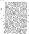
- the dielectric layers 7 according to this mode of embodiment comprise a dielectric composition.
- the dielectric composition comprises sintered particles 20 not including a high-Bi phase 8, sintered particles 30 including a high-Bi phase 8, and a grain boundary 10.
- the dielectric composition contained in the dielectric layers 7 according to this mode of embodiment is a sintered dielectric composition.
- the sintered particles 20 not including a high-Bi phase and the sintered particles 30 including a high-Bi phase are also referred to collectively below as the "sintered particles 20, 30".
- the dialectic composition comprises a high-Bi phase 8 in which the Bi concentration is at least 1.2 times the mean Bi concentration of the dielectric composition as a whole.
- the dielectric composition may also include pores (air holes) (not depicted). Oxygen is substantially absent from the pores. There is no particular limitation as to the cross-sectional area of the pores, but a value of 5% or less as a surface area proportion with respect to the dielectric composition as a whole is preferred.
- the high-Bi phase 8 may be included in the dielectric composition in any form.
- the high-Bi phase 8 may be included in the sintered particles.
- the high-Bi phase 8 may be included in the grain boundary 10.
- the high-Bi phase 8 may of course be included in both the sintered particles and the grain boundary 10.
- Bi concentration in the high-Bi phase 8 there is no particular upper limit to the Bi concentration in the high-Bi phase 8, but a value of no greater than 2.0 times the mean Bi concentration is preferred.
- the dielectric composition according to this mode of embodiment has a high-Bi phase 8, and as a result the dielectric constant when a DC bias is applied is maintained in a preferred range while the high-temperature load lifespan is also improved.
- a dielectric composition in which the high-Bi phase 8 is absent has a reduced high-temperature load lifespan and reduced reliability in comparison with a dielectric composition in which the high-Bi phase 8 is present.
- the surface area of the observation field there is no particular limitation as to the surface area of the observation field, but a surface area including around 20-50 of the sintered particles 20, 30 is preferred from the point of view of EDS analysis accuracy and analysis efficiency.
- the observation field preferably has a size of the order of 5 ⁇ m ⁇ 5 ⁇ m.
- the magnification of the observation field is preferably between 10,000 and 50,000 times.
- Composition mapping analysis is then carried out in the whole observation field by means of energy dispersive X-ray spectroscopy (EDS), and the X-ray spectrum for elemental Bi is measured.
- the mean concentration of elemental Bi included in the observation field as a whole (mean Bi concentration) is calculated from the resulting X-ray spectrum.
- a mapping image for the elemental Bi is then subjected to image processing in such a way that it is possible to distinguish regions in which the elemental Bi concentration is at least 1.2 times the mean Bi concentration (high-Bi phase 8) and regions in which the value is less than 1.2 times.
- the surface area proportion ⁇ occupied by the high-Bi phase 8 with respect to the field as a whole is then calculated from the mapping image which has undergone image processing. Specifically, the surface area proportion ⁇ with respect to the field as a whole is calculated by selecting all of the high-Bi phases in the mapping image and counting the number of pixels occupied by the selected regions.
- a high-Bi phase 8 is present somewhere in the observation field as a whole, a high-Bi phase in which the Bi concentration is at least 1.2 times the mean Bi concentration of the dielectric composition as a whole is deemed to be included. Conversely, if a high-Bi phase 8 is not present anywhere in the observation field as a whole, a high-Bi phase in which the Bi concentration is at least 1.2 times the mean Bi concentration of the dielectric composition as a whole is deemed not to be included.
- the surface area proportion ⁇ is preferably such that 0 ⁇ ⁇ ⁇ 0.150. When 0 ⁇ ⁇ ⁇ 0.150 is satisfied, it is possible to further improve the high-temperature load lifespan.
- the surface area proportion ⁇ is more preferably such that 0.001 ⁇ ⁇ ⁇ 0.150.
- the dielectric composition according to this mode of embodiment is preferably such that the molar ratio ⁇ of the Bi content with respect to the Sr content satisfies 0.125 ⁇ ⁇ ⁇ 2.00.
- ⁇ is within the abovementioned range, the dielectric constant when a DC bias is applied is further improved.
- the dielectric composition according to this mode of embodiment may include at least one selected from among La, Ce, Pr, Nd, Sm, Eu, Gd, Tb, Dy, Ho, Yb, Ba, Ca, Mg and Zn (also referred to below as the "first auxiliary component").
- the first auxiliary component By incorporating the first auxiliary component, the DC bias characteristics are further improved.
- the content of the first auxiliary component is preferably between 1 molar part and 15 molar parts, taking the Ti content of the dielectric composition as 100 molar parts. When the content of the first auxiliary component is within the abovementioned range, the DC bias characteristics are further improved.
- the content of the first auxiliary component is more preferably between 1 molar part and 10 molar parts.
- the dielectric composition according to this mode of embodiment may also include Li (also referred to below as the "second auxiliary component").
- the content of the second auxiliary component is preferably between 0.1 molar parts and 5 molar parts, taking the Ti content of the dielectric composition as 100 molar parts.
- the content of the second auxiliary component is more preferably between 1 molar part and 5 molar parts.
- the method for producing the laminated ceramic capacitor is produced in the same way as a conventional laminated ceramic capacitor, namely by preparing a green chip using a normal sheet method or printing method employing a paste, baking the green chip and then printing or transcribing external electrodes and then baking.
- the method for producing the laminated ceramic capacitor will be described in specific terms below.
- said paste may be an organic paint comprising a mixture of a dielectric starting material and an organic vehicle, or it may be an aqueous paint comprising a mixture of a dielectric starting material and an aqueous vehicle.
- the dielectric starting material it is possible to use a metal contained in the abovementioned dielectric composition, for example an oxide of a metal selected from the group consisting of Bi, Na, Sr, Ti, La, Ce, Pr, Nd, Sm, Eu, Gd, Tb, Dy, Ho, Yb, Ba, Ca, Mg, Zn, and Li, or a mixture thereof, or a composite oxide may be used.
- the dielectric starting material may be appropriately selected from various types of compounds which form the abovementioned oxides or composite oxides as a result of baking, e.g. carbonates, oxalates, nitrates, hydroxides and organometallic compounds etc. and these may be mixed for use.
- a powder having a mean particle size of the order of 0.1-3 ⁇ m is used as the dielectric starting material.
- the dielectric starting material is preferably a powder having a mean particle size of 0.1-1 ⁇ m.
- the mean particle size of the dielectric starting material may be adjusted by appropriately varying the time for which said material is mixed.
- the dielectric starting material and an organic vehicle in which a binder or the like is dissolved in an organic solvent should be mixed.
- the binder which is used in the organic vehicle may be appropriately selected from various conventional binders such as ethyl cellulose and polyvinyl butyral.
- the organic solvent which is used in the organic vehicle may be appropriately selected from various types of organic solvents such as terpineol, butyl carbitol, acetone and toluene, in accordance with the method which is used, namely the printing method or sheet method etc.
- the paste for the dielectric layers is an aqueous paint
- the dielectric starting material and an aqueous vehicle in which a water-soluble binder and a dispersant etc. are dissolved in water should be mixed.
- the water-soluble binder which is used in the aqueous vehicle and it is possible to use polyvinyl alcohol, cellulose or water-soluble acrylic resin, for example.
- the paste for the internal electrode layers is prepared by mixing a conductive material comprising various metals or alloys described above, or various types of oxide which form the conductive material after baking, organometallic compounds, resinates, and the like, with the abovementioned organic vehicle or aqueous vehicle.
- the paste for the external electrodes may be prepared in the same way as the paste for the internal electrode layers.
- the binder may be present in an amount of the order of 1-5 wt% and the organic solvent may be present in an amount of the order of 10-50 wt%, with respect to the dielectric starting material.
- the pastes may contain additives selected from various types of dispersants, plasticizers, dielectrics, and insulators etc., as required. The total content of these additives is preferably no greater than 10 wt%.
- the paste for the dielectric layers and the paste for the internal electrode layers are printed alternately and repeatedly on a substrate made of polyethylene terephthalate (PET) or the like. After the printing, the pastes are cut to a predetermined shape, after which they are peeled from the substrate to form a green chip.
- PET polyethylene terephthalate
- a green sheet is formed using the paste for the dielectric layers, and the paste for the internal electrode layers is printed on the green sheet. After this, the green sheets are peeled, stacked and cut to form a green chip.
- a debinding treatment is performed.
- the conditions of the debinding treatment there is no particular limitation as to the conditions of the debinding treatment and it should be carried out under normal conditions.
- the debinding treatment is preferably carried out under a reducing atmosphere when a base metal alone or an alloy comprising a base metal, such as Cu or Cu alloy, is used for the conductive material of the internal electrode layers.
- a base metal alone or an alloy comprising a base metal such as Cu or Cu alloy
- humidified N 2 gas or a mixed gas comprising humidified N 2 and H 2 among others.
- the temperature increase rate is preferably 0.1-100°C/hr and more preferably 1-10°C/hr.
- the holding temperature is preferably 200-500°C and more preferably 300-450°C.
- the temperature holding time is preferably 1-48 hours and more preferably 2-24 hours.
- the organic component such as the binder component is preferably removed down to around 300 ppm by means of the debinding treatment, and more preferably removed down to around 200 ppm.
- the baking atmosphere when the green chip is baked to obtain the capacitor element main body should be appropriately determined in accordance with the type of conductive material in the paste for the internal electrode layers.
- the oxygen partial pressure in the baking atmosphere is preferably set at 10 -6 to 10 -8 atm.
- the oxygen partial pressure is set at 10 -8 atm or greater, it is possible to restrict degradation of the perovskite crystal structure contained in the dielectric composition and a reduction in the high-temperature load lifespan.
- the oxygen partial pressure is set at 10 -6 atm or less, it is possible to restrict oxidation of the internal electrode layers.
- the holding temperature during baking is 900-1400°C, preferably 900-1200°C, and more preferably 1000-1100°C.
- the holding temperature is set at 900°C or greater, this makes densification more likely to progress adequately due to baking.
- the holding temperature is set at 1200°C or less, this facilitates suppressing diffusion of the various materials forming the internal electrode layers and abnormal sintering of the internal electrode layers. By suppressing abnormal sintering of the internal electrode layers, this facilitates preventing breakage of the internal electrodes. By suppressing diffusion of the various materials forming the internal electrode layers, this facilitates preventing a reduction in the high-temperature load lifespan.
- the baking atmosphere is preferably a reducing atmosphere so as to restrict oxidation of the internal electrode layers.
- the atmospheric gas A mixed gas comprising N 2 and H 2 which is humidified is preferably used as the atmospheric gas, for example.
- the baking time is no particular limitation as to the baking time.
- Annealing may be carried out after the baking during the production of the laminated ceramic capacitor according to this mode of embodiment.
- the annealing should be carried out under normal conditions.
- There is no particular limitation as to the annealing atmosphere but an atmosphere in which the dielectric layers are oxidized and the internal electrode layers are not oxidized is preferred.
- Humidified N 2 gas or a mixed gas comprising humidified N 2 and H 2 etc. may be used, for example.
- a wetter or the like should be used in order to humidify the N 2 gas or the mixed gas comprising N 2 and H 2 etc. in the abovementioned debinding treatment, baking and annealing.
- the water temperature is preferably around 20-90°C.
- the debinding treatment, baking and annealing processes may be carried out successively or independently.
- the following procedure is preferred, namely that the debinding treatment is performed, after which the atmosphere is modified without cooling and then baking is carried out by raising the temperature to the holding temperature for baking.
- the following procedure is preferred, namely that during baking the temperature is raised under an N 2 gas atmosphere to the holding temperature for the debinding treatment, after which the atmosphere is modified to the atmosphere for baking, and after the atmosphere has been modified, temperature increase is continued to the holding temperature for baking.
- cooling is performed to the holding temperature for the debinding treatment, after which the atmosphere is once again modified to an N 2 gas atmosphere and cooling is further continued.
- the abovementioned N 2 gas may or may not be humidified.
- the end surfaces of the capacitor element main body obtained in this way are polished by means of barrel polishing or sandblasting, for example, the paste for the external electrodes is printed or transcribed thereon, baking is carried out and the external electrodes are formed.
- the paste for the external electrodes is preferably baked at 600-800°C for around 10 minutes to 1 hour under a humidified mixed gas comprising N 2 and H 2 , for example.
- a coating layer is then formed on the external electrode surface, as required.
- the coating layer is formed by means of plating or the like.
- a laminated ceramic capacitor according to a mode of embodiment of the present invention and a method for producing same have been described above, but the present invention is in no way limited to this mode of embodiment and various modes may of course be implemented within a scope that does not depart from the essential point of the present invention.
- the dielectric element, electronic component and laminated electronic component according to the present invention are advantageously used in a location where a relatively high rated voltage is applied.
- they may be advantageously used in a power supply circuit having a high rated voltage, such as in a DC-DC converter or an AC-DC inverter, for example.
- the laminated ceramic capacitor may be used in a snubber capacitor for circuit protection for which there is a need for a high dielectric constant when a high DC bias is applied, or it may be used in a smoothing capacitor for an AC-DC inverter that converts alternating current to direct current.
- the laminated ceramic capacitor according to this mode of embodiment is mounted on a printed circuit board or the like by means of soldering etc.
- the printed circuit board is then used in various electronic devices, e.g. a digital television or a modem etc.
- the dielectric composition according to the present invention does not contain lead.
- the inventive dielectric composition, dielectric element, electronic component and laminated electronic component are therefore also superior from an environmental point of view.
- the present invention will be described below in further detail with the aid of exemplary embodiments and comparative examples. However, the present invention is not limited by the following exemplary embodiments.
- the DC field applied to the dielectric composition, dielectric element, electronic component and laminated electronic component is referred to as a DC (direct current) bias.
- the rate of change in the dielectric constant before and after application of the DC bias is referred to as the DC bias characteristics.
- the DC bias characteristics are better the smaller the absolute value of the rate of change of the dielectric constant.
- the following starting material powders were prepared as starting materials for producing dielectric layers: bismuth oxide (Bi 2 O 3 ), sodium carbonate (Na 2 CO 3 ), strontium carbonate (SrCO 3 ), barium carbonate (BaCO 3 ), calcium carbonate (CaCO 3 ), magnesium carbonate (MgCO 3 ), zinc oxide (ZnO), lanthanum hydroxide (La(OH) 3 ), neodymium oxide (Nd 2 O 3 ) , samarium oxide (Sm 2 O 3 ), gadolinium oxide (Gd 2 O 3 ) and titanium oxide (TiO 2 ).
- the weighed starting material powders were then wet-mixed using a ball mill, after which the resulting mixtures were calcined for 2 hours under the air at 750°C-850°C to obtain calcined powders.
- Li 2 CO 3 was then prepared as an Li starting material powder constituting a second auxiliary component.
- the starting material powder was weighed out in such a way that the compositions after baking conformed to the compositions shown in table 1, and said starting material powder was mixed with the abovementioned calcined powders to obtain mixed powders.
- the paste for the internal electrode layers was coated on the ceramic green sheets by means of screen printing to print the internal electrode layers.
- the ceramic green sheets on which the internal electrode layers had been printed were then stacked, after which they were cut to a predetermined shape, whereby laminated green chips were prepared.
- the laminated green chips were subjected to debinding at 300°C-500°C to remove the organic component down to around 300 ppm. After the debinding, baking was carried out under the atmosphere or under a reducing atmosphere at a baking temperature of 900°C-1400°C. The baking time was varied as appropriate.
- a mixed gas comprising humidified N 2 and H 2 was used as the atmospheric gas when baking was carried out under a reducing atmosphere.
- the end surfaces of the resulting laminated ceramic baked articles were polished, after which In-Ga was applied thereto as the external electrodes, and samples of the laminated ceramic capacitor shown in fig. 1 were obtained.
- the size of the resulting laminated ceramic capacitor samples was 3.2 mm ⁇ 1.6 mm ⁇ 0.6 mm, the thickness of the dielectric layers was 20 ⁇ m, the thickness of the internal electrode layers was 1.5 ⁇ m, and there were four dielectric layers interposed between the internal electrode layers.
- the dielectric layers of the laminated ceramic baked articles comprised a composition having a perovskite crystal structure.
- the surface area proportion of the high-Bi phase and the mean concentration of elemental Bi were then measured using the method described below for each of the laminated ceramic baked articles obtained.
- the dielectric constant, DC bias characteristics and high-temperature load lifespan were then measured using the method described below.
- a cross section at the intersection of the internal electrode layers was first of all cut from the laminated ceramic baked articles obtained, and the cross sections which had been cut were cut into flakes by means of a gallium ion beam to prepare samples for cross-sectional observation.
- the cross section of the dielectric layers cut at the position of intersection with the internal electrode layers was observed by means of scanning transmission electron microscopy (STEM). It should be noted that the observation field was 5 ⁇ m ⁇ 5 ⁇ m and the magnification was 30 000 times. Mapping analysis was performed in the whole field set in the cross section of the dielectric layers by means of energy dispersive X-ray spectroscopy (EDS), and the X-ray spectrum of elemental Bi was measured. The mean concentration of elemental Bi included in the whole field was calculated from the resulting X-ray spectrum.
- STEM scanning transmission electron microscopy
- a mapping image for the elemental Bi was then subjected to image processing in such a way as to distinguish a phase in which the elemental Bi concentration was at least 1.2 times the mean concentration (high-Bi phase) and a phase in which the value was less than 1.2 times.
- the surface area proportion ⁇ occupied by the high-Bi phase in the field as a whole was then calculated from the image which had undergone image processing.
- the surface area proportion ⁇ with respect to the field as a whole was calculated by counting the number of pixels occupied by the high-Bi phase in the image which had undergone image processing, and dividing this number by the total number of pixels in the field as a whole. The results are shown in table 1.
- the capacitance of the laminated ceramic capacitor samples was measured at 25°C and a frequency of 1 kHz by inputting a signal having an input signal level (measurement voltage) of 1 Vrms using a digital LCR meter (Hewlett-Packard; 4284A).
- the dielectric constant ⁇ 1 (no units) was then calculated from the measured capacitance, surface area of facing electrodes and interlayer distance.
- the mean value calculated from 10 laminated ceramic capacitor samples was used as the dielectric constant ⁇ 1. The results are shown in table 1.
- the dielectric constant ⁇ 2 (no units) was calculated from the capacitance measured from conditions of frequency 1 kHz and input signal level (measurement voltage) 1.0 Vrms, surface area of facing electrodes and interlayer distance, while a DC bias generator (GLASSMAN HIGH VOLTAGE; WX10P90) was connected to a digital LCR meter (Hewlett-Packard; 4284A) and a DC bias of 8 V/ ⁇ m was applied to the laminated ceramic capacitor samples.
- the mean value calculated from 10 laminated ceramic capacitor samples was used as the dielectric constant ⁇ 2.
- a value of 800 or greater for the dielectric constant ⁇ 2 was deemed to be good and a value of 1000 or greater was deemed to be better in the present exemplary embodiments. The results are shown in table 1.
- the DC bias characteristics were calculated by means of the following formula (1) using the dielectric constant ⁇ 1 and the dielectric constant ⁇ 2. Although superior DC bias characteristics are not essential for achieving the aim of the present invention, a smaller absolute value for the DC bias characteristics is preferable. DC bias characteristics within ⁇ 30% were deemed to be good in the present exemplary embodiments. It should be noted that it is not realistic for the DC bias characteristics to exceed +30%. There is therefore essentially no upper limit to the preferred range for the DC bias characteristics.
- DC bias characteristics % 100 ⁇ ⁇ 2 ⁇ ⁇ 1 / ⁇ 1
- the high-temperature load lifespan was measured for the laminated ceramic capacitor samples by maintaining a state of DC voltage application under an electric field of 50 V/ ⁇ m at 150°C.
- the high-temperature load lifespan was defined as the time from the start of DC voltage application until the insulation resistance fell to a single digit.
- the high-temperature load lifespan was measured for 10 laminated ceramic capacitor samples and the mean value thereof was calculated. A value of 20 hours or greater was deemed to be good, a value of 30 hours or greater was deemed to be better, and a value of 35 hours or greater was deemed to be even better in the present exemplary embodiments. The results are shown in table 1.
- the laminated ceramic capacitors according to Comparative Examples 1 and 2 in which a high-Bi phase was not present exhibited a high-temperature load lifespan of less than 20 hours.
- the laminated ceramic capacitors according to Exemplary Embodiments 6-17 comprising between 1 molar part and 15 molar parts of the first auxiliary component exhibited DC bias characteristics within ⁇ 30%. That is to say, the laminated ceramic capacitor samples comprising the first auxiliary component exhibited a good dielectric constant ⁇ 2 when a DC bias was applied, a good high-temperature load lifespan, and also good DC bias characteristics.
- the laminated ceramic capacitors according to Exemplary Embodiments 9 and 10 comprising between 0.1 molar parts and 5 molar parts of the second auxiliary component exhibited a high-temperature load lifespan of 35 hours or greater, and this was even better.
Landscapes
- Engineering & Computer Science (AREA)
- Chemical & Material Sciences (AREA)
- Ceramic Engineering (AREA)
- Manufacturing & Machinery (AREA)
- Power Engineering (AREA)
- Structural Engineering (AREA)
- Organic Chemistry (AREA)
- Materials Engineering (AREA)
- Inorganic Chemistry (AREA)
- Microelectronics & Electronic Packaging (AREA)
- Physics & Mathematics (AREA)
- Thermal Sciences (AREA)
- Ceramic Capacitors (AREA)
- Fixed Capacitors And Capacitor Manufacturing Machines (AREA)
- Inorganic Insulating Materials (AREA)
Claims (15)
- Dielektrische Zusammensetzung, die eine Perowskit-Kristallstruktur aufweist, die mindestens Bi, Na, Sr und Ti enthält, wobeidie dielektrische Zusammensetzung eine Bi-reiche Phase enthält, in der die Bi-Konzentration mindestens das 1,2-Fache der mittleren Bi-Konzentration in der dielektrischen Zusammensetzung insgesamt beträgt, dadurch gekennzeichnet, dass0 < α ≤ 0,150 ist, wobei α der Oberflächenanteil der Bi-reichen Phase im Querschnitt der dielektrischen Zusammensetzung, bezogen auf den gesamten Querschnitt.
- Dielektrische Zusammensetzung nach Anspruch 1, wobei 0,125 ≤ β ≤ 2,000, wobei β das Molverhältnis von Bi zu Sr in der dielektrischen Zusammensetzung ist.
- Dielektrische Zusammensetzung nach einem der Ansprüche 1 bis 2, die mindestens eines von La, Ce, Pr, Nd, Sm, Eu, Gd, Tb, Dy, Ho, Yb, Ba, Ca, Mg und Zn umfasst.
- Dielektrische Zusammensetzung nach Anspruch 3, wobei der Gehalt des mindestens einen von La, Ce, Pr, Nd, Sm, Eu, Gd, Tb, Dy, Ho, Yb, Ba, Ca, Mg und Zn zwischen 1 Molteil und 15 Molteilen liegt, wobei der Ti-Gehalt der dielektrischen Zusammensetzung als 100 Molteile genommen wird.
- Dielektrische Zusammensetzung nach einem der Ansprüche 1 bis 4, die Li umfasst,
wobei der Li-Gehalt zwischen 0,1 Molteilen und 5 Molteilen liegt, wobei der Ti-Gehalt der dielektrischen Zusammensetzung als 100 Molteile genommen wird. - Dielektrisches Element, das mit der dielektrischen Zusammensetzung nach einem der Ansprüche 1 bis 5 versehen ist.
- Elektronische Komponente, die mit einer dielektrischen Schicht, die die dielektrische Zusammensetzung nach einem der Ansprüche 1 bis 5 umfasst, versehen ist.
- Laminierte elektronische Komponente mit einem laminierten Teil, der durch alternierendes Laminieren einer internen Elektrodenschicht und einer dielektrischen Schicht, die die dielektrische Zusammensetzung nach einem der Ansprüche 1 bis 5 umfasst, gebildet ist.
- Einplattenkondensator (100), der die dielektrische Zusammensetzung nach einem der Ansprüche 1 bis 5 umfasst.
- Laminierter keramischer Kondensator (200), umfassend:- einen Kondensatorelement-Hauptkörper (5) mit einer Struktur, in der dielektrische Schichten (7), die die dielektrische Zusammensetzung nach einem der Ansprüche 1 bis 5 umfassen, und interne Elektrodenschichten (6A, 6B) alternierend gestapelt sind, und- ein Paar von Anschlusselektroden (11A, 11B), die an beiden Enden des Kondensatorelement-Hauptkörpers (5) ausgebildet sind und mit freiliegenden Endflächen der alternierend angeordneten internen Elektrodenschichten (6A, 6B) verbunden sind, wodurch ein Kondensatorschaltkreis gebildet wird.
- Laminierter keramischer Kondensator (200) nach Anspruch 10,
wobei ein leitfähiges Material der internen Elektrodenschichten (6A, 6B) Cu oder Cu-Legierung umfasst. - Laminierter keramischer Kondensator (200) nach Anspruch 10 oder Anspruch 11,
wobei ein Nichtedelmetall als leitfähiges Material für die internen Elektrodenschichten (6A, 6B) verwendet wird. - Laminierter keramischer Kondensator (200) nach einem der Ansprüche 10 bis 12, wobei die externen Elektroden (11A, 11B) Cu oder Cu-Legierung umfassen.
- Verfahren zur Herstellung des keramischen Kondensators (200), das die folgenden Schritte umfasst:- Herstellen eines Grünchips mit Hilfe eines Folienverfahrens oder eines Druckverfahrens unter Verwendung einer Paste für dielektrische Schichten und einer Paste für interne Elektroden, wobei es sich bei der Paste für die dielektrischen Schichten um einen organischen Aufstrich handelt, die eine Mischung eines dielektrischen Ausgangsstoffs und eines organischen Vehikels umfasst, oder wobei es sich bei der Paste für die dielektrischen Schichten um eine wässrigen Aufstrich handelt, die eine Mischung eines dielektrischen Ausgangsstoffs und eines wässrigen Vehikels umfasst,- Durchführen einer Entbinderungsbehandlung,- Brennen des Grünchips,- dann Drucken oder Übertragen von externen Elektroden,- dann Brennen,wobei die Ausgangsstoffe so gewählt werden, dass die gebrannte dielektrische Zusammensetzung eine Perowskit-Kristallstruktur aufweist, die mindestens Bi, Na, Sr und Ti enthält,
wobei die dielektrische Zusammensetzung eine Bi-reiche Phase enthält, in der die Bi-Konzentration mindestens das 1,2-Fache der mittleren Bi-Konzentration in der dielektrischen Zusammensetzung insgesamt beträgt, in der 0 < α ≤ 0,150 ist, wobei α der Oberflächenanteil der Bi-reichen Phase im Querschnitt der dielektrischen Zusammensetzung, bezogen auf den gesamten Querschnitt. - Verfahren nach Anspruch 14, wobei ein Nichtedelmetall alleine oder eine ein Nichtedelmetall umfassende Legierung, wie Cu oder Cu-Legierung, für ein leitfähiges Material der inneren Elektrodenschichten verwendet wird.
Applications Claiming Priority (2)
| Application Number | Priority Date | Filing Date | Title |
|---|---|---|---|
| JP2015143407 | 2015-07-17 | ||
| PCT/EP2016/063836 WO2017012788A1 (en) | 2015-07-17 | 2016-06-16 | Dielectric composition, dielectric element, electronic component and laminated electronic component |
Publications (2)
| Publication Number | Publication Date |
|---|---|
| EP3326182A1 EP3326182A1 (de) | 2018-05-30 |
| EP3326182B1 true EP3326182B1 (de) | 2022-03-23 |
Family
ID=56132943
Family Applications (1)
| Application Number | Title | Priority Date | Filing Date |
|---|---|---|---|
| EP16729573.2A Not-in-force EP3326182B1 (de) | 2015-07-17 | 2016-06-16 | Dielektrische zusammensetzung, dielektrisches element, elektronische komponente und laminierte elektronische komponente |
Country Status (6)
| Country | Link |
|---|---|
| US (1) | US10497514B2 (de) |
| EP (1) | EP3326182B1 (de) |
| JP (1) | JP6655706B2 (de) |
| KR (1) | KR102115680B1 (de) |
| CN (1) | CN107851512B (de) |
| WO (1) | WO2017012788A1 (de) |
Families Citing this family (7)
| Publication number | Priority date | Publication date | Assignee | Title |
|---|---|---|---|---|
| EP3326178B1 (de) * | 2015-07-17 | 2019-05-22 | TDK Electronics AG | Dielektrische zusammensetzung, dielektrisches element, elektronische komponente und laminierte elektronische komponente |
| EP3326177B1 (de) * | 2015-07-17 | 2022-03-09 | TDK Electronics AG | Mehrschichtiger keramikkondensator |
| CN107851512B (zh) * | 2015-07-17 | 2020-04-17 | 埃普科斯股份有限公司 | 介电组成、介电元件、电子部件和层压电子部件 |
| KR102096228B1 (ko) * | 2015-07-17 | 2020-04-03 | 티디케이 일렉트로닉스 아게 | 유전체 조성물, 유전체 소자, 전자 부품 및 적층 전자 부품 |
| US10438745B2 (en) * | 2015-07-17 | 2019-10-08 | Tdk Electronics Ag | Dielectric composition, dielectric element, electronic component and laminated electronic component |
| EP3326184B1 (de) * | 2015-07-17 | 2019-11-20 | TDK Electronics AG | Dielektrische zusammensetzung, dielektrisches element, elektronische komponente und mehrschichtige elektronische komponente |
| DE102020118857B4 (de) | 2020-07-16 | 2023-10-26 | Tdk Electronics Ag | Vielschichtkondensator |
Family Cites Families (16)
| Publication number | Priority date | Publication date | Assignee | Title |
|---|---|---|---|---|
| JPS4959297A (de) | 1972-10-12 | 1974-06-08 | ||
| US4119554A (en) | 1976-05-06 | 1978-10-10 | Tdk Electronics Co., Ltd. | Ceramic dielectric composition containing alkali metal oxide |
| JP2000223351A (ja) | 1999-01-28 | 2000-08-11 | Murata Mfg Co Ltd | 積層セラミックコンデンサ |
| MY124934A (en) * | 2000-06-30 | 2006-07-31 | Taiyo Yuden Kk | Dielectric ceramic composition and ceramic capacitor |
| JP2002080276A (ja) * | 2000-06-30 | 2002-03-19 | Taiyo Yuden Co Ltd | 誘電体磁器組成物及び磁器コンデンサ |
| JP2005022891A (ja) * | 2003-06-30 | 2005-01-27 | Kyocera Corp | 誘電体磁器および積層型電子部品 |
| US8076257B1 (en) * | 2008-04-23 | 2011-12-13 | MRA Laboratories, Inc | High temperature ceramic dielectric composition and capacitors made from the composition |
| JP5109872B2 (ja) | 2008-08-27 | 2012-12-26 | 株式会社村田製作所 | 積層セラミックコンデンサおよびその製造方法 |
| JP6102410B2 (ja) | 2013-03-28 | 2017-03-29 | Tdk株式会社 | 誘電体磁器組成物、および誘電体素子 |
| JP6839086B2 (ja) | 2015-01-13 | 2021-03-03 | トゥルーデル メディカル インターナショナル | 呼吸器インターフェース |
| EP3326177B1 (de) * | 2015-07-17 | 2022-03-09 | TDK Electronics AG | Mehrschichtiger keramikkondensator |
| EP3326184B1 (de) * | 2015-07-17 | 2019-11-20 | TDK Electronics AG | Dielektrische zusammensetzung, dielektrisches element, elektronische komponente und mehrschichtige elektronische komponente |
| US10438745B2 (en) * | 2015-07-17 | 2019-10-08 | Tdk Electronics Ag | Dielectric composition, dielectric element, electronic component and laminated electronic component |
| KR102096228B1 (ko) * | 2015-07-17 | 2020-04-03 | 티디케이 일렉트로닉스 아게 | 유전체 조성물, 유전체 소자, 전자 부품 및 적층 전자 부품 |
| CN107851512B (zh) * | 2015-07-17 | 2020-04-17 | 埃普科斯股份有限公司 | 介电组成、介电元件、电子部件和层压电子部件 |
| EP3326178B1 (de) * | 2015-07-17 | 2019-05-22 | TDK Electronics AG | Dielektrische zusammensetzung, dielektrisches element, elektronische komponente und laminierte elektronische komponente |
-
2016
- 2016-06-16 CN CN201680042073.4A patent/CN107851512B/zh active Active
- 2016-06-16 KR KR1020187004457A patent/KR102115680B1/ko active Active
- 2016-06-16 WO PCT/EP2016/063836 patent/WO2017012788A1/en not_active Ceased
- 2016-06-16 US US15/745,696 patent/US10497514B2/en active Active
- 2016-06-16 EP EP16729573.2A patent/EP3326182B1/de not_active Not-in-force
- 2016-06-16 JP JP2018501899A patent/JP6655706B2/ja active Active
Also Published As
| Publication number | Publication date |
|---|---|
| WO2017012788A1 (en) | 2017-01-26 |
| JP2018529221A (ja) | 2018-10-04 |
| JP6655706B2 (ja) | 2020-02-26 |
| CN107851512A (zh) | 2018-03-27 |
| CN107851512B (zh) | 2020-04-17 |
| US10497514B2 (en) | 2019-12-03 |
| KR102115680B1 (ko) | 2020-05-26 |
| KR20180029244A (ko) | 2018-03-20 |
| EP3326182A1 (de) | 2018-05-30 |
| US20180211781A1 (en) | 2018-07-26 |
Similar Documents
| Publication | Publication Date | Title |
|---|---|---|
| EP3326183B1 (de) | Dielektrische zusammensetzung, dielektrisches element, elektronische komponente und laminierte elektronische komponente | |
| EP3326177B1 (de) | Mehrschichtiger keramikkondensator | |
| EP3326182B1 (de) | Dielektrische zusammensetzung, dielektrisches element, elektronische komponente und laminierte elektronische komponente | |
| EP3326178B1 (de) | Dielektrische zusammensetzung, dielektrisches element, elektronische komponente und laminierte elektronische komponente | |
| EP3326184B1 (de) | Dielektrische zusammensetzung, dielektrisches element, elektronische komponente und mehrschichtige elektronische komponente | |
| EP3326185B1 (de) | Dielektrische zusammensetzung, dielektrisches element, elektronische komponente und laminierte elektronische komponente | |
| EP3304571B1 (de) | Dielektrische zusammensetzung auf basis von wismut-natriumstrontiumtitanat, dielektrisches element, elektronische komponente und laminierte elektronische komponente davon | |
| EP3304572B1 (de) | Dielektrische zusammensetzung auf basis von wismut-natriumstrontiumtitanat, dielektrisches element, elektronische komponente und laminierte elektronische komponente davon |
Legal Events
| Date | Code | Title | Description |
|---|---|---|---|
| STAA | Information on the status of an ep patent application or granted ep patent |
Free format text: STATUS: THE INTERNATIONAL PUBLICATION HAS BEEN MADE |
|
| PUAI | Public reference made under article 153(3) epc to a published international application that has entered the european phase |
Free format text: ORIGINAL CODE: 0009012 |
|
| STAA | Information on the status of an ep patent application or granted ep patent |
Free format text: STATUS: REQUEST FOR EXAMINATION WAS MADE |
|
| 17P | Request for examination filed |
Effective date: 20180215 |
|
| AK | Designated contracting states |
Kind code of ref document: A1 Designated state(s): AL AT BE BG CH CY CZ DE DK EE ES FI FR GB GR HR HU IE IS IT LI LT LU LV MC MK MT NL NO PL PT RO RS SE SI SK SM TR |
|
| AX | Request for extension of the european patent |
Extension state: BA ME |
|
| DAV | Request for validation of the european patent (deleted) | ||
| DAX | Request for extension of the european patent (deleted) | ||
| RAP1 | Party data changed (applicant data changed or rights of an application transferred) |
Owner name: TDK ELECTRONICS AG |
|
| GRAP | Despatch of communication of intention to grant a patent |
Free format text: ORIGINAL CODE: EPIDOSNIGR1 |
|
| STAA | Information on the status of an ep patent application or granted ep patent |
Free format text: STATUS: GRANT OF PATENT IS INTENDED |
|
| INTG | Intention to grant announced |
Effective date: 20210420 |
|
| GRAJ | Information related to disapproval of communication of intention to grant by the applicant or resumption of examination proceedings by the epo deleted |
Free format text: ORIGINAL CODE: EPIDOSDIGR1 |
|
| STAA | Information on the status of an ep patent application or granted ep patent |
Free format text: STATUS: REQUEST FOR EXAMINATION WAS MADE |
|
| INTC | Intention to grant announced (deleted) | ||
| GRAP | Despatch of communication of intention to grant a patent |
Free format text: ORIGINAL CODE: EPIDOSNIGR1 |
|
| STAA | Information on the status of an ep patent application or granted ep patent |
Free format text: STATUS: GRANT OF PATENT IS INTENDED |
|
| INTG | Intention to grant announced |
Effective date: 20210917 |
|
| GRAS | Grant fee paid |
Free format text: ORIGINAL CODE: EPIDOSNIGR3 |
|
| GRAA | (expected) grant |
Free format text: ORIGINAL CODE: 0009210 |
|
| STAA | Information on the status of an ep patent application or granted ep patent |
Free format text: STATUS: THE PATENT HAS BEEN GRANTED |
|
| AK | Designated contracting states |
Kind code of ref document: B1 Designated state(s): AL AT BE BG CH CY CZ DE DK EE ES FI FR GB GR HR HU IE IS IT LI LT LU LV MC MK MT NL NO PL PT RO RS SE SI SK SM TR |
|
| REG | Reference to a national code |
Ref country code: GB Ref legal event code: FG4D |
|
| REG | Reference to a national code |
Ref country code: CH Ref legal event code: EP |
|
| REG | Reference to a national code |
Ref country code: DE Ref legal event code: R096 Ref document number: 602016070257 Country of ref document: DE |
|
| REG | Reference to a national code |
Ref country code: IE Ref legal event code: FG4D |
|
| REG | Reference to a national code |
Ref country code: AT Ref legal event code: REF Ref document number: 1478024 Country of ref document: AT Kind code of ref document: T Effective date: 20220415 |
|
| REG | Reference to a national code |
Ref country code: LT Ref legal event code: MG9D |
|
| REG | Reference to a national code |
Ref country code: NL Ref legal event code: MP Effective date: 20220323 |
|
| PG25 | Lapsed in a contracting state [announced via postgrant information from national office to epo] |
Ref country code: SE Free format text: LAPSE BECAUSE OF FAILURE TO SUBMIT A TRANSLATION OF THE DESCRIPTION OR TO PAY THE FEE WITHIN THE PRESCRIBED TIME-LIMIT Effective date: 20220323 Ref country code: RS Free format text: LAPSE BECAUSE OF FAILURE TO SUBMIT A TRANSLATION OF THE DESCRIPTION OR TO PAY THE FEE WITHIN THE PRESCRIBED TIME-LIMIT Effective date: 20220323 Ref country code: NO Free format text: LAPSE BECAUSE OF FAILURE TO SUBMIT A TRANSLATION OF THE DESCRIPTION OR TO PAY THE FEE WITHIN THE PRESCRIBED TIME-LIMIT Effective date: 20220623 Ref country code: LT Free format text: LAPSE BECAUSE OF FAILURE TO SUBMIT A TRANSLATION OF THE DESCRIPTION OR TO PAY THE FEE WITHIN THE PRESCRIBED TIME-LIMIT Effective date: 20220323 Ref country code: HR Free format text: LAPSE BECAUSE OF FAILURE TO SUBMIT A TRANSLATION OF THE DESCRIPTION OR TO PAY THE FEE WITHIN THE PRESCRIBED TIME-LIMIT Effective date: 20220323 Ref country code: BG Free format text: LAPSE BECAUSE OF FAILURE TO SUBMIT A TRANSLATION OF THE DESCRIPTION OR TO PAY THE FEE WITHIN THE PRESCRIBED TIME-LIMIT Effective date: 20220623 |
|
| REG | Reference to a national code |
Ref country code: AT Ref legal event code: MK05 Ref document number: 1478024 Country of ref document: AT Kind code of ref document: T Effective date: 20220323 |
|
| PG25 | Lapsed in a contracting state [announced via postgrant information from national office to epo] |
Ref country code: LV Free format text: LAPSE BECAUSE OF FAILURE TO SUBMIT A TRANSLATION OF THE DESCRIPTION OR TO PAY THE FEE WITHIN THE PRESCRIBED TIME-LIMIT Effective date: 20220323 Ref country code: GR Free format text: LAPSE BECAUSE OF FAILURE TO SUBMIT A TRANSLATION OF THE DESCRIPTION OR TO PAY THE FEE WITHIN THE PRESCRIBED TIME-LIMIT Effective date: 20220624 Ref country code: FI Free format text: LAPSE BECAUSE OF FAILURE TO SUBMIT A TRANSLATION OF THE DESCRIPTION OR TO PAY THE FEE WITHIN THE PRESCRIBED TIME-LIMIT Effective date: 20220323 |
|
| PG25 | Lapsed in a contracting state [announced via postgrant information from national office to epo] |
Ref country code: NL Free format text: LAPSE BECAUSE OF FAILURE TO SUBMIT A TRANSLATION OF THE DESCRIPTION OR TO PAY THE FEE WITHIN THE PRESCRIBED TIME-LIMIT Effective date: 20220323 |
|
| PG25 | Lapsed in a contracting state [announced via postgrant information from national office to epo] |
Ref country code: SM Free format text: LAPSE BECAUSE OF FAILURE TO SUBMIT A TRANSLATION OF THE DESCRIPTION OR TO PAY THE FEE WITHIN THE PRESCRIBED TIME-LIMIT Effective date: 20220323 Ref country code: SK Free format text: LAPSE BECAUSE OF FAILURE TO SUBMIT A TRANSLATION OF THE DESCRIPTION OR TO PAY THE FEE WITHIN THE PRESCRIBED TIME-LIMIT Effective date: 20220323 Ref country code: RO Free format text: LAPSE BECAUSE OF FAILURE TO SUBMIT A TRANSLATION OF THE DESCRIPTION OR TO PAY THE FEE WITHIN THE PRESCRIBED TIME-LIMIT Effective date: 20220323 Ref country code: PT Free format text: LAPSE BECAUSE OF FAILURE TO SUBMIT A TRANSLATION OF THE DESCRIPTION OR TO PAY THE FEE WITHIN THE PRESCRIBED TIME-LIMIT Effective date: 20220725 Ref country code: ES Free format text: LAPSE BECAUSE OF FAILURE TO SUBMIT A TRANSLATION OF THE DESCRIPTION OR TO PAY THE FEE WITHIN THE PRESCRIBED TIME-LIMIT Effective date: 20220323 Ref country code: EE Free format text: LAPSE BECAUSE OF FAILURE TO SUBMIT A TRANSLATION OF THE DESCRIPTION OR TO PAY THE FEE WITHIN THE PRESCRIBED TIME-LIMIT Effective date: 20220323 Ref country code: CZ Free format text: LAPSE BECAUSE OF FAILURE TO SUBMIT A TRANSLATION OF THE DESCRIPTION OR TO PAY THE FEE WITHIN THE PRESCRIBED TIME-LIMIT Effective date: 20220323 Ref country code: AT Free format text: LAPSE BECAUSE OF FAILURE TO SUBMIT A TRANSLATION OF THE DESCRIPTION OR TO PAY THE FEE WITHIN THE PRESCRIBED TIME-LIMIT Effective date: 20220323 |
|
| PG25 | Lapsed in a contracting state [announced via postgrant information from national office to epo] |
Ref country code: PL Free format text: LAPSE BECAUSE OF FAILURE TO SUBMIT A TRANSLATION OF THE DESCRIPTION OR TO PAY THE FEE WITHIN THE PRESCRIBED TIME-LIMIT Effective date: 20220323 Ref country code: IS Free format text: LAPSE BECAUSE OF FAILURE TO SUBMIT A TRANSLATION OF THE DESCRIPTION OR TO PAY THE FEE WITHIN THE PRESCRIBED TIME-LIMIT Effective date: 20220723 Ref country code: AL Free format text: LAPSE BECAUSE OF FAILURE TO SUBMIT A TRANSLATION OF THE DESCRIPTION OR TO PAY THE FEE WITHIN THE PRESCRIBED TIME-LIMIT Effective date: 20220323 |
|
| REG | Reference to a national code |
Ref country code: DE Ref legal event code: R097 Ref document number: 602016070257 Country of ref document: DE |
|
| PLBE | No opposition filed within time limit |
Free format text: ORIGINAL CODE: 0009261 |
|
| STAA | Information on the status of an ep patent application or granted ep patent |
Free format text: STATUS: NO OPPOSITION FILED WITHIN TIME LIMIT |
|
| PG25 | Lapsed in a contracting state [announced via postgrant information from national office to epo] |
Ref country code: MC Free format text: LAPSE BECAUSE OF FAILURE TO SUBMIT A TRANSLATION OF THE DESCRIPTION OR TO PAY THE FEE WITHIN THE PRESCRIBED TIME-LIMIT Effective date: 20220323 Ref country code: DK Free format text: LAPSE BECAUSE OF FAILURE TO SUBMIT A TRANSLATION OF THE DESCRIPTION OR TO PAY THE FEE WITHIN THE PRESCRIBED TIME-LIMIT Effective date: 20220323 |
|
| REG | Reference to a national code |
Ref country code: CH Ref legal event code: PL |
|
| REG | Reference to a national code |
Ref country code: BE Ref legal event code: MM Effective date: 20220630 |
|
| 26N | No opposition filed |
Effective date: 20230102 |
|
| GBPC | Gb: european patent ceased through non-payment of renewal fee |
Effective date: 20220623 |
|
| PG25 | Lapsed in a contracting state [announced via postgrant information from national office to epo] |
Ref country code: LU Free format text: LAPSE BECAUSE OF NON-PAYMENT OF DUE FEES Effective date: 20220616 Ref country code: LI Free format text: LAPSE BECAUSE OF NON-PAYMENT OF DUE FEES Effective date: 20220630 Ref country code: IE Free format text: LAPSE BECAUSE OF NON-PAYMENT OF DUE FEES Effective date: 20220616 Ref country code: FR Free format text: LAPSE BECAUSE OF NON-PAYMENT OF DUE FEES Effective date: 20220630 Ref country code: CH Free format text: LAPSE BECAUSE OF NON-PAYMENT OF DUE FEES Effective date: 20220630 |
|
| PG25 | Lapsed in a contracting state [announced via postgrant information from national office to epo] |
Ref country code: SI Free format text: LAPSE BECAUSE OF FAILURE TO SUBMIT A TRANSLATION OF THE DESCRIPTION OR TO PAY THE FEE WITHIN THE PRESCRIBED TIME-LIMIT Effective date: 20220323 Ref country code: GB Free format text: LAPSE BECAUSE OF NON-PAYMENT OF DUE FEES Effective date: 20220623 Ref country code: BE Free format text: LAPSE BECAUSE OF NON-PAYMENT OF DUE FEES Effective date: 20220630 |
|
| P01 | Opt-out of the competence of the unified patent court (upc) registered |
Effective date: 20230521 |
|
| PG25 | Lapsed in a contracting state [announced via postgrant information from national office to epo] |
Ref country code: IT Free format text: LAPSE BECAUSE OF FAILURE TO SUBMIT A TRANSLATION OF THE DESCRIPTION OR TO PAY THE FEE WITHIN THE PRESCRIBED TIME-LIMIT Effective date: 20220323 |
|
| PG25 | Lapsed in a contracting state [announced via postgrant information from national office to epo] |
Ref country code: HU Free format text: LAPSE BECAUSE OF FAILURE TO SUBMIT A TRANSLATION OF THE DESCRIPTION OR TO PAY THE FEE WITHIN THE PRESCRIBED TIME-LIMIT; INVALID AB INITIO Effective date: 20160616 |
|
| PG25 | Lapsed in a contracting state [announced via postgrant information from national office to epo] |
Ref country code: MK Free format text: LAPSE BECAUSE OF FAILURE TO SUBMIT A TRANSLATION OF THE DESCRIPTION OR TO PAY THE FEE WITHIN THE PRESCRIBED TIME-LIMIT Effective date: 20220323 Ref country code: CY Free format text: LAPSE BECAUSE OF FAILURE TO SUBMIT A TRANSLATION OF THE DESCRIPTION OR TO PAY THE FEE WITHIN THE PRESCRIBED TIME-LIMIT Effective date: 20220323 |
|
| PG25 | Lapsed in a contracting state [announced via postgrant information from national office to epo] |
Ref country code: TR Free format text: LAPSE BECAUSE OF FAILURE TO SUBMIT A TRANSLATION OF THE DESCRIPTION OR TO PAY THE FEE WITHIN THE PRESCRIBED TIME-LIMIT Effective date: 20220323 |
|
| PGFP | Annual fee paid to national office [announced via postgrant information from national office to epo] |
Ref country code: DE Payment date: 20240620 Year of fee payment: 9 |
|
| PG25 | Lapsed in a contracting state [announced via postgrant information from national office to epo] |
Ref country code: MT Free format text: LAPSE BECAUSE OF FAILURE TO SUBMIT A TRANSLATION OF THE DESCRIPTION OR TO PAY THE FEE WITHIN THE PRESCRIBED TIME-LIMIT Effective date: 20220323 |
|
| REG | Reference to a national code |
Ref country code: DE Ref legal event code: R119 Ref document number: 602016070257 Country of ref document: DE |