EP3319114B1 - Procédé de réalisation d'une connexion électrique entre une puce électronique et une plaque de support et dispositif électronique - Google Patents
Procédé de réalisation d'une connexion électrique entre une puce électronique et une plaque de support et dispositif électronique Download PDFInfo
- Publication number
- EP3319114B1 EP3319114B1 EP17168179.4A EP17168179A EP3319114B1 EP 3319114 B1 EP3319114 B1 EP 3319114B1 EP 17168179 A EP17168179 A EP 17168179A EP 3319114 B1 EP3319114 B1 EP 3319114B1
- Authority
- EP
- European Patent Office
- Prior art keywords
- electrical connection
- pads
- support plate
- local
- wire
- Prior art date
- Legal status (The legal status is an assumption and is not a legal conclusion. Google has not performed a legal analysis and makes no representation as to the accuracy of the status listed.)
- Active
Links
Images


Classifications
-
- H—ELECTRICITY
- H10—SEMICONDUCTOR DEVICES; ELECTRIC SOLID-STATE DEVICES NOT OTHERWISE PROVIDED FOR
- H10W—GENERIC PACKAGES, INTERCONNECTIONS, CONNECTORS OR OTHER CONSTRUCTIONAL DETAILS OF DEVICES COVERED BY CLASS H10
- H10W74/00—Encapsulations, e.g. protective coatings
- H10W74/01—Manufacture or treatment
-
- H—ELECTRICITY
- H10—SEMICONDUCTOR DEVICES; ELECTRIC SOLID-STATE DEVICES NOT OTHERWISE PROVIDED FOR
- H10W—GENERIC PACKAGES, INTERCONNECTIONS, CONNECTORS OR OTHER CONSTRUCTIONAL DETAILS OF DEVICES COVERED BY CLASS H10
- H10W42/00—Arrangements for protection of devices
-
- H—ELECTRICITY
- H10—SEMICONDUCTOR DEVICES; ELECTRIC SOLID-STATE DEVICES NOT OTHERWISE PROVIDED FOR
- H10W—GENERIC PACKAGES, INTERCONNECTIONS, CONNECTORS OR OTHER CONSTRUCTIONAL DETAILS OF DEVICES COVERED BY CLASS H10
- H10W42/00—Arrangements for protection of devices
- H10W42/20—Arrangements for protection of devices protecting against electromagnetic or particle radiation, e.g. light, X-rays, gamma-rays or electrons
-
- H—ELECTRICITY
- H10—SEMICONDUCTOR DEVICES; ELECTRIC SOLID-STATE DEVICES NOT OTHERWISE PROVIDED FOR
- H10W—GENERIC PACKAGES, INTERCONNECTIONS, CONNECTORS OR OTHER CONSTRUCTIONAL DETAILS OF DEVICES COVERED BY CLASS H10
- H10W44/00—Electrical arrangements for controlling or matching impedance
- H10W44/20—Electrical arrangements for controlling or matching impedance at high-frequency [HF] or radio frequency [RF]
-
- H—ELECTRICITY
- H10—SEMICONDUCTOR DEVICES; ELECTRIC SOLID-STATE DEVICES NOT OTHERWISE PROVIDED FOR
- H10W—GENERIC PACKAGES, INTERCONNECTIONS, CONNECTORS OR OTHER CONSTRUCTIONAL DETAILS OF DEVICES COVERED BY CLASS H10
- H10W70/00—Package substrates; Interposers; Redistribution layers [RDL]
- H10W70/01—Manufacture or treatment
- H10W70/02—Manufacture or treatment of conductive package substrates serving as an interconnection, e.g. of metal plates
-
- H—ELECTRICITY
- H10—SEMICONDUCTOR DEVICES; ELECTRIC SOLID-STATE DEVICES NOT OTHERWISE PROVIDED FOR
- H10W—GENERIC PACKAGES, INTERCONNECTIONS, CONNECTORS OR OTHER CONSTRUCTIONAL DETAILS OF DEVICES COVERED BY CLASS H10
- H10W72/00—Interconnections or connectors in packages
- H10W72/50—Bond wires
-
- H—ELECTRICITY
- H10—SEMICONDUCTOR DEVICES; ELECTRIC SOLID-STATE DEVICES NOT OTHERWISE PROVIDED FOR
- H10W—GENERIC PACKAGES, INTERCONNECTIONS, CONNECTORS OR OTHER CONSTRUCTIONAL DETAILS OF DEVICES COVERED BY CLASS H10
- H10W74/00—Encapsulations, e.g. protective coatings
- H10W74/10—Encapsulations, e.g. protective coatings characterised by their shape or disposition
- H10W74/131—Encapsulations, e.g. protective coatings characterised by their shape or disposition the semiconductor body being only partially enclosed
-
- H—ELECTRICITY
- H10—SEMICONDUCTOR DEVICES; ELECTRIC SOLID-STATE DEVICES NOT OTHERWISE PROVIDED FOR
- H10W—GENERIC PACKAGES, INTERCONNECTIONS, CONNECTORS OR OTHER CONSTRUCTIONAL DETAILS OF DEVICES COVERED BY CLASS H10
- H10W44/00—Electrical arrangements for controlling or matching impedance
- H10W44/20—Electrical arrangements for controlling or matching impedance at high-frequency [HF] or radio frequency [RF]
- H10W44/203—Electrical connections
- H10W44/206—Wires
-
- H—ELECTRICITY
- H10—SEMICONDUCTOR DEVICES; ELECTRIC SOLID-STATE DEVICES NOT OTHERWISE PROVIDED FOR
- H10W—GENERIC PACKAGES, INTERCONNECTIONS, CONNECTORS OR OTHER CONSTRUCTIONAL DETAILS OF DEVICES COVERED BY CLASS H10
- H10W72/00—Interconnections or connectors in packages
- H10W72/01—Manufacture or treatment
- H10W72/015—Manufacture or treatment of bond wires
- H10W72/01515—Forming coatings
-
- H—ELECTRICITY
- H10—SEMICONDUCTOR DEVICES; ELECTRIC SOLID-STATE DEVICES NOT OTHERWISE PROVIDED FOR
- H10W—GENERIC PACKAGES, INTERCONNECTIONS, CONNECTORS OR OTHER CONSTRUCTIONAL DETAILS OF DEVICES COVERED BY CLASS H10
- H10W72/00—Interconnections or connectors in packages
- H10W72/071—Connecting or disconnecting
- H10W72/075—Connecting or disconnecting of bond wires
-
- H—ELECTRICITY
- H10—SEMICONDUCTOR DEVICES; ELECTRIC SOLID-STATE DEVICES NOT OTHERWISE PROVIDED FOR
- H10W—GENERIC PACKAGES, INTERCONNECTIONS, CONNECTORS OR OTHER CONSTRUCTIONAL DETAILS OF DEVICES COVERED BY CLASS H10
- H10W72/00—Interconnections or connectors in packages
- H10W72/071—Connecting or disconnecting
- H10W72/075—Connecting or disconnecting of bond wires
- H10W72/07502—Connecting or disconnecting of bond wires using an auxiliary member
-
- H—ELECTRICITY
- H10—SEMICONDUCTOR DEVICES; ELECTRIC SOLID-STATE DEVICES NOT OTHERWISE PROVIDED FOR
- H10W—GENERIC PACKAGES, INTERCONNECTIONS, CONNECTORS OR OTHER CONSTRUCTIONAL DETAILS OF DEVICES COVERED BY CLASS H10
- H10W72/00—Interconnections or connectors in packages
- H10W72/071—Connecting or disconnecting
- H10W72/075—Connecting or disconnecting of bond wires
- H10W72/07531—Techniques
- H10W72/07536—Soldering or alloying
-
- H—ELECTRICITY
- H10—SEMICONDUCTOR DEVICES; ELECTRIC SOLID-STATE DEVICES NOT OTHERWISE PROVIDED FOR
- H10W—GENERIC PACKAGES, INTERCONNECTIONS, CONNECTORS OR OTHER CONSTRUCTIONAL DETAILS OF DEVICES COVERED BY CLASS H10
- H10W72/00—Interconnections or connectors in packages
- H10W72/30—Die-attach connectors
- H10W72/351—Materials of die-attach connectors
- H10W72/353—Materials of die-attach connectors not comprising solid metals or solid metalloids, e.g. ceramics
- H10W72/354—Materials of die-attach connectors not comprising solid metals or solid metalloids, e.g. ceramics comprising polymers
-
- H—ELECTRICITY
- H10—SEMICONDUCTOR DEVICES; ELECTRIC SOLID-STATE DEVICES NOT OTHERWISE PROVIDED FOR
- H10W—GENERIC PACKAGES, INTERCONNECTIONS, CONNECTORS OR OTHER CONSTRUCTIONAL DETAILS OF DEVICES COVERED BY CLASS H10
- H10W72/00—Interconnections or connectors in packages
- H10W72/50—Bond wires
- H10W72/541—Dispositions of bond wires
- H10W72/5445—Dispositions of bond wires being orthogonal to a side surface of the chip, e.g. parallel arrangements
-
- H—ELECTRICITY
- H10—SEMICONDUCTOR DEVICES; ELECTRIC SOLID-STATE DEVICES NOT OTHERWISE PROVIDED FOR
- H10W—GENERIC PACKAGES, INTERCONNECTIONS, CONNECTORS OR OTHER CONSTRUCTIONAL DETAILS OF DEVICES COVERED BY CLASS H10
- H10W72/00—Interconnections or connectors in packages
- H10W72/851—Dispositions of multiple connectors or interconnections
- H10W72/874—On different surfaces
- H10W72/884—Die-attach connectors and bond wires
-
- H—ELECTRICITY
- H10—SEMICONDUCTOR DEVICES; ELECTRIC SOLID-STATE DEVICES NOT OTHERWISE PROVIDED FOR
- H10W—GENERIC PACKAGES, INTERCONNECTIONS, CONNECTORS OR OTHER CONSTRUCTIONAL DETAILS OF DEVICES COVERED BY CLASS H10
- H10W90/00—Package configurations
- H10W90/701—Package configurations characterised by the relative positions of pads or connectors relative to package parts
- H10W90/731—Package configurations characterised by the relative positions of pads or connectors relative to package parts of die-attach connectors
- H10W90/734—Package configurations characterised by the relative positions of pads or connectors relative to package parts of die-attach connectors between a chip and a stacked insulating package substrate, interposer or RDL
-
- H—ELECTRICITY
- H10—SEMICONDUCTOR DEVICES; ELECTRIC SOLID-STATE DEVICES NOT OTHERWISE PROVIDED FOR
- H10W—GENERIC PACKAGES, INTERCONNECTIONS, CONNECTORS OR OTHER CONSTRUCTIONAL DETAILS OF DEVICES COVERED BY CLASS H10
- H10W90/00—Package configurations
- H10W90/701—Package configurations characterised by the relative positions of pads or connectors relative to package parts
- H10W90/751—Package configurations characterised by the relative positions of pads or connectors relative to package parts of bond wires
- H10W90/754—Package configurations characterised by the relative positions of pads or connectors relative to package parts of bond wires between a chip and a stacked insulating package substrate, interposer or RDL
-
- H—ELECTRICITY
- H10—SEMICONDUCTOR DEVICES; ELECTRIC SOLID-STATE DEVICES NOT OTHERWISE PROVIDED FOR
- H10W—GENERIC PACKAGES, INTERCONNECTIONS, CONNECTORS OR OTHER CONSTRUCTIONAL DETAILS OF DEVICES COVERED BY CLASS H10
- H10W90/00—Package configurations
- H10W90/701—Package configurations characterised by the relative positions of pads or connectors relative to package parts
- H10W90/751—Package configurations characterised by the relative positions of pads or connectors relative to package parts of bond wires
- H10W90/756—Package configurations characterised by the relative positions of pads or connectors relative to package parts of bond wires between a chip and a stacked lead frame, conducting package substrate or heat sink
Definitions
- the present invention relates to the field of electronic devices and more particularly those which comprise electronic chips mounted on support plates, including electrical connection networks or electrical lead frames, and electrical connection wires which connect the chips to the plates. support.
- the document JP H06 268100 describes an electronic device in which a chip is installed on the bottom of a stepped cavity of a support plate and electrical connection wires connect the chip and the support plate.
- a dielectric layer completely covers the chip, the cavity and the wires.
- An electrically conductive encapsulation block completely covers the coated wires and the dielectric layer and completely fills the cavity.
- the document US 2010/0025864 describes a structure having ground pads and signal pads coupled to solder leads, and disposed on a component.
- a first coating isolates at least the signal pads leaving at least the ground pads exposed.
- a second coating surrounds the first coating and is electrically coupled to the ground pads.
- the document JP2000 058579 discloses a semiconductor device having signal leads with reduced effective inductance and improved noise resistance. Signal wires are covered with conductive resin bonded to ground
- electrical connection wires carry signals in particular at high frequencies
- these signals can be attenuated or can be disturbed by surrounding electromagnetic fields and/or emit electromagnetic fields which can disturb the environment.
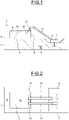
- an electronic device 1 comprises a support plate 2 and an electronic chip 3, including integrated circuits, of which a rear face 4 is fixed on a front face 5 of the support plate 2, via a layer of glue (not shown).
- the support plate 2 is made of a dielectric material and includes an integrated electrical connection network 6, at one or more metal levels, which comprises exposed front electrical connection pads 7 and 8 of the front face 5 and which are located laterally at distance from a side 9 of the electronic chip 3 and close to one of the other.
- the electronic chip 3 comprises exposed front electrical connection pads 10 and 11 of a front face 12 of this electronic chip 3, opposite its rear face 4, and which are located at a distance from the flank 9 of the electronic chip 3, not away from the front studs 7 and 8 of the support plate 2.
- a bare electrical connection wire 13 is placed between the exposed electrical connection pads 7 and 10 and electrical junctions 14 and 15 are produced by soldering respectively between the ends of the electrical connection wire 13 and the pads 7 and 10 and, on the other hand, a complementary electrical connection wire 16 is placed between the complementary uncovered electrical connection pads 8 and 11 and electrical junctions are produced by welding respectively between the end portions of the electrical connection 16 and pads 8 and 11. Electrical connection wires 13 and 16 are adjacent but distant from each other.
- This operation of placing the electrical connection wires 13 and 16 can be carried out using a suitable laying and welding machine, well known by the English term “wire bonding”.
- a determined quantity of an adherent liquid dielectric material is locally distributed above the electrical wire 13, so that this dielectric material completely surrounds the electrical connection wire 13 and completely covers the pads 7 and 10 and the junctions 14 and 15 After curing, this dielectric material forms a local dielectric coating 17.
- This operation is carried out using a suitable tool comprising a controlled dispensing syringe 18, capable of delivering at least one calibrated drop of the liquid dielectric material above the electrical connection wire 13, this dielectric material liquid flowing to ultimately surround the electrical connection wire 12 and cover the pads 7 and 10 and the junctions 14 and 15, in particular by capillarity or wetting effect.
- a suitable tool comprising a controlled dispensing syringe 18, capable of delivering at least one calibrated drop of the liquid dielectric material above the electrical connection wire 13, this dielectric material liquid flowing to ultimately surround the electrical connection wire 12 and cover the pads 7 and 10 and the junctions 14 and 15, in particular by capillarity or wetting effect.
- the liquid dielectric material is hardened to form the dielectric coating 17, either thanks to its intrinsic qualities of hardening at room temperature or hardening under the effect of a source of heat or light radiation.
- the dielectric material can be a suitable epoxy resin.
- a determined quantity of an adherent electrically conductive liquid material is locally distributed above the dielectric coating 17 and possibly the electrical connection wire 16, so that this conductive material completely surrounds the dielectric coating 17 and either in contact with the electrical connection wire 16 and/or the pads 8 and 11, this conductive material possibly overflowing on the front faces 5 and 12 of the support plate 2 and of the electronic chip 3.
- this conductive material produces a local electrically conductive shield 19 as close as possible to the electrical connection wire 13 and connected to the electrical connection wire 16 and to the pads 8 and 11.
- This operation is carried out using a suitable controlled tool comprising a controlled dispensing syringe 20, capable of delivering at least one calibrated drop of the liquid conductive material, this liquid conductive material flowing in particular by capillarity or wetting.
- a suitable controlled tool comprising a controlled dispensing syringe 20, capable of delivering at least one calibrated drop of the liquid conductive material, this liquid conductive material flowing in particular by capillarity or wetting.
- the liquid conductive material is hardened to form the local conductive shielding 19, thanks to its intrinsic qualities of hardening at room temperature or hardening under the effect of a source of heat or light radiation.
- the conductive material can be an epoxy resin filled with metallic particles.
- the final electronic device 1 is then obtained.
- the electrical connection wire 13 is intended for transporting electrical signals between the pads 7 and 10 of the support plate 2 and of the electronic chip 3.
- the conductive shield 19 constitutes electromagnetic protection of these electrical signals.
- the pads 8 and 11, connected by the electrical connection wire 16, constitute ground pads of the electrical circuits of the electronic device 1.
- the conductive shield 19, which is connected to the pads 8 and 11 and to the electrical connection wire 16 is connected to the ground of the electrical circuits of the electronic device 1.
- the electrical connection wire 16 could be eliminated.
- the electronic device 1 can comprise other electrical connection wires 13 connecting other pads 7 and 10 of the support plate 2 and of the electronic chip 3 and other electrical connection wires 16 connecting other pads 8 and 11 of the support plate 2 and of the electronic chip 3, also equipped with local dielectric coatings 17 and local conductive shields 19, the production steps of which would respectively be common.
- the support plate 2 could comprise a metal grid comprising a platform on which the electronic chip 3 would be mounted, the electrical connection wires 13 and 16 connecting the electronic chip 3 to the peripheral tabs of this grid.
Landscapes
- Shielding Devices Or Components To Electric Or Magnetic Fields (AREA)
Description
- La présente invention concerne le domaine des dispositifs électroniques et plus particulièrement ceux qui comprennent des puces électroniques montées sur des plaques de support, incluant des réseaux de connexion électrique ou des grilles de connexion électrique, et des fils de connexion électrique qui relient les puces aux plaques de support.
- Le document
JP H06 268100 - Le document
US 2010/0025864 décrit une structure ayant des plots de masse et des plots de signal couplés à des fils de soudage, et disposée sur un composant. Un premier revêtement isole au moins les plots de signal en laissant au moins les plots de masse dégagés. Un second revêtement entoure le premier revêtement et est électriquement couplé aux plots de masse. - Le document
JP2000 058579 - Dans le cas où des fils de connexion électrique transportent des signaux notamment à des fréquences élevées, ces signaux peuvent être atténués ou peuvent être perturbés par des champs électromagnétiques environnants et/ou émettent des champs électromagnétiques qui peuvent perturber l'environnement.
- A l'heure actuelle, pour réduire cette difficulté, il est proposé d'adjoindre aux dispositifs électroniques des plaques métalliques de blindage, éventuellement reliées à une masse. Néanmoins, la mise en place et la connexion électrique à une masse de telles plaques métalliques de blindage, combinées avec la réalisation de blocs d'encapsulation ou à la mise en place de couvercles d'encapsulation, posent des difficultés et sont onéreuses. De plus, comme les blindages obtenus sont globaux et à distance des fils de connexion électrique, la protection électromagnétique obtenue reste insuffisante.
- Différents aspects de l'invention sont définis dans les revendications annexées.
- Selon un mode de réalisation, il est proposé un procédé de réalisation d'une connexion électrique entre une puce électronique et une plaque de support sur laquelle cette puce est montée, le procédé étant selon la revendication 1.
- Le procédé peut en outre comprendre les étapes suivantes :
- mettre en place un fil complémentaire de connexion électrique entre un plot découvert de connexion électrique de la puce électronique et un plot découvert de connexion électrique de la plaque de support et réaliser des jonctions électriques entre les extrémités de ce fil complémentaire et ces plots, et
- réaliser le blindage local conducteur de sorte que ce blindage local conducteur soit en contact avec ce fil complémentaire de connexion électrique et/ou avec au moins l'un de ces plots de connexion électrique.
- Un mode de fabrication va maintenant être décrit à titre d'exemple non limitatif, illustré par le dessin annexé dans lequel :
- la
figure 1 représente une vue en coupe d'un dispositif électronique en cours de fabrication, selon une étape de fabrication ; - la
figure 2 représente une vue de dessus du dispositif électronique de lafigure 1 ; - la
figure 3 représente une vue en coupe du dispositif électronique en cours de fabrication, selon une étape ultérieure de fabrication ; - la
figure 4 représente une vue de dessus du dispositif électronique de lafigure 3 ; - la
figure 5 représente une vue en coupe du dispositif électronique en cours de fabrication, selon une étape ultérieure de fabrication, montrant le dispositif électronique obtenu ; et - la
figure 6 représente une vue de dessus du dispositif électronique de lafigure 5 . - Comme illustré sur les figures, un dispositif électronique 1 comprend une plaque de support 2 et une puce électronique 3, incluant des circuits intégrés, dont une face arrière 4 est fixée sur une face avant 5 de la plaque de support 2, par l'intermédiaire d'une couche de colle (non représentée).
- La plaque de support 2 est en une matière diélectrique et inclut un réseau intégré de connexion électrique 6, à un ou plusieurs niveaux métalliques, qui comprend des plots avant découverts de connexion électrique 7 et 8 de la face avant 5 et qui sont situés latéralement à distance d'un flanc 9 de la puce électronique 3 et à proximité l'un de l'autre.
- La puce électronique 3 comprend des plots avant découverts de connexion électrique 10 et 11 d'une face avant 12 de cette puce électronique 3, opposée à sa face arrière 4, et qui sont situés à distance du flanc 9 de la puce électronique 3, non loin des plots avant 7 et 8 de la plaque de support 2.
- On va maintenant décrire des étapes en vue de réaliser des connexions électriques entre les plots 7 et 10 et, optionnellement, les plots 8 et 11, respectivement de la plaque de support 2 et de la puce électronique 3.
- Selon une étape illustrée sur les
figures 1 et 2 , d'une part on met en place un fil nu de connexion électrique 13 entre les plots découverts de connexion électrique 7 et 10 et on réalise par soudure des jonctions électriques 14 et 15 respectivement entre les extrémités du fil de connexion électrique 13 et les plots 7 et 10 et, d'autre part, on met en place un fil complémentaire de connexion électrique 16 entre les plots complémentaires découverts de connexion électrique 8 et 11 et on réalise par soudure des jonctions électriques respectivement entre les portions d'extrémité du fil de connexion électrique 16 et les plots 8 et 11. Les fils de connexion électrique 13 et 16 sont voisins mais distants l'un de l'autre. - Cette opération de mise en place des fils de connexion électrique 13 et 16 peut être réalisée à l'aide d'une machine adaptée de pose et de soudage, bien connue sous le vocable anglais de « wire bonding ».
- Selon une étape ultérieure illustrée sur les
figures 3 et 4 , on distribue localement une quantité déterminée d'une matière diélectrique liquide adhérente au-dessus du fil électrique 13, de sorte que cette matière diélectrique entoure complètement le fil de connexion électrique 13 et recouvre complètement les plots 7 et 10 et les jonctions 14 et 15. Après durcissement, cette matière diélectrique réalise un enrobage diélectrique local 17. - Cette opération est réalisée à l'aide d'un outil adapté comprenant une seringue 18 de distribution contrôlée, apte à délivrer au moins une goutte calibrée de la matière diélectrique liquide au-dessus du fil de connexion électrique 13, cette matière diélectrique liquide s'écoulant pour en fin de compte entourer le fil de connexion électrique 12 et recouvrir les plots 7 et 10 et les jonctions 14 et 15, notamment par effet de capillarité ou de mouillage.
- Puis, la matière diélectrique liquide est durcie pour constituer l'enrobage diélectrique 17, soit grâce à ses qualités intrinsèques de durcissement à la température ambiante ou de durcissement sous l'effet d'une source de chaleur ou de rayonnement lumineux. Par exemple, la matière diélectrique peut être une résine époxy adaptée.
- Selon une étape ultérieure illustrée sur les
figures 5 et 6 , on distribue localement une quantité déterminée d'une matière liquide adhérente conductrice de l'électricité au-dessus de l'enrobage diélectrique 17 et éventuellement du fil de connexion électrique 16, de sorte que cette matière conductrice entoure complètement l'enrobage diélectrique 17 et soit en contact avec le fil de connexion électrique 16 et/ou les plots 8 et 11, cette matière conductrice débordant éventuellement sur les faces avant 5 et 12 de la plaque de support 2 et de la puce électronique 3. Après durcissement, cette matière conductrice réalise un blindage local conducteur de l'électricité 19 au plus près du fil de connexion électrique 13 et relié au fil de connexion électrique 16 et aux plots 8 et 11. - Cette opération est réalisée à l'aide d'un outil contrôlé adapté comprenant une seringue 20 de distribution contrôlée, apte à délivrer au moins une goutte calibrée de la matière conductrice liquide, cette matière conductrice liquide s'écoulant notamment par effet de capillarité ou de mouillage.
- Puis, la matière conductrice liquide est durcie pour constituer le blindage local conducteur 19, grâce à ses qualités intrinsèques de durcissement à la température ambiante ou de durcissement sous l'effet d'une source de chaleur ou de rayonnement lumineux. Par exemple, la matière conductrice peut être une résine époxy chargée de particules métalliques.
- Le dispositif électronique 1 final est alors obtenu.
- Le fil de connexion électrique 13 est destiné au transport de signaux électriques entre les plots 7 et 10 de la plaque de support 2 et de la puce électronique 3. Le blindage conducteur 19 constitue une protection électromagnétique de ces signaux électriques.
- Les plots 8 et 11, reliés par le fil de connexion électrique 16, constituent des plots de masse des circuits électriques du dispositif électronique 1. Ainsi, le blindage conducteur 19, qui est relié aux plots 8 et 11 et au fil de connexion électrique 16, est relié à la masse des circuits électriques du dispositif électronique 1.
- Selon une variante de réalisation, le fil de connexion électrique 16 pourrait être supprimé.
- Bien entendu, le dispositif électronique 1 peut comprendre d'autres fils de connexion électrique 13 reliant d'autres plots 7 et 10 de la plaque de support 2 et de la puce électronique 3 et d'autres fils de connexion électrique 16 reliant d'autres plots 8 et 11 de la plaque de support 2 et de la puce électronique 3, également équipés d'enrobages diélectriques locaux 17 et de blindages conducteurs locaux 19, dont les étapes de réalisation seraient respectivement communes.
- Selon une variante de réalisation, la plaque de support 2 pourrait comprendre une grille métallique comprenant une plateforme sur laquelle serait montée la puce électronique 3, les fils de connexion électrique 13 et 16 reliant la puce électronique 3 à des pattes périphériques de cette grille.
Claims (2)
- Procédé de réalisation d'une connexion électrique entre une puce électronique (3) et une plaque de support (2) sur laquelle cette puce est montée, comprenant les étapes suivantes :mettre en place un fil de connexion électrique (13) entre un plot découvert de connexion électrique (10) de la puce électronique et un plot découvert de connexion électrique (7)de la plaque de support et réaliser des jonctions électriques (14,15) entre les extrémités du fil et les plots,réaliser un enrobage local diélectrique (17) en une matière diélectrique, qui entoure le fil de connexion électrique (13) et recouvre les plots (7,10) et les jonctions, par distribution locale d'une quantité déterminée de la matière diélectrique à l'état liquide, sous la forme d'une goutte calibrée qui s'écoule par effet de capillarité ou de mouillage, à l'aide d'un outil contrôlé comprenant une seringue de distribution contrôlée (18), et durcissement de cette matière diélectrique, etréaliser un blindage local conducteur (19) en une matière conductrice de l'électricité, qui recouvre ledit enrobage local diélectrique, par distribution locale d'une quantité déterminée d'une matière conductrice de l'électricité à l'état liquide, sous la forme d'une goutte calibrée qui s'écoule par effet de capillarité ou de mouillage, à l'aide d'un outil contrôlé comprenant une seringue de distribution contrôlée (20), et durcissement de cette matière conductrice.
- Procédé selon la revendication 1, comprenant les étapes suivantes :mettre en place un fil complémentaire de connexion électrique (16) entre un plot découvert de connexion électrique (11) de la puce électronique et un plot découvert de connexion électrique (8) de la plaque de support et réaliser des jonctions électriques entre les extrémités de ce fil complémentaire et ces plots, etréaliser le blindage local conducteur (19) de sorte que ce blindage local conducteur (19) soit en contact avec ce fil complémentaire de connexion électrique (16) et/ou avec au moins l'un de ces plots de connexion électrique.
Applications Claiming Priority (1)
| Application Number | Priority Date | Filing Date | Title |
|---|---|---|---|
| FR1660624A FR3058261A1 (fr) | 2016-11-03 | 2016-11-03 | Procede de realisation d'une connexion electrique entre une puce electronique et une plaque de support et dispositif electronique |
Publications (2)
| Publication Number | Publication Date |
|---|---|
| EP3319114A1 EP3319114A1 (fr) | 2018-05-09 |
| EP3319114B1 true EP3319114B1 (fr) | 2022-06-29 |
Family
ID=58213196
Family Applications (1)
| Application Number | Title | Priority Date | Filing Date |
|---|---|---|---|
| EP17168179.4A Active EP3319114B1 (fr) | 2016-11-03 | 2017-04-26 | Procédé de réalisation d'une connexion électrique entre une puce électronique et une plaque de support et dispositif électronique |
Country Status (3)
| Country | Link |
|---|---|
| EP (1) | EP3319114B1 (fr) |
| CN (2) | CN206877989U (fr) |
| FR (1) | FR3058261A1 (fr) |
Families Citing this family (2)
| Publication number | Priority date | Publication date | Assignee | Title |
|---|---|---|---|---|
| FR3058261A1 (fr) * | 2016-11-03 | 2018-05-04 | Stmicroelectronics (Grenoble 2) Sas | Procede de realisation d'une connexion electrique entre une puce electronique et une plaque de support et dispositif electronique |
| US10224306B2 (en) | 2016-11-03 | 2019-03-05 | Stmicroelectronics (Grenoble 2) Sas | Method for forming an electrical connection between an electronic chip and a carrier substrate and electronic device |
Family Cites Families (10)
| Publication number | Priority date | Publication date | Assignee | Title |
|---|---|---|---|---|
| DE2514011C2 (de) * | 1975-03-29 | 1983-10-27 | Licentia Patent-Verwaltungs-Gmbh, 6000 Frankfurt | Gehäuse für ein Halbleiterelement |
| JP2689467B2 (ja) * | 1988-03-29 | 1997-12-10 | 日本電気株式会社 | 半導体集積回路装置のパッケージ |
| JPH06268100A (ja) * | 1993-03-12 | 1994-09-22 | Nippon Telegr & Teleph Corp <Ntt> | 半導体装置の封止構造および封止方法 |
| JP2000058579A (ja) * | 1998-08-04 | 2000-02-25 | Hitachi Ltd | 半導体装置およびその製造方法 |
| JP2002064166A (ja) * | 2000-06-06 | 2002-02-28 | Nippon Steel Corp | 半導体装置およびその製造方法、ならびに半導体装置の樹脂封止装置 |
| US20040070065A1 (en) * | 2002-10-11 | 2004-04-15 | Aritharan Thurairajaratnam | Controlled impedance for wire bonding interconnects |
| KR100575086B1 (ko) * | 2004-11-11 | 2006-05-03 | 삼성전자주식회사 | 도전성 몰딩 컴파운드를 구비한 반도체 패키지 및 그제조방법 |
| US20100025864A1 (en) * | 2008-07-31 | 2010-02-04 | International Business Machines Corporation | Shielded wirebond |
| KR100950511B1 (ko) * | 2009-09-22 | 2010-03-30 | 테세라 리써치 엘엘씨 | 와이어 본딩 및 도전성 기준 소자에 의해 제어되는 임피던스를 포함하는 마이크로전자 어셈블리 |
| FR3058261A1 (fr) * | 2016-11-03 | 2018-05-04 | Stmicroelectronics (Grenoble 2) Sas | Procede de realisation d'une connexion electrique entre une puce electronique et une plaque de support et dispositif electronique |
-
2016
- 2016-11-03 FR FR1660624A patent/FR3058261A1/fr not_active Ceased
-
2017
- 2017-04-26 EP EP17168179.4A patent/EP3319114B1/fr active Active
- 2017-05-24 CN CN201720588097.1U patent/CN206877989U/zh active Active
- 2017-05-24 CN CN201710374185.6A patent/CN108022910A/zh active Pending
Also Published As
| Publication number | Publication date |
|---|---|
| FR3058261A1 (fr) | 2018-05-04 |
| CN206877989U (zh) | 2018-01-12 |
| EP3319114A1 (fr) | 2018-05-09 |
| CN108022910A (zh) | 2018-05-11 |
Similar Documents
| Publication | Publication Date | Title |
|---|---|---|
| US10192835B2 (en) | Substrate designed to provide EMI shielding | |
| US20220102166A1 (en) | Leadframe package with pre-applied filler material | |
| CN104851851B (zh) | 半导体装置及其制造方法 | |
| US20250070081A1 (en) | Method for forming an electrical connection between an electronic chip and a carrier substrate and electronic device | |
| US7374969B2 (en) | Semiconductor package with conductive molding compound and manufacturing method thereof | |
| JPWO2017043621A1 (ja) | 高周波モジュール | |
| FR3040534A1 (fr) | Dispositif electronique muni d'une couche conductrice et procede de fabrication | |
| WO2018207583A1 (fr) | Dispositif à semi-conducteur et son procédé de fabrication | |
| EP3319115B1 (fr) | Procédé de réalisation d'une connexion électrique entre une puce électronique et une plaque de support et dispositif électronique | |
| EP3319116B1 (fr) | Procédé de réalisation d'une connexion électrique entre une puce électronique et une plaque de support et dispositif électronique | |
| EP3319114A1 (fr) | Procédé de réalisation d'une connexion électrique entre une puce électronique et une plaque de support et dispositif électronique | |
| WO2018091852A1 (fr) | Circuit intégré forme de deux puces connectées en série | |
| US6271607B1 (en) | Sub-assemblies with electronic components, for motor vehicle alternators | |
| FR2968126A1 (fr) | Boitier semi-conducteur a via thermique et procédé de fabrication | |
| KR100788858B1 (ko) | 집적 회로 패키지의 구조물 및 어셈블리 방법 | |
| FR3041859A1 (fr) | Dispositif electronique muni d'un fil conducteur integre et procede de fabrication | |
| TWI915000B (zh) | 一種半導體封裝結構的製造方法及半導體封裝結構 | |
| US20180123007A1 (en) | Radiation-Emitting Semiconductor Component and Production Method of a Plurality of Semiconductor Components | |
| US20130264714A1 (en) | Semiconductor device and method of assembling same | |
| CN120977880A (zh) | 制造具有可润湿侧翼的电子部件的方法 | |
| CN116093039A (zh) | 一种芯片封装结构及封装方法 | |
| FR3103316A1 (fr) | Cadre métallique conducteur pour module électronique de puissance et procédé de fabrication associé | |
| FR2670987A1 (fr) | Procede de realisation d'au moins une traversee conductrice a travers un trou traversant d'un substrat isolant. | |
| TW201505213A (zh) | 光電組件及光電組件的製備方法 | |
| WO2000068991A1 (fr) | Boitier pbga a grille de billage integree |
Legal Events
| Date | Code | Title | Description |
|---|---|---|---|
| PUAI | Public reference made under article 153(3) epc to a published international application that has entered the european phase |
Free format text: ORIGINAL CODE: 0009012 |
|
| STAA | Information on the status of an ep patent application or granted ep patent |
Free format text: STATUS: REQUEST FOR EXAMINATION WAS MADE |
|
| 17P | Request for examination filed |
Effective date: 20170426 |
|
| AK | Designated contracting states |
Kind code of ref document: A1 Designated state(s): AL AT BE BG CH CY CZ DE DK EE ES FI FR GB GR HR HU IE IS IT LI LT LU LV MC MK MT NL NO PL PT RO RS SE SI SK SM TR |
|
| AX | Request for extension of the european patent |
Extension state: BA ME |
|
| STAA | Information on the status of an ep patent application or granted ep patent |
Free format text: STATUS: EXAMINATION IS IN PROGRESS |
|
| 17Q | First examination report despatched |
Effective date: 20210319 |
|
| GRAP | Despatch of communication of intention to grant a patent |
Free format text: ORIGINAL CODE: EPIDOSNIGR1 |
|
| STAA | Information on the status of an ep patent application or granted ep patent |
Free format text: STATUS: GRANT OF PATENT IS INTENDED |
|
| RIC1 | Information provided on ipc code assigned before grant |
Ipc: H01L 23/00 20060101ALI20220125BHEP Ipc: H01L 21/56 20060101ALI20220125BHEP Ipc: H01L 23/31 20060101ALI20220125BHEP Ipc: H01L 23/66 20060101ALI20220125BHEP Ipc: H01L 23/552 20060101ALI20220125BHEP Ipc: H01L 23/49 20060101ALI20220125BHEP Ipc: H01L 21/60 20060101AFI20220125BHEP |
|
| INTG | Intention to grant announced |
Effective date: 20220209 |
|
| GRAS | Grant fee paid |
Free format text: ORIGINAL CODE: EPIDOSNIGR3 |
|
| GRAA | (expected) grant |
Free format text: ORIGINAL CODE: 0009210 |
|
| STAA | Information on the status of an ep patent application or granted ep patent |
Free format text: STATUS: THE PATENT HAS BEEN GRANTED |
|
| AK | Designated contracting states |
Kind code of ref document: B1 Designated state(s): AL AT BE BG CH CY CZ DE DK EE ES FI FR GB GR HR HU IE IS IT LI LT LU LV MC MK MT NL NO PL PT RO RS SE SI SK SM TR |
|
| REG | Reference to a national code |
Ref country code: CH Ref legal event code: EP |
|
| REG | Reference to a national code |
Ref country code: AT Ref legal event code: REF Ref document number: 1501878 Country of ref document: AT Kind code of ref document: T Effective date: 20220715 |
|
| REG | Reference to a national code |
Ref country code: IE Ref legal event code: FG4D Free format text: LANGUAGE OF EP DOCUMENT: FRENCH |
|
| REG | Reference to a national code |
Ref country code: DE Ref legal event code: R096 Ref document number: 602017058935 Country of ref document: DE |
|
| REG | Reference to a national code |
Ref country code: LT Ref legal event code: MG9D |
|
| PG25 | Lapsed in a contracting state [announced via postgrant information from national office to epo] |
Ref country code: SE Free format text: LAPSE BECAUSE OF FAILURE TO SUBMIT A TRANSLATION OF THE DESCRIPTION OR TO PAY THE FEE WITHIN THE PRESCRIBED TIME-LIMIT Effective date: 20220629 Ref country code: NO Free format text: LAPSE BECAUSE OF FAILURE TO SUBMIT A TRANSLATION OF THE DESCRIPTION OR TO PAY THE FEE WITHIN THE PRESCRIBED TIME-LIMIT Effective date: 20220929 Ref country code: LT Free format text: LAPSE BECAUSE OF FAILURE TO SUBMIT A TRANSLATION OF THE DESCRIPTION OR TO PAY THE FEE WITHIN THE PRESCRIBED TIME-LIMIT Effective date: 20220629 Ref country code: HR Free format text: LAPSE BECAUSE OF FAILURE TO SUBMIT A TRANSLATION OF THE DESCRIPTION OR TO PAY THE FEE WITHIN THE PRESCRIBED TIME-LIMIT Effective date: 20220629 Ref country code: GR Free format text: LAPSE BECAUSE OF FAILURE TO SUBMIT A TRANSLATION OF THE DESCRIPTION OR TO PAY THE FEE WITHIN THE PRESCRIBED TIME-LIMIT Effective date: 20220930 Ref country code: FI Free format text: LAPSE BECAUSE OF FAILURE TO SUBMIT A TRANSLATION OF THE DESCRIPTION OR TO PAY THE FEE WITHIN THE PRESCRIBED TIME-LIMIT Effective date: 20220629 Ref country code: BG Free format text: LAPSE BECAUSE OF FAILURE TO SUBMIT A TRANSLATION OF THE DESCRIPTION OR TO PAY THE FEE WITHIN THE PRESCRIBED TIME-LIMIT Effective date: 20220929 |
|
| REG | Reference to a national code |
Ref country code: NL Ref legal event code: MP Effective date: 20220629 |
|
| REG | Reference to a national code |
Ref country code: AT Ref legal event code: MK05 Ref document number: 1501878 Country of ref document: AT Kind code of ref document: T Effective date: 20220629 |
|
| PG25 | Lapsed in a contracting state [announced via postgrant information from national office to epo] |
Ref country code: RS Free format text: LAPSE BECAUSE OF FAILURE TO SUBMIT A TRANSLATION OF THE DESCRIPTION OR TO PAY THE FEE WITHIN THE PRESCRIBED TIME-LIMIT Effective date: 20220629 Ref country code: LV Free format text: LAPSE BECAUSE OF FAILURE TO SUBMIT A TRANSLATION OF THE DESCRIPTION OR TO PAY THE FEE WITHIN THE PRESCRIBED TIME-LIMIT Effective date: 20220629 |
|
| PG25 | Lapsed in a contracting state [announced via postgrant information from national office to epo] |
Ref country code: NL Free format text: LAPSE BECAUSE OF FAILURE TO SUBMIT A TRANSLATION OF THE DESCRIPTION OR TO PAY THE FEE WITHIN THE PRESCRIBED TIME-LIMIT Effective date: 20220629 |
|
| PG25 | Lapsed in a contracting state [announced via postgrant information from national office to epo] |
Ref country code: SM Free format text: LAPSE BECAUSE OF FAILURE TO SUBMIT A TRANSLATION OF THE DESCRIPTION OR TO PAY THE FEE WITHIN THE PRESCRIBED TIME-LIMIT Effective date: 20220629 Ref country code: SK Free format text: LAPSE BECAUSE OF FAILURE TO SUBMIT A TRANSLATION OF THE DESCRIPTION OR TO PAY THE FEE WITHIN THE PRESCRIBED TIME-LIMIT Effective date: 20220629 Ref country code: RO Free format text: LAPSE BECAUSE OF FAILURE TO SUBMIT A TRANSLATION OF THE DESCRIPTION OR TO PAY THE FEE WITHIN THE PRESCRIBED TIME-LIMIT Effective date: 20220629 Ref country code: PT Free format text: LAPSE BECAUSE OF FAILURE TO SUBMIT A TRANSLATION OF THE DESCRIPTION OR TO PAY THE FEE WITHIN THE PRESCRIBED TIME-LIMIT Effective date: 20221031 Ref country code: ES Free format text: LAPSE BECAUSE OF FAILURE TO SUBMIT A TRANSLATION OF THE DESCRIPTION OR TO PAY THE FEE WITHIN THE PRESCRIBED TIME-LIMIT Effective date: 20220629 Ref country code: EE Free format text: LAPSE BECAUSE OF FAILURE TO SUBMIT A TRANSLATION OF THE DESCRIPTION OR TO PAY THE FEE WITHIN THE PRESCRIBED TIME-LIMIT Effective date: 20220629 Ref country code: AT Free format text: LAPSE BECAUSE OF FAILURE TO SUBMIT A TRANSLATION OF THE DESCRIPTION OR TO PAY THE FEE WITHIN THE PRESCRIBED TIME-LIMIT Effective date: 20220629 |
|
| PG25 | Lapsed in a contracting state [announced via postgrant information from national office to epo] |
Ref country code: PL Free format text: LAPSE BECAUSE OF FAILURE TO SUBMIT A TRANSLATION OF THE DESCRIPTION OR TO PAY THE FEE WITHIN THE PRESCRIBED TIME-LIMIT Effective date: 20220629 Ref country code: IS Free format text: LAPSE BECAUSE OF FAILURE TO SUBMIT A TRANSLATION OF THE DESCRIPTION OR TO PAY THE FEE WITHIN THE PRESCRIBED TIME-LIMIT Effective date: 20221029 |
|
| REG | Reference to a national code |
Ref country code: DE Ref legal event code: R097 Ref document number: 602017058935 Country of ref document: DE |
|
| PG25 | Lapsed in a contracting state [announced via postgrant information from national office to epo] |
Ref country code: AL Free format text: LAPSE BECAUSE OF FAILURE TO SUBMIT A TRANSLATION OF THE DESCRIPTION OR TO PAY THE FEE WITHIN THE PRESCRIBED TIME-LIMIT Effective date: 20220629 |
|
| PG25 | Lapsed in a contracting state [announced via postgrant information from national office to epo] |
Ref country code: DK Free format text: LAPSE BECAUSE OF FAILURE TO SUBMIT A TRANSLATION OF THE DESCRIPTION OR TO PAY THE FEE WITHIN THE PRESCRIBED TIME-LIMIT Effective date: 20220629 Ref country code: CZ Free format text: LAPSE BECAUSE OF FAILURE TO SUBMIT A TRANSLATION OF THE DESCRIPTION OR TO PAY THE FEE WITHIN THE PRESCRIBED TIME-LIMIT Effective date: 20220629 |
|
| PLBE | No opposition filed within time limit |
Free format text: ORIGINAL CODE: 0009261 |
|
| STAA | Information on the status of an ep patent application or granted ep patent |
Free format text: STATUS: NO OPPOSITION FILED WITHIN TIME LIMIT |
|
| 26N | No opposition filed |
Effective date: 20230330 |
|
| PG25 | Lapsed in a contracting state [announced via postgrant information from national office to epo] |
Ref country code: SI Free format text: LAPSE BECAUSE OF FAILURE TO SUBMIT A TRANSLATION OF THE DESCRIPTION OR TO PAY THE FEE WITHIN THE PRESCRIBED TIME-LIMIT Effective date: 20220629 |
|
| REG | Reference to a national code |
Ref country code: CH Ref legal event code: PL |
|
| GBPC | Gb: european patent ceased through non-payment of renewal fee |
Effective date: 20230426 |
|
| PG25 | Lapsed in a contracting state [announced via postgrant information from national office to epo] |
Ref country code: LU Free format text: LAPSE BECAUSE OF NON-PAYMENT OF DUE FEES Effective date: 20230426 |
|
| REG | Reference to a national code |
Ref country code: BE Ref legal event code: MM Effective date: 20230430 |
|
| PG25 | Lapsed in a contracting state [announced via postgrant information from national office to epo] |
Ref country code: MC Free format text: LAPSE BECAUSE OF FAILURE TO SUBMIT A TRANSLATION OF THE DESCRIPTION OR TO PAY THE FEE WITHIN THE PRESCRIBED TIME-LIMIT Effective date: 20220629 |
|
| PG25 | Lapsed in a contracting state [announced via postgrant information from national office to epo] |
Ref country code: GB Free format text: LAPSE BECAUSE OF NON-PAYMENT OF DUE FEES Effective date: 20230426 |
|
| PG25 | Lapsed in a contracting state [announced via postgrant information from national office to epo] |
Ref country code: MC Free format text: LAPSE BECAUSE OF FAILURE TO SUBMIT A TRANSLATION OF THE DESCRIPTION OR TO PAY THE FEE WITHIN THE PRESCRIBED TIME-LIMIT Effective date: 20220629 Ref country code: LI Free format text: LAPSE BECAUSE OF NON-PAYMENT OF DUE FEES Effective date: 20230430 Ref country code: IT Free format text: LAPSE BECAUSE OF FAILURE TO SUBMIT A TRANSLATION OF THE DESCRIPTION OR TO PAY THE FEE WITHIN THE PRESCRIBED TIME-LIMIT Effective date: 20220629 Ref country code: GB Free format text: LAPSE BECAUSE OF NON-PAYMENT OF DUE FEES Effective date: 20230426 Ref country code: FR Free format text: LAPSE BECAUSE OF NON-PAYMENT OF DUE FEES Effective date: 20230430 Ref country code: CH Free format text: LAPSE BECAUSE OF NON-PAYMENT OF DUE FEES Effective date: 20230430 |
|
| REG | Reference to a national code |
Ref country code: IE Ref legal event code: MM4A |
|
| PG25 | Lapsed in a contracting state [announced via postgrant information from national office to epo] |
Ref country code: BE Free format text: LAPSE BECAUSE OF NON-PAYMENT OF DUE FEES Effective date: 20230430 |
|
| PG25 | Lapsed in a contracting state [announced via postgrant information from national office to epo] |
Ref country code: IE Free format text: LAPSE BECAUSE OF NON-PAYMENT OF DUE FEES Effective date: 20230426 |
|
| PG25 | Lapsed in a contracting state [announced via postgrant information from national office to epo] |
Ref country code: IE Free format text: LAPSE BECAUSE OF NON-PAYMENT OF DUE FEES Effective date: 20230426 |
|
| PG25 | Lapsed in a contracting state [announced via postgrant information from national office to epo] |
Ref country code: BG Free format text: LAPSE BECAUSE OF FAILURE TO SUBMIT A TRANSLATION OF THE DESCRIPTION OR TO PAY THE FEE WITHIN THE PRESCRIBED TIME-LIMIT Effective date: 20220629 |
|
| PG25 | Lapsed in a contracting state [announced via postgrant information from national office to epo] |
Ref country code: BG Free format text: LAPSE BECAUSE OF FAILURE TO SUBMIT A TRANSLATION OF THE DESCRIPTION OR TO PAY THE FEE WITHIN THE PRESCRIBED TIME-LIMIT Effective date: 20220629 |
|
| PGFP | Annual fee paid to national office [announced via postgrant information from national office to epo] |
Ref country code: DE Payment date: 20250319 Year of fee payment: 9 |
|
| PG25 | Lapsed in a contracting state [announced via postgrant information from national office to epo] |
Ref country code: CY Free format text: LAPSE BECAUSE OF FAILURE TO SUBMIT A TRANSLATION OF THE DESCRIPTION OR TO PAY THE FEE WITHIN THE PRESCRIBED TIME-LIMIT; INVALID AB INITIO Effective date: 20170426 |
|
| PG25 | Lapsed in a contracting state [announced via postgrant information from national office to epo] |
Ref country code: HU Free format text: LAPSE BECAUSE OF FAILURE TO SUBMIT A TRANSLATION OF THE DESCRIPTION OR TO PAY THE FEE WITHIN THE PRESCRIBED TIME-LIMIT; INVALID AB INITIO Effective date: 20170426 |
|
| REG | Reference to a national code |
Ref country code: DE Ref legal event code: R079 Ref document number: 602017058935 Country of ref document: DE Free format text: PREVIOUS MAIN CLASS: H01L0021600000 Ipc: H10W0070010000 |
|
| PG25 | Lapsed in a contracting state [announced via postgrant information from national office to epo] |
Ref country code: TR Free format text: LAPSE BECAUSE OF FAILURE TO SUBMIT A TRANSLATION OF THE DESCRIPTION OR TO PAY THE FEE WITHIN THE PRESCRIBED TIME-LIMIT Effective date: 20220629 |