EP3316470A1 - Inverter with charging capability - Google Patents
Inverter with charging capability Download PDFInfo
- Publication number
- EP3316470A1 EP3316470A1 EP15896291.0A EP15896291A EP3316470A1 EP 3316470 A1 EP3316470 A1 EP 3316470A1 EP 15896291 A EP15896291 A EP 15896291A EP 3316470 A1 EP3316470 A1 EP 3316470A1
- Authority
- EP
- European Patent Office
- Prior art keywords
- diode
- switching element
- phase
- inverter
- charging capability
- Prior art date
- Legal status (The legal status is an assumption and is not a legal conclusion. Google has not performed a legal analysis and makes no representation as to the accuracy of the status listed.)
- Granted
Links
- 239000003990 capacitor Substances 0.000 claims abstract description 34
- 230000000694 effects Effects 0.000 description 11
- 230000003071 parasitic effect Effects 0.000 description 7
- 230000002265 prevention Effects 0.000 description 5
- 230000007423 decrease Effects 0.000 description 4
- 230000004048 modification Effects 0.000 description 3
- 238000012986 modification Methods 0.000 description 3
- 239000004065 semiconductor Substances 0.000 description 3
- 230000000903 blocking effect Effects 0.000 description 2
- 238000000034 method Methods 0.000 description 2
- 230000006641 stabilisation Effects 0.000 description 2
- 238000011105 stabilization Methods 0.000 description 2
- 230000002411 adverse Effects 0.000 description 1
- 238000007796 conventional method Methods 0.000 description 1
- 230000005684 electric field Effects 0.000 description 1
- 230000000087 stabilizing effect Effects 0.000 description 1
- 239000000758 substrate Substances 0.000 description 1
- 230000001360 synchronised effect Effects 0.000 description 1
Images


Classifications
-
- H—ELECTRICITY
- H02—GENERATION; CONVERSION OR DISTRIBUTION OF ELECTRIC POWER
- H02M—APPARATUS FOR CONVERSION BETWEEN AC AND AC, BETWEEN AC AND DC, OR BETWEEN DC AND DC, AND FOR USE WITH MAINS OR SIMILAR POWER SUPPLY SYSTEMS; CONVERSION OF DC OR AC INPUT POWER INTO SURGE OUTPUT POWER; CONTROL OR REGULATION THEREOF
- H02M7/00—Conversion of ac power input into dc power output; Conversion of dc power input into ac power output
- H02M7/42—Conversion of dc power input into ac power output without possibility of reversal
- H02M7/44—Conversion of dc power input into ac power output without possibility of reversal by static converters
- H02M7/48—Conversion of dc power input into ac power output without possibility of reversal by static converters using discharge tubes with control electrode or semiconductor devices with control electrode
- H02M7/53—Conversion of dc power input into ac power output without possibility of reversal by static converters using discharge tubes with control electrode or semiconductor devices with control electrode using devices of a triode or transistor type requiring continuous application of a control signal
- H02M7/537—Conversion of dc power input into ac power output without possibility of reversal by static converters using discharge tubes with control electrode or semiconductor devices with control electrode using devices of a triode or transistor type requiring continuous application of a control signal using semiconductor devices only, e.g. single switched pulse inverters
- H02M7/5387—Conversion of dc power input into ac power output without possibility of reversal by static converters using discharge tubes with control electrode or semiconductor devices with control electrode using devices of a triode or transistor type requiring continuous application of a control signal using semiconductor devices only, e.g. single switched pulse inverters in a bridge configuration
- H02M7/53871—Conversion of dc power input into ac power output without possibility of reversal by static converters using discharge tubes with control electrode or semiconductor devices with control electrode using devices of a triode or transistor type requiring continuous application of a control signal using semiconductor devices only, e.g. single switched pulse inverters in a bridge configuration with automatic control of output voltage or current
-
- H—ELECTRICITY
- H02—GENERATION; CONVERSION OR DISTRIBUTION OF ELECTRIC POWER
- H02M—APPARATUS FOR CONVERSION BETWEEN AC AND AC, BETWEEN AC AND DC, OR BETWEEN DC AND DC, AND FOR USE WITH MAINS OR SIMILAR POWER SUPPLY SYSTEMS; CONVERSION OF DC OR AC INPUT POWER INTO SURGE OUTPUT POWER; CONTROL OR REGULATION THEREOF
- H02M1/00—Details of apparatus for conversion
- H02M1/0095—Hybrid converter topologies, e.g. NPC mixed with flying capacitor, thyristor converter mixed with MMC or charge pump mixed with buck
-
- B—PERFORMING OPERATIONS; TRANSPORTING
- B60—VEHICLES IN GENERAL
- B60L—PROPULSION OF ELECTRICALLY-PROPELLED VEHICLES; SUPPLYING ELECTRIC POWER FOR AUXILIARY EQUIPMENT OF ELECTRICALLY-PROPELLED VEHICLES; ELECTRODYNAMIC BRAKE SYSTEMS FOR VEHICLES IN GENERAL; MAGNETIC SUSPENSION OR LEVITATION FOR VEHICLES; MONITORING OPERATING VARIABLES OF ELECTRICALLY-PROPELLED VEHICLES; ELECTRIC SAFETY DEVICES FOR ELECTRICALLY-PROPELLED VEHICLES
- B60L50/00—Electric propulsion with power supplied within the vehicle
- B60L50/50—Electric propulsion with power supplied within the vehicle using propulsion power supplied by batteries or fuel cells
- B60L50/51—Electric propulsion with power supplied within the vehicle using propulsion power supplied by batteries or fuel cells characterised by AC-motors
-
- H—ELECTRICITY
- H02—GENERATION; CONVERSION OR DISTRIBUTION OF ELECTRIC POWER
- H02J—CIRCUIT ARRANGEMENTS OR SYSTEMS FOR SUPPLYING OR DISTRIBUTING ELECTRIC POWER; SYSTEMS FOR STORING ELECTRIC ENERGY
- H02J7/00—Circuit arrangements for charging or depolarising batteries or for supplying loads from batteries
-
- H—ELECTRICITY
- H02—GENERATION; CONVERSION OR DISTRIBUTION OF ELECTRIC POWER
- H02M—APPARATUS FOR CONVERSION BETWEEN AC AND AC, BETWEEN AC AND DC, OR BETWEEN DC AND DC, AND FOR USE WITH MAINS OR SIMILAR POWER SUPPLY SYSTEMS; CONVERSION OF DC OR AC INPUT POWER INTO SURGE OUTPUT POWER; CONTROL OR REGULATION THEREOF
- H02M1/00—Details of apparatus for conversion
- H02M1/08—Circuits specially adapted for the generation of control voltages for semiconductor devices incorporated in static converters
-
- H—ELECTRICITY
- H02—GENERATION; CONVERSION OR DISTRIBUTION OF ELECTRIC POWER
- H02M—APPARATUS FOR CONVERSION BETWEEN AC AND AC, BETWEEN AC AND DC, OR BETWEEN DC AND DC, AND FOR USE WITH MAINS OR SIMILAR POWER SUPPLY SYSTEMS; CONVERSION OF DC OR AC INPUT POWER INTO SURGE OUTPUT POWER; CONTROL OR REGULATION THEREOF
- H02M7/00—Conversion of ac power input into dc power output; Conversion of dc power input into ac power output
- H02M7/42—Conversion of dc power input into ac power output without possibility of reversal
- H02M7/44—Conversion of dc power input into ac power output without possibility of reversal by static converters
- H02M7/48—Conversion of dc power input into ac power output without possibility of reversal by static converters using discharge tubes with control electrode or semiconductor devices with control electrode
- H02M7/53—Conversion of dc power input into ac power output without possibility of reversal by static converters using discharge tubes with control electrode or semiconductor devices with control electrode using devices of a triode or transistor type requiring continuous application of a control signal
- H02M7/537—Conversion of dc power input into ac power output without possibility of reversal by static converters using discharge tubes with control electrode or semiconductor devices with control electrode using devices of a triode or transistor type requiring continuous application of a control signal using semiconductor devices only, e.g. single switched pulse inverters
- H02M7/5387—Conversion of dc power input into ac power output without possibility of reversal by static converters using discharge tubes with control electrode or semiconductor devices with control electrode using devices of a triode or transistor type requiring continuous application of a control signal using semiconductor devices only, e.g. single switched pulse inverters in a bridge configuration
-
- B—PERFORMING OPERATIONS; TRANSPORTING
- B60—VEHICLES IN GENERAL
- B60L—PROPULSION OF ELECTRICALLY-PROPELLED VEHICLES; SUPPLYING ELECTRIC POWER FOR AUXILIARY EQUIPMENT OF ELECTRICALLY-PROPELLED VEHICLES; ELECTRODYNAMIC BRAKE SYSTEMS FOR VEHICLES IN GENERAL; MAGNETIC SUSPENSION OR LEVITATION FOR VEHICLES; MONITORING OPERATING VARIABLES OF ELECTRICALLY-PROPELLED VEHICLES; ELECTRIC SAFETY DEVICES FOR ELECTRICALLY-PROPELLED VEHICLES
- B60L2210/00—Converter types
- B60L2210/40—DC to AC converters
-
- B—PERFORMING OPERATIONS; TRANSPORTING
- B60—VEHICLES IN GENERAL
- B60Y—INDEXING SCHEME RELATING TO ASPECTS CROSS-CUTTING VEHICLE TECHNOLOGY
- B60Y2200/00—Type of vehicle
- B60Y2200/90—Vehicles comprising electric prime movers
- B60Y2200/91—Electric vehicles
-
- B—PERFORMING OPERATIONS; TRANSPORTING
- B60—VEHICLES IN GENERAL
- B60Y—INDEXING SCHEME RELATING TO ASPECTS CROSS-CUTTING VEHICLE TECHNOLOGY
- B60Y2200/00—Type of vehicle
- B60Y2200/90—Vehicles comprising electric prime movers
- B60Y2200/92—Hybrid vehicles
-
- H—ELECTRICITY
- H02—GENERATION; CONVERSION OR DISTRIBUTION OF ELECTRIC POWER
- H02J—CIRCUIT ARRANGEMENTS OR SYSTEMS FOR SUPPLYING OR DISTRIBUTING ELECTRIC POWER; SYSTEMS FOR STORING ELECTRIC ENERGY
- H02J2207/00—Indexing scheme relating to details of circuit arrangements for charging or depolarising batteries or for supplying loads from batteries
- H02J2207/20—Charging or discharging characterised by the power electronics converter
-
- H—ELECTRICITY
- H02—GENERATION; CONVERSION OR DISTRIBUTION OF ELECTRIC POWER
- H02M—APPARATUS FOR CONVERSION BETWEEN AC AND AC, BETWEEN AC AND DC, OR BETWEEN DC AND DC, AND FOR USE WITH MAINS OR SIMILAR POWER SUPPLY SYSTEMS; CONVERSION OF DC OR AC INPUT POWER INTO SURGE OUTPUT POWER; CONTROL OR REGULATION THEREOF
- H02M3/00—Conversion of dc power input into dc power output
- H02M3/02—Conversion of dc power input into dc power output without intermediate conversion into ac
- H02M3/04—Conversion of dc power input into dc power output without intermediate conversion into ac by static converters
- H02M3/10—Conversion of dc power input into dc power output without intermediate conversion into ac by static converters using discharge tubes with control electrode or semiconductor devices with control electrode
- H02M3/145—Conversion of dc power input into dc power output without intermediate conversion into ac by static converters using discharge tubes with control electrode or semiconductor devices with control electrode using devices of a triode or transistor type requiring continuous application of a control signal
- H02M3/155—Conversion of dc power input into dc power output without intermediate conversion into ac by static converters using discharge tubes with control electrode or semiconductor devices with control electrode using devices of a triode or transistor type requiring continuous application of a control signal using semiconductor devices only
- H02M3/156—Conversion of dc power input into dc power output without intermediate conversion into ac by static converters using discharge tubes with control electrode or semiconductor devices with control electrode using devices of a triode or transistor type requiring continuous application of a control signal using semiconductor devices only with automatic control of output voltage or current, e.g. switching regulators
- H02M3/158—Conversion of dc power input into dc power output without intermediate conversion into ac by static converters using discharge tubes with control electrode or semiconductor devices with control electrode using devices of a triode or transistor type requiring continuous application of a control signal using semiconductor devices only with automatic control of output voltage or current, e.g. switching regulators including plural semiconductor devices as final control devices for a single load
- H02M3/1584—Conversion of dc power input into dc power output without intermediate conversion into ac by static converters using discharge tubes with control electrode or semiconductor devices with control electrode using devices of a triode or transistor type requiring continuous application of a control signal using semiconductor devices only with automatic control of output voltage or current, e.g. switching regulators including plural semiconductor devices as final control devices for a single load with a plurality of power processing stages connected in parallel
-
- H—ELECTRICITY
- H02—GENERATION; CONVERSION OR DISTRIBUTION OF ELECTRIC POWER
- H02P—CONTROL OR REGULATION OF ELECTRIC MOTORS, ELECTRIC GENERATORS OR DYNAMO-ELECTRIC CONVERTERS; CONTROLLING TRANSFORMERS, REACTORS OR CHOKE COILS
- H02P27/00—Arrangements or methods for the control of AC motors characterised by the kind of supply voltage
- H02P27/04—Arrangements or methods for the control of AC motors characterised by the kind of supply voltage using variable-frequency supply voltage, e.g. inverter or converter supply voltage
- H02P27/06—Arrangements or methods for the control of AC motors characterised by the kind of supply voltage using variable-frequency supply voltage, e.g. inverter or converter supply voltage using dc to ac converters or inverters
- H02P27/08—Arrangements or methods for the control of AC motors characterised by the kind of supply voltage using variable-frequency supply voltage, e.g. inverter or converter supply voltage using dc to ac converters or inverters with pulse width modulation
-
- Y—GENERAL TAGGING OF NEW TECHNOLOGICAL DEVELOPMENTS; GENERAL TAGGING OF CROSS-SECTIONAL TECHNOLOGIES SPANNING OVER SEVERAL SECTIONS OF THE IPC; TECHNICAL SUBJECTS COVERED BY FORMER USPC CROSS-REFERENCE ART COLLECTIONS [XRACs] AND DIGESTS
- Y02—TECHNOLOGIES OR APPLICATIONS FOR MITIGATION OR ADAPTATION AGAINST CLIMATE CHANGE
- Y02T—CLIMATE CHANGE MITIGATION TECHNOLOGIES RELATED TO TRANSPORTATION
- Y02T10/00—Road transport of goods or passengers
- Y02T10/60—Other road transportation technologies with climate change mitigation effect
- Y02T10/70—Energy storage systems for electromobility, e.g. batteries
-
- Y—GENERAL TAGGING OF NEW TECHNOLOGICAL DEVELOPMENTS; GENERAL TAGGING OF CROSS-SECTIONAL TECHNOLOGIES SPANNING OVER SEVERAL SECTIONS OF THE IPC; TECHNICAL SUBJECTS COVERED BY FORMER USPC CROSS-REFERENCE ART COLLECTIONS [XRACs] AND DIGESTS
- Y02—TECHNOLOGIES OR APPLICATIONS FOR MITIGATION OR ADAPTATION AGAINST CLIMATE CHANGE
- Y02T—CLIMATE CHANGE MITIGATION TECHNOLOGIES RELATED TO TRANSPORTATION
- Y02T10/00—Road transport of goods or passengers
- Y02T10/60—Other road transportation technologies with climate change mitigation effect
- Y02T10/72—Electric energy management in electromobility
Definitions
- the present invention relates to an inverter with charging capability which can be also used as a charging unit.
- An electric vehicle such as the conventional electric car or hybrid car, is provided with an inverter, which controls driving of a motor.
- This inverter include the one that performs (is used in common for) the drive control of a motor and the charge control of a battery.
- This inverter with charging capability boosts, in receipt of power from an external power supply, the voltage of the external power supply by a switching operation of the inverter and charges power to the battery of an electric vehicle.
- the inverter with charging capability and the external power supply are connected to each other via a reactance including a coil (Patent Literature 1).
- Patent Literature 1 Japanese Laid-open Patent Publication No. 2002-223559
- the present invention has been made in view of this problem, and provides an inverter with charging capability which can dispense with a large reactance to achieve reduction in size.
- An inverter with charging capability includes an arm circuit, a first capacitor, a second capacitor, a first diode, and a second diode.
- the arm circuit includes upper arm and lower arm switching elements connected to a battery One end of the first capacitor is connected to the positive electrode of the battery.
- the second capacitor is connected between the other end of the first capacitor and the negative electrode of the battery.
- the first diode has a cathode electrode connected to a connection point between the upper arm and lower arm switching elements.
- the cathode electrode of the second diode is connected to the other end of the first capacitor.
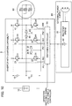
- Fig. 1 illustrates a configuration example of an inverter 1 with charging capability of a first embodiment.
- the inverter 1 with charging capability controls, with the motor current supplied, for example, to a three-phase permanent-magnet type synchronous motor (hereinafter, motor) 60, a driving torque generated by the motor 60 and also controls to charge the power of an external power supply 80 to a battery 70.
- motor three-phase permanent-magnet type synchronous motor
- the inverter 1 with charging capability includes a first capacitor 10, a second capacitor 11, a first diode 12, a second diode 13, upper arm switching elements 21, 31, and 41, and lower arm switching elements 22, 32, and 42.
- This example includes a plurality of arm circuits (U-phase, V-phase, and W-phase) in which an upper arm and a lower arm are connected.
- the positive electrode of the battery 70 is connected to the upper arm switching elements 21, 31, and 41, respectively.
- the negative electrode of the battery 70 is connected to the lower arm switching elements 22, 32, and 42, respectively.
- the upper arm switching element 21 and the lower arm switching element 22 are connected to each other to constitute the U-phase arm circuit.
- the upper arm switching element 31 and the lower arm switching element 32 are connected to each other to constitute the V-phase arm circuit.
- the upper arm switching element 41 and the lower arm switching element 42 are connected to each other to constitute the W-phase arm circuit.
- One end of the first capacitor 10 is connected to the positive electrode of the battery 70.
- the second capacitor 11 connects between the other end of the first capacitor 10 and the negative electrode of the battery 70.
- the cathode electrode of the first diode 12 is connected to the connection point between the U-phase upper arm switching element 21 and the U-phase lower arm switching element 22.
- the cathode electrode of the second diode 13 is connected to the other end of the first capacitor 10.
- a rectifier bridge 81 of the external power supply 80 is connected to a feeding point A at which the anode electrode of the first diode 12 and the anode electrode of the second diode 13 are connected to each other.
- the rectifier bridge 81 is an ordinary one which rectifies the alternating current (AC) of the external power supply 80.
- the external power supply 80 may be a three-phase AC power supply or may be a single-phase AC power supply
- Each of the upper arm switching elements 21, 31, and 41 and the lower arm switching elements 22, 32, and 42 includes an NMOSFET, for example.
- the respective switching elements 21, 31, 41, 22, 32, and 42 may include an IGBT (Insulated Gate Bipolar Transistor), a GTO (Gate Turn Off thyristor), or the like.
- the respective switching elements 21, 22, 31, 32, 41, and 42 have respective diodes D1, D2, D3, D4, D5, and D6 connected in antiparallel thereto.
- a signal PU output by a switching controller 50 is input to the gate electrode of the U-phase upper arm switching element 21.
- a signal NU output by the switching controller 50 is input to the gate electrode of the same U-phase lower arm switching element 22.
- a signal PV output by the switching controller 50 is input to the gate electrode of the V-phase upper arm switching element 31.
- a signal NV output by the switching controller 50 is input to the gate electrode of the same V-phase lower arm switching element 32.
- a signal PW output by the switching controller 50 is input to the gate electrode of the W-phase upper arm switching element 41.
- a signal NW output by the switching controller 50 is input to the gate electrode of the same W-phase lower arm switching element 42.
- connection point between the switching element 21 and switching element 22 constituting the U-phase arm circuit is connected to a U-phase motor coil 60u of the motor 60.
- connection point between the switching element 31 and switching element 32 constituting the V-phase arm circuit is connected to a V-phase motor coil 60v of the motor 60.
- connection point between the switching element 41 and switching element 42 constituting the W-phase arm circuit is connected to a W-phase motor coil 60w of the motor 60.
- the switching controller 50 switches a control logic based on an operation switching signal from a non-illustrated vehicle controller which controls, for example, the operation of the electric vehicle.
- the control logic of the switching controller 50 includes two control logics: a load control logic for driving the motor 60 with a direct current (DC) power stored in the battery 70; and a charge control logic for charging the power supplied from the external power supply 80 to the battery 70.
- DC direct current
- Fig. 2 illustrates a logic configuration when the switching controller 50 is realized with a microcomputer, for example.
- the switching controller 50 constituted from an arithmetic processing unit of the microcomputer includes a load control logic unit 51, a charge control logic unit 52, and a logic switching unit 53.
- the load control logic unit 51 monitors the load current flowing in each phase of the motor 60, and generates a PWM (Pulse Width Modulation) signal for controlling the drive voltage of each phase so that a load current corresponding to a current command from a non-illustrated vehicle controller flows.
- the PWM signal refers to each of the above-described signals PU, NU, signals PV, NV, and signals PW, NW.
- the charge control logic unit 52 generates a PWM signal for charging the power from the external power supply to the battery 70 in accordance with the output voltage of the rectifier bridge 81 which rectifies the alternating current of the external power supply 80.
- the charging is performed by boosting the output voltage of the rectifier bridge 81 using each of the motor coils 60u, 60v, and 60w of the motor 60.
- the logic switching unit 53 selects, when the operation switching signal is in a state of driving the motor 60, a PWM signal generated by the load control logic unit 51. Note that the PWM signal generated by the load control logic unit 51 is the same as the PWM signal when the conventional inverter drives a motor.
- the PWM signal output by the charge control logic unit 52 will be explained with reference to Fig. 3 .
- the signal NW which is the PWM signal output by the charge control logic unit 52 (switching controller 50)
- the signal PU which is also a PWM signal
- U-phase voltage to which the cathode electrode of the first diode 12 is connected the operation state of the first diode 12, and the charge mode of the charge control logic.
- the horizontal direction of Fig. 3 represents time.
- An interval during which the amplitude in the vertical direction is high (High: “1") represents the interval for turning on each switching element, while an interval during which the amplitude in the vertical direction is low (Low: "0") represents the interval for turning off each switching element.
- Vdc/n and Vdc in the view represent voltage values.
- Vdc is the voltage of the positive electrode of the battery 70.
- Vdc/n is the voltage obtained by dividing Vdc with the first capacitor 10 and second capacitor 11 in this example. If the capacitances of the first capacitor 10 and the second capacitor 11 are the same, the voltage is Vdc/2.
- the output of the rectifier bridge 81 is connected to the anode electrodes of the first diode 12 and second diode 13, i.e., the feeding point A, via a rectifier diode 82.
- the output voltage of the rectifier bridge 81 is higher than Vdc/2 in the interval t 1
- a current flows through the rectifier diode 82, the first diode 12, the motor coil 60u, the motor coil 60w, and the switching element 42.
- the operation state of the first diode 12 in this case is a conduction state in which a current flows to the motor 60 from the external power supply 80. Therefore, the charge mode of the charge control logic in the interval t 1 is referred to as a "conduction mode.”
- the magnetic energy by the current in this "conduction mode" is stored in the motor coils 60u and 60w.
- the rectifier diode 82 acts as a backflow prevention diode.
- the output of the rectifier bridge 81 and the second capacitor 11 are isolated from each other and the voltage of the anode electrode of the second diode 13 is maintained at Vdc/2 clamped by the second diode 13.
- the voltage of the anode electrode of the second diode 13 can be stabilized at Vdc/2 even if the output voltage of the rectifier bridge 81 varies.
- the voltage of the anode electrode of the second diode 13 is actually Vdc/2+VF (the forward voltage of the second diode 13). Accordingly, the U-phase voltage becomes Vdc/2 which is the resultant voltage reduced by the forward voltage VF of the first diode 12.
- the inverter 1 with charging capability of the present embodiment can stabilize the potential at the feeding point A to which the power of the external power supply 80 is supplied, without using a large reactance.
- the magnetic energy stored in the motor coils 60u and 60w in the interval t 1 can be recovered as a self-induction electromotive force generated by self-inductance effect.
- the magnetic energy stored in the motor coils 60u and 60w generates a boosted voltage waveform (self-induction electromotive force) corresponding to this energy in the U-phase voltage at the moment when the interval t 2 starts.
- the boosted voltage waveform (self-induction electromotive force) generated in the U-phase charges the battery 70 via the diode D1.
- the first diode 12 acts as a backflow prevention diode with respect to this boosted voltage waveform. Accordingly, the charging current flowing by this boosted voltage waveform will flow only into the battery 70 via the diode D 1.
- the operation state of the first diode 12 in the interval t 2 is a blocking state because the first diode 12 acts as a backflow prevention diode with respect to this boosted voltage waveform.
- the charge mode of the charge control logic in the interval t 2 is referred to as a "boost mode" because a boosted voltage waveform is generated.
- the time width of the interval t 2 may be shorter than the time width of the interval t 1 .
- the U-phase upper arm switching element 21 is turned on. If the U-phase upper arm switching element 21 is turned on, the boosted voltage waveform charges the battery 70 via the switching element 21. Moreover, once the switching element 21 is turned on, the U-phase voltage becomes Vdc which is the voltage of the positive electrode of the battery 70.
- the U-phase upper arm switching element 21 resets the U-phase voltage to Vdc. That is, in the interval t 3 , turning on the switching element 21 prevents the U-phase voltage from becoming unstable due to the boosted voltage waveform. Therefore, the signal PU in the interval t 3 may be referred to as a reset pulse.
- the boosted-voltage can be controlled by controlling a phase difference from turning on the W-phase lower arm switching element 42 and to turning on the U-phase upper arm switching element 21.
- the reason why the phase difference is set to the one from turning on the W-phase lower arm to turning on the U-phase upper arm is that the time width of the interval t 2 may be short as described above.
- the boosted voltage waveform self-induction electromotive force
- the operation state of the first diode 12 in the interval t 3 is the blocking state in which the first diode 12 acts as a backflow prevention diode because the switching element 21 is turned on to reset the U-phase voltage to Vdc.
- the charge mode of the charge control logic in the interval t 3 is referred to as a "recirculation mode", because the boosted voltage waveform (self-induction electromotive force) generated in the interval t 2 is recirculated to the battery 70.
- the charge control logic unit 52 generates a PWM signal for repeating the above-described intervals t 1 to t 3 .
- An interval t 4 is the same as the interval t 1 .
- An interval t 5 is the same as the interval t 2 .
- An interval t 6 is the same as the interval t 3 .
- the charge control logic unit 52 repeats the intervals t 1 to t 3 also in an interval t 7 and thereafter.
- the potential at the feeding point A can be stabilized without using a large reactance. Therefore, the inverter 1 with charging capability can be reduced in size.
- the W-phase lower arm switching element 42 and the U-phase upper arm switching element 21 are turned on/off at a predetermined cycle, but not limited to this example.
- the V-phase lower arm switching element 32 and the U-phase upper arm switching element 21 may be turned on/off.
- the cathode electrode of the first diode 12 may be connected to the connection point between the V-phase upper arm switching element 31 and the V-phase lower arm switching element 32.
- the V-phase upper arm switching element 31 and, for example, the U-phase lower arm switching element 22 are turned on/off.
- the cathode electrode of the first diode 12 may be connected to the connection point between the W-phase upper arm switching element 41 and the W-phase lower arm switching element 42.
- the W-phase upper arm switching element 41 and, for example, the V-phase lower arm switching element 32 are turned on/off.
- the upper arm and lower arm to be turned on/off only need to be different from each other in this manner.
- the inverter 1 with charging capability can charge the battery 70 by controlling a phase difference for turning on a lower arm switching element of a phase, to which the first diode 12 is not connected, and turning on an upper arm switching element of a phase, to which the first diode 12 is connected.
- the inverter 1 with charging capability can dispense with a large reactance to reduce the size of the inverter 1 with charging capability
- the inverter 1 with charging capability does not have an adversely effect on the reliability or life of the battery 70.
- Fig. 4 illustrates a configuration example of an inverter 2 with charging capability of a second embodiment.
- the inverter 2 with charging capability of the present embodiment differs from the inverter 1 with charging capability ( Fig. 1 ) in that it includes a first switching element 20 connected in parallel to the first diode 12.
- the horizontal axis of Fig. 5 represents voltage V, while the vertical axis represents current 1.
- a thick solid line indicates the V-I characteristic of the first diode 12.
- a narrow solid line indicates the V-I characteristic of the first switching element 20.
- the voltage needed to feed a current I 1 through the first diode 12 is V 2 .
- the voltage needed to feed the same current I 1 through the first switching element 20 is V 1 . Because the first diode 12 has the forward voltage VF on the order of 0.7 V, the relationship of V 2 >V 1 is always satisfied.
- the power (I 1 ⁇ (V 2 -V 1 )) by this voltage difference results in a loss.
- the first switching element 20 may be turned on in the interval t 1 (conduction mode) in which the first diode 12 does not act as the backflow prevention diode.
- the first switching element 20 is turned on when the charge mode of the charge control logic is the "conduction mode.” By turning on the first switching element 20, the voltage drop corresponding to the forward voltage VF of the first diode 12 can be eliminated from the path of the charging current.
- the inverter 2 with charging capability can improve the charging efficiency by the amount of the eliminated voltage drop.
- Fig. 6 illustrates the timings for turning on the W-phase lower arm switching element 42 and the first switching element 20.
- the horizontal direction of Fig. 6 represents time, while the vertical direction represents the amplitude of a signal.
- the W-phase lower arm switching element 42 and the first switching element 20 are turned on by an amplitude "1.”
- the signal input to the gate electrode of the first switching element 20 is set to the same as the signal NW.
- the amplitude of the signal NW becomes "0" (interval t 2 )
- a boosted voltage waveform self-induction electromotive force
- the amount of variation of the current may decrease due to a subtle delay of the signals. For example, if the first switching element 20 is turned off earlier, the current flowing through the W-phase lower arm switching element 42 will decrease by the amount of the forward voltage VF of the first diode 12. As the result, the amount of variation of the current at the moment of turning off the switching element 42 also decreases, so the self-induction electromotive force also decreases.
- the signal for stabilizing the generation of the self-induction electromotive force is illustrated as a stabilization signal, in Fig. 6 .
- the stabilization signal is obtained by making the ON time of the first switching element 20 longer by a time period ⁇ than the ON time of the W-phase lower arm switching element 42.
- the first switching element 20 can be used for various types of devices. For example, an IGBT or a MOSFET can be used. Moreover, a relay having a contact point may be used. If the first switching element 20 is constituted from an NMOSFET, the first diode 12 can be eliminated. This point will be explained in the next embodiment.
- Fig. 7 illustrates a configuration example of an inverter 3 with charging capability of a third embodiment.
- the inverter 3 with charging capability of the present embodiment differs from the inverter 2 with charging capability ( Fig. 4 ) in that the first diode 12 and first switching element 20 are configured as one device 30.
- the device 30 is an NMOSFET.
- the device 30 includes an NMOSFET 30a and a first parasitic diode 30b.
- the first parasitic diode 30b is a diode which is inevitably included due to the semiconductor structure of an NMOSFET.
- the first parasitic diode 30b acts similarly to the first diode 12.
- the anode electrode of the first parasitic diode 30b is a semiconductor substrate (p-type) which is biased to the same potential as the source electrode of the NMOSFET 30a. Moreover, the cathode electrode thereof is the drain electrode of the n-type semiconductor.
- the inverter 3 with charging capability exhibits the effects of achieving a reduction in size and a reduction in cost of the inverter 2 with charging capability because it can eliminate the first diode 12 ( Fig. 4 ) which is a discrete component. Note that the inverter 3 with charging capability exhibits the same operational effect as the inverter 2 with charging capability.
- the built-in voltage is a potential difference generated by the electric field inside a depletion layer region of a p-n junction, and is the voltage equivalent to the above-described forward voltage VF.
- Fig. 8 illustrates a configuration example of an inverter 4 with charging capability of a fourth embodiment.
- the inverter 4 with charging capability of the present embodiment differs from the inverter 1 with charging capability ( Fig. 1 ) in that it includes a plurality of feeding points to which power is supplied from the external power supply 80 and that it includes a switching controller 54.
- the inverter 4 with charging capability includes a third diode 33 and a fourth diode 34.
- the third diode 33 has the cathode electrode connected to a connection point of an arm circuit (phase) different from the connection point to which the first diode 12 is connected.
- the cathode electrode of the third diode 33 is connected to the connection point of the V-phase arm circuit.
- the fourth diode 34 is connected between the first capacitor 10 and the third diode 33.
- the anode electrode of the fourth diode 34 is connected to the anode electrode of the third diode 33, and constitutes a feeding point B to which power is supplied from the external power supply 80.
- the cathode electrode of the fourth diode 34 is connected to the voltage of Vdc/2 at the other end of the first capacitor 10.
- the output signal of the rectifier bridge 81 of the external power supply 80 is connected via the rectifier diode 82 to the feeding point B, as to the feeding point A. Accordingly, as with the feeding point A, the voltage of the feeding point B can be stabilized without using a large reactance.
- the signal PV for turning on/off the V-phase upper arm switching element 31 is the above-described reset pulse.
- the first diode 12 and third diode 33 of the inverter 4 with charging capability operate in the "conduction mode" in the interval t 1 , respectively. Because the first diode 12 and the third diode 33 operate in the "conduction mode", the current flowing from the external power supply 80 to the motor 60 increases.
- the magnetic energy by the current in this "conduction mode” is stored in the motor coils 60u and 60w and in the motor coils 60v and 60w.
- This stored magnetic energy will increase by the amount of an increase in the current than in the case of the inverter 1 with charging capability.
- This magnetic energy generates, in the U-phase voltage and V-phase voltage, a boosted voltage waveform (self-induction electromotive force) corresponding to each energy thereof at the moment when the interval t 2 starts.
- the subsequent operation is the same as that of the inverter 1 with charging capability.
- the inverter 4 with charging capability including a plurality of feeding points can increase the charging power more than the inverter 1 with charging capability having one feeding point.
- a configuration other than a combination of the feeding points A and B can be also contemplated. Then, a modified example of the inverter 4 with charging capability will be explained.
- Fig. 10 illustrates a configuration example of an inverter 5 with charging capability of a modification of the inverter 4 with charging capability
- the inverter 5 with charging capability of the present embodiment differs in that it includes a feeding point C in place of the feeding point A of the inverter 4 with charging capability.
- the inverter 5 with charging capability of the present embodiment differs from the inverter 4 with charging capability in that it includes a switching controller 55.
- the feeding point C is constituted by connecting the anode electrode of a fifth diode 43 having the cathode electrode connected to the connection point of the W-phase arm circuit and the anode electrode of a sixth diode 44 having the cathode electrode connected to the other end of the first capacitor 10.
- the current supplied to the feeding point C from the external power supply 80 flows through the fifth diode 43, the motor coil 60w, the motor coil 60u, and the U-phase lower arm switching element 22.
- the inverter 5 with charging capability differs from the inverter 4 with charging capability in that the lower arm switching element for feeding the current therethrough is the U-phase lower arm switching element 22.
- the W-phase lower arm switching element 42 is turned on/off.
- the signal input to the gate electrode of the U-phase lower arm switching element 22 is set to be the same as the U signal NW of Fig. 9 .
- the signal input to the gate electrode of each of the V-phase upper arm switching element 31 and W-phase upper arm switching element 41 is set to be the same as the signal PU of Fig. 9 .
- the method for controlling to turn on/off the U-phase lower arm switching element 22, the V-phase upper arm switching element 31, and the W-phase upper arm switching element 41, respectively, is the same as in the inverter 4 with charging capability.
- the switching controllers 54 and 55 of the inverters 4 and 5 with charging capability each including a plurality of feeding points charge the battery 70 by controlling a phase difference of the on-timing between a lower arm switching element of the arm circuit not to be supplied with power and an upper arm switching element of the arm circuit to be supplied with power. Note that, even a configuration of combining the feeding point A for supplying power to the U-phase arm circuit and the feeding point C for supplying power to the W-phase arm circuit exhibits the similar operational effect. Note that the illustration of a functional configuration example of an inverter with charging capability in which the feeding point A and feeding point C are combined is omitted.
- Fig. 11 illustrates a configuration example of an inverter 6 with charging capability of a fifth embodiment.
- the inverter 6 with charging capability of the present embodiment differs from the inverter 1 with charging capability ( Fig. 1 ) in that it includes the feeding points A, B, and C via which power is supplied to the U-phase, V-phase, and W-phase from the external power supply 80, respectively, and that it includes a switching controller 56.
- the switching controller 56 turns on/off the U-phase lower arm switching element 22 to which the first diode 12 is connected, the V-phase lower arm switching element 32 to which the third diode 33 is connected, and the W-phase lower arm switching element 42 to which the fifth diode 43 is connected.
- the switching controller 56 turns on/off the switching elements 22, 32, and 42 with an ON time of a time width during which the currents flowing through the respective switching elements 22, 32, and 42 are not shorted.
- the time width during which the currents are not shorted is a time width during which a short-circuit current will not flow, even if the switching elements 22, 32, and 42 are turned on, due to the inductance component of a feeder for supplying power to each of the feeding points A, B, and C from the external power supply 80.
- This inductance component may be a parasitic inductance or may be a finite inductance component.
- an inductance of a discrete component is inserted and added between each of the feeding points A, B, C and the rectifier diode 82.
- Fig. 12 illustrates the signal NU, signal NV, and signal NW that are the examples of the waveform of the signal which the switching controller 56 outputs to the respective switching elements 22, 32, and 42.
- Fig. 12(a) illustrates the waveforms in a long horizontal axis (in a long period time).
- Fig. 12(b) illustrates the waveforms in a short horizontal axis (in a short period time).
- Fig. 12(a) From the top of Fig. 12(a) , there are illustrated the signal NU input to the gate electrode of the U-phase lower arm switching element 22, the signal NV input to the gate electrode of the V-phase lower arm switching element 32, and the signal NW input to the gate electrode of the W-phase lower arm switching element 42.
- the switching controller 56 turns on/off the lower arm switching element of each phase after providing a dead time of a short time width during which the current flowing through each switching element does not result in a short-circuit current.
- the phases of the respective phases are described as being aligned, but not necessarily limited thereto, and a phase difference may be provided.
- a boosted voltage waveform (self-induction electromotive force) is generated in each phase voltage.
- This boosted voltage waveform generated in each phase charges the battery 70 via the diode D1, D2 or D3.
- Fig. 12(b) From the top of Fig. 12(b) , there are illustrated the signals NU, PU, the signals NV, PV, and the signals NW, PW.
- the signals PU, PV, and PW are the signals obtained by inverting the signals NU, NV, and NW, respectively.
- the lower arm switching elements 22, 32, and 42 of the respective phases are turned on/off with a short time width. Turning on/off the lower arm switching elements 22, 32, and 42 with a short time width allows the battery 70 to be charged even if power is supplied from the external power supply 80 to all of the three phases.
- Fig. 13 illustrates a configuration example of an inverter 7 with charging capability of a sixth embodiment.
- the inverter 7 with charging capability of the present embodiment differs from the inverter 6 with charging capability ( Fig. 11 ) in that it includes a switching controller 57 and that it includes an external power supply 90 which rectifies, for each phase, and outputs the alternating current of a three-phase AC power supply.
- the external power supply 90 includes a rectifier 91.
- the rectifier 91 outputs the output voltage obtained by rectifying each phase of the three-phase AC power supply.
- a diode 92 supplies the output voltage obtained by rectifying the alternating current of the U-phase to the feeding point A.
- a diode 93 supplies the output voltage obtained by rectifying the alternating current of the V-phase to the feeding point B.
- a diode 94 supplies the output voltage obtained by rectifying the alternating current of the W-phase to the feeding point C.
- the output voltage output by the rectifier 91 is output independently for each phase. That is, when the rectification waveform of the U-phase is being output, the output voltages of the V-phase and W-phase are zero. When the rectification waveform of the V-phase is being output, the output voltages of the U-phase and W-phase are zero. When the rectification waveform of the W-phase is being output, the output voltages of the U-phase and V-phase are zero.
- the switching controller 57 includes a U-phase controller 570 which turns on/off the switching element of an arm circuit in accordance with the output voltage of the U-phase, a V-phase controller 571 corresponding to the output voltage of the V-phase, and a W-phase controller 572 corresponding to the output voltage of the W-phase.
- the U-phase controller 570 controls, in the phase during which current can be supplied to the motor 60 from the first diode 12, a phase difference of the on-timing between the U-phase upper arm switching element 21 and, for example, the W-phase lower arm switching element 42.
- the U-phase upper arm and the V-phase lower arm may be turned on/off.
- the V-phase controller 571 controls, in the phase during which current can be supplied to the motor 60 from the third diode 33, a phase difference of the on-timing between the V-phase upper arm switching element 21 and, for example, the U-phase lower arm switching element 22. Moreover, the V-phase upper arm and the W-phase lower arm may be turned on/off.
- the W-phase controller 572 controls, in the phase during which current can be supplied to the motor 60 from the fifth diode 43, a phase difference of the on-timing between the W-phase upper arm switching element 41 and, for example, the V-phase lower arm switching element 32. Moreover, the W-phase upper arm and the U-phase lower arm may be turned on/off.
- the inverter 7 with charging capability can also control so that the rotor of the motor 60 will not rotate.
- the rotor may not be mechanically fixed during charging.
- Fig. 14 illustrates a configuration example of an inverter 8 with charging capability of a seventh embodiment.
- the inverter 8 with charging capability is an inverter capable of performing the PWM control of three levels.
- the inverter 8 with charging capability of the present embodiment differs from the inverter 6 with charging capability ( Fig. 11 ) in that it includes a switching element connected in parallel to a diode constituting each of the feeding points A, B, and C.
- the first switching element 20 is connected in parallel to the first diode 12.
- a second switching element 92 is connected in parallel to the second diode 13.
- a third switching element 93 is connected in parallel to the third diode 33.
- a fourth switching element 94 is connected in parallel to the fourth diode 34.
- a fifth switching element 95 is connected in parallel to the fifth diode 43.
- a sixth switching element 96 is connected in parallel to the sixth diode 44.
- the potential of Vdc/2 can be supplied to the V-phase by simultaneously conducting the third switching element 93 and fourth switching element 94. Moreover, in order to supply the potential of Vdc/2 to the W-phase, the fifth switching element 95 and the sixth switching element 96 may be simultaneously conducted.
- the inverter 8 with charging capability in addition to two voltages, i.e., the voltage (Vdc) of the positive electrode and the voltage of the negative electrode of the battery 70, Vdc/2 which is the third voltage can be supplied to the AC side of the inverter. Accordingly, the inverter 8 with charging capability enables the PWM control of three levels.
- the on/off control of the first switching element 20, second switching element 92, ..., and the sixth switching element 96 is performed by a load control logic unit (corresponding to the load control logic unit 51 illustrated in Fig. 2 ) inside a switching controller 58.
- a load control logic unit corresponding to the load control logic unit 51 illustrated in Fig. 2
- the conventional method for a three-level inverter can be used.
- the inverter 8 with charging capability generates an AC waveform using the DC voltages of three levels, a smoother AC waveform can be generated. As the result, the vibration of the motor 60 is reduced and noise is also reduced. Moreover, the inverter 8 with charging capability exhibits also the operational effect of dispensing with a large reactance intended to stabilize the potential of a feeding point, as with the inverter 6 with charging capability ( Fig. 11 ).
- the potential at the feeding point A can be stabilized without using the conventionally-used large reactance. Accordingly, the inverter with charging capability can be reduced in size.
- the inverter 2 with charging capability ( Fig. 4 ) of the second embodiment by turning on the first switching element 20 when the charge mode is the "conduction mode", it is possible to eliminate the voltage drop corresponding to the forward voltage VF of the first diode 12 from the path of the charging current to improve the charging efficiency.
- the first diode 12 and the first switching element 20 can be configured as one device 30 (NMOSFET). Accordingly, the inverter 3 with charging capability exhibits an effect of achieving a further reduction in size as compared with the inverter 2 with charging capability.
- the charging power charged from the external power supply 80 to the battery 70 can be increased more than any of the inverters 1 to 3 with charging capability each having one feeding point because the inverters 4 and 5 with charging capability each include a plurality of feeding points.
- the inverter 4 with charging capability may be combined with the second embodiment or third embodiment.
- the inverter 6 with charging capability ( Fig. 11 ) of the fifth embodiment power is supplied from the external power supply 80 to all of the plurality of phases and the lower arm switching elements 22, 32, and 42 of the respective phases are turned on/off with a short time width.
- the currents flowing through the switching elements 22, 32, and 42 do not result in a short-circuit current even if power is supplied from the external power supply 80 to all of the three phases, and the battery 70 can be charged.
- the switching controller 57 includes the U-phase controller 570, V-phase controller 571, and W-phase controller 572 which turn on/off the switching element of an arm circuit in accordance with the output voltage of each phase of the AC power supply. Because the U-phase controller 570, the V-phase controller 571, and the W-phase controller 572 each independently turn on/off a switching element, the power-supply high frequency component generated during charging can be reduced and the normal mode noise given to the battery 70 can be reduced.
- PWM control of three levels is enabled in addition to the operational effect of dispensing with a large reactance exhibited by the above-described embodiments.
- the PWM control of three levels can reduce the vibration of the motor 60 and also reduce noise.
- Vdc/2 has been illustrated as a specific example of Vdc/n, n may be an integer equal to or greater than 2.
- the diodes D1 to D6 connected in antiparallel to the NMOSFETs of the upper arm switching elements 21, 31, and 41 and lower arm switching elements 22, 32, and 42 may be the above-described parasitic diodes.
Landscapes
- Engineering & Computer Science (AREA)
- Power Engineering (AREA)
- Life Sciences & Earth Sciences (AREA)
- Sustainable Development (AREA)
- Sustainable Energy (AREA)
- Transportation (AREA)
- Mechanical Engineering (AREA)
- Inverter Devices (AREA)
- Charge And Discharge Circuits For Batteries Or The Like (AREA)
- Dc-Dc Converters (AREA)
Abstract
Description
- The present invention relates to an inverter with charging capability which can be also used as a charging unit.
- An electric vehicle, such as the conventional electric car or hybrid car, is provided with an inverter, which controls driving of a motor. The examples of this inverter include the one that performs (is used in common for) the drive control of a motor and the charge control of a battery.
- This inverter with charging capability boosts, in receipt of power from an external power supply, the voltage of the external power supply by a switching operation of the inverter and charges power to the battery of an electric vehicle. Conventionally, the inverter with charging capability and the external power supply are connected to each other via a reactance including a coil (Patent Literature 1).
- Patent Literature 1: Japanese Laid-open Patent Publication No.
2002-223559 - In order to electrically stabilize a feeding point of an inverter with charging capability, it is necessary to connect the inverter with charging capability with an external power supply via a reactance. The reactance causes an increase in size of the conventional inverter with charging capability.
- The present invention has been made in view of this problem, and provides an inverter with charging capability which can dispense with a large reactance to achieve reduction in size.
- An inverter with charging capability according to an aspect of the present invention includes an arm circuit, a first capacitor, a second capacitor, a first diode, and a second diode. The arm circuit includes upper arm and lower arm switching elements connected to a battery One end of the first capacitor is connected to the positive electrode of the battery. The second capacitor is connected between the other end of the first capacitor and the negative electrode of the battery. The first diode has a cathode electrode connected to a connection point between the upper arm and lower arm switching elements. The cathode electrode of the second diode is connected to the other end of the first capacitor. Then, in the inverter with charging capability according to an aspect of the present invention, power is supplied from an external power supply to the anode electrode of the first diode and the anode electrode of the second diode.
-
- [
Fig. 1] Fig. 1 illustrates a configuration example of aninverter 1 with charging capability of a first embodiment. - [
Fig. 2] Fig. 2 illustrates a functional configuration example of aswitching controller 50 of theinverter 1 with charging capability. - [
Fig. 3] Fig. 3 illustrates an example of the time chart of the switching control performed by theswitching controller 50. - [
Fig. 4] Fig. 4 illustrates a configuration example of aninverter 2 with charging capability of a second embodiment. - [
Fig. 5] Fig. 5 illustrates the voltage-current characteristics of afirst diode 12 and afirst switching element 20. - [
Fig. 6] Fig. 6 illustrates the timings for turning on thefirst diode 12 and thefirst switching element 20. - [
Fig. 7] Fig. 7 illustrates a configuration example of aninverter 3 with charging capability of a third embodiment. - [
Fig. 8] Fig. 8 illustrates a configuration example of aninverter 4 with charging capability of a fourth embodiment. - [
Fig. 9] Fig. 9 illustrates an example of the time chart of the switching control performed by aswitching controller 54 of theinverter 4 with charging capability. - [
Fig. 10] Fig. 10 illustrates a configuration example of aninverter 5 with charging capability of a modification of theinverter 4 with charging capability. - [
Fig. 11] Fig. 11 illustrates a configuration example of aninverter 6 with charging capability of a fifth embodiment. - [
Fig. 12] Fig. 12(a) illustrates an example of the time chart for a long period time of the switching control performed by aswitching controller 56 of theinverter 6 with charging capability, whileFig. 12(b) illustrates an example for a short period time. - [
Fig. 13] Fig. 13 illustrates a configuration example of aninverter 7 with charging capability of a sixth embodiment. - [
Fig. 14] Fig. 14 illustrates a configuration example of aninverter 8 with charging capability of a seventh embodiment. - Embodiments will be described with reference to the drawings. In the description of the drawings, the same part is given the same reference sign to omit the description thereof.
-
Fig. 1 illustrates a configuration example of aninverter 1 with charging capability of a first embodiment. Theinverter 1 with charging capability controls, with the motor current supplied, for example, to a three-phase permanent-magnet type synchronous motor (hereinafter, motor) 60, a driving torque generated by themotor 60 and also controls to charge the power of anexternal power supply 80 to abattery 70. - The
inverter 1 with charging capability includes afirst capacitor 10, asecond capacitor 11, afirst diode 12, asecond diode 13, upperarm switching elements arm switching elements - The positive electrode of the
battery 70 is connected to the upperarm switching elements battery 70 is connected to the lowerarm switching elements - The upper
arm switching element 21 and the lowerarm switching element 22 are connected to each other to constitute the U-phase arm circuit. The upperarm switching element 31 and the lowerarm switching element 32 are connected to each other to constitute the V-phase arm circuit. The upperarm switching element 41 and the lowerarm switching element 42 are connected to each other to constitute the W-phase arm circuit. - One end of the
first capacitor 10 is connected to the positive electrode of thebattery 70. Thesecond capacitor 11 connects between the other end of thefirst capacitor 10 and the negative electrode of thebattery 70. - The cathode electrode of the
first diode 12 is connected to the connection point between the U-phase upperarm switching element 21 and the U-phase lowerarm switching element 22. The cathode electrode of thesecond diode 13 is connected to the other end of thefirst capacitor 10. Arectifier bridge 81 of theexternal power supply 80 is connected to a feeding point A at which the anode electrode of thefirst diode 12 and the anode electrode of thesecond diode 13 are connected to each other. - The
rectifier bridge 81 is an ordinary one which rectifies the alternating current (AC) of theexternal power supply 80. Theexternal power supply 80 may be a three-phase AC power supply or may be a single-phase AC power supply - Each of the upper
arm switching elements arm switching elements respective switching elements respective switching elements - A signal PU output by a
switching controller 50 is input to the gate electrode of the U-phase upperarm switching element 21. A signal NU output by theswitching controller 50 is input to the gate electrode of the same U-phase lowerarm switching element 22. - A signal PV output by the
switching controller 50 is input to the gate electrode of the V-phase upperarm switching element 31. A signal NV output by theswitching controller 50 is input to the gate electrode of the same V-phase lowerarm switching element 32. - A signal PW output by the
switching controller 50 is input to the gate electrode of the W-phase upperarm switching element 41. A signal NW output by theswitching controller 50 is input to the gate electrode of the same W-phase lowerarm switching element 42. - The connection point between the
switching element 21 and switchingelement 22 constituting the U-phase arm circuit is connected to aU-phase motor coil 60u of themotor 60. The connection point between theswitching element 31 and switchingelement 32 constituting the V-phase arm circuit is connected to a V-phase motor coil 60v of themotor 60. The connection point between the switchingelement 41 and switchingelement 42 constituting the W-phase arm circuit is connected to a W-phase motor coil 60w of themotor 60. - The switching
controller 50 switches a control logic based on an operation switching signal from a non-illustrated vehicle controller which controls, for example, the operation of the electric vehicle. The control logic of the switchingcontroller 50 includes two control logics: a load control logic for driving themotor 60 with a direct current (DC) power stored in thebattery 70; and a charge control logic for charging the power supplied from theexternal power supply 80 to thebattery 70. - The operation of the switching
controller 50 will be explained with reference toFig. 2. Fig. 2 illustrates a logic configuration when the switchingcontroller 50 is realized with a microcomputer, for example. The switchingcontroller 50 constituted from an arithmetic processing unit of the microcomputer includes a loadcontrol logic unit 51, a chargecontrol logic unit 52, and alogic switching unit 53. - The load
control logic unit 51 monitors the load current flowing in each phase of themotor 60, and generates a PWM (Pulse Width Modulation) signal for controlling the drive voltage of each phase so that a load current corresponding to a current command from a non-illustrated vehicle controller flows. The PWM signal refers to each of the above-described signals PU, NU, signals PV, NV, and signals PW, NW. - Moreover, the charge
control logic unit 52 generates a PWM signal for charging the power from the external power supply to thebattery 70 in accordance with the output voltage of therectifier bridge 81 which rectifies the alternating current of theexternal power supply 80. The charging is performed by boosting the output voltage of therectifier bridge 81 using each of themotor coils motor 60. - The
logic switching unit 53 selects, when the operation switching signal is in a state of driving themotor 60, a PWM signal generated by the loadcontrol logic unit 51. Note that the PWM signal generated by the loadcontrol logic unit 51 is the same as the PWM signal when the conventional inverter drives a motor. - The PWM signal output by the charge
control logic unit 52 will be explained with reference toFig. 3 . From the top ofFig. 3 , there are illustrated the signal NW which is the PWM signal output by the charge control logic unit 52 (switching controller 50), the signal PU which is also a PWM signal, a U-phase voltage to which the cathode electrode of thefirst diode 12 is connected, the operation state of thefirst diode 12, and the charge mode of the charge control logic. The horizontal direction ofFig. 3 represents time. An interval during which the amplitude in the vertical direction is high (High: "1") represents the interval for turning on each switching element, while an interval during which the amplitude in the vertical direction is low (Low: "0") represents the interval for turning off each switching element. Note that Vdc/n and Vdc in the view represent voltage values. Vdc is the voltage of the positive electrode of thebattery 70. - In an interval t1 during which the signal NW is "1", only the W-phase lower arm switching element 42 (
Fig. 1 ) is ON and all the other switching elements are OFF. The U-phase voltage in this interval t1 is Vdc/n. Vdc/n is the voltage obtained by dividing Vdc with thefirst capacitor 10 andsecond capacitor 11 in this example. If the capacitances of thefirst capacitor 10 and thesecond capacitor 11 are the same, the voltage is Vdc/2. - The reason why the U-phase voltage becomes Vdc/2 in the interval t1 will be explained. The output of the
rectifier bridge 81 is connected to the anode electrodes of thefirst diode 12 andsecond diode 13, i.e., the feeding point A, via arectifier diode 82. - In this configuration, when the output voltage of the
rectifier bridge 81 is higher than Vdc/2, a current flows through therectifier diode 82, thesecond diode 13, and thesecond capacitor 11. As the result, the voltage of the anode electrode of thesecond diode 13 is clamped to Vdc/2 by the voltage clamp action of thesecond diode 13. - Moreover, in this case (the case where the output voltage of the
rectifier bridge 81 is higher than Vdc/2 in the interval t1), a current flows through therectifier diode 82, thefirst diode 12, themotor coil 60u, themotor coil 60w, and the switchingelement 42. The operation state of thefirst diode 12 in this case is a conduction state in which a current flows to themotor 60 from theexternal power supply 80. Therefore, the charge mode of the charge control logic in the interval t1 is referred to as a "conduction mode." The magnetic energy by the current in this "conduction mode" is stored in the motor coils 60u and 60w. - Moreover, when the output voltage of the
rectifier bridge 81 is lower than Vdc/2, therectifier diode 82 and thesecond diode 13 are reversely biased. Therefore, therectifier diode 82 acts as a backflow prevention diode. As the result, the output of therectifier bridge 81 and thesecond capacitor 11 are isolated from each other and the voltage of the anode electrode of thesecond diode 13 is maintained at Vdc/2 clamped by thesecond diode 13. - That is, according to the
inverter 1 with charging capability of the present embodiment, the voltage of the anode electrode of thesecond diode 13 can be stabilized at Vdc/2 even if the output voltage of therectifier bridge 81 varies. The voltage of the anode electrode of thesecond diode 13 is actually Vdc/2+VF (the forward voltage of the second diode 13). Accordingly, the U-phase voltage becomes Vdc/2 which is the resultant voltage reduced by the forward voltage VF of thefirst diode 12. - As described above, the
inverter 1 with charging capability of the present embodiment can stabilize the potential at the feeding point A to which the power of theexternal power supply 80 is supplied, without using a large reactance. - In an interval t2, if the signal NW varies from "1" to "0", the W-phase lower
arm switching element 42 is turned off. If the switchingelement 42 becomes OFF, the current having flown through therectifier diode 82, thefirst diode 12, themotor coil 60u, themotor coil 60w, and the switchingelement 42 in the interval t1 is shut off by the switchingelement 42. - Then, the magnetic energy stored in the motor coils 60u and 60w in the interval t1 can be recovered as a self-induction electromotive force generated by self-inductance effect. The magnetic energy stored in the motor coils 60u and 60w generates a boosted voltage waveform (self-induction electromotive force) corresponding to this energy in the U-phase voltage at the moment when the interval t2 starts.
- The boosted voltage waveform (self-induction electromotive force) generated in the U-phase charges the
battery 70 via the diode D1. Thefirst diode 12 acts as a backflow prevention diode with respect to this boosted voltage waveform. Accordingly, the charging current flowing by this boosted voltage waveform will flow only into thebattery 70 via thediode D 1. - The operation state of the
first diode 12 in the interval t2 is a blocking state because thefirst diode 12 acts as a backflow prevention diode with respect to this boosted voltage waveform. Note that the charge mode of the charge control logic in the interval t2 is referred to as a "boost mode" because a boosted voltage waveform is generated. Note that the time width of the interval t2 may be shorter than the time width of the interval t1. - Next, in an interval t3 during which the signal NW becomes "0" and the signal PU becomes "1", the U-phase upper
arm switching element 21 is turned on. If the U-phase upperarm switching element 21 is turned on, the boosted voltage waveform charges thebattery 70 via the switchingelement 21. Moreover, once the switchingelement 21 is turned on, the U-phase voltage becomes Vdc which is the voltage of the positive electrode of thebattery 70. - Turning on the U-phase upper
arm switching element 21 resets the U-phase voltage to Vdc. That is, in the interval t3, turning on the switchingelement 21 prevents the U-phase voltage from becoming unstable due to the boosted voltage waveform. Therefore, the signal PU in the interval t3 may be referred to as a reset pulse. - As described above, according to the
inverter 1 with charging capability, the boosted-voltage can be controlled by controlling a phase difference from turning on the W-phase lowerarm switching element 42 and to turning on the U-phase upperarm switching element 21. Here, the reason why the phase difference is set to the one from turning on the W-phase lower arm to turning on the U-phase upper arm is that the time width of the interval t2 may be short as described above. The boosted voltage waveform (self-induction electromotive force) can be increased by increasing this phase difference. - The operation state of the
first diode 12 in the interval t3 is the blocking state in which thefirst diode 12 acts as a backflow prevention diode because the switchingelement 21 is turned on to reset the U-phase voltage to Vdc. Note that the charge mode of the charge control logic in the interval t3 is referred to as a "recirculation mode", because the boosted voltage waveform (self-induction electromotive force) generated in the interval t2 is recirculated to thebattery 70. - The charge
control logic unit 52 generates a PWM signal for repeating the above-described intervals t1 to t3. An interval t4 is the same as the interval t1. An interval t5 is the same as the interval t2. An interval t6 is the same as the interval t3. The chargecontrol logic unit 52 repeats the intervals t1 to t3 also in an interval t7 and thereafter. - As described above, according to the
inverter 1 with charging capability of the present embodiment, the potential at the feeding point A can be stabilized without using a large reactance. Therefore, theinverter 1 with charging capability can be reduced in size. - Note that, in
Fig. 1 the W-phase lowerarm switching element 42 and the U-phase upperarm switching element 21 are turned on/off at a predetermined cycle, but not limited to this example. The V-phase lowerarm switching element 32 and the U-phase upperarm switching element 21 may be turned on/off. - Moreover, the cathode electrode of the
first diode 12 may be connected to the connection point between the V-phase upperarm switching element 31 and the V-phase lowerarm switching element 32. In this case, the V-phase upperarm switching element 31 and, for example, the U-phase lowerarm switching element 22 are turned on/off. - Moreover, the cathode electrode of the
first diode 12 may be connected to the connection point between the W-phase upperarm switching element 41 and the W-phase lowerarm switching element 42. In this case, the W-phase upperarm switching element 41 and, for example, the V-phase lowerarm switching element 32 are turned on/off. The upper arm and lower arm to be turned on/off only need to be different from each other in this manner. - In short, the
inverter 1 with charging capability can charge thebattery 70 by controlling a phase difference for turning on a lower arm switching element of a phase, to which thefirst diode 12 is not connected, and turning on an upper arm switching element of a phase, to which thefirst diode 12 is connected. Moreover, because the potential at the feeding point A becomes stable even without using a large reactance, theinverter 1 with charging capability can dispense with a large reactance to reduce the size of theinverter 1 with charging capability Moreover, because the potential at the feeding point A becomes stable, theinverter 1 with charging capability does not have an adversely effect on the reliability or life of thebattery 70. -
Fig. 4 illustrates a configuration example of aninverter 2 with charging capability of a second embodiment. Theinverter 2 with charging capability of the present embodiment differs from theinverter 1 with charging capability (Fig. 1 ) in that it includes afirst switching element 20 connected in parallel to thefirst diode 12. - The operational effect of the
first switching element 20 will be explained with reference toFig. 5 . The horizontal axis ofFig. 5 represents voltage V, while the vertical axis represents current 1. A thick solid line indicates the V-I characteristic of thefirst diode 12. A narrow solid line indicates the V-I characteristic of thefirst switching element 20. - The voltage needed to feed a current I1 through the
first diode 12 is V2. The voltage needed to feed the same current I1 through thefirst switching element 20 is V1. Because thefirst diode 12 has the forward voltage VF on the order of 0.7 V, the relationship of V2>V1 is always satisfied. - The power (I1×(V2-V1)) by this voltage difference results in a loss. In order to eliminate this loss, the
first switching element 20 may be turned on in the interval t1 (conduction mode) in which thefirst diode 12 does not act as the backflow prevention diode. - The
first switching element 20 is turned on when the charge mode of the charge control logic is the "conduction mode." By turning on thefirst switching element 20, the voltage drop corresponding to the forward voltage VF of thefirst diode 12 can be eliminated from the path of the charging current. Theinverter 2 with charging capability can improve the charging efficiency by the amount of the eliminated voltage drop. -
Fig. 6 illustrates the timings for turning on the W-phase lowerarm switching element 42 and thefirst switching element 20. The horizontal direction ofFig. 6 represents time, while the vertical direction represents the amplitude of a signal. The W-phase lowerarm switching element 42 and thefirst switching element 20 are turned on by an amplitude "1." - In order to simultaneously turn on the W-phase lower
arm switching element 42 and first switchingelement 20, the signal input to the gate electrode of thefirst switching element 20 is set to the same as the signal NW. When the amplitude of the signal NW becomes "0" (interval t2), a boosted voltage waveform (self-induction electromotive force) is generated in the U-phase voltage to charge thebattery 70. - Note that, by making the ON time of the
first switching element 20 longer than the ON time of the W-phase lowerarm switching element 42, it is possible to stabilize the generation of the self-induction electromotive force. The larger the amount of variation of the current at the moment of turning off the switchingelement 42, the larger the self-induction electromotive force becomes. - If the signal NW and the signal for controlling the on/off of the
first switching element 20 are set to be the same signal, the amount of variation of the current may decrease due to a subtle delay of the signals. For example, if thefirst switching element 20 is turned off earlier, the current flowing through the W-phase lowerarm switching element 42 will decrease by the amount of the forward voltage VF of thefirst diode 12. As the result, the amount of variation of the current at the moment of turning off the switchingelement 42 also decreases, so the self-induction electromotive force also decreases. - In order to prevent a reduction of the self-induction electromotive force, the
first switching element 20 only needs to be surely on when the switchingelement 42 is turned off. The signal for stabilizing the generation of the self-induction electromotive force is illustrated as a stabilization signal, inFig. 6 . The stabilization signal is obtained by making the ON time of thefirst switching element 20 longer by a time period α than the ON time of the W-phase lowerarm switching element 42. - By delaying the timing for turning off the
first switching element 20 from the timing for turning off the lowerarm switching element 42 in this manner, it is possible to obtain a stable boosted voltage waveform (self-induction electromotive force). Note that, when the U-phase lowerarm switching element 22 is turned on/off and also when the V-phase lowerarm switching element 32 is turned on/off, the same effect can be obtained if the ON time of thefirst switching element 20 is set to be longer than the ON times of these switching elements. - Note that various types of devices can be used for the
first switching element 20. For example, an IGBT or a MOSFET can be used. Moreover, a relay having a contact point may be used. If thefirst switching element 20 is constituted from an NMOSFET, thefirst diode 12 can be eliminated. This point will be explained in the next embodiment. -
Fig. 7 illustrates a configuration example of aninverter 3 with charging capability of a third embodiment. Theinverter 3 with charging capability of the present embodiment differs from theinverter 2 with charging capability (Fig. 4 ) in that thefirst diode 12 and first switchingelement 20 are configured as onedevice 30. - The
device 30 is an NMOSFET. Thedevice 30 includes anNMOSFET 30a and a firstparasitic diode 30b. The firstparasitic diode 30b is a diode which is inevitably included due to the semiconductor structure of an NMOSFET. The firstparasitic diode 30b acts similarly to thefirst diode 12. - The anode electrode of the first
parasitic diode 30b is a semiconductor substrate (p-type) which is biased to the same potential as the source electrode of theNMOSFET 30a. Moreover, the cathode electrode thereof is the drain electrode of the n-type semiconductor. - The
inverter 3 with charging capability exhibits the effects of achieving a reduction in size and a reduction in cost of theinverter 2 with charging capability because it can eliminate the first diode 12 (Fig. 4 ) which is a discrete component. Note that theinverter 3 with charging capability exhibits the same operational effect as theinverter 2 with charging capability. - That is, turning on the
NMOSFET 30a as with thefirst switching element 20 explained in theinverter 2 with charging capability allows the built-in voltage of the firstparasitic diode 30b to be eliminated from the path of the charging current. The built-in voltage is a potential difference generated by the electric field inside a depletion layer region of a p-n junction, and is the voltage equivalent to the above-described forward voltage VF. -
Fig. 8 illustrates a configuration example of aninverter 4 with charging capability of a fourth embodiment. Theinverter 4 with charging capability of the present embodiment differs from theinverter 1 with charging capability (Fig. 1 ) in that it includes a plurality of feeding points to which power is supplied from theexternal power supply 80 and that it includes a switchingcontroller 54. - The
inverter 4 with charging capability includes athird diode 33 and afourth diode 34. Thethird diode 33 has the cathode electrode connected to a connection point of an arm circuit (phase) different from the connection point to which thefirst diode 12 is connected. In this example, the cathode electrode of thethird diode 33 is connected to the connection point of the V-phase arm circuit. - The
fourth diode 34 is connected between thefirst capacitor 10 and thethird diode 33. The anode electrode of thefourth diode 34 is connected to the anode electrode of thethird diode 33, and constitutes a feeding point B to which power is supplied from theexternal power supply 80. The cathode electrode of thefourth diode 34 is connected to the voltage of Vdc/2 at the other end of thefirst capacitor 10. - The output signal of the
rectifier bridge 81 of theexternal power supply 80 is connected via therectifier diode 82 to the feeding point B, as to the feeding point A. Accordingly, as with the feeding point A, the voltage of the feeding point B can be stabilized without using a large reactance. - The charging operation when power is supplied from the
external power supply 80 to the feeding points A and B will be explained with reference toFig. 9 . The descriptions of the time chart from the signal NW to the charge mode illustrated inFig. 9 are the same as the explainedFig. 3 . In theinverter 4 with charging capability, thefirst diode 12 and thethird diode 33 operate in the same charge mode. - Turning on/off the W-phase lower
arm switching element 42 and the V-phase upperarm switching element 31 allows the power supplied to the feeding point B to charge thebattery 70. In this case, the signal PV for turning on/off the V-phase upperarm switching element 31 is the above-described reset pulse. - The path of the current from the feeding point B will be explained. When the output voltage of the
rectifier bridge 81 is higher than Vdc/2 in the interval t1, the current will flow through therectifier diode 82, thethird diode 33, themotor coil 60v, themotor coil 60w, and the switchingelement 42. - As described above, the
first diode 12 andthird diode 33 of theinverter 4 with charging capability operate in the "conduction mode" in the interval t1, respectively. Because thefirst diode 12 and thethird diode 33 operate in the "conduction mode", the current flowing from theexternal power supply 80 to themotor 60 increases. - The magnetic energy by the current in this "conduction mode" is stored in the motor coils 60u and 60w and in the motor coils 60v and 60w. This stored magnetic energy will increase by the amount of an increase in the current than in the case of the
inverter 1 with charging capability. This magnetic energy generates, in the U-phase voltage and V-phase voltage, a boosted voltage waveform (self-induction electromotive force) corresponding to each energy thereof at the moment when the interval t2 starts. The subsequent operation is the same as that of theinverter 1 with charging capability. - As described above, the
inverter 4 with charging capability including a plurality of feeding points can increase the charging power more than theinverter 1 with charging capability having one feeding point. Note that a configuration other than a combination of the feeding points A and B can be also contemplated. Then, a modified example of theinverter 4 with charging capability will be explained. -
Fig. 10 illustrates a configuration example of aninverter 5 with charging capability of a modification of theinverter 4 with charging capability Theinverter 5 with charging capability of the present embodiment differs in that it includes a feeding point C in place of the feeding point A of theinverter 4 with charging capability. Moreover, theinverter 5 with charging capability of the present embodiment differs from theinverter 4 with charging capability in that it includes a switchingcontroller 55. - The feeding point C is constituted by connecting the anode electrode of a
fifth diode 43 having the cathode electrode connected to the connection point of the W-phase arm circuit and the anode electrode of asixth diode 44 having the cathode electrode connected to the other end of thefirst capacitor 10. The current supplied to the feeding point C from theexternal power supply 80 flows through thefifth diode 43, themotor coil 60w, themotor coil 60u, and the U-phase lowerarm switching element 22. - The current supplied to the feeding point B from the
external power supply 80 flows through thethird diode 33, themotor coil 60v, themotor coil 60u, and the U-phase lowerarm switching element 22. As described above, theinverter 5 with charging capability differs from theinverter 4 with charging capability in that the lower arm switching element for feeding the current therethrough is the U-phase lowerarm switching element 22. In theinverter 4 with charging capability, the W-phase lowerarm switching element 42 is turned on/off. - In the
inverter 5 with charging capability, the signal input to the gate electrode of the U-phase lowerarm switching element 22 is set to be the same as the U signal NW ofFig. 9 . Moreover, the signal input to the gate electrode of each of the V-phase upperarm switching element 31 and W-phase upperarm switching element 41 is set to be the same as the signal PU ofFig. 9 . The method for controlling to turn on/off the U-phase lowerarm switching element 22, the V-phase upperarm switching element 31, and the W-phase upperarm switching element 41, respectively, is the same as in theinverter 4 with charging capability. - The switching
controllers inverters battery 70 by controlling a phase difference of the on-timing between a lower arm switching element of the arm circuit not to be supplied with power and an upper arm switching element of the arm circuit to be supplied with power. Note that, even a configuration of combining the feeding point A for supplying power to the U-phase arm circuit and the feeding point C for supplying power to the W-phase arm circuit exhibits the similar operational effect. Note that the illustration of a functional configuration example of an inverter with charging capability in which the feeding point A and feeding point C are combined is omitted. -
Fig. 11 illustrates a configuration example of aninverter 6 with charging capability of a fifth embodiment. Theinverter 6 with charging capability of the present embodiment differs from theinverter 1 with charging capability (Fig. 1 ) in that it includes the feeding points A, B, and C via which power is supplied to the U-phase, V-phase, and W-phase from theexternal power supply 80, respectively, and that it includes a switchingcontroller 56. - The switching
controller 56 turns on/off the U-phase lowerarm switching element 22 to which thefirst diode 12 is connected, the V-phase lowerarm switching element 32 to which thethird diode 33 is connected, and the W-phase lowerarm switching element 42 to which thefifth diode 43 is connected. The switchingcontroller 56 turns on/off the switchingelements respective switching elements - Here, the time width during which the currents are not shorted is a time width during which a short-circuit current will not flow, even if the switching
elements external power supply 80. This inductance component may be a parasitic inductance or may be a finite inductance component. For the finite inductance component, an inductance of a discrete component is inserted and added between each of the feeding points A, B, C and therectifier diode 82. -
Fig. 12 illustrates the signal NU, signal NV, and signal NW that are the examples of the waveform of the signal which the switchingcontroller 56 outputs to therespective switching elements Fig. 12(a) illustrates the waveforms in a long horizontal axis (in a long period time).Fig. 12(b) illustrates the waveforms in a short horizontal axis (in a short period time). - From the top of
Fig. 12(a) , there are illustrated the signal NU input to the gate electrode of the U-phase lowerarm switching element 22, the signal NV input to the gate electrode of the V-phase lowerarm switching element 32, and the signal NW input to the gate electrode of the W-phase lowerarm switching element 42. As described above, the switchingcontroller 56 turns on/off the lower arm switching element of each phase after providing a dead time of a short time width during which the current flowing through each switching element does not result in a short-circuit current. Note that, inFig. 12 , the phases of the respective phases are described as being aligned, but not necessarily limited thereto, and a phase difference may be provided. - At the moment of turning off the lower
arm switching element battery 70 via the diode D1, D2 or D3. - Note that, when the lower
arm switching element arm switching element Fig. 12(b) . - From the top of
Fig. 12(b) , there are illustrated the signals NU, PU, the signals NV, PV, and the signals NW, PW. The signals PU, PV, and PW are the signals obtained by inverting the signals NU, NV, and NW, respectively. - At the moment (β) when the signal PU varies from "1" to "0", a boosted voltage waveform (self-induction electromotive force) is generated in the U-phase arm circuit. Because the signal PU varies from "0" to "1" simultaneously with the generation of this boosted voltage waveform, the U-phase upper
arm switching element 21 is turned on. As the result, the boosted voltage waveform can charge thebattery 70 without causing the loss due to the forward voltage VF of the diode D1. The same is true of the other phases (V-phase, W-phase). - As described above, in the configuration having the feeding points A, B, and C provided in the respective arm circuits of three phases, the lower
arm switching elements arm switching elements battery 70 to be charged even if power is supplied from theexternal power supply 80 to all of the three phases. -
Fig. 13 illustrates a configuration example of aninverter 7 with charging capability of a sixth embodiment. Theinverter 7 with charging capability of the present embodiment differs from theinverter 6 with charging capability (Fig. 11 ) in that it includes a switchingcontroller 57 and that it includes anexternal power supply 90 which rectifies, for each phase, and outputs the alternating current of a three-phase AC power supply. - The
external power supply 90 includes arectifier 91. Therectifier 91 outputs the output voltage obtained by rectifying each phase of the three-phase AC power supply. Adiode 92 supplies the output voltage obtained by rectifying the alternating current of the U-phase to the feeding point A. Adiode 93 supplies the output voltage obtained by rectifying the alternating current of the V-phase to the feeding pointB. A diode 94 supplies the output voltage obtained by rectifying the alternating current of the W-phase to the feeding point C. - The output voltage output by the
rectifier 91 is output independently for each phase. That is, when the rectification waveform of the U-phase is being output, the output voltages of the V-phase and W-phase are zero. When the rectification waveform of the V-phase is being output, the output voltages of the U-phase and W-phase are zero. When the rectification waveform of the W-phase is being output, the output voltages of the U-phase and V-phase are zero. - The switching
controller 57 includes aU-phase controller 570 which turns on/off the switching element of an arm circuit in accordance with the output voltage of the U-phase, a V-phase controller 571 corresponding to the output voltage of the V-phase, and a W-phase controller 572 corresponding to the output voltage of the W-phase. TheU-phase controller 570 controls, in the phase during which current can be supplied to themotor 60 from thefirst diode 12, a phase difference of the on-timing between the U-phase upperarm switching element 21 and, for example, the W-phase lowerarm switching element 42. Moreover, the U-phase upper arm and the V-phase lower arm may be turned on/off. - The V-
phase controller 571 controls, in the phase during which current can be supplied to themotor 60 from thethird diode 33, a phase difference of the on-timing between the V-phase upperarm switching element 21 and, for example, the U-phase lowerarm switching element 22. Moreover, the V-phase upper arm and the W-phase lower arm may be turned on/off. - The W-
phase controller 572 controls, in the phase during which current can be supplied to themotor 60 from thefifth diode 43, a phase difference of the on-timing between the W-phase upperarm switching element 41 and, for example, the V-phase lowerarm switching element 32. Moreover, the W-phase upper arm and the U-phase lower arm may be turned on/off. - As described above, by turning on/off the switching element of each arm circuit in accordance with the phase of the rectification waveform of each phase, it is possible to reduce a power-supply high frequency component generated during charging. As the result, a normal mode noise given to the
battery 70 during charging can be reduced. - Moreover, the
inverter 7 with charging capability can also control so that the rotor of themotor 60 will not rotate. For example, because a combination of theU-phase controller 570 and V-phase controller 571 can perform the control to cancel a boosted voltage waveform, the rotor may not be mechanically fixed during charging. -
Fig. 14 illustrates a configuration example of aninverter 8 with charging capability of a seventh embodiment. Theinverter 8 with charging capability is an inverter capable of performing the PWM control of three levels. Theinverter 8 with charging capability of the present embodiment differs from theinverter 6 with charging capability (Fig. 11 ) in that it includes a switching element connected in parallel to a diode constituting each of the feeding points A, B, and C. - The
first switching element 20 is connected in parallel to thefirst diode 12. Asecond switching element 92 is connected in parallel to thesecond diode 13. Athird switching element 93 is connected in parallel to thethird diode 33. Afourth switching element 94 is connected in parallel to thefourth diode 34. Afifth switching element 95 is connected in parallel to thefifth diode 43. Asixth switching element 96 is connected in parallel to thesixth diode 44. - By simultaneously conducting (turning on) the
first switching element 20 connected in parallel to thefirst diode 12 and thesecond switching element 92 connected in parallel to thesecond diode 13, it is possible to supply the voltage of Vdc/2 which is the voltage between both ends of thesecond capacitor 11 to the U-phase of theinverter 8 with charging capability. The same is true of the other phases. - The potential of Vdc/2 can be supplied to the V-phase by simultaneously conducting the
third switching element 93 andfourth switching element 94. Moreover, in order to supply the potential of Vdc/2 to the W-phase, thefifth switching element 95 and thesixth switching element 96 may be simultaneously conducted. - As described above, according to the
inverter 8 with charging capability, in addition to two voltages, i.e., the voltage (Vdc) of the positive electrode and the voltage of the negative electrode of thebattery 70, Vdc/2 which is the third voltage can be supplied to the AC side of the inverter. Accordingly, theinverter 8 with charging capability enables the PWM control of three levels. - The on/off control of the
first switching element 20,second switching element 92, ..., and thesixth switching element 96 is performed by a load control logic unit (corresponding to the loadcontrol logic unit 51 illustrated inFig. 2 ) inside a switchingcontroller 58. For the control method, the conventional method for a three-level inverter can be used. - Because the
inverter 8 with charging capability generates an AC waveform using the DC voltages of three levels, a smoother AC waveform can be generated. As the result, the vibration of themotor 60 is reduced and noise is also reduced. Moreover, theinverter 8 with charging capability exhibits also the operational effect of dispensing with a large reactance intended to stabilize the potential of a feeding point, as with theinverter 6 with charging capability (Fig. 11 ). - As described above, according to the embodiments, the following operational effects are obtained.
- According to the
inverter 1 with charging capability (Fig. 1 ) of the first embodiment, the potential at the feeding point A can be stabilized without using the conventionally-used large reactance. Accordingly, the inverter with charging capability can be reduced in size. - According to the
inverter 2 with charging capability (Fig. 4 ) of the second embodiment, by turning on thefirst switching element 20 when the charge mode is the "conduction mode", it is possible to eliminate the voltage drop corresponding to the forward voltage VF of thefirst diode 12 from the path of the charging current to improve the charging efficiency. - According to the
inverter 3 with charging capability (Fig. 7 ) of the third embodiment, thefirst diode 12 and thefirst switching element 20 can be configured as one device 30 (NMOSFET). Accordingly, theinverter 3 with charging capability exhibits an effect of achieving a further reduction in size as compared with theinverter 2 with charging capability. - According to the
inverters Fig. 8 andFig. 10 ) of the fourth embodiment, the charging power charged from theexternal power supply 80 to thebattery 70 can be increased more than any of theinverters 1 to 3 with charging capability each having one feeding point because theinverters inverter 4 with charging capability may be combined with the second embodiment or third embodiment. - According to the
inverter 6 with charging capability (Fig. 11 ) of the fifth embodiment, power is supplied from theexternal power supply 80 to all of the plurality of phases and the lowerarm switching elements elements external power supply 80 to all of the three phases, and thebattery 70 can be charged. - According to the
inverter 7 with charging capability (Fig. 13 ) of the sixth embodiment, the switchingcontroller 57 includes theU-phase controller 570, V-phase controller 571, and W-phase controller 572 which turn on/off the switching element of an arm circuit in accordance with the output voltage of each phase of the AC power supply. Because theU-phase controller 570, the V-phase controller 571, and the W-phase controller 572 each independently turn on/off a switching element, the power-supply high frequency component generated during charging can be reduced and the normal mode noise given to thebattery 70 can be reduced. - According to the
inverter 8 with charging capability (Fig. 14 ) of the seventh embodiment, PWM control of three levels is enabled in addition to the operational effect of dispensing with a large reactance exhibited by the above-described embodiments. The PWM control of three levels can reduce the vibration of themotor 60 and also reduce noise. - In the foregoing, the contents of the present invention have been explained in accordance with the examples, but it is obvious to those skilled in the art that the present invention is not limited to these descriptions and various modifications and improvements are possible.
- For example, as a modified example of the
inverter 4 with charging capability of the fourth embodiment, theinverter 5 with charging capability implemented only in the V-phase and W-phase has been explained, but power may be suppled to the U-phase and W-phase. Moreover, although an example of Vdc/2 has been illustrated as a specific example of Vdc/n, n may be an integer equal to or greater than 2. - Moreover, the diodes D1 to D6 connected in antiparallel to the NMOSFETs of the upper
arm switching elements arm switching elements first diode 12 to thesixth diode 44. - The examples of the present invention explained above can be widely applied to an inverter with charging capability which performs both the load control and the charge control.
-
- 1, 2, 3, 4, 5, 6, 7, 8
- inverter with charging capability
- 10
- first capacitor
- 11
- second capacitor
- 12
- first diode
- 13
- second diode
- 20
- first switching element
- 21
- U-phase upper arm switching element
- 22
- U-phase lower arm switching element
- 30
- device
- 31
- V-phase upper arm switching element
- 32
- V-phase lower arm switching element
- 33
- third diode
- 34
- fourth diode
- 41
- W-phase upper arm switching element
- 42
- W-phase lower arm switching element
- 43
- fifth diode
- 44
- sixth diode
- 50, 54, 55, 57, 58
- switching controller
- 60
- motor
- 70
- battery
- 80, 90
- external power supply
Claims (10)
- An inverter with charging capability, comprising:an arm circuit in whichan upper arm switching element to which a positive electrode of a battery is connected anda lower arm switching element to which a negative electrode of the battery is connectedare connected;a first capacitor having one end connected to the positive electrode;a second capacitor connected between the other end of the first capacitor and the negative electrode;a first diode having a cathode electrode connected to a connection point between the upper arm and lower arm switching elements; anda second diode having a cathode electrode connected to the other end of the first capacitor, whereinpower is supplied from an external power supply to an anode electrode of the first diode and to an anode electrode of the second diode.
- The inverter with charging capability according to claim 1, comprising a first switching element connected in parallel to the first diode.
- The inverter with charging capability according to claim 2, wherein the first diode and the first switching element are configured by one device.
- The inverter with charging capability according to claim 2 or 3, comprising:a plurality of the arm circuits; anda switching controller which turns on/off an upper arm switching element of an arm circuit to which the first diode is connected and a lower arm switching element of an arm circuit different from the arm circuit with a predetermined cycle, respectively, whereinthe switching controller charges the battery by controlling a phase difference of an on-timing between the upper arm switching element and the lower arm switching element.
- The inverter with charging capability according to claim 4,wherein the switching controller also turns on/off the first switching element, andwherein an ON time of the lower arm switching element is set to be longer than an ON time of the first switching element.
- The inverter with charging capability according to claim 1, comprising:a plurality of the arm circuits;a third diode having a cathode electrode connected to a connection point of an arm circuit different from a phase to which the first diode is connected; anda fourth diode having a cathode electrode connected to the other end of the first capacitor, whereinpower is supplied from an external power supply to an anode electrode of the third diode and to an anode electrode of the fourth diode.
- The inverter with charging capability according to claim 6, comprising:a fifth diode having a cathode electrode connected to a connection point of an arm circuit different from a phase to which the first diode and the third diode are connected; anda sixth diode having a cathode electrode connected to the other end of the first capacitor, whereinpower is supplied from an external power supply to an anode electrode of the fifth diode and to an anode electrode of the sixth diode.
- The inverter with charging capability according to claim 7, comprising a switching controller which turns on/off a switching element provided in a lower arm of each arm circuit, wherein the switching controller turns on/off the switching element with an ON time of a time width during which currents flowing through the respective switching elements are not shorted.
- The inverter with charging capability according to claim 7,wherein power of a different phase is supplied to each of the anode electrode of the first diode, the anode electrode of the third diode, and the anode electrode of the fifth diode, andwherein the inverter with charging capability comprises a switching controller which turns on/off the switching element of the arm circuit in accordance with the phase.
- The inverter with charging capability according to claim 7, comprising:a first switching element connected in parallel to the first diode;a second switching element connected in parallel to the second diode;a third switching element connected in parallel to the third diode;a fourth switching element connected in parallel to the fourth diode,a fifth switching element connected in parallel to the fifth diode; anda sixth switching element connected in parallel to the sixth diode.
Applications Claiming Priority (1)
| Application Number | Priority Date | Filing Date | Title |
|---|---|---|---|
| PCT/JP2015/067989 WO2016207969A1 (en) | 2015-06-23 | 2015-06-23 | Inverter with charging capability |
Publications (3)
| Publication Number | Publication Date |
|---|---|
| EP3316470A1 true EP3316470A1 (en) | 2018-05-02 |
| EP3316470A4 EP3316470A4 (en) | 2018-11-21 |
| EP3316470B1 EP3316470B1 (en) | 2019-12-25 |
Family
ID=57584888
Family Applications (1)
| Application Number | Title | Priority Date | Filing Date |
|---|---|---|---|
| EP15896291.0A Active EP3316470B1 (en) | 2015-06-23 | 2015-06-23 | Inverter with charging capability |
Country Status (10)
| Country | Link |
|---|---|
| US (1) | US10439516B2 (en) |
| EP (1) | EP3316470B1 (en) |
| JP (1) | JP6402828B2 (en) |
| KR (1) | KR101853600B1 (en) |
| CN (1) | CN107787548B (en) |
| BR (1) | BR112017027795B1 (en) |
| CA (1) | CA2990141C (en) |
| MX (1) | MX361850B (en) |
| RU (1) | RU2671947C1 (en) |
| WO (1) | WO2016207969A1 (en) |
Cited By (3)
| Publication number | Priority date | Publication date | Assignee | Title |
|---|---|---|---|---|
| DE102017221184A1 (en) * | 2017-11-27 | 2019-05-29 | Volkswagen Aktiengesellschaft | Power converter component and semiconductor module of such a power converter component |
| WO2020248023A1 (en) | 2019-06-12 | 2020-12-17 | Invertedpower Pty Ltd | An electric vehicle dc-dc boost converter |
| EP3795409A1 (en) * | 2019-09-20 | 2021-03-24 | Toyota Jidosha Kabushiki Kaisha | Power supply device |
Families Citing this family (4)
| Publication number | Priority date | Publication date | Assignee | Title |
|---|---|---|---|---|
| US11479139B2 (en) | 2015-09-11 | 2022-10-25 | Invertedpower Pty Ltd | Methods and systems for an integrated charging system for an electric vehicle |
| WO2017041144A1 (en) | 2015-09-11 | 2017-03-16 | Invertedpower Pty Ltd | A controller for an inductive load having one or more inductive windings |
| JP6561768B2 (en) * | 2015-10-23 | 2019-08-21 | 日産自動車株式会社 | Charge sharing inverter and charging system |
| JP7205428B2 (en) * | 2019-09-12 | 2023-01-17 | トヨタ自動車株式会社 | power supply |
Family Cites Families (115)
| Publication number | Priority date | Publication date | Assignee | Title |
|---|---|---|---|---|
| US3938020A (en) * | 1975-02-11 | 1976-02-10 | Gould, Inc. | Charger circuit for accessory battery |
| JPS5239140A (en) * | 1975-09-22 | 1977-03-26 | Mitsubishi Electric Corp | Non-interrupted powe source |
| US5402043A (en) * | 1978-03-20 | 1995-03-28 | Nilssen; Ole K. | Controlled driven series-resonant ballast |
| JPS56115182A (en) * | 1980-02-15 | 1981-09-10 | Toshiba Corp | Inverter |
| JPH0813171B2 (en) * | 1987-06-26 | 1996-02-07 | 株式会社ユタカ電機製作所 | Stabilized power supply |
| US5731970A (en) * | 1989-12-22 | 1998-03-24 | Hitachi, Ltd. | Power conversion device and semiconductor module suitable for use in the device |
| US5126585A (en) * | 1990-06-19 | 1992-06-30 | Auckland Uniservices Limited | Uninterruptible power supplies |
| US5254932A (en) * | 1990-12-24 | 1993-10-19 | Magnetek, Inc. | Charging voltage control circuit for battery chargers |
| JP3325030B2 (en) * | 1991-06-06 | 2002-09-17 | 三菱電機株式会社 | Three-level inverter device |
| EP1492220A3 (en) * | 1991-09-20 | 2005-03-09 | Hitachi, Ltd. | IGBT-module |
| US6002603A (en) * | 1999-02-25 | 1999-12-14 | Elliott Energy Systems, Inc. | Balanced boost/buck DC to DC converter |
| JP2000270564A (en) * | 1999-03-15 | 2000-09-29 | Mitsubishi Electric Corp | Linking device |
| US6510063B2 (en) * | 2000-05-30 | 2003-01-21 | Mitsubishi Denki Kabushiki Kaisha | Electric power conversion optimized for efficient harmonic elimination |
| JP3409209B2 (en) * | 2001-01-24 | 2003-05-26 | バブ日立工業株式会社 | Charging shared inverter control device |
| SE523523C2 (en) * | 2001-09-21 | 2004-04-27 | Abb Ab | Converters and method of controlling them |
| JP3701015B2 (en) * | 2001-10-30 | 2005-09-28 | オリジン電気株式会社 | Capacitor charging method and charging device therefor |
| TWI293825B (en) * | 2002-07-03 | 2008-02-21 | Benq Corp | |
| JP4261163B2 (en) | 2002-11-21 | 2009-04-30 | 株式会社東芝 | Hybrid power converter |
| US7138730B2 (en) * | 2002-11-22 | 2006-11-21 | Virginia Tech Intellectual Properties, Inc. | Topologies for multiple energy sources |
| US7046532B2 (en) * | 2003-02-06 | 2006-05-16 | Matsushita Electric Industrial Co., Ltd. | Switching power supply |
| US6842354B1 (en) * | 2003-08-08 | 2005-01-11 | Rockwell Automation Technologies, Inc. | Capacitor charge balancing technique for a three-level PWM power converter |
| CN1868110A (en) * | 2003-10-13 | 2006-11-22 | 皇家飞利浦电子股份有限公司 | Power converter |
| CN101282865B (en) * | 2004-04-30 | 2012-02-08 | 戴那米克品牌股份有限公司 | Folding baby stroller |
| DE102004031216A1 (en) * | 2004-06-28 | 2006-01-19 | Siemens Ag | Apparatus and method for charge equalization in series connected energy storage |
| JP4626259B2 (en) * | 2004-10-21 | 2011-02-02 | 日産自動車株式会社 | Power converter control method |
| DE102005014285A1 (en) * | 2005-03-24 | 2006-10-05 | Siemens Ag | Apparatus and method for charge equalization of arranged in series individual cells of an energy storage |
| US7649335B2 (en) * | 2005-06-07 | 2010-01-19 | Toyota Jidosha Kabushiki Kaisha | Vehicular power supply system and vehicle |
| WO2007004565A1 (en) * | 2005-07-01 | 2007-01-11 | Hitachi Medical Corporation | Power source device, and magnetic resonance imaging apparatus using the device |
| JP2007037275A (en) * | 2005-07-27 | 2007-02-08 | Hitachi Ltd | Motor driving device also serving as charge control device |
| JP4839722B2 (en) * | 2005-08-08 | 2011-12-21 | トヨタ自動車株式会社 | Vehicle power supply |
| TW200709544A (en) * | 2005-08-29 | 2007-03-01 | Ind Tech Res Inst | Transformer-free power conversion circuit for parallel connection with commercial electricity system |
| JP4742781B2 (en) * | 2005-09-28 | 2011-08-10 | トヨタ自動車株式会社 | AC voltage output device and hybrid vehicle equipped with the same |
| JP4811917B2 (en) * | 2005-12-27 | 2011-11-09 | 三菱電機株式会社 | Power converter |
| KR101234404B1 (en) * | 2006-02-01 | 2013-02-18 | 에이비비 리써치 리미티드 | Switchgear cell and converter circuit for switching a large number of voltage levels |
| JP5101881B2 (en) * | 2006-02-24 | 2012-12-19 | 三菱電機株式会社 | Grid-connected inverter device |
| US7872887B2 (en) * | 2006-02-27 | 2011-01-18 | Mitsubishi Electric Corporation | DC-AC inverter powering a single phase commercial power system |
| US7274576B1 (en) * | 2006-03-01 | 2007-09-25 | Rockwell Automation Technologies, Inc. | Power converter with reduced common mode voltage |
| US7646182B2 (en) * | 2006-03-29 | 2010-01-12 | Mitsubishi Electric Corporation | Power supply apparatus |
| US8103892B2 (en) * | 2006-04-26 | 2012-01-24 | Adaptive Materials, Inc. | Power management apparatus with buck boost converter module |
| DE102006025975B4 (en) * | 2006-06-02 | 2008-08-28 | Siemens Ag Österreich | Inverter circuit and method for operating the inverter circuit |
| CN101501973B (en) * | 2006-08-09 | 2012-06-06 | 三菱电机株式会社 | Controller for electric vehicle |
| JP4359301B2 (en) * | 2006-10-04 | 2009-11-04 | 本田技研工業株式会社 | Charger |
| JP5157356B2 (en) * | 2006-11-17 | 2013-03-06 | 日産自動車株式会社 | Power converter and control method thereof |
| US7688048B2 (en) * | 2007-02-21 | 2010-03-30 | American Power Conversion Corporation | 3-phase high power UPS |
| DE102007030577A1 (en) * | 2007-06-29 | 2009-01-02 | Sma Solar Technology Ag | Inverter for feeding electrical energy into a power supply network |
| JP4727636B2 (en) * | 2007-09-13 | 2011-07-20 | トヨタ自動車株式会社 | VEHICLE CHARGE CONTROL DEVICE AND VEHICLE |
| CN101582592B (en) * | 2008-05-15 | 2013-07-10 | 宣昆 | Transformer-less photovoltaic merging and inverting device and control method thereof |
| US8693213B2 (en) * | 2008-05-21 | 2014-04-08 | Flextronics Ap, Llc | Resonant power factor correction converter |
| JP5644070B2 (en) * | 2008-07-16 | 2014-12-24 | 株式会社豊田中央研究所 | Power control device |
| KR101230743B1 (en) * | 2008-08-22 | 2013-02-07 | 도시바 미쓰비시덴키 산교시스템 가부시키가이샤 | Power converting apparatus |
| US8080973B2 (en) * | 2008-10-22 | 2011-12-20 | General Electric Company | Apparatus for energy transfer using converter and method of manufacturing same |
| JP5097828B2 (en) * | 2008-11-18 | 2012-12-12 | 三菱電機株式会社 | Power converter |
| JP5564864B2 (en) * | 2008-12-19 | 2014-08-06 | 日産自動車株式会社 | Secondary battery system |
| US7869226B2 (en) * | 2009-03-31 | 2011-01-11 | Tdk-Lambda Americas Inc. | Achieving ZVS in a two quadrant converter using a simplified auxiliary circuit |
| WO2010146637A1 (en) * | 2009-06-19 | 2010-12-23 | 三菱電機株式会社 | Power conversion equipment |
| WO2011013233A1 (en) * | 2009-07-30 | 2011-02-03 | 三菱電機株式会社 | Utility interactive inverter device |
| US8385091B2 (en) * | 2009-08-20 | 2013-02-26 | Electric IT Corporation | 3-phase high-power UPS |
| JP2011109789A (en) * | 2009-11-17 | 2011-06-02 | Fuji Electric Holdings Co Ltd | Power conversion equipment |
| JP5440335B2 (en) * | 2010-04-06 | 2014-03-12 | 富士電機株式会社 | Power semiconductor module and power converter using the same |
| FR2959357B1 (en) * | 2010-04-27 | 2017-08-11 | Denso Corp | POWER SUPPLY DEVICE FOR VEHICLE |
| JP5584927B2 (en) * | 2010-06-04 | 2014-09-10 | 日立オートモティブシステムズ株式会社 | Battery control device and power storage device |
| US8791662B2 (en) * | 2010-07-01 | 2014-07-29 | Mitsubishi Electric Corporation | Power semiconductor module, electric-power conversion apparatus, and railway vehicle |
| JP2012044824A (en) * | 2010-08-23 | 2012-03-01 | Fuji Electric Co Ltd | Power conversion device |
| DE102010042328A1 (en) * | 2010-10-12 | 2012-04-12 | Robert Bosch Gmbh | Method for monitoring the charging operation of an energy storage device in a vehicle and charging system for charging an energy storage device in a vehicle |
| US8411473B2 (en) * | 2010-12-20 | 2013-04-02 | Allis Electric Co., Ltd. | Three-phase power supply with three-phase three-level DC/DC converter |
| WO2012099169A1 (en) * | 2011-01-19 | 2012-07-26 | 株式会社 テクノバ | Contactless power transfer system |
| US8860379B2 (en) * | 2011-04-20 | 2014-10-14 | GM Global Technology Operations LLC | Discharging a DC bus capacitor of an electrical converter system |
| WO2012164099A2 (en) * | 2011-06-01 | 2012-12-06 | Fh Joanneum Gmbh | Inverter |
| DE202011102068U1 (en) * | 2011-06-07 | 2012-09-10 | Voltwerk Electronics Gmbh | Boost converter |
| US8970161B1 (en) * | 2011-06-29 | 2015-03-03 | Carlos Cuadros | Modulation control scheme for power converters in photovoltaic system charge controllers |
| TWI436574B (en) * | 2011-07-13 | 2014-05-01 | Delta Electronics Inc | Dc to ac converter |
| TWI479794B (en) * | 2011-08-04 | 2015-04-01 | Ablerex Electonic Co Ltd | Fifth-order dc to ac power circuit |
| US8884464B2 (en) * | 2011-08-29 | 2014-11-11 | Schneider Electric It Corporation | Twin boost converter with integrated charger for UPS system |
| JP5724830B2 (en) * | 2011-11-01 | 2015-05-27 | 株式会社豊田中央研究所 | Power system |
| US9595886B2 (en) * | 2011-11-28 | 2017-03-14 | Mitsubishi Electric Corporation | Vehicle auxiliary power supply device and overcurrent protection method thereof |
| JP5822732B2 (en) * | 2012-01-11 | 2015-11-24 | 東芝三菱電機産業システム株式会社 | 3-level power converter |
| CN110022078B (en) * | 2012-03-30 | 2021-05-04 | 富士电机株式会社 | Power conversion device |
| US9509229B2 (en) * | 2012-03-30 | 2016-11-29 | Toshiba Mitsubishi-Electric Industrial Systems Corporation | Power supply apparatus including power conversion circuit controlled by PWM control circuit |
| JP5475936B1 (en) * | 2012-06-01 | 2014-04-16 | パナソニック株式会社 | Power converter and battery charger using the same |
| US9214874B2 (en) * | 2012-07-31 | 2015-12-15 | Yashomani Y. Kolhatkar | Intelligent level transition systems and methods for transformerless uninterruptible power supply |
| JP6041583B2 (en) | 2012-08-31 | 2016-12-14 | 富士電機株式会社 | Power converter |
| FR2996071B1 (en) * | 2012-09-25 | 2014-09-05 | Renault Sa | SYSTEM FOR CHARGING A BATTERY OF A MOTOR VEHICLE |
| KR101351650B1 (en) * | 2012-10-09 | 2014-01-24 | (재) 기초전력연구원 | Asymmetric control of dc-link voltages for separate mppt method in three-level photovoltaic inverter |
| CN103795251A (en) * | 2012-10-29 | 2014-05-14 | 台达电子工业股份有限公司 | Power converter and control method thereof |
| RU2531378C2 (en) * | 2012-12-07 | 2014-10-20 | Российская Федерация, от имени которой выступает Министерство обороны Российской Федерации | Three-phase voltage inverter with transformer output |
| JP2014117047A (en) | 2012-12-07 | 2014-06-26 | Nissan Motor Co Ltd | Power conversion device |
| US9077255B2 (en) * | 2013-01-11 | 2015-07-07 | Futurewei Technologies, Inc. | Resonant converters and methods |
| KR101568225B1 (en) * | 2013-02-06 | 2016-07-20 | 엘지전자 주식회사 | charging apparatus and electric vehicle including the same |
| US9376025B2 (en) * | 2013-02-06 | 2016-06-28 | Lg Electronics Inc. | Charging apparatus and electric vehicle including the same |
| GB2512078A (en) * | 2013-03-19 | 2014-09-24 | Control Tech Ltd | Control system for multi-phase rotary machines |
| CN105247776B (en) * | 2013-06-04 | 2018-09-07 | 华为技术有限公司 | Five level photovoltaic inverters based on multimode switch unit |
| KR101791288B1 (en) * | 2013-06-05 | 2017-10-27 | 엘에스산전 주식회사 | Multi-level inverter |
| CN104249629B (en) * | 2013-06-28 | 2016-09-07 | 比亚迪股份有限公司 | Electric automobile, the dynamical system of electric automobile and the charging method of electrokinetic cell |
| CN104253465B (en) * | 2013-06-28 | 2017-01-04 | 比亚迪股份有限公司 | The charge control system of electric automobile and there is its electric automobile |
| CN104249630B (en) * | 2013-06-28 | 2017-08-04 | 比亚迪股份有限公司 | The system that electric automobile and external electric automobile are powered |
| US9862287B2 (en) * | 2013-06-28 | 2018-01-09 | Byd Company Limited | Power system for electric vehicle, electric vehicle and motor controller |
| CN103346690B (en) * | 2013-07-05 | 2016-03-30 | 华为技术有限公司 | A kind of multi-electrical level inverter and electric power system |
| JP6087238B2 (en) * | 2013-07-26 | 2017-03-01 | 株式会社日立情報通信エンジニアリング | Power supply device and its operation method |
| US9787217B2 (en) * | 2013-08-30 | 2017-10-10 | Huawei Technologies Co., Ltd. | Power conversion circuit and power conversion system |
| EP2966768A4 (en) * | 2013-10-02 | 2017-03-01 | Fuji Electric Co., Ltd. | Three-level inverter |
| JP5619253B1 (en) * | 2013-10-15 | 2014-11-05 | 三菱電機株式会社 | Inductive load power supply control device |
| WO2015056341A1 (en) * | 2013-10-18 | 2015-04-23 | 三菱電機株式会社 | Dc power source device, motor drive device, air conditioner, and refrigerator |
| WO2015060255A1 (en) * | 2013-10-23 | 2015-04-30 | 三菱電機株式会社 | Power conversion device |
| KR101811153B1 (en) * | 2013-10-29 | 2018-01-25 | 미쓰비시덴키 가부시키가이샤 | Dc power supply device and refrigeration cycle device |
| CA2928611C (en) * | 2013-10-30 | 2018-11-27 | Mitsubishi Electric Corporation | Dc/dc conversion device and load-drive control system |
| JP6072937B2 (en) * | 2013-11-26 | 2017-02-01 | 三菱電機株式会社 | DC power supply device and refrigeration cycle application equipment including the same |
| WO2015108613A1 (en) * | 2014-01-15 | 2015-07-23 | Abb Technology Ag | Interleaved multi-channel, multi-level, multi-quadrant dc-dc converters |
| TWI485968B (en) * | 2014-01-29 | 2015-05-21 | Delta Electronics Inc | Power conversion system and method of operating the same |
| WO2015192133A2 (en) * | 2014-06-13 | 2015-12-17 | University Of Maryland | An integrated dual-output grid-to-vehicle (g2v) and vehicle-to-grid (v2g) onboard charger for plug-in electric vehicles |
| CN106605360B (en) * | 2014-08-29 | 2018-12-21 | 东芝三菱电机产业系统株式会社 | Inverter |
| JP6240334B2 (en) * | 2014-08-29 | 2017-11-29 | 東芝三菱電機産業システム株式会社 | Converter and power conversion device using the same |
| EP3211779B1 (en) * | 2014-10-20 | 2022-01-12 | Mitsubishi Electric Corporation | Electric power conversion device |
| US10396684B2 (en) * | 2014-12-16 | 2019-08-27 | Virginia Tech Intellectual Properties, Inc | Coupled inductor for interleaved multi-phase three-level DC-DC converters |
| US9975449B2 (en) * | 2015-01-21 | 2018-05-22 | Mitsubishi Electric Corporation | Power conversion device |
| WO2016125374A1 (en) * | 2015-02-02 | 2016-08-11 | 三菱電機株式会社 | Dc/dc converter |
-
2015
- 2015-06-23 EP EP15896291.0A patent/EP3316470B1/en active Active
- 2015-06-23 JP JP2017524309A patent/JP6402828B2/en active Active
- 2015-06-23 MX MX2017016300A patent/MX361850B/en active IP Right Grant
- 2015-06-23 BR BR112017027795-6A patent/BR112017027795B1/en active IP Right Grant
- 2015-06-23 CA CA2990141A patent/CA2990141C/en active Active
- 2015-06-23 KR KR1020187001624A patent/KR101853600B1/en active IP Right Grant
- 2015-06-23 WO PCT/JP2015/067989 patent/WO2016207969A1/en active Application Filing
- 2015-06-23 US US15/737,415 patent/US10439516B2/en active Active
- 2015-06-23 RU RU2018102308A patent/RU2671947C1/en active
- 2015-06-23 CN CN201580081079.8A patent/CN107787548B/en active Active
Cited By (4)
| Publication number | Priority date | Publication date | Assignee | Title |
|---|---|---|---|---|
| DE102017221184A1 (en) * | 2017-11-27 | 2019-05-29 | Volkswagen Aktiengesellschaft | Power converter component and semiconductor module of such a power converter component |
| WO2020248023A1 (en) | 2019-06-12 | 2020-12-17 | Invertedpower Pty Ltd | An electric vehicle dc-dc boost converter |
| EP3983256A4 (en) * | 2019-06-12 | 2023-03-15 | Invertedpower Pty Ltd | An electric vehicle dc-dc boost converter |
| EP3795409A1 (en) * | 2019-09-20 | 2021-03-24 | Toyota Jidosha Kabushiki Kaisha | Power supply device |
Also Published As
| Publication number | Publication date |
|---|---|
| WO2016207969A1 (en) | 2016-12-29 |
| EP3316470B1 (en) | 2019-12-25 |
| JP6402828B2 (en) | 2018-10-10 |
| CA2990141C (en) | 2018-08-14 |
| BR112017027795B1 (en) | 2022-10-04 |
| CA2990141A1 (en) | 2016-12-29 |
| KR20180018802A (en) | 2018-02-21 |
| MX2017016300A (en) | 2018-03-23 |
| JPWO2016207969A1 (en) | 2018-04-05 |
| US10439516B2 (en) | 2019-10-08 |
| US20180159441A1 (en) | 2018-06-07 |
| CN107787548A (en) | 2018-03-09 |
| EP3316470A4 (en) | 2018-11-21 |
| CN107787548B (en) | 2019-04-09 |
| MX361850B (en) | 2018-12-18 |
| RU2671947C1 (en) | 2018-11-08 |
| KR101853600B1 (en) | 2018-04-30 |
| BR112017027795A2 (en) | 2018-08-28 |
Similar Documents
| Publication | Publication Date | Title |
|---|---|---|
| EP3316470B1 (en) | Inverter with charging capability | |
| JP5359637B2 (en) | Power converter | |
| JP6206502B2 (en) | Power conversion device and power conversion method | |
| JP6369808B2 (en) | Drive device, power conversion device | |
| JP6394421B2 (en) | Drive device for semiconductor switching element | |
| US9831756B2 (en) | Switching power supply device, and inverter, converter, air conditioner, solar power controller, and automobile employing same | |
| US11431184B2 (en) | Power supply device | |
| US9621100B2 (en) | Vehicular AC electric generator | |
| US20130038140A1 (en) | Switching circuit | |
| JP5288178B2 (en) | Motor drive system | |
| US8787055B2 (en) | Inverter device | |
| US20220173652A1 (en) | Power conversion system and virtual dc voltage generator circuit | |
| JP2010119239A (en) | Smes apparatus, interface device for smes, and driving method therefor | |
| US9853572B2 (en) | Bridge leg circuit | |
| WO2022153614A1 (en) | Multi-level inverter | |
| CN110063009B (en) | Power conversion device and motor drive device using the same | |
| JP2017070056A (en) | Inverter driving device | |
| US9407180B2 (en) | Power converting circuit | |
| JP6801343B2 (en) | Power converter | |
| WO2023112220A1 (en) | Power conversion device | |
| JP6561768B2 (en) | Charge sharing inverter and charging system | |
| US10848049B2 (en) | Main conversion circuit, power conversion device, and moving body |
Legal Events
| Date | Code | Title | Description |
|---|---|---|---|
| STAA | Information on the status of an ep patent application or granted ep patent |
Free format text: STATUS: THE INTERNATIONAL PUBLICATION HAS BEEN MADE |
|
| PUAI | Public reference made under article 153(3) epc to a published international application that has entered the european phase |
Free format text: ORIGINAL CODE: 0009012 |
|
| STAA | Information on the status of an ep patent application or granted ep patent |
Free format text: STATUS: REQUEST FOR EXAMINATION WAS MADE |
|
| 17P | Request for examination filed |
Effective date: 20171215 |
|
| AK | Designated contracting states |
Kind code of ref document: A1 Designated state(s): AL AT BE BG CH CY CZ DE DK EE ES FI FR GB GR HR HU IE IS IT LI LT LU LV MC MK MT NL NO PL PT RO RS SE SI SK SM TR |
|
| AX | Request for extension of the european patent |
Extension state: BA ME |
|
| DAV | Request for validation of the european patent (deleted) | ||
| DAX | Request for extension of the european patent (deleted) | ||
| A4 | Supplementary search report drawn up and despatched |
Effective date: 20181018 |
|
| RIC1 | Information provided on ipc code assigned before grant |
Ipc: H02M 7/5387 20070101ALI20181012BHEP Ipc: H02M 7/48 20070101AFI20181012BHEP |
|
| GRAP | Despatch of communication of intention to grant a patent |
Free format text: ORIGINAL CODE: EPIDOSNIGR1 |
|
| STAA | Information on the status of an ep patent application or granted ep patent |
Free format text: STATUS: GRANT OF PATENT IS INTENDED |
|
| INTG | Intention to grant announced |
Effective date: 20190814 |
|
| GRAS | Grant fee paid |
Free format text: ORIGINAL CODE: EPIDOSNIGR3 |
|
| GRAA | (expected) grant |
Free format text: ORIGINAL CODE: 0009210 |
|
| STAA | Information on the status of an ep patent application or granted ep patent |
Free format text: STATUS: THE PATENT HAS BEEN GRANTED |
|
| AK | Designated contracting states |
Kind code of ref document: B1 Designated state(s): AL AT BE BG CH CY CZ DE DK EE ES FI FR GB GR HR HU IE IS IT LI LT LU LV MC MK MT NL NO PL PT RO RS SE SI SK SM TR |
|
| REG | Reference to a national code |
Ref country code: GB Ref legal event code: FG4D |
|
| REG | Reference to a national code |
Ref country code: CH Ref legal event code: EP |
|
| REG | Reference to a national code |
Ref country code: AT Ref legal event code: REF Ref document number: 1218248 Country of ref document: AT Kind code of ref document: T Effective date: 20200115 |
|
| REG | Reference to a national code |
Ref country code: DE Ref legal event code: R096 Ref document number: 602015044474 Country of ref document: DE |
|
| REG | Reference to a national code |
Ref country code: IE Ref legal event code: FG4D |
|
| REG | Reference to a national code |
Ref country code: NL Ref legal event code: MP Effective date: 20191225 |
|
| PG25 | Lapsed in a contracting state [announced via postgrant information from national office to epo] |
Ref country code: LV Free format text: LAPSE BECAUSE OF FAILURE TO SUBMIT A TRANSLATION OF THE DESCRIPTION OR TO PAY THE FEE WITHIN THE PRESCRIBED TIME-LIMIT Effective date: 20191225 Ref country code: SE Free format text: LAPSE BECAUSE OF FAILURE TO SUBMIT A TRANSLATION OF THE DESCRIPTION OR TO PAY THE FEE WITHIN THE PRESCRIBED TIME-LIMIT Effective date: 20191225 Ref country code: GR Free format text: LAPSE BECAUSE OF FAILURE TO SUBMIT A TRANSLATION OF THE DESCRIPTION OR TO PAY THE FEE WITHIN THE PRESCRIBED TIME-LIMIT Effective date: 20200326 Ref country code: LT Free format text: LAPSE BECAUSE OF FAILURE TO SUBMIT A TRANSLATION OF THE DESCRIPTION OR TO PAY THE FEE WITHIN THE PRESCRIBED TIME-LIMIT Effective date: 20191225 Ref country code: NO Free format text: LAPSE BECAUSE OF FAILURE TO SUBMIT A TRANSLATION OF THE DESCRIPTION OR TO PAY THE FEE WITHIN THE PRESCRIBED TIME-LIMIT Effective date: 20200325 Ref country code: FI Free format text: LAPSE BECAUSE OF FAILURE TO SUBMIT A TRANSLATION OF THE DESCRIPTION OR TO PAY THE FEE WITHIN THE PRESCRIBED TIME-LIMIT Effective date: 20191225 Ref country code: BG Free format text: LAPSE BECAUSE OF FAILURE TO SUBMIT A TRANSLATION OF THE DESCRIPTION OR TO PAY THE FEE WITHIN THE PRESCRIBED TIME-LIMIT Effective date: 20200325 |
|
| REG | Reference to a national code |
Ref country code: LT Ref legal event code: MG4D |
|
| PG25 | Lapsed in a contracting state [announced via postgrant information from national office to epo] |
Ref country code: HR Free format text: LAPSE BECAUSE OF FAILURE TO SUBMIT A TRANSLATION OF THE DESCRIPTION OR TO PAY THE FEE WITHIN THE PRESCRIBED TIME-LIMIT Effective date: 20191225 Ref country code: RS Free format text: LAPSE BECAUSE OF FAILURE TO SUBMIT A TRANSLATION OF THE DESCRIPTION OR TO PAY THE FEE WITHIN THE PRESCRIBED TIME-LIMIT Effective date: 20191225 |
|
| PG25 | Lapsed in a contracting state [announced via postgrant information from national office to epo] |
Ref country code: AL Free format text: LAPSE BECAUSE OF FAILURE TO SUBMIT A TRANSLATION OF THE DESCRIPTION OR TO PAY THE FEE WITHIN THE PRESCRIBED TIME-LIMIT Effective date: 20191225 |
|
| PG25 | Lapsed in a contracting state [announced via postgrant information from national office to epo] |
Ref country code: CZ Free format text: LAPSE BECAUSE OF FAILURE TO SUBMIT A TRANSLATION OF THE DESCRIPTION OR TO PAY THE FEE WITHIN THE PRESCRIBED TIME-LIMIT Effective date: 20191225 Ref country code: NL Free format text: LAPSE BECAUSE OF FAILURE TO SUBMIT A TRANSLATION OF THE DESCRIPTION OR TO PAY THE FEE WITHIN THE PRESCRIBED TIME-LIMIT Effective date: 20191225 Ref country code: EE Free format text: LAPSE BECAUSE OF FAILURE TO SUBMIT A TRANSLATION OF THE DESCRIPTION OR TO PAY THE FEE WITHIN THE PRESCRIBED TIME-LIMIT Effective date: 20191225 Ref country code: PT Free format text: LAPSE BECAUSE OF FAILURE TO SUBMIT A TRANSLATION OF THE DESCRIPTION OR TO PAY THE FEE WITHIN THE PRESCRIBED TIME-LIMIT Effective date: 20200520 Ref country code: RO Free format text: LAPSE BECAUSE OF FAILURE TO SUBMIT A TRANSLATION OF THE DESCRIPTION OR TO PAY THE FEE WITHIN THE PRESCRIBED TIME-LIMIT Effective date: 20191225 |
|
| PG25 | Lapsed in a contracting state [announced via postgrant information from national office to epo] |
Ref country code: SK Free format text: LAPSE BECAUSE OF FAILURE TO SUBMIT A TRANSLATION OF THE DESCRIPTION OR TO PAY THE FEE WITHIN THE PRESCRIBED TIME-LIMIT Effective date: 20191225 Ref country code: IS Free format text: LAPSE BECAUSE OF FAILURE TO SUBMIT A TRANSLATION OF THE DESCRIPTION OR TO PAY THE FEE WITHIN THE PRESCRIBED TIME-LIMIT Effective date: 20200425 Ref country code: SM Free format text: LAPSE BECAUSE OF FAILURE TO SUBMIT A TRANSLATION OF THE DESCRIPTION OR TO PAY THE FEE WITHIN THE PRESCRIBED TIME-LIMIT Effective date: 20191225 |
|
| REG | Reference to a national code |
Ref country code: DE Ref legal event code: R097 Ref document number: 602015044474 Country of ref document: DE |
|
| PG25 | Lapsed in a contracting state [announced via postgrant information from national office to epo] |
Ref country code: ES Free format text: LAPSE BECAUSE OF FAILURE TO SUBMIT A TRANSLATION OF THE DESCRIPTION OR TO PAY THE FEE WITHIN THE PRESCRIBED TIME-LIMIT Effective date: 20191225 Ref country code: DK Free format text: LAPSE BECAUSE OF FAILURE TO SUBMIT A TRANSLATION OF THE DESCRIPTION OR TO PAY THE FEE WITHIN THE PRESCRIBED TIME-LIMIT Effective date: 20191225 |
|
| PLBE | No opposition filed within time limit |
Free format text: ORIGINAL CODE: 0009261 |
|
| STAA | Information on the status of an ep patent application or granted ep patent |
Free format text: STATUS: NO OPPOSITION FILED WITHIN TIME LIMIT |
|
| REG | Reference to a national code |
Ref country code: AT Ref legal event code: MK05 Ref document number: 1218248 Country of ref document: AT Kind code of ref document: T Effective date: 20191225 |
|
| PG25 | Lapsed in a contracting state [announced via postgrant information from national office to epo] |
Ref country code: SI Free format text: LAPSE BECAUSE OF FAILURE TO SUBMIT A TRANSLATION OF THE DESCRIPTION OR TO PAY THE FEE WITHIN THE PRESCRIBED TIME-LIMIT Effective date: 20191225 |
|
| 26N | No opposition filed |
Effective date: 20200928 |
|
| PG25 | Lapsed in a contracting state [announced via postgrant information from national office to epo] |
Ref country code: MC Free format text: LAPSE BECAUSE OF FAILURE TO SUBMIT A TRANSLATION OF THE DESCRIPTION OR TO PAY THE FEE WITHIN THE PRESCRIBED TIME-LIMIT Effective date: 20191225 Ref country code: IT Free format text: LAPSE BECAUSE OF FAILURE TO SUBMIT A TRANSLATION OF THE DESCRIPTION OR TO PAY THE FEE WITHIN THE PRESCRIBED TIME-LIMIT Effective date: 20191225 Ref country code: AT Free format text: LAPSE BECAUSE OF FAILURE TO SUBMIT A TRANSLATION OF THE DESCRIPTION OR TO PAY THE FEE WITHIN THE PRESCRIBED TIME-LIMIT Effective date: 20191225 |
|
| REG | Reference to a national code |
Ref country code: CH Ref legal event code: PL |
|
| PG25 | Lapsed in a contracting state [announced via postgrant information from national office to epo] |
Ref country code: PL Free format text: LAPSE BECAUSE OF FAILURE TO SUBMIT A TRANSLATION OF THE DESCRIPTION OR TO PAY THE FEE WITHIN THE PRESCRIBED TIME-LIMIT Effective date: 20191225 |
|
| PG25 | Lapsed in a contracting state [announced via postgrant information from national office to epo] |
Ref country code: LU Free format text: LAPSE BECAUSE OF NON-PAYMENT OF DUE FEES Effective date: 20200623 |
|
| REG | Reference to a national code |
Ref country code: BE Ref legal event code: MM Effective date: 20200630 |
|
| PG25 | Lapsed in a contracting state [announced via postgrant information from national office to epo] |
Ref country code: LI Free format text: LAPSE BECAUSE OF NON-PAYMENT OF DUE FEES Effective date: 20200630 Ref country code: IE Free format text: LAPSE BECAUSE OF NON-PAYMENT OF DUE FEES Effective date: 20200623 Ref country code: CH Free format text: LAPSE BECAUSE OF NON-PAYMENT OF DUE FEES Effective date: 20200630 |
|
| PG25 | Lapsed in a contracting state [announced via postgrant information from national office to epo] |
Ref country code: BE Free format text: LAPSE BECAUSE OF NON-PAYMENT OF DUE FEES Effective date: 20200630 |
|
| PG25 | Lapsed in a contracting state [announced via postgrant information from national office to epo] |
Ref country code: TR Free format text: LAPSE BECAUSE OF FAILURE TO SUBMIT A TRANSLATION OF THE DESCRIPTION OR TO PAY THE FEE WITHIN THE PRESCRIBED TIME-LIMIT Effective date: 20191225 Ref country code: MT Free format text: LAPSE BECAUSE OF FAILURE TO SUBMIT A TRANSLATION OF THE DESCRIPTION OR TO PAY THE FEE WITHIN THE PRESCRIBED TIME-LIMIT Effective date: 20191225 Ref country code: CY Free format text: LAPSE BECAUSE OF FAILURE TO SUBMIT A TRANSLATION OF THE DESCRIPTION OR TO PAY THE FEE WITHIN THE PRESCRIBED TIME-LIMIT Effective date: 20191225 |
|
| PG25 | Lapsed in a contracting state [announced via postgrant information from national office to epo] |
Ref country code: MK Free format text: LAPSE BECAUSE OF FAILURE TO SUBMIT A TRANSLATION OF THE DESCRIPTION OR TO PAY THE FEE WITHIN THE PRESCRIBED TIME-LIMIT Effective date: 20191225 |
|
| PGFP | Annual fee paid to national office [announced via postgrant information from national office to epo] |
Ref country code: GB Payment date: 20240521 Year of fee payment: 10 |
|
| PGFP | Annual fee paid to national office [announced via postgrant information from national office to epo] |
Ref country code: DE Payment date: 20240521 Year of fee payment: 10 |
|
| PGFP | Annual fee paid to national office [announced via postgrant information from national office to epo] |
Ref country code: FR Payment date: 20240521 Year of fee payment: 10 |