JP5097828B2 - Power converter - Google Patents
Power converter Download PDFInfo
- Publication number
- JP5097828B2 JP5097828B2 JP2010539128A JP2010539128A JP5097828B2 JP 5097828 B2 JP5097828 B2 JP 5097828B2 JP 2010539128 A JP2010539128 A JP 2010539128A JP 2010539128 A JP2010539128 A JP 2010539128A JP 5097828 B2 JP5097828 B2 JP 5097828B2
- Authority
- JP
- Japan
- Prior art keywords
- phase
- voltage
- output
- inverter
- level inverter
- Prior art date
- Legal status (The legal status is an assumption and is not a legal conclusion. Google has not performed a legal analysis and makes no representation as to the accuracy of the status listed.)
- Expired - Fee Related
Links
- 239000003990 capacitor Substances 0.000 claims description 82
- 238000006243 chemical reaction Methods 0.000 claims description 19
- 230000007935 neutral effect Effects 0.000 claims description 16
- 238000009499 grossing Methods 0.000 claims description 9
- 230000000630 rising effect Effects 0.000 claims description 8
- 238000009413 insulation Methods 0.000 claims description 5
- 238000010586 diagram Methods 0.000 description 17
- 230000000052 comparative effect Effects 0.000 description 5
- 230000007257 malfunction Effects 0.000 description 3
- 239000004065 semiconductor Substances 0.000 description 3
- 230000015556 catabolic process Effects 0.000 description 2
- 238000013459 approach Methods 0.000 description 1
- 230000007423 decrease Effects 0.000 description 1
- 238000001514 detection method Methods 0.000 description 1
- 230000010354 integration Effects 0.000 description 1
- 238000000034 method Methods 0.000 description 1
- 230000001629 suppression Effects 0.000 description 1
Images


Classifications
-
- H—ELECTRICITY
- H02—GENERATION; CONVERSION OR DISTRIBUTION OF ELECTRIC POWER
- H02M—APPARATUS FOR CONVERSION BETWEEN AC AND AC, BETWEEN AC AND DC, OR BETWEEN DC AND DC, AND FOR USE WITH MAINS OR SIMILAR POWER SUPPLY SYSTEMS; CONVERSION OF DC OR AC INPUT POWER INTO SURGE OUTPUT POWER; CONTROL OR REGULATION THEREOF
- H02M7/00—Conversion of ac power input into dc power output; Conversion of dc power input into ac power output
- H02M7/42—Conversion of dc power input into ac power output without possibility of reversal
- H02M7/44—Conversion of dc power input into ac power output without possibility of reversal by static converters
- H02M7/48—Conversion of dc power input into ac power output without possibility of reversal by static converters using discharge tubes with control electrode or semiconductor devices with control electrode
- H02M7/483—Converters with outputs that each can have more than two voltages levels
- H02M7/49—Combination of the output voltage waveforms of a plurality of converters
-
- H—ELECTRICITY
- H02—GENERATION; CONVERSION OR DISTRIBUTION OF ELECTRIC POWER
- H02M—APPARATUS FOR CONVERSION BETWEEN AC AND AC, BETWEEN AC AND DC, OR BETWEEN DC AND DC, AND FOR USE WITH MAINS OR SIMILAR POWER SUPPLY SYSTEMS; CONVERSION OF DC OR AC INPUT POWER INTO SURGE OUTPUT POWER; CONTROL OR REGULATION THEREOF
- H02M1/00—Details of apparatus for conversion
- H02M1/0095—Hybrid converter topologies, e.g. NPC mixed with flying capacitor, thyristor converter mixed with MMC or charge pump mixed with buck
-
- H—ELECTRICITY
- H02—GENERATION; CONVERSION OR DISTRIBUTION OF ELECTRIC POWER
- H02M—APPARATUS FOR CONVERSION BETWEEN AC AND AC, BETWEEN AC AND DC, OR BETWEEN DC AND DC, AND FOR USE WITH MAINS OR SIMILAR POWER SUPPLY SYSTEMS; CONVERSION OF DC OR AC INPUT POWER INTO SURGE OUTPUT POWER; CONTROL OR REGULATION THEREOF
- H02M7/00—Conversion of ac power input into dc power output; Conversion of dc power input into ac power output
- H02M7/42—Conversion of dc power input into ac power output without possibility of reversal
- H02M7/44—Conversion of dc power input into ac power output without possibility of reversal by static converters
- H02M7/48—Conversion of dc power input into ac power output without possibility of reversal by static converters using discharge tubes with control electrode or semiconductor devices with control electrode
- H02M7/483—Converters with outputs that each can have more than two voltages levels
- H02M7/4835—Converters with outputs that each can have more than two voltages levels comprising two or more cells, each including a switchable capacitor, the capacitors having a nominal charge voltage which corresponds to a given fraction of the input voltage, and the capacitors being selectively connected in series to determine the instantaneous output voltage
-
- H—ELECTRICITY
- H02—GENERATION; CONVERSION OR DISTRIBUTION OF ELECTRIC POWER
- H02M—APPARATUS FOR CONVERSION BETWEEN AC AND AC, BETWEEN AC AND DC, OR BETWEEN DC AND DC, AND FOR USE WITH MAINS OR SIMILAR POWER SUPPLY SYSTEMS; CONVERSION OF DC OR AC INPUT POWER INTO SURGE OUTPUT POWER; CONTROL OR REGULATION THEREOF
- H02M7/00—Conversion of ac power input into dc power output; Conversion of dc power input into ac power output
- H02M7/42—Conversion of dc power input into ac power output without possibility of reversal
- H02M7/44—Conversion of dc power input into ac power output without possibility of reversal by static converters
- H02M7/48—Conversion of dc power input into ac power output without possibility of reversal by static converters using discharge tubes with control electrode or semiconductor devices with control electrode
- H02M7/483—Converters with outputs that each can have more than two voltages levels
- H02M7/487—Neutral point clamped inverters
-
- H—ELECTRICITY
- H02—GENERATION; CONVERSION OR DISTRIBUTION OF ELECTRIC POWER
- H02M—APPARATUS FOR CONVERSION BETWEEN AC AND AC, BETWEEN AC AND DC, OR BETWEEN DC AND DC, AND FOR USE WITH MAINS OR SIMILAR POWER SUPPLY SYSTEMS; CONVERSION OF DC OR AC INPUT POWER INTO SURGE OUTPUT POWER; CONTROL OR REGULATION THEREOF
- H02M7/00—Conversion of ac power input into dc power output; Conversion of dc power input into ac power output
- H02M7/42—Conversion of dc power input into ac power output without possibility of reversal
- H02M7/44—Conversion of dc power input into ac power output without possibility of reversal by static converters
- H02M7/48—Conversion of dc power input into ac power output without possibility of reversal by static converters using discharge tubes with control electrode or semiconductor devices with control electrode
- H02M7/501—Conversion of dc power input into ac power output without possibility of reversal by static converters using discharge tubes with control electrode or semiconductor devices with control electrode sinusoidal output voltages being obtained by the combination of several pulse-voltages having different amplitude and width
Landscapes
- Engineering & Computer Science (AREA)
- Power Engineering (AREA)
- Inverter Devices (AREA)
Description
本発明は、直流電力を交流電力に変換する電力変換装置に関し、特に太陽電池などの浮遊静電容量を有する直流電源の直流電力を三相出力の交流電力に変換して負荷に出力する電力変換装置に関するものである。 The present invention relates to a power conversion device that converts DC power into AC power, and in particular, power conversion that converts DC power of a DC power source having a floating capacitance such as a solar battery into AC power of three-phase output and outputs it to a load. It relates to the device.
従来の電力変換装置で、太陽電池からの直流電力を三相出力の交流電力に変換し、一相を接地した三相の系統と連系して交流電力を該系統に送る太陽光発電用電力変換装置に以下に示すものがある。
太陽電池の出力端子間に接続され、2直列スイッチング素子から成る3組のハーフブリッジインバータと、その各交流出力線にそれぞれ直列接続された単相インバータと、太陽電池の電圧を分圧する2直列のコンデンサとを備え、各単相インバータの各出力端を3相系統の各相に接続する。そして、ハーフブリッジインバータは半周期に1パルス運転し、各単相インバータは系統電圧からの不足分を補うようにPWM制御して、ハーフブリッジインバータと単相インバータとの出力和で系統に出力する。このため、ハーフブリッジインバータの入力直流電圧を低減できると共に、大きな電圧によるPWM制御の必要がなく、スイッチング損失を低減でき、かつ出力フィルタの容量も低減できる(例えば、特許文献1参照)。A conventional power conversion device that converts DC power from solar cells into three-phase output AC power, and connects to a three-phase system with one phase grounded to send AC power to the system. Some conversion devices are shown below.
Connected between the output terminals of the solar cell, three sets of half-bridge inverters composed of two series switching elements, a single-phase inverter connected in series to each AC output line, and two series of voltage dividers for the voltage of the solar cell A capacitor, and each output terminal of each single-phase inverter is connected to each phase of the three-phase system. The half-bridge inverter is operated for one pulse in a half cycle, and each single-phase inverter performs PWM control so as to compensate for the shortage from the system voltage, and outputs to the system by the output sum of the half-bridge inverter and the single-phase inverter. . For this reason, the input DC voltage of the half-bridge inverter can be reduced, PWM control with a large voltage is not required, switching loss can be reduced, and the capacity of the output filter can also be reduced (see, for example, Patent Document 1).
上記のような従来の電力変換装置では、太陽電池に接続するインバータに三相2レベルインバータを用いており、インバータ動作中に直流電源母線電位が変動する。一方、系統はV相や中点を接地した配線があり、直流電源母線電位の変動が発生すると、直流電源の浮遊静電容量とその電位変動により浮遊静電容量と系統の接地点の経路で零相電流が発生する。この零相電流により漏電遮断機が動作して装置が停止する問題が発生していた。 In the conventional power converter as described above, a three-phase two-level inverter is used as an inverter connected to the solar battery, and the DC power supply bus potential fluctuates during the inverter operation. On the other hand, the system has wiring with the V phase and midpoint grounded, and when the fluctuation of the DC power supply bus potential occurs, the floating capacitance of the DC power supply and the fluctuation of the potential cause the floating capacitance and the path of the grounding point of the system. Zero phase current is generated. This zero-phase current causes a problem that the earth leakage circuit breaker operates to stop the apparatus.
この発明は、上記のような問題点を解消するために成されたものであって、装置構成が小型で低コストで、変換効率の高い電力変換装置であって、直流電源の浮遊静電容量を介する零相電流を抑制し、漏電遮断機の誤動作を防止することを目的とする。 The present invention has been made to solve the above-described problems, and is a power conversion device having a small device configuration, a low cost, and a high conversion efficiency, and a floating capacitance of a DC power supply. The purpose of this is to suppress the zero-phase current passing through and prevent malfunction of the earth leakage breaker.
この発明による電力変換装置は、第1の直流電源の正負端子間に接続された三相3レベルインバータと、該三相3レベルインバータの各相交流出力線にそれぞれ1あるいは複数直列接続された単相インバータと、制御装置とを備え、上記三相3レベルインバータの出力電圧と上記各単相インバータの出力電圧との総和を平滑フィルタを介して負荷に出力する。上記単相インバータの直流入力電源である第2の直流電源を直流コンデンサにて構成し、該第2の直流電源の電圧は、上記三相3レベルインバータの1レベルの電圧より小さい。また、上記制御装置は、上記三相3レベルインバータの各相が上記負荷への各相出力電圧の半周期に対して1パルスの電圧を主電圧パルスとして出力するように上記三相3レベルインバータを制御すると共に、上記各単相インバータの半周期あるいは1周期の出力電力収支が0となるように、上記三相3レベルインバータが出力する上記主電圧パルスのパルス幅を制御し、上記各単相インバータをPWM制御して、上記負荷への各相出力電圧を、上記第1の直流電源の基準電位からゼロあるいは一定の直流電位を有した点を基準とし、各相が2π/3ずつ異なる位相で同じ波高値を有する正弦波になるよう制御するものであって、上記各単相インバータの上記第2の直流電源の電圧値が基準値よりも大きい時は対応する相の上記主電圧パルスのパルス幅を短くし、上記第2の直流電源の電圧値が基準値よりも小さい時は対応する相の上記主電圧パルスのパルス幅を長くするものである。
また、この発明による電力変換装置は、第1の直流電源の正負端子間に接続された三相3レベルインバータと、該三相3レベルインバータの各相交流出力線にそれぞれ1あるいは複数直列接続された単相インバータと、制御装置とを備え、上記三相3レベルインバータの出力電圧と上記各単相インバータの出力電圧との総和を平滑フィルタを介して負荷に出力する。上記単相インバータの直流入力電源である第2の直流電源を直流コンデンサにて構成し、該第2の直流電源の電圧は、上記三相3レベルインバータの1レベルの電圧より小さい。また、上記制御装置は、上記三相3レベルインバータの各相が、上記負荷への各相出力電圧の半周期に対して1パルスの主電圧パルスと、該主電圧パルスの立ち上がり部分近傍および立下り部分近傍にPWM制御による多パルスとを出力するように、上記三相3レベルインバータを制御すると共に、上記各単相インバータの半周期あるいは1周期の出力電力収支が0となるように、上記三相3レベルインバータが出力する上記主電圧パルスのパルス幅および上記PWM制御による電圧出力期間を制御し、上記各単相インバータをPWM制御して、上記負荷への各相出力電圧を、上記第1の直流電源の基準電位からゼロあるいは一定の直流電位を有した点を基準とし、各相が2π/3ずつ異なる位相で同じ波高値を有する正弦波になるよう制御するものであって、上記各単相インバータの上記第2の直流電源の電圧値が基準値よりも大きい時は対応する相の上記三相3レベルインバータの電圧出力期間を短くし、上記第2の直流電源の電圧値が基準値よりも小さい時は対応する相の上記三相3レベルインバータの電圧出力期間を長くするものである。
A power converter according to the present invention includes a three-phase three-level inverter connected between the positive and negative terminals of a first DC power source, and one or a plurality of single-phase connected in series to each phase AC output line of the three-phase three-level inverter. A phase inverter and a control device are provided, and the sum of the output voltage of the three-phase three-level inverter and the output voltage of each single-phase inverter is output to a load via a smoothing filter. A second DC power supply, which is a DC input power supply for the single-phase inverter, is constituted by a DC capacitor, and the voltage of the second DC power supply is smaller than the one-level voltage of the three-phase three-level inverter. Further, the control device is configured such that each phase of the three-phase three-level inverter outputs one pulse voltage as a main voltage pulse with respect to a half cycle of each phase output voltage to the load. And the pulse width of the main voltage pulse output from the three-phase three-level inverter is controlled so that the half-cycle or one-cycle output power balance of each single-phase inverter becomes zero. The phase inverter is PWM-controlled, and each phase output voltage to the load is different from each other by 2π / 3 with reference to the point having zero or constant DC potential from the reference potential of the first DC power supply. be one that controlled to be a sine wave having the same peak value in the phase, when the voltage value of the second DC power supply of the individual single-phase inverters is larger than the reference value of the corresponding phase the main voltage pulse The pulse width shorter, when the voltage value of the second DC power supply is smaller than the reference value is to lengthen the pulse width of the main voltage pulse corresponding phase.
The power converter according to the present invention is connected in series with one or more three-phase three-level inverters connected between the positive and negative terminals of the first DC power source and each phase AC output line of the three-phase three-level inverter. A single-phase inverter and a control device, and outputs the sum of the output voltage of the three-phase three-level inverter and the output voltage of each single-phase inverter to a load via a smoothing filter. A second DC power supply, which is a DC input power supply for the single-phase inverter, is constituted by a DC capacitor, and the voltage of the second DC power supply is smaller than the one-level voltage of the three-phase three-level inverter. In addition, the control device may be configured so that each phase of the three-phase three-level inverter has one main voltage pulse for the half cycle of each phase output voltage to the load, the vicinity of the rising portion of the main voltage pulse, and the rising edge. The three-phase three-level inverter is controlled so as to output a multi-pulse by PWM control in the vicinity of the downstream portion, and the half-cycle or one-cycle output power balance of each single-phase inverter is zero. The pulse width of the main voltage pulse output from the three-phase three-level inverter and the voltage output period by the PWM control are controlled, and each single-phase inverter is PWM-controlled so that each phase output voltage to the load is Controls each phase to be a sine wave having the same peak value at a phase that is 2π / 3 different from the reference potential of one DC power supply with zero or a constant DC potential as a reference. When the voltage value of the second DC power source of each single-phase inverter is larger than a reference value, the voltage output period of the three-phase three-level inverter of the corresponding phase is shortened, and the second When the voltage value of the DC power source is smaller than the reference value, the voltage output period of the three-phase three-level inverter of the corresponding phase is lengthened.
この発明による電力変換装置は、第1の直流電源の所定の直流電位点を基準として、各相が2π/3ずつ異なる位相で、同じ波高値を有する正弦波とする出力電圧の制御が高精度に実現でき、第1の直流電源の母線電位の変動をなくせる。このため、三相出力の中性電位と第1の直流電源の一方の電位との間に交流成分を持たない装置構成とでき、第1の直流電源の浮遊静電容量を介して流れる零相電流を抑制でき、漏電遮断機の誤動作を防止できる。
また、三相3レベルインバータと単相インバータとを組み合わせて出力するため、三相3レベルインバータの入力直流電圧は低いもので良く、大きな電圧によるPWM制御の必要もない。このため、装置構成が小型で低コストで、変換効率の高い電力変換装置となる。The power conversion device according to the present invention is capable of controlling the output voltage to be a sine wave having the same peak value with a phase that is 2π / 3 different from each other with a predetermined DC potential point of the first DC power supply as a reference. And the fluctuation of the bus potential of the first DC power supply can be eliminated. For this reason, it can be set as the apparatus structure which does not have an alternating current component between the neutral potential of a three-phase output, and one electric potential of a 1st DC power supply, and the zero phase which flows through the floating electrostatic capacitance of a 1st DC power supply Current can be suppressed, and malfunction of the earth leakage breaker can be prevented.
Further, since the three-phase three-level inverter and the single-phase inverter are combined and output, the input DC voltage of the three-phase three-level inverter may be low, and there is no need for PWM control with a large voltage. For this reason, it becomes a power converter device with high conversion efficiency with a small device configuration and low cost.
実施の形態1.
以下、この発明の実施の形態1による電力変換装置を図に基づいて説明する。
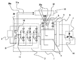
図1は、この発明の実施の形態1による電力変換装置の構成を示す図である。電力変換装置は、主回路である三相インバータ回路1と出力制御装置13とを備える。三相インバータ回路1は、第1の直流電源2からの直流電力を三相交流電力に変換して負荷7に出力するもので、第1の直流電源2は、アースとの間に浮遊静電容量17を持つ太陽電池などの直流電源である。負荷7は負荷接地点16で接地される。
三相インバータ回路1は、第1の直流電源2の電圧を母線電圧とする三相3レベルインバータ3と、三相3レベルインバータ3の各相交流出力線にそれぞれ直列接続された単相インバータ4と、単相インバータ4の後段に接続され、図示しないリアクトルおよびコンデンサから成る三相の平滑フィルタ6とを備える。
Hereinafter, a power converter according to
1 is a diagram showing a configuration of a power conversion device according to
The three-
三相3レベルインバータ3の各相は、それぞれダイオードが逆並列接続されたIGBT等から成る半導体スイッチング素子8を4個と、2個のクランプダイオード9とから構成される。また、三相3レベルインバータ3は、第1の直流電源2を分圧する2直列のコンデンサとして、第1の直列コンデンサ10、第2の直列コンデンサ11を備え、第1の直列コンデンサ10と第2の直列コンデンサ11との接続点が、各相の2個のクランプダイオード9の接続点に接続される。即ち、第1の直列コンデンサ10と第2の直列コンデンサ11との接続点は、第1の直流電源2の電圧を2分割する電位点である中性点となり、各相の上下各アームを構成する2つの半導体スイッチング素子8の接続点が中性点電位にクランプされる。
Each phase of the three-phase three-
各単相インバータ4は、4個の半導体スイッチング素子から成るフルブリッジインバータ12と、電圧を保持する第2の直流電源としての直流コンデンサ5とを備える。各相の単相インバータ4の出力電圧は、三相3レベルインバータ3の各相の出力電圧に重畳され、三相3レベルインバータ3の出力電圧と各単相インバータ4の出力電圧との電圧和を、平滑フィルタ6を介して負荷7に出力する。
なお、各単相インバータ4の直流コンデンサ5の電圧は、第1の直流電源2の電圧の1/2(あるいは第1、第2の直列コンデンサ10、11の電圧)に比べて小さく設定されている。即ち、直流コンデンサ5の電圧は、三相3レベルインバータ3の1レベルの電圧より小さい。また、図1では、便宜上、3つの各単相インバータ4の内、1相のみの回路構成を図示し他の相を省略した。
三相3レベルインバータ3および各単相インバータ4は、CPUやDSP、FPGAなどによる演算が可能な出力制御装置13から出力される三相3レベルインバータ制御信号14、単相インバータ制御信号15により駆動制御される。Each single-phase inverter 4 includes a full-
The voltage of the
The three-phase three-
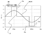
このように構成される三相インバータ回路1の動作を、図2〜図5に示す電圧波形に基づいて以下に説明する。波形の電位は、第1の直列コンデンサ10と第2の直列コンデンサ11との接続点である中性点を基準とした電位である。
図2に、三相インバータ回路1が出力する1相分、例えばU相の電圧指令である相電圧指令20と、三相3レベルインバータ3のU相が出力する電圧波形(三相3レベルインバータ電圧21)とを示す。なお、相電圧指令20は、各相が2π/3ずつ異なる位相で、同じ波高値を有する正弦波である。
第1の直流電源2により出力される直流電圧は、第1の直列コンデンサ10と第2の直列コンデンサ11との直列体に充電される。第1の直流電源2、第1の直列コンデンサ10、および第2の直列コンデンサ11の電圧は検出され、各検出電圧値は出力制御装置13へ伝送される。The operation of the three-
FIG. 2 shows a voltage waveform (three-phase three-level inverter) output by one phase output from the three-
The DC voltage output from the first
出力制御装置13からの三相3レベルインバータ制御信号14により、三相3レベルインバータ3の各相は、第1の直列コンデンサ10および第2の直列コンデンサ11の直流電圧を入力電圧とし、第1の直列コンデンサ10の電圧値、第2の直列コンデンサ11の電圧値の各電圧値(あるいは第1の直流電源2の電圧の1/2の電圧値)に相当する波高値、この場合200Vの電圧パルスを、相電圧指令20に対して半周期に1パルスの割合で出力する。この半周期に1パルスの電圧パルスを、以下、主電圧パルス21aと称す。ここでは、相電圧指令20の1周期に、該相電圧指令20の正側に1パルス、負側に1パルスの主電圧パルス21aを出力する。この主電圧パルス21aは、単相インバータ4の半周期(あるいは1周期)の電力収支が0となるように出力されるが、この制御についての詳細は後述する。
By the three-phase three-level inverter control signal 14 from the
図3に、単相インバータ4の出力電圧指令(単相インバータ電圧指令22)を示す。この単相インバータ電圧指令22は、三相インバータ回路1の相電圧指令20から各相の三相3レベルインバータ電圧21を減算して得られる。各単相インバータ4は、出力制御装置13からの単相インバータ制御信号15により、三相インバータ回路1に要求される相電圧指令20と三相3レベルインバータ3の各相の出力電圧との差を補うように高周波PWM制御されて出力する。また各単相インバータ4は、このPWM制御において、負荷7への各相出力電流が正弦波となるように制御される。
図4は、各相の単相インバータ4の単相インバータ電圧指令を示し、22aはU相単相インバータ電圧指令、22bはV相単相インバータ電圧指令、22cはW相単相インバータ電圧指令である。この場合、波形ピーク値は±125Vであり、この電圧指令の電圧を出力するためには各単相インバータ4の母線電圧は125V以上必要になる。FIG. 3 shows an output voltage command (single-phase inverter voltage command 22) of the single-phase inverter 4. This single-phase
FIG. 4 shows a single-phase inverter voltage command of the single-phase inverter 4 for each phase, 22a is a U-phase single-phase inverter voltage command, 22b is a V-phase single-phase inverter voltage command, and 22c is a W-phase single-phase inverter voltage command. is there. In this case, the waveform peak value is ± 125 V, and the bus voltage of each single-phase inverter 4 is required to be 125 V or more in order to output the voltage command voltage.
各相の単相インバータ4の出力電圧は、三相3レベルインバータ3の各相の出力電圧に重畳され、三相3レベルインバータ3の出力電圧と各単相インバータ4の出力電圧との電圧和を、平滑フィルタ6を介して負荷7に出力する。図5に、三相3レベルインバータ3の出力電圧と各単相インバータ4の出力電圧との電圧和である三相インバータ回路1の各相出力電圧を示す。23は各相出力電圧、24は各相出力電圧23の平均の電圧波形を示す。
負荷7への各相出力電圧波形24は、各相の相電圧指令20と同様の電圧波形となり、即ち、第1の直列コンデンサ10と第2の直列コンデンサ11との接続点である中性点の電位を基準に、各相が2π/3ずつ異なる位相で、同じ波高値を有する正弦波となる。The output voltage of the single-phase inverter 4 of each phase is superimposed on the output voltage of each phase of the three-phase three-
Each phase
次に、三相3レベルインバータ3の主電圧パルス21aの出力制御および単相インバータ4の電力収支について、図2を参照して以下に説明する。
上述したように、主電圧パルス21aは、単相インバータ4の半周期あるいは1周期の電力収支が0となるように出力される。相電圧指令20と三相3レベルインバータ3の各相の出力電圧との差を補うように単相インバータ4は出力するため、三相3レベルインバータ3は、相電圧指令20により出力される電力と同等の電力を主電圧パルス21aにより出力すれば良い。
出力電流の位相を出力電圧の位相に一致するよう制御する(力率1運転)場合、相電圧指令20のピーク電圧をVp、三相インバータ回路1に入力する直流電圧(ここでは、第1の直流電源2の電圧、あるいは、第1の直列コンデンサ10の電圧と第2の直列コンデンサ11の電圧との和)の1/2をEdとすると、Vpは次の式(1)で表せる。但し、θ1(0<θ1<π/2)は主電圧パルス21aが立ち上がる位相である。Next, the output control of the
As described above, the
When controlling the phase of the output current to match the phase of the output voltage (

上記式(1)から、主電圧パルス21aが立ち上がる位相θ1は、以下の式(2)となる。
From the above equation (1), the phase θ1 at which the
この様に演算される位相(nπ+θ1)で立ち上がるパルス幅が(π−2θ1)の電圧パルスが、主電圧パルス21aとなる。出力制御装置13では、以上の演算を行い、演算結果を基にした三相3レベルインバータ制御信号14を三相3レベルインバータ3へ送り、三相3レベルインバータ3を出力制御する。なお、上記演算では主電圧パルス21aが立ち上がる位相θ1を演算したが、この位相θ1を決定することは、パルス幅(π−2θ1)を決定することと同じである。
A voltage pulse having a pulse width of (π−2θ1) rising at the phase (nπ + θ1) calculated in this way becomes the
この実施の形態では、第1の直流電源2に接続するインバータに三相3レベルインバータ3を用い、三相インバータ回路1全体を、第1の直列コンデンサ10と第2の直列コンデンサ11との接続点である中性点の電位を基準に、各相が2π/3ずつ異なる位相で、同じ波高値を有する正弦波となるように制御した。このような構成では、中性点電位が安定となり第1の直流電源2の母線電位の変動が無く、所望の電圧波形が得られる出力電圧制御が高精度に実現でき、三相の出力電圧合計が0に成る。このため、三相出力の中性電位と第1の直流電源2の一方の電位との間に交流成分を持たず、第1の直流電源2の浮遊静電容量17を介して流れる零相電流を抑制できる。零相電流は、通常、負荷7の前段に配設される漏電遮断器に漏電電流として検出されるが、零相電流を抑制できるため漏電遮断器の誤作動を防止できると共に、漏電電流が低減できるため三相インバータ回路1の電力変換効率が向上する。
In this embodiment, a three-phase three-
また、三相インバータ回路1は、三相3レベルインバータ3の出力電圧と各単相インバータ4の出力電圧との和による電圧を出力するため、三相インバータ回路1の直流入力電圧である第1の直流電源2の電圧よりも高い電圧を出力できる。また、三相3レベルインバータ3の各相は、半周期で1パルス運転が為されるため、スイッチング損失がほとんど発生しない。高周波でPWM制御される単相インバータ4の直流電圧は、比較的小さな値に選定されているので、PWM制御によるスイッチング損失が小さく、平滑フィルタ6の容量も小さいものでよい。このため、三相インバータ回路1は、小型で低コストで、しかも変換効率の高い装置構成となる。
Further, since the three-
また、この実施の形態では、各単相インバータ4の半周期あるいは1周期の電力収支が0となるように三相インバータ回路1が制御されるため、各単相インバータ4の直流コンデンサ5は外部から電力授受する直流電源を持たない簡便な構成にできる。
In this embodiment, since the three-
実施の形態2.
上記実施の形態1では、三相3レベルインバータ3は、相電圧指令20により出力される電力と同等の電力を主電圧パルス21aにより出力するように、主電圧パルス21aのパルス幅(あるいは立ち上がり位相)を決定したが、他の手法でパルス幅を決定することもできる。この実施の形態では、単相インバータ4の半周期あるいは1周期の電力積算値を演算して、その電力積算値が0となるように主電圧パルス21aのパルス幅を求める。
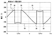
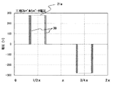
三相3レベルインバータ3の主電圧パルス21aのパルス幅と、単相インバータ4の出力電力との関係を、図6、図7に基づいて以下に説明する。図6は、単相インバータ4の半周期の電力積算値が正となる比較例の場合で、図7は、図6の場合より主電圧パルス21aのパルス幅を拡げ、単相インバータ4の半周期の電力積算値を0とした場合を示す。なお、便宜上、半周期の波形のみを図示している。
In the first embodiment, the three-phase, three-
The relationship between the pulse width of the
図6(a)、図7(a)に示すように、三相インバータ回路1の各相出力電圧波形24に対して、三相3レベルインバータ3は半周期に1パルスの主電圧パルス21aを出力する。
そして、図6(b)、図7(b)に示すように、三相3レベルインバータ3の主電圧パルス21aと各相出力電圧波形24との差の電圧波形が得られるように、単相インバータ4はPWM制御により平均的な電圧22dを出力する。例えば、三相3レベルインバータ3が太陽光パワーコンデショナの場合、負荷7への出力電流は力率1の場合が多い。力率1の場合、出力電流25の電流波形は、各相出力電圧波形24と同じ位相の正弦波となる。As shown in FIGS. 6A and 7A, for each phase
Then, as shown in FIGS. 6 (b) and 7 (b), a single phase is obtained so that a voltage waveform of the difference between the
そして、出力電圧22dと出力電流25との積である単相インバータ4の出力電力26は、図6(c)、図7(c)に示す波形となる。図6(c)では、単相インバータ4の出力電力26の半周期の積算値は正となるため、単相インバータ4の直流コンデンサ5には外部に電源が必要となる。図7(c)では、主電圧パルス21aのパルス幅を拡げ、この場合、単相インバータ4の負の出力電力26が増加し、半周期の電力積算値がゼロとなる。
The
この実施の形態では、単相インバータ4の半周期あるいは1周期の電力積算値が0となるように主電圧パルス21aのパルス幅を決定する。各単相インバータ4の半周期あるいは1周期の電力収支が0となるように制御されるため、各単相インバータ4の直流コンデンサ5は外部から電力授受する直流電源を持たない簡便な構成にできる。
In this embodiment, the pulse width of the
実施の形態3.
上記実施の形態1、2では、単相インバータ4の半周期あるいは1周期の電力収支が0となるように主電圧パルス21aのパルス幅を決定した。この実施の形態では、主電圧パルス21aのパルス幅を微調整するものを示す。この場合、各単相インバータ4の各直流コンデンサ5の電圧を測定するために各電圧検出器32(図10参照)を備える。
まず、上記実施の形態1、2と同様に、単相インバータ4の半周期あるいは1周期の電力収支が0となるように主電圧パルス21aのパルス幅を決定して三相インバータ回路1を出力制御する。この出力制御において、何らかの原因、例えば入力直流電圧の急変や、負荷7の急変等で単相インバータ4の電力収支のバランスが崩れると、単相インバータ4の直流コンデンサ5の電圧が変動する。
In the first and second embodiments, the pulse width of the
First, similarly to the first and second embodiments, the three-
各電圧検出器32は各単相インバータ4の各直流コンデンサ5の電圧を検出し、検出された各直流コンデンサ5の電圧値は出力制御装置13に伝送される。出力制御装置13では、直流コンデンサ5の電圧値が予め設定された基準値よりも大きい時は、対応する相の主電圧パルス21aのパルス幅を短くし、基準値よりも大きい時はパルス幅を長くして、直流コンデンサ5の電圧値が基準値に近づくように三相3レベルインバータ3を制御する。
Each
上記実施の形態2で説明したように、単相インバータ4の半周期あるいは1周期の電力積算値は、主電圧パルス21aのパルス幅を短くすると増大し、主電圧パルス21aのパルス幅を長くすると低減する。このため、直流コンデンサ5の電圧値が基準値よりも大きい時、対応する相の主電圧パルス21aのパルス幅を短くすることで、単相インバータ4の電力積算値を増大させて直流コンデンサ5の電圧を小さくする。また、直流コンデンサ5の電圧値が基準値よりも小さい時、対応する相の主電圧パルス21aのパルス幅を長くすることで、単相インバータ4の電力積算値を低減させて直流コンデンサ5の電圧を大きくする。
As described in the second embodiment, the half-cycle or one-cycle power integrated value of the single-phase inverter 4 increases when the pulse width of the
このように、三相3レベルインバータ3が出力する主電圧パルス21aのパルス幅を調整することで、各単相インバータ4の直流コンデンサ5の電圧が基準値となるようにフィードバック制御する。これにより、各単相インバータ4の半周期あるいは1周期の電力収支が確実に0に制御できる。このため、単相インバータ4の出力電圧不足や、直流コンデンサ5の過充電、および過充電による単相インバータ4の絶縁破壊などを防ぐことができ、安定した出力の三相インバータ回路1を得ることができる。
In this way, feedback control is performed so that the voltage of the
実施の形態4.
次に、この発明の実施の形態4による電力変換装置を図に基づいて説明する。
図8は、この発明の実施の形態4による電力変換装置の構成を示す図である。この実施の形態の三相インバータ回路1では、三相3レベルインバータ3の各相交流出力線にそれぞれ複数台(この場合2台)の単相インバータ4、4aを直列接続する。各相2台の単相インバータ4、4aは、同様の構成であり、便宜上、1つの単相インバータ4のみ回路構成を図示し、他を省略した。
そして、三相3レベルインバータ3および各単相インバータ4、4aは、CPUやDSP、FPGAなどによる演算が可能な出力制御装置13aから出力される三相3レベルインバータ制御信号14、単相インバータ制御信号15、15aにより駆動制御される。
その他の構成は、上記実施の形態1の図1で示した構成と同様である。Embodiment 4 FIG.
Next, a power converter according to Embodiment 4 of the present invention will be described with reference to the drawings.
FIG. 8 is a diagram showing a configuration of a power conversion device according to Embodiment 4 of the present invention. In the three-
The three-phase three-
Other configurations are the same as those shown in FIG. 1 of the first embodiment.
次に、動作について説明する。
三相3レベルインバータ3の各相は、上記実施の形態1と同様に、相電圧指令20に対して半周期に1パルスの割合で主電圧パルス21aを出力する。この主電圧パルス21aは、単相インバータ4の半周期(あるいは1周期)の電力収支が0となるようにパルス幅が決定されて出力される。
各単相インバータ4、4aは、三相インバータ回路1に要求される相電圧指令20と三相3レベルインバータ3の各相の出力電圧との差を補うように高周波PWM制御されて出力する。この場合、各相において2台の単相インバータ4、4aの出力電圧の和で、相電圧指令20と三相3レベルインバータ3の各相の出力電圧との差を補う。また各単相インバータ4、4aは、このPWM制御において出力電流が正弦波となるように制御される。Next, the operation will be described.
Each phase of the three-phase three-
Each single-
各相の2台の単相インバータ4、4aの出力電圧は、三相3レベルインバータ3の各相の出力電圧に重畳され、三相3レベルインバータ3の出力電圧と各単相インバータ4、4aの出力電圧との電圧和を、平滑フィルタ6を介して負荷7に出力する。
図9に、三相3レベルインバータ3の出力電圧と2台の単相インバータ4、4aの出力電圧との電圧和である三相インバータ回路1の各相出力電圧を示す。23aは各相出力電圧、24は各相出力電圧23の平均の電圧波形を示す。この場合、直列接続された2台の単相インバータ4、4aは、例えばキャリア波の位相を180°ずらすことによりスイッチングのタイミングをずらして出力している。
負荷7への各相出力電圧波形24は、上記実施の形態1と同様に、各相の相電圧指令20と同様の電圧波形となり、即ち、第1の直列コンデンサ10と第2の直列コンデンサ11との接続点である中性点の電位を基準に、各相が2π/3ずつ異なる位相で、同じ波高値を有する正弦波となる。The output voltage of the two single-
FIG. 9 shows each phase output voltage of the three-
Similarly to the first embodiment, each phase
この実施の形態においても、上記実施の形態1と同様に、中性点電位が安定となり第1の直流電源2の母線電位の変動が無く、所望の電圧波形が得られる出力電圧制御が高精度に実現でき、三相の出力電圧合計が0に成る。このため、三相出力の中性電位と第1の直流電源2の一方の電位との間に交流成分を持たず、第1の直流電源2の浮遊静電容量17を介して流れる零相電流を抑制できる。
また、三相3レベルインバータ3の各相交流出力線にそれぞれ複数台(この場合2台)の単相インバータ4、4aを直列接続するため、各単相インバータ4、4aが出力する電圧を低減でき、スイッチング損失が低減する。また、単相インバータ4、4aの直列数を増加するとキャリア波の周波数を下げてもよく、さらにスイッチング損失が低減する。Also in this embodiment, as in the first embodiment, the neutral point potential is stable, the bus potential of the first
In addition, since a plurality of (two in this case) single-
なお、直列接続した2台の単相インバータ4、4aの内、1台の単相インバータ4は半周期で数パルス以下の出力で、他の単相インバータ4aのみ高周波PWM制御して出力してもよい。この時、PWM制御する単相インバータ4aの直流電圧を単相インバータ4の直流電圧より低くしても良い。
Of the two single-
実施の形態5.
次に、この発明の実施の形態5による電力変換装置を図に基づいて説明する。
図10は、この発明の実施の形態5による電力変換装置の構成を示す図である。この実施の形態では、第1の直列コンデンサ10の電圧を測定するために並列に設けられた電圧検出器30と、第2の直列コンデンサ11の電圧を測定するために並列に設けられた電圧検出器31と、各単相インバータ4の各直流コンデンサ5の電圧を測定するために設けられた各電圧検出器32とを備える。これらの電圧検出器30〜32にて検出された電圧値30a〜32aは、出力制御装置13に伝送され、出力制御装置13は検出された電圧値30a〜32aに基づいて、三相3レベルインバータ3および各単相インバータ4を制御する。
その他の構成は、上記実施の形態1の図1で示した構成と同様である。
Next, a power converter according to
FIG. 10 is a diagram showing a configuration of a power conversion device according to
Other configurations are the same as those shown in FIG. 1 of the first embodiment.
上記実施の形態1では、三相3レベルインバータ3は半周期で1パルスの主電圧パルス21aのみを出力するものであったが、この実施の形態5では、三相3レベルインバータ3が異なる動作をする。図11〜図14は、実施の形態5による三相インバータ回路1の動作を説明するための電圧波形を示した図である。波形の電位は、第1の直列コンデンサ10と第2の直列コンデンサ11との接続点である中性点を基準とした電位である。なお、図11、図12は、比較例を示し、図13、図14は実施の形態5による三相インバータ回路1の電圧波形である。
In the first embodiment, the three-phase three-
仮に、上記実施の形態1と同様に動作した場合、三相インバータ回路1の相電圧指令20(各相出力電圧波形24)と、三相3レベルインバータ3の各相が出力する電圧波形(三相3レベルインバータ電圧21)とを図11に示す。相電圧指令20の正側に出力される主電圧パルス21aの電圧は、第1の直列コンデンサ10の電圧値30aであり、相電圧指令20の負側に出力される主電圧パルス21aの電圧(絶対値)は、第2の直列コンデンサ11の電圧値31aである。この場合、図2で示した通常の場合より、第1の直流電源2の電圧が高くなり、第1、第2の直列コンデンサ10、11の電圧値30a、31aが高くなった場合を示している。
上述したように、主電圧パルス21aのパルス幅は、単相インバータ4の半周期あるいは1周期の電力収支が0に成るように決定されるため、三相3レベルインバータ3の直流入力電圧が大きくなると、図に示すように、パルス幅は短くなる。If the operation is the same as in the first embodiment, the phase voltage command 20 (each phase output voltage waveform 24) of the three-
As described above, the pulse width of the
三相3レベルインバータ3の各相が、図11で示したような三相3レベルインバータ電圧21を出力する場合、単相インバータ4の出力電圧指令(単相インバータ電圧指令22)を図12に示す。この単相インバータ電圧指令22は、三相インバータ回路1の相電圧指令20から三相3レベルインバータ電圧21を減算して得られる。
単相インバータ4は、3相インバータ回路1の相電圧指令20と三相3レベルインバータ電圧21との差電圧を発生する必要があるが、この差電圧は、第1、第2の直列コンデンサ10、11の電圧値30a、31aが高くなって主電圧パルス21aのパルス幅が短くなると増大する。このため、図に示すように、主電圧パルス21aの立ち上がり部分の近傍および立下り部分の近傍の期間に、単相インバータ4の出力電圧限界値35を超える電圧36が要求される。なお、出力電圧限界値35の大きさは、単相インバータ4の直流コンデンサ5の電圧値32aである。When each phase of the three-phase three-
The single-phase inverter 4 needs to generate a difference voltage between the
図13は、この実施の形態による単相インバータ4の出力電圧指令(単相インバータ電圧指令37)を示す図であり、図14は、この実施の形態による三相3レベルインバータ3の各相が出力する電圧波形(三相3レベルインバータ電圧)を示す。
単相インバータ4は、図12で示したような出力電圧限界値35を超える電圧36を出力できないため、出力電圧限界値35を超える電圧36が要求される期間では、図14に示すように、単相インバータ4の出力電圧の不足分を三相3レベルインバータ3に負担させる。即ち、主電圧パルス21aの立ち上がり部分の近傍および立下り部分の近傍の期間に、三相3レベルインバータ3はPWM制御による電圧である部分PWM電圧38を出力して、単相インバータ4の出力電圧では不足する電圧分を出力する。FIG. 13 is a diagram showing an output voltage command (single-phase inverter voltage command 37) of the single-phase inverter 4 according to this embodiment, and FIG. 14 shows each phase of the three-phase three-
Since the single-phase inverter 4 cannot output the
なお、部分PWM電圧38は第1、第2の直列コンデンサ10、11の電圧値30a、31aおよび直流コンデンサ5の電圧値32aに応じて出力する。即ち、第1、第2の直列コンデンサ10、11の電圧がそれほど高くない、あるいは直流コンデンサ5の電圧が充分高いことにより、三相3レベルインバータ3の主電圧パルス21aと単相インバータ4の出力電圧との組み合わせのみで正弦波の電圧波形が得られる場合は、上記実施の形態1と同様の制御を採用し、必要な場合は、部分PWM電圧38を出力する制御に切り替える。
The
以上の様に、この実施の形態では、三相3レベルインバータ3の各相が半周期に1パルス出力する主電圧パルス21aの立ち上がり部分の近傍および立下り部分の近傍の期間に部分PWM電圧38を出力可能とした。このため、第1の直流電源2の電圧が増加して第1、第2の直列コンデンサ10、11の電圧が増加しても、相電圧指令20と同様の正弦波の電圧波形が得られる。このため中性点電位が安定となり第1の直流電源2の母線電位の変動が無く、所望の電圧波形がさらに安定して高精度に得られる。このため、第1の直流電源2の浮遊静電容量17を介して流れる零相電流の抑制が、安定して確実に実現できる。
As described above, in this embodiment, the
なお、上記実施の形態では、三相3レベルインバータ3が部分PWM電圧38を出力する期間として、単相インバータ4が出力電圧限界値35を超える電圧36を要求される期間と説明したが、実際には余裕を持たせて以下のように制御される。即ち、相電圧指令20(各相出力電圧波形)と、主電圧パルス21aのみから成る三相3レベルインバータ電圧21との差電圧の絶対値を、直流コンデンサ5の電圧値32aから減算した値が所定値以下となる期間に、部分PWM電圧38を出力する。これにより、相電圧指令20(各相出力電圧波形)と、主電圧パルス21aのみから成る三相3レベルインバータ電圧21との差電圧を、単相インバータ4から確実に出力可能となり、相電圧指令20と同様の正弦波の電圧波形が得られる。
In the above embodiment, the period in which the three-phase three-
また、この実施の形態においても、上記各単相インバータの半周期あるいは1周期の出力電力収支が0となるように、上記三相3レベルインバータ3が出力する主電圧パルス21aのパルス幅および部分PWM電圧38の出力期間は制御される。
Also in this embodiment, the pulse width and part of the
さらに、上記実施の形態3と同様に、三相3レベルインバータ3の電圧出力期間を微調整して、各単相インバータ4の直流コンデンサ5の電圧が基準値となるようにフィードバック制御しても良い。この場合、三相3レベルインバータ3の電圧出力期間は、主電圧パルス21aのパルス幅および部分PWM電圧38の出力期間から成り、直流コンデンサ5の電圧値が基準値よりも大きい時は、三相3レベルインバータ3の対応相の電圧出力期間を短くし、基準値よりも大きい時は電圧出力期間を長くする。
これにより、主電圧パルス21aのみの制御と部分PWM電圧38を発生させる制御との切り換え時などで、各単相インバータ4の半周期あるいは1周期の電力収支が0からずれた場合にも、速やかに0に戻す制御が可能になる。このため、単相インバータ4の出力電圧不足や、直流コンデンサ5の過充電、および過充電による単相インバータ4の絶縁破壊などを防ぐことができ、安定した出力の三相インバータ回路1を得ることができる。Further, as in the third embodiment, the voltage output period of the three-phase three-
Thus, even when the half-cycle or one-cycle power balance of each single-phase inverter 4 is deviated from 0, for example, when switching between the control of only the
実施の形態6.
次に、この発明の実施の形態6による電力変換装置を図に基づいて説明する。
図15は、この発明の実施の形態6による電力変換装置の構成を示す図である。この実施の形態では、三相インバータ回路1に第1の直流電源2の電圧を昇圧する昇圧回路40を設け、昇圧回路40の出力電圧を三相3レベルインバータ3の直流入力電圧とする。昇圧回路40は、例えば、リアクトル41、第1の直流電源2の高圧側母線と低圧側母線との間に接続されたスイッチ42、および一方向の電流を流して第1、第2の直列コンデンサ10、11を充電するダイオード43で構成される。
その他の構成は、上記実施の形態5の図10で示した構成と同様で、三相3レベルインバータ3と各単相インバータ4とは、上記実施の形態5と同様に制御される。
Next, a power converter according to
FIG. 15 is a diagram showing a configuration of a power conversion device according to
The other configuration is the same as that shown in FIG. 10 of the fifth embodiment, and the three-phase three-
第1の直流電源2が、例えば太陽電池のような自然エネルギを利用する電源の場合、気象変化等で出力電圧は常に変化する。太陽電池では、朝夕、曇りの時に出力電圧が低下する。三相3レベルインバータ3の出力可能な交流電圧は、三相3レベルインバータ3の母線電圧値である、第1の直列コンデンサ10の電圧値30aと第2の直列コンデンサ11の電圧値31aにより決まる。
図16は、第1の直流電源2の電圧と三相3レベルインバータ3が出力する主電圧パルス21aのパルス幅の関係を示す図である。負荷7への出力電圧は三相、200Vrmsとした。図16に示すように、第1の直流電源電圧が256.51Vより低い電圧の時、昇圧回路40により256.51Vまで昇圧する。第1の直流電源電圧が256.51V以上になると、主電圧パルス21aのパルス幅を短くし、362.7V以上になると部分PWM電圧38を出力する制御に切り替える。When the first
FIG. 16 is a diagram showing the relationship between the voltage of the first
この実施の形態では、昇圧回路40により第1の直流電源2の電圧を昇圧して、三相3レベルインバータ3の直流入力電圧となる第1の直列コンデンサ10の電圧値30aと第2の直列コンデンサ11の電圧値31aとを、所望の交流電圧が出力可能の電圧まで高くした。このため、第1の直流電源2が低い電圧から三相インバータ回路1の波形出力が可能になり、三相インバータ回路1の動作可能範囲が拡がる。
In this embodiment, the voltage of the first
なお、この実施の形態では、上記実施の形態5で示した制御を用いたが、上記実施の形態1〜4の各実施の形態を適用しても良い。 In this embodiment, the control shown in the fifth embodiment is used, but each of the first to fourth embodiments may be applied.
実施の形態7.
次に、この発明の実施の形態7による電力変換装置を図17に基づいて説明する。
図17に示すように、三相インバータ回路1の各相出力と負荷7との間に、三相インバータ回路1が出力する電荷量以上の静電容量を持つコンデンサ44を直列接続して備え、第1の直流電源2の出力端子の低圧側が接地点45でアースに接地される。その他の構成は上記実施の形態1の図1で示した構成と同様であるが、他の上記各実施の形態に適用しても良い。
Next, a power converter according to
As shown in FIG. 17, a
第1の直流電源2を接地した場合、三相インバータ回路1の各相の出力電圧は、第1の直流電源2の電圧の1/2の電圧値、あるいは第2の直列コンデンサ11の電圧値を中性点電位として出力するため、その直流電圧分だけ加算された波形を出力する。この実施の形態では、各相にコンデンサ44を備えたため、これらのコンデンサ44が直流成分をカットして、交流成分だけを負荷7に出力する。このように負荷7へ出力される直流電圧成分を遮断するため、負荷7となる系統に出力して系統に連系できる。
When the first
実施の形態8.
次に、この発明の実施の形態8による電力変換装置を図18に基づいて説明する。
図18に示すように、三相インバータ回路1と負荷7との間に、絶縁が可能な絶縁トランス46を配置し、第1の直流電源2の出力端子の低圧側が接地点45でアースに接地される。この絶縁トランス46は巻き数比による一般的な昇圧機能を備えてもよい。この場合、零相電流経路は絶縁トランス46により遮断されるため、零相電流は流れない。
第1の直流電源2を接地した場合、三相インバータ回路1の各相の出力電圧は、第1の直流電源2の電圧の1/2の電圧値、あるいは第2の直列コンデンサ11の電圧値を中性点電位として出力するため、その直流電圧分だけ加算された波形を出力する。この実施の形態では、絶縁トランス46を備えたため、絶縁トランス46により直流成分がカットされ、交流成分だけを負荷7に出力する。このように負荷7へ出力される直流電圧成分を遮断するため、負荷7となる系統に出力して系統に連系できる。また、絶縁トランス46で昇圧すると、高い交流電圧が出力可能になる。
Next, a power conversion device according to
As shown in FIG. 18, an insulating
When the first
Claims (8)
上記三相3レベルインバータの出力電圧と上記各単相インバータの出力電圧との総和を平滑フィルタを介して負荷に出力するものであり、
上記単相インバータの直流入力電源である第2の直流電源を直流コンデンサにて構成し、該第2の直流電源の電圧は、上記三相3レベルインバータの1レベルの電圧より小さく、
上記制御装置は、
上記三相3レベルインバータの各相が上記負荷への各相出力電圧の半周期に対して1パルスの電圧を主電圧パルスとして出力するように上記三相3レベルインバータを制御すると共に、上記各単相インバータの半周期あるいは1周期の出力電力収支が0となるように、上記三相3レベルインバータが出力する上記主電圧パルスのパルス幅を制御し、
上記各単相インバータをPWM制御して、
上記負荷への各相出力電圧を、上記第1の直流電源の基準電位からゼロあるいは一定の直流電位を有した点を基準とし、各相が2π/3ずつ異なる位相で同じ波高値を有する正弦波になるよう制御するものであって、
上記各単相インバータの上記第2の直流電源の電圧値が基準値よりも大きい時は対応する相の上記主電圧パルスのパルス幅を短くし、上記第2の直流電源の電圧値が基準値よりも小さい時は対応する相の上記主電圧パルスのパルス幅を長くする、
ことを特徴とする電力変換装置。A three-phase three-level inverter connected between the positive and negative terminals of the first DC power source, a single-phase inverter connected in series to each phase AC output line of the three-phase three-level inverter, respectively, and a control device; Prepared,
The sum of the output voltage of the three-phase three-level inverter and the output voltage of each single-phase inverter is output to a load through a smoothing filter,
A second DC power supply, which is a DC input power supply for the single-phase inverter, is constituted by a DC capacitor, and the voltage of the second DC power supply is smaller than the one-level voltage of the three-phase three-level inverter,
The control device
The three-phase three-level inverter controls the three-phase three-level inverter so that each phase of the three-phase three-level inverter outputs one pulse voltage as a main voltage pulse with respect to a half cycle of each phase output voltage to the load. The pulse width of the main voltage pulse output from the three-phase three-level inverter is controlled so that the half-cycle or single-cycle output power balance of the single-phase inverter is zero.
PWM control of each single-phase inverter,
Each phase output voltage to the load is a sine with each phase having the same peak value with a phase different by 2π / 3 with reference to the point having zero or constant DC potential from the reference potential of the first DC power source. To control it to become a wave ,
When the voltage value of the second DC power supply of each single-phase inverter is larger than the reference value, the pulse width of the main voltage pulse of the corresponding phase is shortened, and the voltage value of the second DC power supply is the reference value. When smaller than, increase the pulse width of the main voltage pulse of the corresponding phase,
The power converter characterized by the above-mentioned.
上記三相3レベルインバータの出力電圧と上記各単相インバータの出力電圧との総和を平滑フィルタを介して負荷に出力するものであり、 The sum of the output voltage of the three-phase three-level inverter and the output voltage of each single-phase inverter is output to a load through a smoothing filter,
上記単相インバータの直流入力電源である第2の直流電源を直流コンデンサにて構成し、該第2の直流電源の電圧は、上記三相3レベルインバータの1レベルの電圧より小さく、 A second DC power supply, which is a DC input power supply for the single-phase inverter, is constituted by a DC capacitor, and the voltage of the second DC power supply is smaller than the one-level voltage of the three-phase three-level inverter,
上記制御装置は、 The control device
上記三相3レベルインバータの各相が、上記負荷への各相出力電圧の半周期に対して1パルスの主電圧パルスと、該主電圧パルスの立ち上がり部分近傍および立下り部分近傍にPWM制御による多パルスとを出力するように、上記三相3レベルインバータを制御すると共に、上記各単相インバータの半周期あるいは1周期の出力電力収支が0となるように、上記三相3レベルインバータが出力する上記主電圧パルスのパルス幅および上記PWM制御による電圧出力期間を制御し、 Each phase of the three-phase three-level inverter is controlled by PWM control in the vicinity of one main voltage pulse in the half cycle of each phase output voltage to the load and the rising and falling portions of the main voltage pulse. The three-phase three-level inverter controls the three-phase three-level inverter so that multiple pulses are output, and the three-phase three-level inverter outputs so that the half-cycle or one-cycle output power balance of each single-phase inverter becomes zero. Controlling the pulse width of the main voltage pulse and the voltage output period by the PWM control,
上記各単相インバータをPWM制御して、 PWM control of each single-phase inverter,
上記負荷への各相出力電圧を、上記第1の直流電源の基準電位からゼロあるいは一定の直流電位を有した点を基準とし、各相が2π/3ずつ異なる位相で同じ波高値を有する正弦波になるよう制御するものであって、 Each phase output voltage to the load is a sine with each phase having the same peak value with a phase different by 2π / 3 with reference to the point having zero or constant DC potential from the reference potential of the first DC power source. To control it to become a wave,
上記各単相インバータの上記第2の直流電源の電圧値が基準値よりも大きい時は対応する相の上記三相3レベルインバータの電圧出力期間を短くし、上記第2の直流電源の電圧値が基準値よりも小さい時は対応する相の上記三相3レベルインバータの電圧出力期間を長くする、 When the voltage value of the second DC power supply of each single-phase inverter is larger than a reference value, the voltage output period of the three-phase three-level inverter of the corresponding phase is shortened, and the voltage value of the second DC power supply When is smaller than the reference value, the voltage output period of the three-phase three-level inverter of the corresponding phase is lengthened.
ことを特徴とする電力変換装置。 The power converter characterized by the above-mentioned.
上記三相3レベルインバータは、上記2直列のコンデンサの中間点に電位を固定するクランプダイオードを備えた中性点クランプ式インバータであることを特徴とする請求項1から請求項3のいずれか1項に記載の電力変換装置。A two-series capacitor for dividing the voltage of the first DC power supply, which is a DC input of the three-phase three-level inverter,
4. The neutral point clamp type inverter provided with a clamp diode that fixes a potential at an intermediate point of the two series capacitors, wherein the three-phase three-level inverter is any one of claims 1 to 3. The power converter according to item .
Priority Applications (1)
| Application Number | Priority Date | Filing Date | Title |
|---|---|---|---|
| JP2010539128A JP5097828B2 (en) | 2008-11-18 | 2009-11-11 | Power converter |
Applications Claiming Priority (4)
| Application Number | Priority Date | Filing Date | Title |
|---|---|---|---|
| JP2008294257 | 2008-11-18 | ||
| JP2008294257 | 2008-11-18 | ||
| JP2010539128A JP5097828B2 (en) | 2008-11-18 | 2009-11-11 | Power converter |
| PCT/JP2009/006015 WO2010058536A1 (en) | 2008-11-18 | 2009-11-11 | Power conversion device |
Publications (2)
| Publication Number | Publication Date |
|---|---|
| JPWO2010058536A1 JPWO2010058536A1 (en) | 2012-04-19 |
| JP5097828B2 true JP5097828B2 (en) | 2012-12-12 |
Family
ID=42197979
Family Applications (1)
| Application Number | Title | Priority Date | Filing Date |
|---|---|---|---|
| JP2010539128A Expired - Fee Related JP5097828B2 (en) | 2008-11-18 | 2009-11-11 | Power converter |
Country Status (5)
| Country | Link |
|---|---|
| US (1) | US8625307B2 (en) |
| EP (1) | EP2357721B1 (en) |
| JP (1) | JP5097828B2 (en) |
| CN (1) | CN102217182B (en) |
| WO (1) | WO2010058536A1 (en) |
Families Citing this family (39)
| Publication number | Priority date | Publication date | Assignee | Title |
|---|---|---|---|---|
| JP5374336B2 (en) * | 2009-12-01 | 2013-12-25 | 三菱電機株式会社 | Power converter |
| CN102918758B (en) * | 2010-05-28 | 2015-03-18 | 三菱电机株式会社 | Power conversion device |
| JP5478367B2 (en) * | 2010-05-31 | 2014-04-23 | 三菱電機株式会社 | Power converter |
| CN101881801B (en) * | 2010-07-21 | 2012-07-11 | 上海正泰电源系统有限公司 | Photovoltaic inverter leakage current detection method |
| JP5645209B2 (en) * | 2011-10-14 | 2014-12-24 | 三菱電機株式会社 | Power converter |
| IN2014CN04730A (en) * | 2011-11-30 | 2015-09-18 | Panasonic Corp | |
| US9007789B2 (en) * | 2011-12-12 | 2015-04-14 | Chen Na | Electric circuit for high voltage power conversion |
| CN102545681B (en) * | 2012-01-18 | 2014-04-23 | 南京航空航天大学 | Step wave synthesis three-phase inverter capable of eliminating low frequency harmonic waves and control method |
| JP2013158093A (en) * | 2012-01-27 | 2013-08-15 | Fuji Electric Co Ltd | Three-level power conversion device |
| CN104247246B (en) * | 2012-04-26 | 2017-07-28 | 三菱电机株式会社 | Power model and the three-level power conversion device using the power model |
| DK2672624T3 (en) * | 2012-06-05 | 2014-12-01 | Siemens Ag | Power regulator and generator system |
| US8730696B2 (en) * | 2012-07-16 | 2014-05-20 | Delta Electronics, Inc. | Multi-level voltage converter |
| CN104718692B (en) | 2012-10-17 | 2017-04-26 | 株式会社村田制作所 | Inverter device |
| US9595887B2 (en) * | 2013-02-15 | 2017-03-14 | Mitsubishi Electric Corporation | Three-phase power conversion device |
| JP6079407B2 (en) * | 2013-04-22 | 2017-02-15 | 富士電機株式会社 | Multi-level conversion circuit |
| JP6176121B2 (en) * | 2014-01-10 | 2017-08-09 | 住友電気工業株式会社 | Power converter and three-phase AC power supply |
| JP6252816B2 (en) * | 2014-08-25 | 2017-12-27 | 富士電機株式会社 | Power converter |
| JP6426462B2 (en) * | 2014-12-24 | 2018-11-21 | 株式会社東芝 | Power converter and control method thereof |
| CN104578886B (en) * | 2015-01-23 | 2017-06-13 | 阳光电源股份有限公司 | A kind of three-level photovoltaic inverter pulse duration modulation method and modulator |
| TWI547088B (en) * | 2015-01-29 | 2016-08-21 | 台達電子工業股份有限公司 | Dc-to-ac conversion apparatus and method of operating the same |
| EP3258338B1 (en) * | 2015-02-10 | 2021-06-16 | Kabushiki Kaisha Toshiba, Aka Toshiba Corporation | Control device for power conversion apparatus, control program, and power conversion apparatus |
| EP3316470B1 (en) * | 2015-06-23 | 2019-12-25 | Nissan Motor Co., Ltd. | Inverter with charging capability |
| US9742311B2 (en) | 2015-10-02 | 2017-08-22 | Hamilton Sundstrand Corporation | Systems and methods for controlling inverters |
| JP6753137B2 (en) * | 2016-05-12 | 2020-09-09 | 富士電機株式会社 | Boost chopper circuit |
| WO2018061184A1 (en) * | 2016-09-30 | 2018-04-05 | 東芝三菱電機産業システム株式会社 | Uninterruptible power supply unit |
| JP6851895B2 (en) * | 2017-04-26 | 2021-03-31 | 株式会社東芝 | Power converter |
| JP6390806B1 (en) * | 2017-08-02 | 2018-09-19 | 株式会社明電舎 | Inverter device |
| US10491138B1 (en) * | 2019-02-07 | 2019-11-26 | Hamilton Sundstrand Corporation | Multilevel inverters and methods of controlling multilevel inverters |
| US10516347B1 (en) * | 2019-03-27 | 2019-12-24 | Omron Automotive Electronics Co., Ltd. | Load detection method and apparatus |
| EP3975408A4 (en) * | 2019-05-23 | 2022-06-01 | Mitsubishi Electric Corporation | Power conversion device |
| JP7267287B2 (en) * | 2019-06-04 | 2023-05-01 | 東芝三菱電機産業システム株式会社 | Power conversion device and power conversion control device |
| JP6682049B1 (en) | 2019-06-25 | 2020-04-15 | 三菱電機株式会社 | Power converter |
| CN111371338A (en) * | 2020-04-14 | 2020-07-03 | 上海宝准电源科技有限公司 | Neutral point potential balance control strategy of self-adaptive NPC three-level converter |
| EP4195491A4 (en) * | 2020-08-04 | 2023-08-30 | Mitsubishi Electric Corporation | Electric power conversion device |
| WO2022180709A1 (en) | 2021-02-25 | 2022-09-01 | 三菱電機株式会社 | Power conversion device |
| JP7376548B2 (en) * | 2021-10-14 | 2023-11-08 | 本田技研工業株式会社 | Power conversion device, power conversion device control method, and program |
| JP7271808B1 (en) * | 2022-04-04 | 2023-05-11 | 三菱電機株式会社 | Power converters and flying objects |
| CN114670685A (en) * | 2022-04-20 | 2022-06-28 | 福州大学 | Single-phase vehicle-mounted integrated three-level NPC charging power supply module |
| CN115913002B (en) * | 2022-11-25 | 2023-10-13 | 江苏国科智能电气有限公司 | Three-level inverter of brushless direct current motor and control method thereof |
Citations (5)
| Publication number | Priority date | Publication date | Assignee | Title |
|---|---|---|---|---|
| JP2006081362A (en) * | 2004-09-13 | 2006-03-23 | Mitsubishi Electric Corp | Power converter |
| JP2007037355A (en) * | 2005-07-29 | 2007-02-08 | Mitsubishi Electric Corp | Power converter |
| JP2007169730A (en) * | 2005-12-22 | 2007-07-05 | Nippon Reliance Kk | Ac power supply device, and arc preventive method in the device |
| WO2008102552A1 (en) * | 2007-02-22 | 2008-08-28 | Mitsubishi Electric Corporation | Power conversion device |
| JP2008278560A (en) * | 2007-04-25 | 2008-11-13 | Toyota Motor Corp | Power supply controller, control method thereof, and computer readable recording medium recording program for making computer perform control method of power supply |
Family Cites Families (7)
| Publication number | Priority date | Publication date | Assignee | Title |
|---|---|---|---|---|
| JP2002165461A (en) | 2000-11-28 | 2002-06-07 | Meidensha Corp | Transformerless inverter power supply |
| JP4052195B2 (en) * | 2003-07-31 | 2008-02-27 | トヨタ自動車株式会社 | Voltage conversion device and computer-readable recording medium recording program for causing computer to execute control of voltage conversion |
| JP4506980B2 (en) * | 2004-02-03 | 2010-07-21 | トヨタ自動車株式会社 | Hybrid fuel cell system and voltage conversion control method thereof |
| CN101432957B (en) * | 2006-04-25 | 2012-10-03 | 三菱电机株式会社 | Power converting apparatus |
| JP2008092651A (en) | 2006-09-29 | 2008-04-17 | Mitsubishi Electric Corp | Power converter and power conversion system |
| US7785915B2 (en) | 2006-10-30 | 2010-08-31 | Aptina Imaging Corporation | Wafer level method of locating focal plane of imager devices |
| JP4898898B2 (en) | 2007-02-22 | 2012-03-21 | 三菱電機株式会社 | Three-phase power converter |
-
2009
- 2009-11-11 JP JP2010539128A patent/JP5097828B2/en not_active Expired - Fee Related
- 2009-11-11 WO PCT/JP2009/006015 patent/WO2010058536A1/en active Application Filing
- 2009-11-11 EP EP09827317.0A patent/EP2357721B1/en not_active Not-in-force
- 2009-11-11 US US13/127,132 patent/US8625307B2/en active Active
- 2009-11-11 CN CN200980146061.6A patent/CN102217182B/en not_active Expired - Fee Related
Patent Citations (5)
| Publication number | Priority date | Publication date | Assignee | Title |
|---|---|---|---|---|
| JP2006081362A (en) * | 2004-09-13 | 2006-03-23 | Mitsubishi Electric Corp | Power converter |
| JP2007037355A (en) * | 2005-07-29 | 2007-02-08 | Mitsubishi Electric Corp | Power converter |
| JP2007169730A (en) * | 2005-12-22 | 2007-07-05 | Nippon Reliance Kk | Ac power supply device, and arc preventive method in the device |
| WO2008102552A1 (en) * | 2007-02-22 | 2008-08-28 | Mitsubishi Electric Corporation | Power conversion device |
| JP2008278560A (en) * | 2007-04-25 | 2008-11-13 | Toyota Motor Corp | Power supply controller, control method thereof, and computer readable recording medium recording program for making computer perform control method of power supply |
Also Published As
| Publication number | Publication date |
|---|---|
| CN102217182B (en) | 2014-09-10 |
| CN102217182A (en) | 2011-10-12 |
| EP2357721A1 (en) | 2011-08-17 |
| EP2357721B1 (en) | 2016-03-30 |
| EP2357721A4 (en) | 2014-12-24 |
| JPWO2010058536A1 (en) | 2012-04-19 |
| WO2010058536A1 (en) | 2010-05-27 |
| US8625307B2 (en) | 2014-01-07 |
| US20110211381A1 (en) | 2011-09-01 |
Similar Documents
| Publication | Publication Date | Title |
|---|---|---|
| JP5097828B2 (en) | Power converter | |
| US8508957B2 (en) | Power conversion device for converting DC power to AC power | |
| JP4783294B2 (en) | Power converter for grid connection | |
| US9673732B2 (en) | Power converter circuit | |
| JP4585774B2 (en) | Power conversion device and power supply device | |
| US8994216B2 (en) | Power conversion apparatus | |
| US10998830B2 (en) | Power conversion device and three-phase power conversion device | |
| US20090244936A1 (en) | Three-phase inverter | |
| US9484746B2 (en) | Power converter circuit with AC output | |
| WO2014064884A1 (en) | Power conversion device | |
| JP6087531B2 (en) | Power converter | |
| AU2010202748B2 (en) | Systems, methods and apparatus for converting direct current (DC) power to alternating current (AC) power | |
| JP5939411B2 (en) | Power converter | |
| JP5254922B2 (en) | Power converter | |
| RU2629005C2 (en) | Converter unit with parallelly included multistage semiconductor converters and their control method | |
| JP2008178158A (en) | Power converter | |
| JP5291180B2 (en) | Power converter | |
| US9431924B2 (en) | Power source inverter for use with a photovoltaic solar panel | |
| JP4365171B2 (en) | Power converter and power conditioner using the same | |
| JP4768535B2 (en) | Power converter | |
| JP2011229347A (en) | Power conversion equipment | |
| JP5400956B2 (en) | Power converter | |
| KR20200140332A (en) | Power conversion device | |
| JP2011010511A (en) | Power converter |
Legal Events
| Date | Code | Title | Description |
|---|---|---|---|
| A131 | Notification of reasons for refusal |
Free format text: JAPANESE INTERMEDIATE CODE: A131 Effective date: 20120626 |
|
| A521 | Request for written amendment filed |
Free format text: JAPANESE INTERMEDIATE CODE: A523 Effective date: 20120822 |
|
| TRDD | Decision of grant or rejection written | ||
| A01 | Written decision to grant a patent or to grant a registration (utility model) |
Free format text: JAPANESE INTERMEDIATE CODE: A01 Effective date: 20120918 |
|
| A01 | Written decision to grant a patent or to grant a registration (utility model) |
Free format text: JAPANESE INTERMEDIATE CODE: A01 |
|
| A61 | First payment of annual fees (during grant procedure) |
Free format text: JAPANESE INTERMEDIATE CODE: A61 Effective date: 20120924 |
|
| R150 | Certificate of patent or registration of utility model |
Ref document number: 5097828 Country of ref document: JP Free format text: JAPANESE INTERMEDIATE CODE: R150 Free format text: JAPANESE INTERMEDIATE CODE: R150 |
|
| FPAY | Renewal fee payment (event date is renewal date of database) |
Free format text: PAYMENT UNTIL: 20150928 Year of fee payment: 3 |
|
| R250 | Receipt of annual fees |
Free format text: JAPANESE INTERMEDIATE CODE: R250 |
|
| R250 | Receipt of annual fees |
Free format text: JAPANESE INTERMEDIATE CODE: R250 |
|
| R250 | Receipt of annual fees |
Free format text: JAPANESE INTERMEDIATE CODE: R250 |
|
| R250 | Receipt of annual fees |
Free format text: JAPANESE INTERMEDIATE CODE: R250 |
|
| R250 | Receipt of annual fees |
Free format text: JAPANESE INTERMEDIATE CODE: R250 |
|
| R250 | Receipt of annual fees |
Free format text: JAPANESE INTERMEDIATE CODE: R250 |
|
| R250 | Receipt of annual fees |
Free format text: JAPANESE INTERMEDIATE CODE: R250 |
|
| LAPS | Cancellation because of no payment of annual fees |