JP4359301B2 - Charger - Google Patents
Charger Download PDFInfo
- Publication number
- JP4359301B2 JP4359301B2 JP2006272504A JP2006272504A JP4359301B2 JP 4359301 B2 JP4359301 B2 JP 4359301B2 JP 2006272504 A JP2006272504 A JP 2006272504A JP 2006272504 A JP2006272504 A JP 2006272504A JP 4359301 B2 JP4359301 B2 JP 4359301B2
- Authority
- JP
- Japan
- Prior art keywords
- capacitor
- potential
- power supply
- periodic power
- voltage
- Prior art date
- Legal status (The legal status is an assumption and is not a legal conclusion. Google has not performed a legal analysis and makes no representation as to the accuracy of the status listed.)
- Expired - Fee Related
Links
Images


Classifications
-
- H—ELECTRICITY
- H02—GENERATION; CONVERSION OR DISTRIBUTION OF ELECTRIC POWER
- H02J—CIRCUIT ARRANGEMENTS OR SYSTEMS FOR SUPPLYING OR DISTRIBUTING ELECTRIC POWER; SYSTEMS FOR STORING ELECTRIC ENERGY
- H02J7/00—Circuit arrangements for charging or depolarising batteries or for supplying loads from batteries
- H02J7/14—Circuit arrangements for charging or depolarising batteries or for supplying loads from batteries for charging batteries from dynamo-electric generators driven at varying speed, e.g. on vehicle
- H02J7/1423—Circuit arrangements for charging or depolarising batteries or for supplying loads from batteries for charging batteries from dynamo-electric generators driven at varying speed, e.g. on vehicle with multiple batteries
-
- H—ELECTRICITY
- H02—GENERATION; CONVERSION OR DISTRIBUTION OF ELECTRIC POWER
- H02J—CIRCUIT ARRANGEMENTS OR SYSTEMS FOR SUPPLYING OR DISTRIBUTING ELECTRIC POWER; SYSTEMS FOR STORING ELECTRIC ENERGY
- H02J7/00—Circuit arrangements for charging or depolarising batteries or for supplying loads from batteries
- H02J7/14—Circuit arrangements for charging or depolarising batteries or for supplying loads from batteries for charging batteries from dynamo-electric generators driven at varying speed, e.g. on vehicle
- H02J7/16—Regulation of the charging current or voltage by variation of field
- H02J7/24—Regulation of the charging current or voltage by variation of field using discharge tubes or semiconductor devices
-
- H—ELECTRICITY
- H02—GENERATION; CONVERSION OR DISTRIBUTION OF ELECTRIC POWER
- H02J—CIRCUIT ARRANGEMENTS OR SYSTEMS FOR SUPPLYING OR DISTRIBUTING ELECTRIC POWER; SYSTEMS FOR STORING ELECTRIC ENERGY
- H02J7/00—Circuit arrangements for charging or depolarising batteries or for supplying loads from batteries
- H02J7/34—Parallel operation in networks using both storage and other dc sources, e.g. providing buffering
- H02J7/345—Parallel operation in networks using both storage and other dc sources, e.g. providing buffering using capacitors as storage or buffering devices
-
- H—ELECTRICITY
- H02—GENERATION; CONVERSION OR DISTRIBUTION OF ELECTRIC POWER
- H02J—CIRCUIT ARRANGEMENTS OR SYSTEMS FOR SUPPLYING OR DISTRIBUTING ELECTRIC POWER; SYSTEMS FOR STORING ELECTRIC ENERGY
- H02J7/00—Circuit arrangements for charging or depolarising batteries or for supplying loads from batteries
- H02J7/0013—Circuit arrangements for charging or depolarising batteries or for supplying loads from batteries acting upon several batteries simultaneously or sequentially
- H02J7/0014—Circuits for equalisation of charge between batteries
- H02J7/0019—Circuits for equalisation of charge between batteries using switched or multiplexed charge circuits
-
- Y—GENERAL TAGGING OF NEW TECHNOLOGICAL DEVELOPMENTS; GENERAL TAGGING OF CROSS-SECTIONAL TECHNOLOGIES SPANNING OVER SEVERAL SECTIONS OF THE IPC; TECHNICAL SUBJECTS COVERED BY FORMER USPC CROSS-REFERENCE ART COLLECTIONS [XRACs] AND DIGESTS
- Y02—TECHNOLOGIES OR APPLICATIONS FOR MITIGATION OR ADAPTATION AGAINST CLIMATE CHANGE
- Y02T—CLIMATE CHANGE MITIGATION TECHNOLOGIES RELATED TO TRANSPORTATION
- Y02T10/00—Road transport of goods or passengers
- Y02T10/60—Other road transportation technologies with climate change mitigation effect
- Y02T10/70—Energy storage systems for electromobility, e.g. batteries
Landscapes
- Engineering & Computer Science (AREA)
- Power Engineering (AREA)
- Charge And Discharge Circuits For Batteries Or The Like (AREA)
- Secondary Cells (AREA)
Description
本発明は、複数の蓄電器セルが直列接続された蓄電器の充電装置に関する。 The present invention relates to a battery charger for a battery in which a plurality of battery cells are connected in series.
環境への配慮、低騒音化、ガソリン消費の低減のため電気自動車、燃料電池自動車及びハイブリッド自動車といった電動車両が実用化されており、これらの電動車両には、走行用モータを駆動する高圧バッテリが搭載されている。この高圧バッテリは、通常の低圧のバッテリセルを複数直列接続することにより、高圧化したものであり、バッテリの高圧化により、走行用モータに流れる電流が低減され、低電圧・同出力の走行用モータに比較して、電線の重量を低減することができる。 Electric vehicles such as electric vehicles, fuel cell vehicles, and hybrid vehicles have been put into practical use for environmental considerations, noise reduction, and gasoline consumption reduction. These electric vehicles include high-voltage batteries that drive a motor for traveling. It is installed. This high-voltage battery has a high voltage by connecting a plurality of normal low-voltage battery cells in series. By increasing the voltage of the battery, the current flowing to the traveling motor is reduced, and the low-voltage / same-output traveling battery is used. Compared with a motor, the weight of an electric wire can be reduced.
ところで、直列接続された複数のバッテリセルは、充放電を繰り返すとバッテリセルの特性ばらつきにより、バッテリセル毎の充電量は徐々に差が発生する。何れかのバッテリセルが充電量上限に達した時点で他のセルが満充電でなくとも充電動作を停止させなければならず、何れかのバッテリセルが充電量下限に達した時点で放電動作を停止させなければならない。すなわち、直列接続全体での充電上限あるいは充電下限に早期に到達するため使用できる充電容量が事実上少なくなる。また、バッテリの故障形態の一つとして微短絡があり、この微短絡が発生すると故障したバッテリセルのみ放電が進行することになる。 By the way, when a plurality of battery cells connected in series are repeatedly charged and discharged, the charge amount of each battery cell gradually varies due to variation in characteristics of the battery cells. When one of the battery cells reaches the upper limit of charge, the charging operation must be stopped even if the other cell is not fully charged, and when one of the battery cells reaches the lower limit of charge, the discharge operation is performed. Must be stopped. That is, the charge capacity that can be used for reaching the upper limit of charge or the lower limit of charge in the entire series connection at an early stage is substantially reduced. In addition, there is a fine short circuit as one of the failure modes of the battery, and when this fine short circuit occurs, only the failed battery cell is discharged.
そこで、バッテリセルの充電量を平準化するために、抵抗器と半導体スイッチとの直列回路を各バッテリセルの両端に各々接続し、適宜放電させる方法が開示されている(特許文献1,2,3)。また、バッテリセル毎にトランス巻線及びスイッチング素子を接続し、各バッテリセルへの充電電圧を平準化する方法が開示されている(特許文献4,5)。抵抗器で放電させる技術では、高耐圧の半導体スイッチが必要になり、付帯回路も煩雑となる。また、トランスで絶縁する技術では、トランスは電子部品の中では比較的大きなものであり、集積化小型化が困難である。
また、このような問題点を比較的少なくした技術として、各バッテリセルと交流電源との間をコンデンサで絶縁し、交流電源の変動電圧をコンデンサの両端の電圧に重畳させてバッテリセルへの充電を行う方法が開示されている(特許文献6)。
In addition, as a technology that relatively reduces such problems, charging the battery cells by isolating each battery cell and the AC power supply with a capacitor and superimposing the fluctuation voltage of the AC power supply on the voltage across the capacitor Has been disclosed (Patent Document 6).
しかし、特許文献6に記載の技術は、直列接続されたバッテリセルの両極と交流電源の両極とが絶縁されており、バッテリセルと交流電源(周期電源)との間にコモンモードノイズが印加された場合、ノイズ電圧も含めてバッテリセルに充電されるおそれがある。また、特許文献6に記載の技術は、1つの交流電源を用いて複数のバッテリセル(蓄電器セル)に同時に同電圧を供給している。 However, in the technique described in Patent Document 6, both poles of the battery cells connected in series and both poles of the AC power supply are insulated, and common mode noise is applied between the battery cell and the AC power supply (periodic power supply). In such a case, the battery cell may be charged including the noise voltage. Moreover, the technique of patent document 6 is supplying the same voltage simultaneously to several battery cells (electric storage cell) using one alternating current power supply.
そこで、本発明は、蓄電器セルと周期電源との間に発生するコモンモードノイズの影響を少なくし、任意の蓄電器セルに充電することができる充電装置を提供することを課題とする。 Therefore, an object of the present invention is to provide a charging device that can reduce the influence of common mode noise generated between a capacitor cell and a periodic power source and can charge any capacitor cell.
前記課題を解決するため、本発明の一の手段である充電装置は、複数の蓄電器セルが直列接続され、何れかの前記蓄電器セルの極を基準電位点とする蓄電器と、前記各蓄電器セルの何れか一方の極と前記複数の蓄電器セルの何れかの他方の極との電位に、整流手段を介して一端の電位が固定される単数あるいは複数のコンデンサと、前記複数のコンデンサの任意の他端と前記蓄電器の基準電位点との間に接続され、繰り返し信号を生成する第1周期電源と、前記繰り返し信号の反転信号を生成する第2周期電源とを備え、前記第1周期電源は、前記複数のコンデンサの中から特定した特定コンデンサの他端と前記基準電位点との間に接続され、前記第2周期電源は、前記特定コンデンサに隣接する隣接コンデンサの他端と前記基準電位点との間に接続され、前記整流手段は、前記特定コンデンサの一端と前記蓄電器セルの一方の極との間に接続された第1整流手段と、前記隣接コンデンサの一端と前記蓄電器セルの他方の極との間に接続された第2整流手段と、前記特定コンデンサの一端と前記隣接コンデンサの一端との間に接続される第3整流手段とを備え、前記第1整流手段と前記第2整流手段と前記第3整流手段との直列回路は、同一整流方向に接続されていることを特徴とする。 To solve the above problems, charging device Ru one means der of the present invention, a plurality of storage battery cells are connected in series, a capacitor to a reference potential point electrode of any of the electric accumulator cells, wherein each capacitor One or a plurality of capacitors whose potential at one end is fixed via a rectifier to the potential of any one of the cells and the other of the plurality of capacitor cells, and any of the plurality of capacitors A first periodic power source connected between the other end of the capacitor and a reference potential point of the capacitor and generating a repetitive signal; and a second periodic power source generating an inverted signal of the repetitive signal; Is connected between the other end of the specific capacitor identified from the plurality of capacitors and the reference potential point, and the second periodic power supply is connected to the other end of the adjacent capacitor adjacent to the specific capacitor and the reference potential. With point The rectifying means is connected to a first rectifying means connected between one end of the specific capacitor and one pole of the capacitor cell, and one end of the adjacent capacitor and the other pole of the capacitor cell. A second rectifying means connected between the first rectifying means, the second rectifying means, and a third rectifying means connected between one end of the specific capacitor and one end of the adjacent capacitor. The series circuit with the third rectifying means is connected in the same rectifying direction .
前記課題を解決するため、本発明の他の手段である充電装置は、複数の蓄電器セルが直列接続され、何れかの前記蓄電器セルの極を基準電位点とする蓄電器と、何れかの前記蓄電器セルの正極の電位に第1整流手段を介して一端の電位が固定される第1コンデンサと、何れかの前記蓄電器セルの負極の電位に第2整流手段を介して一端の電位が固定される第2コンデンサと、前記第1コンデンサの他端と前記蓄電器の基準電位点との間に接続され、繰り返し信号を生成する第1周期電源と、前記第2コンデンサの他端と前記基準電位点との間に接続され、前記繰り返し信号の反転信号を生成する第2周期電源と、前記蓄電器セルの正極にカソード端が接続された前記第1整流手段、及び前記蓄電池セルの負極にアノード端が接続された前記第2整流手段と同一整流方向に直列接続された第3整流手段と、を備えることを特徴とする。In order to solve the above-described problem, a charging device as another means of the present invention includes a capacitor in which a plurality of capacitor cells are connected in series, and a pole of any one of the capacitor cells is a reference potential point, and any one of the capacitors A first capacitor whose potential at one end is fixed to the potential of the positive electrode of the cell via the first rectifying means, and a potential of one end is fixed to the potential of the negative electrode of any one of the battery cells via the second rectifying means. A second capacitor; a first periodic power source connected between the other end of the first capacitor and a reference potential point of the capacitor; and generating a repetitive signal; and the other end of the second capacitor and the reference potential point A second periodic power source that generates an inverted signal of the repetitive signal, the first rectifier having a cathode terminal connected to the positive electrode of the battery cell, and an anode terminal connected to the negative electrode of the storage battery cell Said first A third rectifying means the rectifying means and the same rectifying direction are connected in series, characterized in that it comprises a.
また、前記第1周期電源は、矩形波電圧を発生し、前記第2周期電源は、前記矩形波電圧の反転電圧を発生し、前記矩形波電圧の中心電圧と前記反転電圧の中心電圧とは一定の電位差を有することが好ましい。これによっても、矩形波電圧の振幅変化と反転電圧の振幅変化とに基づいて蓄電器セルが充電される。
The first periodic power source generates a rectangular wave voltage, the second periodic power source generates an inverted voltage of the rectangular wave voltage, and a central voltage of the rectangular wave voltage and a central voltage of the inverted voltage are It is preferable to have a certain potential difference . This also charges the battery cell based on the change in amplitude of the rectangular wave voltage and the change in amplitude of the inversion voltage.
また、何れかの前記蓄電器セルの極と、前記第1周期電源及び前記第2周期電源の基準電位とが同電位であることが好ましい。これによれば、蓄電器セルと矩形波電源との間に発生するコモンモードノイズの影響が低減される。
Moreover, it is preferable that the pole of any one of the capacitor cells and the reference potential of the first periodic power supply and the second periodic power supply have the same potential. According to this, the influence of the common mode noise generated between the battery cell and the rectangular wave power source is reduced.
また、前記蓄電器と前記第1周期電源及び前記第2周期電源との通電経路上に抵抗もしくはインダクタンスの少なくとも一方を有することが好ましい。これによれば、過渡電流を低減することができる。 Moreover, it is preferable to have at least one of resistance or inductance on the energization path | route with the said electrical storage device, the said 1st period power supply, and the said 2nd period power supply . According to this, the transient current can be reduced.
本発明によれば、蓄電器セルと周期電源との間に発生するコモンモードノイズの影響を少なくし、任意の蓄電器セルに充電することができる。 ADVANTAGE OF THE INVENTION According to this invention, the influence of the common mode noise which generate | occur | produces between an electrical storage cell and a periodic power supply can be decreased, and arbitrary electrical storage cells can be charged.
(第1実施形態)
本発明の一実施形態である充電装置を図面を用いて説明する。
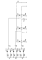
図1の構成図において、充電装置100は、n個のバッテリセル(蓄電器セル)E1,E2,…,Enが直列接続されたバッテリ(バッテリ)20と、各バッテリセルE1,E2,…,Enを充電する充電回路10と、充電回路10を駆動する矩形波を生成する周期電源(矩形波電源)であるパルス印加回路30と、各バッテリセルE1,E2,…,Enの電圧を測定するセル電圧検出回路25とを備えている。なお、バッテリ20は負荷に接続されている。また、パルス印加回路は、絶縁回路を経由して車体に接地された車両制御装置と接続される。バッテリ20と充電回路10とパルス印加回路30との基準電位は車体に接地されず絶縁されている。
(First embodiment)
A charging apparatus according to an embodiment of the present invention will be described with reference to the drawings.
In the configuration diagram of FIG. 1, the charging device 100 includes a battery (battery) 20 in which n battery cells (capacitor cells) E1, E2,..., En are connected in series, and each battery cell E1, E2,. A charging circuit 10 for charging the battery, a pulse applying circuit 30 which is a periodic power source (rectangular wave power source) for generating a rectangular wave for driving the charging circuit 10, and a cell for measuring the voltage of each of the battery cells E1, E2,. And a voltage detection circuit 25. The battery 20 is connected to a load. The pulse applying circuit is connected to a vehicle control device that is grounded to the vehicle body via an insulating circuit. The reference potentials of the battery 20, the charging circuit 10, and the pulse applying circuit 30 are insulated from the vehicle body without being grounded.
バッテリ20は、代表的にはリチウムイオン電池であり、両端の電位がV0とVnとに維持され、各バッテリセルE1,E2,…,Enの接続点の電位がV1,V2,…,Vn−1に維持されている。言い換えれば、負荷及びバッテリセルE1,E2,…,Enの接続点の電位は、V0,V1,V2,…,Vn−1,Vnである。セル電圧検出回路25は、各バッテリセルE1,E2,…,Enの電位差を検出するようにn個の検出回路から構成されている。各検出回路は、オペアンプ回路OA1,OA2,…,OAnと、各オペアンプ回路OA1,OA2,…,OAnの入力に並列接続されたコンデンサC01,C02,…,C0nと、各コンデンサC01,C02,…,C0nの両端と各バッテリセルE1,E2,…,Enの各接続点との間に接続された抵抗器r11,r12,r21,r22,…,rn1,rn2とを備えている。このコンデンサC01,C02,…,C0nと抵抗器r11,r12,r21,r22,…,rn1,rn2とでノーマルモードノイズを防止している。なお、この各検出回路は、バッテリセルE1,E2,…,Enの充電量を平準化するために必要になったものであり、平準化を行う必要がない充電装置では不要である。また、オペアンプ回路OA1,OA2,…,OAnは、アイソレーションアンプを用いることが好ましい。 The battery 20 is typically a lithium ion battery, the potentials at both ends are maintained at V0 and Vn, and the potentials at the connection points of the battery cells E1, E2,..., En are V1, V2,. 1 is maintained. In other words, the potentials at the connection points of the load and the battery cells E1, E2,..., En are V0, V1, V2,. The cell voltage detection circuit 25 is composed of n detection circuits so as to detect a potential difference between the battery cells E1, E2,. Each detection circuit includes an operational amplifier circuit OA1, OA2, ..., and OAn, the operational amplifier OA1, OA2, ..., capacitor C 01, C 02 connected in parallel to the input of OAn, ..., and C 0n, the capacitors C 01 , C 02 ,..., C 0n and resistors r11, r12, r21, r22,... Rn1, rn2 connected between the battery cells E1, E2,. ing. These capacitor C 01 , C 02 ,..., C 0n and resistors r11, r12, r21, r22,..., Rn1, rn2 prevent normal mode noise. Each detection circuit is required for leveling the charge amounts of the battery cells E1, E2,..., En, and is not necessary for a charging device that does not need to perform leveling. The operational amplifier circuits OA1, OA2,..., OAn preferably use isolation amplifiers.
次に、本実施形態の特徴構成である充電回路10の構成について説明するが、各バッテリセルE1,E2,…,Enについて同一の回路が形成されているので、バッテリセルE1の回路について説明する。バッテリセルE1の陽極には電流制限用の抵抗器R11を介してダイオードD11のカソードが接続され、バッテリセルE1の陰極には抵抗器R12を介してダイオードD12のアノードが接続されている。ダイオードD11のアノードとダイオードD12のカソードとはコンデンサC1の一端に接続され、コンデンサC1の他端にはパルス印加回路30の出力信号が入力されている。なお、バッテリセルEnの陰極を充電装置の基準電位とする。 Next, the configuration of the charging circuit 10 that is a characteristic configuration of the present embodiment will be described. Since the same circuit is formed for each of the battery cells E1, E2,..., En, the circuit of the battery cell E1 will be described. . The cathode of the diode D11 is connected to the anode of the battery cell E1 via a resistor R11 for current limitation, and the anode of the diode D12 is connected to the cathode of the battery cell E1 via a resistor R12. The anode of the diode D11 and the cathode of the diode D12 are connected to one end of the capacitor C1, and the output signal of the pulse applying circuit 30 is input to the other end of the capacitor C1. The cathode of the battery cell En is used as the reference potential of the charging device.
パルス印加回路30は、充電回路10の各コンデンサC1,C2,…,Cnの他端にパルス電圧を印加する回路が複数設けられている。ここでは、説明の都合上、コンデンサC1の他端に接続される回路について説明する。パルス印加回路30は、Hi側のスイッチS1とLo側のスイッチS2との直列回路が基準電位との間で電源電位Vpに維持されており、スイッチS1とスイッチS2との接続点がコンデンサC1の他端に接続されている。スイッチS1は制御回路によるパルス電圧により制御され、スイッチS2はこのパルス電圧をインバータINVにより反転した反転信号により制御される。これにより、スイッチS1がOFF状態からON状態に遷移し、スイッチS2がON状態からOFF状態に遷移するときには、コンデンサC1の他端が基準電位から電源電位Vpに遷移する。一方、スイッチS1がON状態からOFF状態に遷移し、スイッチS2がOFF状態からONに遷移するときには、コンデンサC1の他端が電源電位Vpから基準電位に遷移する。 The pulse application circuit 30 is provided with a plurality of circuits for applying a pulse voltage to the other ends of the capacitors C1, C2,. Here, for convenience of explanation, a circuit connected to the other end of the capacitor C1 will be described. In the pulse application circuit 30, the series circuit of the Hi-side switch S1 and the Lo-side switch S2 is maintained at the power supply potential Vp between the reference potential and the connection point between the switch S1 and the switch S2 is the capacitor C1. Connected to the other end. The switch S1 is controlled by a pulse voltage by the control circuit, and the switch S2 is controlled by an inverted signal obtained by inverting this pulse voltage by the inverter INV. As a result, when the switch S1 changes from the OFF state to the ON state and the switch S2 changes from the ON state to the OFF state, the other end of the capacitor C1 changes from the reference potential to the power supply potential Vp. On the other hand, when the switch S1 transitions from the ON state to the OFF state and the switch S2 transitions from the OFF state to ON, the other end of the capacitor C1 transitions from the power supply potential Vp to the reference potential.
次に、図2を参照して充電装置100の動作を説明する。
図2(a)は基準電位から電源電位Vpに遷移し、コンデンサからセル充電するときの動作を説明するための図であり、図2(b)は電源電位Vpから基準電位に遷移し、コンデンサ再充電するときの動作を説明するための図である。
図2(a)において、コンデンサC1の他端が基準電位から電源電位Vp(図1)に遷移すると、コンデンサC1の電位が全体的に電源電位Vpだけ上昇するため、コンデンサC1、ダイオードD11、及び抵抗器R11を介してバッテリセルE1,E2,…,Enに電流i+が流れる。一方、バッテリセルE1の陰極電位V1は全体的に電源電位Vpだけ上昇したコンデンサC1の電位よりも低くなるので、ダイオードD12はOFF状態となる。これにより、C1の電荷が放電されダイオードに接続された側のコンデンサ端子の電位はV0の電位に収束する。なお、矩形波電圧の瞬時電圧である電源電位Vpは基準電位よりも高い。
Next, the operation of the charging apparatus 100 will be described with reference to FIG.
FIG. 2A is a diagram for explaining the operation when the cell is charged from the capacitor by transitioning from the reference potential to the power supply potential Vp, and FIG. 2B is the diagram illustrating the transition from the power supply potential Vp to the reference potential. It is a figure for demonstrating operation | movement when recharging.
In FIG. 2A, when the other end of the capacitor C1 transitions from the reference potential to the power supply potential Vp (FIG. 1), the potential of the capacitor C1 rises as a whole by the power supply potential Vp, so that the capacitor C1, the diode D11, and A current i + flows to the battery cells E1, E2, ..., En via the resistor R11. On the other hand, the cathode potential V1 of the battery cell E1 is generally lower than the potential of the capacitor C1 which is increased by the power supply potential Vp, so that the diode D12 is turned off. Thereby, the electric charge of C1 is discharged, and the electric potential of the capacitor terminal on the side connected to the diode converges to the electric potential of V0. Note that the power supply potential Vp, which is an instantaneous voltage of a rectangular wave voltage, is higher than the reference potential.
また、図2(b)において、コンデンサC1の他端が電源電位Vpから基準電位に遷移すると、コンデンサC1の電位が全体的に電源電位Vpだけ低下するため、抵抗器R12、ダイオードD12、及びコンデンサC1を介してバッテリセルE2,…,Enから電流i−が放電する。一方、バッテリセルE1の陽極電位V0は全体的に電源電位Vpだけ低下したコンデンサC1の電位よりも高くなるので、ダイオードD11はOFF状態となる。これにより、C1に電荷が充電されダイオードに接続された側のコンデンサ端子の電位はV1の電位に収束する。 Further, in FIG. 2B, when the other end of the capacitor C1 transitions from the power supply potential Vp to the reference potential, the potential of the capacitor C1 is lowered by the power supply potential Vp as a whole, so that the resistor R12, the diode D12, and the capacitor The current i − is discharged from the battery cells E2,..., En via C1. On the other hand, the anode potential V0 of the battery cell E1 becomes higher than the potential of the capacitor C1 that is lowered by the power supply potential Vp as a whole, so that the diode D11 is turned off. As a result, the potential of the capacitor terminal on the side where the charge is charged in C1 and connected to the diode converges to the potential of V1.
図2(a)の状態でバッテリセルE1,E2,…,Enが充電される一方、図2(b)の状態でバッテリセルE2,…,Enの電荷が放電されるので、結果的に、バッテリセルE1のみが充電される。 In the state of FIG. 2A, the battery cells E1, E2,..., En are charged, while in the state of FIG. 2B, the battery cells E2,. Only the battery cell E1 is charged.
図3は、n=3の場合であって、中段のバッテリセルE2にのみ充電を行う場合の回路動作結果を示す。
パルス印加回路30(図1)は、図3において、pチャネルMOSFET M11,M21,M31とnチャネルMOSFET M12,M22,M32との接続回路で構成され、pチャネルMOSFET M21とnチャネルMOSFET M22とのゲートにパルス信号Vsが入力される。なお、MOSFETM11,M12,M31,M32のゲートは基準電位に維持されている。
FIG. 3 shows a circuit operation result in the case where n = 3 and only the middle-stage battery cell E2 is charged.
The pulse application circuit 30 (FIG. 1) is composed of a connection circuit of p-channel MOSFETs M11, M21, and M31 and n-channel MOSFETs M12, M22, and M32 in FIG. 3, and includes a p-channel MOSFET M21 and an n-channel MOSFET M22. A pulse signal Vs is input to the gate. Note that the gates of the MOSFETs M11, M12, M31, and M32 are maintained at the reference potential.
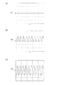
図4(a)はバッテリセルE1に流れる電流波形であり、図4(b)はバッテリセルE2に流れる電流波形であり、図4(c)はバッテリセルE3に流れる電流波形である。図3の回路においては、図4(a)に示すように、バッテリセルE1は充放電がされず、図4(b)に示すように、バッテリセルE2にはダイオードD21を介した充電電流のみが流れ、放電電流が流れない。また、図4(c)に示すように、バッテリセルE3には、ダイオードD21を介した充電電流とダイオードD22を介した放電電流とが交互に流れ、充電電流と放電電流とがバランスした定常状態では、平均電流がゼロとなる。 4A shows the current waveform flowing through the battery cell E1, FIG. 4B shows the current waveform flowing through the battery cell E2, and FIG. 4C shows the current waveform flowing through the battery cell E3. In the circuit of FIG. 3, as shown in FIG. 4A, the battery cell E1 is not charged / discharged, and as shown in FIG. 4B, the battery cell E2 only has a charging current via the diode D21. Flows and no discharge current flows. Further, as shown in FIG. 4C, the battery cell E3 is alternately supplied with the charging current via the diode D21 and the discharging current via the diode D22, and the steady state in which the charging current and the discharging current are balanced. Then, the average current becomes zero.
以上説明したように、本実施形態によれば、バッテリセルE1,E2,…,En及び負荷の接続点とパルス印加回路30とがコンデンサC1,C2,…,Cnを介して絶縁され、このコンデンサに各極の電位とパルス印加回路30との電位差に相当する電圧が充電される。また、パルス印加回路30が生成する矩形波電圧の電圧が電源電圧Vpに維持されているときにバッテリセルE1の陽極を介して、この陽極と基準電位との間で接続された複数のバッテリセルE1,E2,E3,…,Enに充電される。また、矩形波電源の電圧が基準電位に対する電圧であるときにバッテリセルE1とバッテリセルE2との接続点を介して、この接続点と基準電位との間で接続された単数あるいは複数のバッテリセルE2,E3,…,Enから電荷が放電される。この充電及び放電により、バッテリセルE1にのみ充電される。また、バッテリ20とパルス印加回路30とは共通電位で接続されているので、コモンモードノイズがコンデンサC1,C2,…,Cnに充電されにくい。 As described above, according to the present embodiment, the connection points of the battery cells E1, E2,..., En and the load and the pulse application circuit 30 are insulated via the capacitors C1, C2,. In addition, a voltage corresponding to the potential difference between each electrode and the pulse application circuit 30 is charged. A plurality of battery cells connected between the anode and the reference potential via the anode of the battery cell E1 when the voltage of the rectangular wave voltage generated by the pulse applying circuit 30 is maintained at the power supply voltage Vp. E1, E2, E3,..., En are charged. In addition, when the voltage of the rectangular wave power supply is a voltage with respect to the reference potential, the battery cell or cells connected between the connection point and the reference potential via the connection point between the battery cell E1 and the battery cell E2 Charges are discharged from E2, E3,. By this charging and discharging, only the battery cell E1 is charged. Further, since the battery 20 and the pulse applying circuit 30 are connected at a common potential, common mode noise is unlikely to be charged in the capacitors C1, C2,.
(第2実施形態)
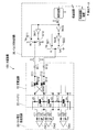
前記第1実施形態は、一のバッテリセルE1の充電を行うために、他のバッテリセルE2,E3,…,Enの充放電を行ったが、バッテリセルE1のみに充電を行うことができる。本実施形態の充電装置を図5の構成図を用いて説明する。
充電装置150は、セル電圧検出回路25と、バッテリ20と、充電回路15と、パルス印加回路35とを備える。セル電圧検出回路25とバッテリ20とは第1実施形態と同様の構成であるので説明を省略し、充電回路15と、パルス印加回路35とについて説明する。なお、第1実施形態と同様にバッテリセルEnの陰極を基準電位としてパルス印加回路35が接続されている。
(Second Embodiment)
In the first embodiment, in order to charge one battery cell E1, the other battery cells E2, E3,..., En are charged / discharged, but only the battery cell E1 can be charged. The charging apparatus of this embodiment is demonstrated using the block diagram of FIG.
The charging device 150 includes a cell voltage detection circuit 25, a battery 20, a charging circuit 15, and a pulse application circuit 35. Since the cell voltage detection circuit 25 and the battery 20 have the same configuration as that of the first embodiment, the description thereof will be omitted, and the charging circuit 15 and the pulse application circuit 35 will be described. As in the first embodiment, the pulse application circuit 35 is connected with the cathode of the battery cell En as a reference potential.
充電回路15は、各バッテリセルE1,E2,…,En毎に充電を行うものであり、同一の複数の回路によって構成されている。たとえば、バッテリセルE1を充電する回路は、ダイオードD11,D12,D13,D14とコンデンサC11,C12と抵抗器R11,R12とを備える。バッテリ20を構成するバッテリセルE1の陽極には、ダイオードD11のカソードとダイオードD13のカソードとが接続され、バッテリセルE1の陰極には、ダイオードD12のアノードとダイオードD14のアノードとが接続される。また、ダイオードD11のアノードとダイオードD12のアノードとはコンデンサC11と抵抗器R11とを介してパルス信号が入力される。また、ダイオードD13のカソードとダイオードD14のカソードとにはコンデンサC14と抵抗器R12とを介してパルス信号を反転した反転信号が入力される。なお、ダイオードD11,D12,D13,D14は全波整流回路を構成している。 The charging circuit 15 performs charging for each of the battery cells E1, E2,..., En, and includes a plurality of identical circuits. For example, the circuit for charging the battery cell E1 includes diodes D11, D12, D13, and D14, capacitors C11 and C12, and resistors R11 and R12. The anode of the battery cell E1 constituting the battery 20 is connected to the cathode of the diode D11 and the cathode of the diode D13, and the cathode of the battery cell E1 is connected to the anode of the diode D12 and the anode of the diode D14. A pulse signal is input to the anode of the diode D11 and the anode of the diode D12 via the capacitor C11 and the resistor R11. Further, an inverted signal obtained by inverting the pulse signal is input to the cathode of the diode D13 and the cathode of the diode D14 via the capacitor C14 and the resistor R12. The diodes D11, D12, D13, and D14 constitute a full wave rectifier circuit.
パルス印加回路35は、充電回路15の抵抗器R11に印加するパルス信号と、このパルス信号の反転信号を生成する。Hi側のスイッチS11とLo側のスイッチS12との直列回路が基準電位との間で電源電位Vpに維持されており、スイッチS21とスイッチS22との接続点が抵抗器R12に接続されている。また、Hi側のスイッチS21とLo側のスイッチS22との直列回路が基準電位との間で電源電位Vpに維持されており、スイッチS21とスイッチS22との接続点が抵抗器R12に接続されている。 The pulse application circuit 35 generates a pulse signal to be applied to the resistor R11 of the charging circuit 15 and an inverted signal of this pulse signal. A series circuit of the Hi-side switch S11 and the Lo-side switch S12 is maintained at the power supply potential Vp between the reference potential and the connection point between the switch S21 and the switch S22 is connected to the resistor R12. In addition, the series circuit of the Hi-side switch S21 and the Lo-side switch S22 is maintained at the power supply potential Vp between the reference potential and the connection point between the switch S21 and the switch S22 is connected to the resistor R12. Yes.
スイッチS11は制御回路によるパルス信号により制御され、スイッチS12はこのパルス電圧をインバータINV1により反転した反転信号により制御される。また、スイッチS21は制御回路によるパルス信号をインバータINV3で反転した信号により制御され、スイッチS22はインバータINV3で反転した信号をインバータINV2で反転した信号で制御される。これにより、スイッチS11とスイッチS12との接続点の電位は、スイッチS21とスイッチS22との接続点の電位に対して反転する。 The switch S11 is controlled by a pulse signal from the control circuit, and the switch S12 is controlled by an inverted signal obtained by inverting this pulse voltage by the inverter INV1. The switch S21 is controlled by a signal obtained by inverting the pulse signal from the control circuit by the inverter INV3, and the switch S22 is controlled by a signal obtained by inverting the signal inverted by the inverter INV3 by the inverter INV2. As a result, the potential at the connection point between the switch S11 and the switch S12 is inverted with respect to the potential at the connection point between the switch S21 and the switch S22.
次に、図6を参照して、充電装置150の動作について説明する。
図6(a)は抵抗器R11に正のパルス信号を印加し、抵抗器R12に反転信号を印加した場合を示し、図6(b)は抵抗器R12に正のパルス信号を印加し、抵抗器R11に反転信号を印加した場合を示している。
図6(a)においては、抵抗器R11、コンデンサC11、ダイオードD11、バッテリセルE1、ダイオードD14、コンデンサC12、抵抗器R12の経路で電流が流れ、バッテリセルE1が充電される。なお、この状態では、ダイオードD12,D13はOFF状態にされている。また、図6(b)においては、抵抗器R12、コンデンサC12、ダイオードD13、バッテリセルE1、ダイオードD12、コンデンサC11、及び、抵抗器R11の経路で電流が流れ、バッテリセルE1が充電される。なお、この状態では、ダイオードD11,D14はOFF状態にされている。
Next, the operation of the charging device 150 will be described with reference to FIG.
FIG. 6A shows a case where a positive pulse signal is applied to the resistor R11 and an inverted signal is applied to the resistor R12. FIG. 6B shows a case where a positive pulse signal is applied to the resistor R12, The case where an inversion signal is applied to the device R11 is shown.
In FIG. 6A, current flows through the path of the resistor R11, the capacitor C11, the diode D11, the battery cell E1, the diode D14, the capacitor C12, and the resistor R12, and the battery cell E1 is charged. In this state, the diodes D12 and D13 are turned off. In FIG. 6B, a current flows through the path of the resistor R12, the capacitor C12, the diode D13, the battery cell E1, the diode D12, the capacitor C11, and the resistor R11, and the battery cell E1 is charged. In this state, the diodes D11 and D14 are turned off.
次に、本実施形態の回路動作結果について説明する。
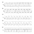
図7は、n=2の場合であって、バッテリセルE1にのみ充電を行う場合の回路図であり、図8は各部の電圧および電流波形である。
このとき、ダイオードD11に流れる電流が電流IAであり、ダイオードD13に流れる電流が電流IBであり、バッテリセルE1に流れる電流が電流Icである。
Next, the circuit operation result of this embodiment will be described.
FIG. 7 is a circuit diagram in the case where n = 2 and only the battery cell E1 is charged, and FIG. 8 is a voltage and current waveform of each part.
At this time, the current flowing through the diode D11 is a current I A, the current flowing through the diode D13 is a current I B, the current flowing through the battery cell E1 is a current I c.
図8(a)はパルス信号VAの波形であり、図8(b)は反転信号VBの波形であり、図8(c)は電流IAの波形であり、図8(d)は電流IBの波形であり、図8(e)は電流ICの波形である。これらの波形の横軸は時間Tを示している。パルス信号VAが高位相のときに電流IAが流れ、反転信号VBが高位相のときに電流IBが流れている。また、バッテリセルE1に流れる電流ICは、ダイオードD11に流れる電流がIAとダイオードD13に流れる電流がIBとの重ね合わせであり、連続した充電電流が流れる。 8 (a) is a waveform of the pulse signal V A, FIG. 8 (b) is a waveform of the inverted signal V B, Fig. 8 (c) is a waveform of the current I A, FIG. 8 (d) is a waveform of the current I B, FIG. 8 (e) is a waveform of the current I C. The horizontal axis of these waveforms indicates time T. Pulse signal V A is the current I A flows when the high phase, the inverted signal V B is the current I B flows when the high phase. The current I C flowing through the battery cell E1, the current the current flowing through the diode D11 flows in I A and diode D13 is a superposition of the I B, flowing continuous charging current.
以上説明したように、本実施形態によれば、スイッチS11,S12から構成される矩形波電源とスイッチS21,S22から構成される矩形波電源との位相が反転しているから、何れかの矩形波電源の電位の方が高く、他方の電位の方が低い。たとえば、S11,S12から構成される矩形波電源の方が電位の高い場合には、コンデンサC11は電位が高い方の接続点であるバッテリセルE1の陽極の電位に収束し固定される。また、コンデンサC12は、バッテリセルE1の陰極の電位に収束し固定される。したがって、コンデンサC11、バッテリセルE1、コンデンサC12を介して、矩形波電源と矩形波電源との間で電流が流れる。また、この場合も第1実施形態と同様に、バッテリ20の陰極をパルス印加回路35の基準電位としているので、コモンモードノイズがコンデンサC11、C12に充電されにくい。 As described above, according to the present embodiment, the phase of the rectangular wave power source constituted by the switches S11 and S12 and the rectangular wave power source constituted by the switches S21 and S22 are reversed, so that any rectangular shape is obtained. The potential of the wave power source is higher and the other potential is lower. For example, when the rectangular wave power source composed of S11 and S12 has a higher potential, the capacitor C11 converges and is fixed to the potential of the anode of the battery cell E1, which is the connection point with the higher potential. The capacitor C12 converges and is fixed at the cathode potential of the battery cell E1. Therefore, a current flows between the rectangular wave power source and the rectangular wave power source via the capacitor C11, the battery cell E1, and the capacitor C12. Also in this case, as in the first embodiment, since the cathode of the battery 20 is used as the reference potential of the pulse applying circuit 35, common mode noise is unlikely to be charged in the capacitors C11 and C12.
(比較例)
図9を参照して、比較例について説明する。前記各実施形態では、パルス印加回路30,35を用いて矩形波電圧を印加していたが、本比較例では交流電源を用いて駆動する。
図9(a)の回路図(特許文献6参照)において、本比較例の充電装置は、4つのバッテリセルE1,E2,E3,E4が直列接続され、各バッテリセルE1,E2,E3,E4の陽極にダイオードD11,D21,D31,D41のカソードとコンデンサC11,C21,C31,C41の一端とが接続され、各バッテリセルE1,E2,E3,E4の陰極にダイオードD12,D22,D32,D42のアノードが接続され、ダイオードD12,D22,D32,D42のカソードとダイオードD11,D21,D31,D41のアノードと、コンデンサC12,C22,C32,C42の一端とが接続され、コンデンサC11,C21,C31,C41の他端が抵抗器R11,R21,R31,R41を介して交流電源AC1の一端に接続されている。また、コンデンサC12,C22,C32,C42の他端が、抵抗器R12,R22,R32,R42を介して交流電源の他端に接続されている。なお、交流電源AC1と、バッテリセルE1,E2,E3,E4とは共通電位で接続されておらず、コンデンサC11,C21,C31,C41,C12,C22,C32,C42によって絶縁されているのみであるので、コモンモードノイズvnの影響を受ける。
(Comparative example)
A comparative example will be described with reference to FIG. In each of the above embodiments, the rectangular wave voltage is applied using the pulse applying circuits 30 and 35. However, in this comparative example, driving is performed using an AC power supply.
In the circuit diagram of FIG. 9A (see Patent Document 6), in the charging device of this comparative example, four battery cells E1, E2, E3, E4 are connected in series, and each battery cell E1, E2, E3, E4 is connected. The cathodes of the diodes D11, D21, D31, D41 and one ends of the capacitors C11, C21, C31, C41 are connected to the anodes of the diodes D12, D22, D32, D42. Are connected, the cathodes of the diodes D12, D22, D32, D42, the anodes of the diodes D11, D21, D31, D41, and one end of the capacitors C12, C22, C32, C42 are connected, and the capacitors C11, C21, C31 are connected. , C41 is connected to one end of the AC power supply AC1 through resistors R11, R21, R31, R41. It has been continued. The other ends of the capacitors C12, C22, C32, and C42 are connected to the other end of the AC power supply via resistors R12, R22, R32, and R42. The AC power supply AC1 and the battery cells E1, E2, E3, and E4 are not connected at a common potential, and are only insulated by capacitors C11, C21, C31, C41, C12, C22, C32, and C42. Therefore, it is affected by the common mode noise vn.
図9(b)(c)のように、バッテリセルE4の陰極と交流電源AC1の一方とを接続してコモンモードノイズvn(図9(a))の影響を回避しようとすることが考えられる。しかしながら、図9(b)のように抵抗器R12とバッテリセルE4の陰極を共通電位として接続した場合、抵抗器R11、コンデンサC11、バッテリセルE1,E2,E3,E4を介して交流電流が流れるだけであり、充電が行われない。また、図9(c)のように抵抗器R11とバッテリセルE4の陰極を共通電位として接続した場合は、ダイオードD11,D21,D31,D41とダイオードD12,D22,D32,D34との接続点に交流電圧が印加されるようにした回路であるが、コンデンサC12,C22,C32,C42を介して交流電流が流れ、コンデンサC11,C21,C31,C41にはいずれの方向の電流も流れない。このため、図9(c)の回路は、実質的に第1実施形態(図1)と同様の回路構成である。 As shown in FIGS. 9B and 9C, it is conceivable to connect the cathode of the battery cell E4 and one of the AC power supplies AC1 to avoid the influence of the common mode noise vn (FIG. 9A). . However, when the resistor R12 and the cathode of the battery cell E4 are connected as a common potential as shown in FIG. 9B, an alternating current flows through the resistor R11, the capacitor C11, and the battery cells E1, E2, E3, and E4. Only and no charging is done. When the resistor R11 and the cathode of the battery cell E4 are connected as a common potential as shown in FIG. 9C, the connection point between the diodes D11, D21, D31, D41 and the diodes D12, D22, D32, D34 is used. In this circuit, an alternating voltage is applied, but an alternating current flows through the capacitors C12, C22, C32, and C42, and no current in any direction flows through the capacitors C11, C21, C31, and C41. For this reason, the circuit of FIG. 9C has a circuit configuration substantially similar to that of the first embodiment (FIG. 1).
次に、図10を参照して図9(a)の回路を他の視点から検討する。図10(a)(b)は、基準電位に接続された2つの交流電源AC1,AC2を設け、図9(b)(c)と同様に、コモンモードノイズvnの影響を回避するためにバッテリセルE4の陰極を基準電位としている。なお、バッテリセルE1に関連する回路のみを示し、他のバッテリセルE2,E3,E4に関連する回路は省略している。 Next, referring to FIG. 10, the circuit of FIG. 9A will be examined from another viewpoint. FIGS. 10A and 10B are provided with two AC power supplies AC1 and AC2 connected to a reference potential, and in the same manner as FIGS. 9B and 9C, a battery for avoiding the influence of common mode noise vn. The cathode of the cell E4 is set as a reference potential. Only circuits related to the battery cell E1 are shown, and circuits related to the other battery cells E2, E3, and E4 are omitted.
図10(a)において、交流電源AC1については、抵抗器R11及びコンデンサC11を介してバッテリセルE1,E2,E3,E4に交流電流が流れるのみであり、バッテリセルE1への充電が行われない。交流電源AC2については、正の電圧のとき抵抗器R12、コンデンサC12、ダイオードD11を介してバッテリセルE1,E2,E3,E4に正方向の電流が流れる。また、負の電圧のとき、ダイオードD12、コンデンサC12、抵抗器R12を介して負方向の電流が流れ、バッテリセルE2,E3,E4を放電させる。したがって、バッテリセルE1のみが充電され、バッテリセルE2,E3,E4は充電されない。 In FIG. 10A, with respect to the AC power supply AC1, only an AC current flows through the battery cells E1, E2, E3, and E4 via the resistor R11 and the capacitor C11, and the battery cell E1 is not charged. . For AC power supply AC2, a positive current flows through battery cells E1, E2, E3, and E4 via resistor R12, capacitor C12, and diode D11 when the voltage is positive. When the voltage is negative, a negative current flows through the diode D12, the capacitor C12, and the resistor R12 to discharge the battery cells E2, E3, and E4. Therefore, only the battery cell E1 is charged, and the battery cells E2, E3, E4 are not charged.
図10(b)においては、コンデンサC11及びダイオードD11とバッテリセルE1の陽極との間にダイオードD13が挿入されている。交流電源AC1と交流電源AC2との位相差が180度であって、交流電源AC1が正の電位であり、交流電源AC2が負の電位である場合には、抵抗器R11、コンデンサC11、ダイオードD13、バッテリセルE1、ダイオードD12、コンデンサC12、抵抗器R12の経路で電流が流れる。一方、交流電源AC1が負の電位であり、交流電源AC2が正の電位である場合には、抵抗器R12、コンデンサC12、ダイオードD11、コンデンサC11、抵抗器R11の経路で電流が流れる。したがって、バッテリセルE1のみ充電され、バッテリセルE2,E3,E4は充電されない。 In FIG. 10B, the diode D13 is inserted between the capacitor C11 and the diode D11 and the anode of the battery cell E1. When the phase difference between the AC power source AC1 and the AC power source AC2 is 180 degrees, the AC power source AC1 is a positive potential, and the AC power source AC2 is a negative potential, the resistor R11, the capacitor C11, and the diode D13. A current flows through the path of the battery cell E1, the diode D12, the capacitor C12, and the resistor R12. On the other hand, when the AC power supply AC1 has a negative potential and the AC power supply AC2 has a positive potential, a current flows through the path of the resistor R12, the capacitor C12, the diode D11, the capacitor C11, and the resistor R11. Therefore, only the battery cell E1 is charged, and the battery cells E2, E3, E4 are not charged.
図10(c)の充電装置は、図10(b)のダイオードD13を抵抗器R1に置き換え、D12をR3に置き換えたものである。交流電源AC1が正の電位であり、交流電源AC2が負の電位であるとき、抵抗器R11、コンデンサC1、抵抗器R1、バッテリセルE1、抵抗器R3、コンデンサC2、抵抗器R12の経路でバッテリセルE1に充電電流が流れる。これに対して、交流電源AC1が負の電位であり、交流電源AC2が正の電位であるときは、2つの電流経路が存在する。第1の経路は、抵抗器R12、コンデンサC2、ダイオードD11、コンデンサC1、抵抗器R11の経路であり、第2の経路は、抵抗器R12、コンデンサC2、抵抗器R3、バッテリセルE1、抵抗器R1、コンデンサC1、抵抗器R11の経路である。 The charging device in FIG. 10C is obtained by replacing the diode D13 in FIG. 10B with a resistor R1 and replacing D12 with R3. When the AC power supply AC1 is at a positive potential and the AC power supply AC2 is at a negative potential, the battery passes through the path of the resistor R11, the capacitor C1, the resistor R1, the battery cell E1, the resistor R3, the capacitor C2, and the resistor R12. A charging current flows through the cell E1. On the other hand, when the AC power supply AC1 has a negative potential and the AC power supply AC2 has a positive potential, there are two current paths. The first path is the path of the resistor R12, the capacitor C2, the diode D11, the capacitor C1, and the resistor R11, and the second path is the resistor R12, the capacitor C2, the resistor R3, the battery cell E1, and the resistor. This is the path of R1, capacitor C1, and resistor R11.
この場合は、ダイオードの本数が少ない利点がある一方、第2の経路はバッテリセルE1に充電された電荷を放電させることになる。なお、交流電源AC1と交流電源AC2との振幅が等しく、コンデンサC1とコンデンサC2との容量が等しく、抵抗器R1と抵抗器R3との抵抗値が等しく、抵抗器R11と抵抗器R12との抵抗値が等しければ、バッテリセルE2,E3,E4は充電されない。 In this case, there is an advantage that the number of diodes is small, while the second path discharges the electric charge charged in the battery cell E1. The AC power supply AC1 and the AC power supply AC2 have the same amplitude, the capacitors C1 and C2 have the same capacitance, the resistors R1 and R3 have the same resistance value, and the resistors R11 and R12 have the same resistance. If the values are equal, the battery cells E2, E3, E4 are not charged.
(変形例)
本発明は前記した実施形態に限定されるものではなく、例えば以下のような種々の変形が可能である。
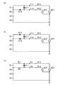
(1)前記第2実施形態は、バッテリセルEnの陰極をパルス印加回路35のスイッチS12,S22の基準電位としていたが他のバッテリセルE1,E2,…,En−1を基準電位とすることもできる。具体的には、図11(a)は、最大電位であるバッテリセルE0の陽極を基準電位としたものであり、図11(b)は、中間電位であるバッテリセルE2の陰極すなわちバッテリセルE3の陽極を基準電位としたものである。
(2)前記第2実施形態は、バッテリセルE1,E2,…,Enに直接ダイオードD11,D12,D13,D14を接続していたため、図8(e)に示したようにバッテリセルE1に流れる電流ICはパルス状のノイズ成分を含んでいる。図12に示すように、バッテリセルE1の両端に抵抗器r1,r2の一端を接続し、抵抗器r1,r2の他端にコンデンサC0を接続して、ノイズ成分を除去することができる。
(3)前記各実施形態は、パルス印加回路30,35が生成した矩形波を用いて充電回路10を駆動したが、正弦波を用いて充電回路10を駆動することができる。
(4)前記各実施形態は、通電経路の途中に電流量を制限するための抵抗器を挿入しているが、抵抗器の代わりにインダクタを挿入しても同様の効果が得られる。また、抵抗器とインダクタを直列に接続して挿入することで、より低抵抗の抵抗器でも電流量を制限できるため、抵抗で消費される電力を小さくすることができる。電流量を制限するための抵抗器あるいはインダクタは通電経路上であれば任意の箇所に配置することができ、複数に分割することもできる。また、インダクタとコンデンサとを含む回路の共振周波数と矩形波電圧の周波数とを近似させると、バッテリセルE1,E2,…,Enに充電される電圧がパルス印加回路30,35が生成する矩形波電圧よりも高くなることがある。この場合には、パルス印加回路30,35が生成する矩形波電圧は、バッテリセルE1,E2,…,Enの電圧よりも低くても構わない。
(5)前記各実施形態は、蓄電器としてバッテリ20を用いたが、キャパシタにも適用可能である。
(Modification)
The present invention is not limited to the embodiments described above, and various modifications such as the following are possible.
(1) In the second embodiment, the cathode of the battery cell En is used as the reference potential of the switches S12 and S22 of the pulse application circuit 35. However, the other battery cells E1, E2,. You can also. Specifically, FIG. 11A shows the maximum potential of the anode of the battery cell E0 as the reference potential, and FIG. 11B shows the cathode of the battery cell E2 that is the intermediate potential, that is, the battery cell E3. The anode is used as a reference potential.
(2) In the second embodiment, since the diodes D11, D12, D13, and D14 are directly connected to the battery cells E1, E2,..., En, the battery cell E1 flows as shown in FIG. current I C includes a pulse-like noise component. As shown in FIG. 12, it is possible to remove noise components by connecting one end of resistors r1 and r2 to both ends of the battery cell E1 and connecting a capacitor C0 to the other end of the resistors r1 and r2.
(3) In each of the above embodiments, the charging circuit 10 is driven using the rectangular wave generated by the pulse applying circuits 30 and 35. However, the charging circuit 10 can be driven using a sine wave.
(4) In each of the above embodiments, a resistor for limiting the amount of current is inserted in the middle of the energization path, but the same effect can be obtained by inserting an inductor instead of the resistor. In addition, by connecting the resistor and the inductor in series, the amount of current can be limited even by a resistor having a lower resistance, so that the power consumed by the resistor can be reduced. Resistors or inductors for limiting the amount of current can be arranged at any location on the energization path, and can be divided into a plurality. Further, when the resonance frequency of the circuit including the inductor and the capacitor is approximated with the frequency of the rectangular wave voltage, the rectangular wave generated by the pulse applying circuits 30 and 35 is generated by the voltages charged in the battery cells E1, E2,. May be higher than voltage. In this case, the rectangular wave voltages generated by the pulse applying circuits 30 and 35 may be lower than the voltages of the battery cells E1, E2,.
(5) In each of the above embodiments, the battery 20 is used as a capacitor, but it can also be applied to a capacitor.
10,15 充電回路
20 バッテリ(蓄電器)
25 セル電圧検出回路
30,35 パルス印加回路
100,150 充電装置
E1,E2,E3,E4,En バッテリセル(蓄電器セル)
D11,D12,D13,D14,D21,D22 ダイオード
C0,C1,C2,C11,C12 コンデンサ
S1,S2,S11,S12,S21,S22 スイッチ
AC1,AC2 交流電源
10, 15 Charging circuit 20 Battery (capacitor)
25 Cell voltage detection circuit 30, 35 Pulse application circuit 100, 150 Charging device
E1, E2, E3, E4, En Battery cell (capacitor cell)
D11, D12, D13, D14, D21, D22 Diode C0, C1, C2, C11, C12 Capacitor S1, S2, S11, S12, S21, S22 Switch AC1, AC2 AC power supply
Claims (5)
前記第1周期電源は、前記複数のコンデンサの中から特定した特定コンデンサの他端と前記基準電位点との間に接続され、
前記第2周期電源は、前記特定コンデンサに隣接する隣接コンデンサの他端と前記基準電位点との間に接続され、
前記整流手段は、前記特定コンデンサの一端と前記蓄電器セルの一方の極との間に接続された第1整流手段と、前記隣接コンデンサの一端と前記蓄電器セルの他方の極との間に接続された第2整流手段と、前記特定コンデンサの一端と前記隣接コンデンサの一端との間に接続される第3整流手段とを備え、
前記第1整流手段と前記第2整流手段と前記第3整流手段との直列回路は、同一整流方向に接続されていることを特徴とする充電装置。 A plurality of capacitor cells are connected in series, a capacitor having a pole of any one of the capacitor cells as a reference potential point, one pole of each of the capacitor cells, and the other pole of any of the plurality of capacitor cells Is connected between one or a plurality of capacitors whose potential at one end is fixed via a rectifying means and any other end of the plurality of capacitors and the reference potential point of the capacitor to generate a repetitive signal. A first periodic power supply, and a second periodic power supply that generates an inverted signal of the repetitive signal,
The first periodic power supply is connected between the other end of the specific capacitor identified from the plurality of capacitors and the reference potential point,
The second periodic power supply is connected between the other end of the adjacent capacitor adjacent to the specific capacitor and the reference potential point;
The rectifying means is connected between a first rectifying means connected between one end of the specific capacitor and one pole of the capacitor cell, and between one end of the adjacent capacitor and the other pole of the capacitor cell. Second rectifying means, and third rectifying means connected between one end of the specific capacitor and one end of the adjacent capacitor,
It said first series circuit of the rectifier means and said second rectifying means and the third rectifying means, charging device you characterized in that it is connected to the same rectification direction.
何れかの前記蓄電器セルの正極の電位に第1整流手段を介して一端の電位が固定される第1コンデンサと、
何れかの前記蓄電器セルの負極の電位に第2整流手段を介して一端の電位が固定される第2コンデンサと、
前記第1コンデンサの他端と前記蓄電器の基準電位点との間に接続され、繰り返し信号を生成する第1周期電源と、
前記第2コンデンサの他端と前記基準電位点との間に接続され、前記繰り返し信号の反転信号を生成する第2周期電源と、
前記蓄電器セルの正極にカソード端が接続された前記第1整流手段、及び前記蓄電池セルの負極にアノード端が接続された前記第2整流手段と同一整流方向に直列接続された第3整流手段と、
を備えることを特徴とする充電装置。 A plurality of capacitor cells are connected in series, and a capacitor having a reference potential point as a pole of any one of the capacitor cells;
A first capacitor in which the potential of one end is fixed to the potential of the positive electrode of any one of the battery cells via the first rectifier;
A second capacitor in which the potential at one end is fixed to the potential of the negative electrode of any one of the capacitor cells via a second rectifier;
A first periodic power source connected between the other end of the first capacitor and a reference potential point of the capacitor and generating a repetitive signal;
A second periodic power source connected between the other end of the second capacitor and the reference potential point and generating an inverted signal of the repetitive signal;
A first rectifier having a cathode connected to the positive electrode of the battery cell; and a third rectifier connected in series in the same rectifying direction as the second rectifier connected to the anode of the negative electrode of the storage battery cell; ,
A charging device comprising:
前記第2周期電源は、前記矩形波電圧の反転電圧を発生し、
前記矩形波電圧の中心電圧と前記反転電圧の中心電圧とは一定の電位差を有する
ことを特徴とする請求項1又は請求項2に記載の充電装置。 The first periodic power supply generates a rectangular wave voltage;
The second periodic power supply generates an inverted voltage of the rectangular wave voltage,
3. The charging device according to claim 1, wherein a center voltage of the rectangular wave voltage and a center voltage of the inverted voltage have a constant potential difference.
Priority Applications (4)
| Application Number | Priority Date | Filing Date | Title |
|---|---|---|---|
| JP2006272504A JP4359301B2 (en) | 2006-10-04 | 2006-10-04 | Charger |
| DE200710045836 DE102007045836A1 (en) | 2006-10-04 | 2007-09-25 | loader |
| CN2007101624233A CN101159384B (en) | 2006-10-04 | 2007-09-29 | Charging device |
| US11/905,762 US7936149B2 (en) | 2006-10-04 | 2007-10-03 | Charging device |
Applications Claiming Priority (1)
| Application Number | Priority Date | Filing Date | Title |
|---|---|---|---|
| JP2006272504A JP4359301B2 (en) | 2006-10-04 | 2006-10-04 | Charger |
Publications (3)
| Publication Number | Publication Date |
|---|---|
| JP2008092717A JP2008092717A (en) | 2008-04-17 |
| JP2008092717A5 JP2008092717A5 (en) | 2008-07-24 |
| JP4359301B2 true JP4359301B2 (en) | 2009-11-04 |
Family
ID=39154848
Family Applications (1)
| Application Number | Title | Priority Date | Filing Date |
|---|---|---|---|
| JP2006272504A Expired - Fee Related JP4359301B2 (en) | 2006-10-04 | 2006-10-04 | Charger |
Country Status (4)
| Country | Link |
|---|---|
| US (1) | US7936149B2 (en) |
| JP (1) | JP4359301B2 (en) |
| CN (1) | CN101159384B (en) |
| DE (1) | DE102007045836A1 (en) |
Families Citing this family (22)
| Publication number | Priority date | Publication date | Assignee | Title |
|---|---|---|---|---|
| JP5035895B2 (en) * | 2007-09-27 | 2012-09-26 | 本田技研工業株式会社 | Power generation control device |
| JP5397885B2 (en) * | 2008-10-30 | 2014-01-22 | 独立行政法人 宇宙航空研究開発機構 | Power system |
| JP5564864B2 (en) * | 2008-12-19 | 2014-08-06 | 日産自動車株式会社 | Secondary battery system |
| JP2010193598A (en) * | 2009-02-17 | 2010-09-02 | Nippon Soken Inc | Noncontact power supply facility and noncontact power supply system |
| JP4691171B2 (en) | 2009-03-11 | 2011-06-01 | 本田技研工業株式会社 | Charge / discharge device |
| KR101630489B1 (en) * | 2009-06-30 | 2016-06-14 | 스캔디노바 시스템즈 에이비 | Capacitor charger system and digital control module and isolated acquisition module for such a capacitor charger system |
| EP2302757B1 (en) | 2009-09-24 | 2020-04-29 | VITO NV (Vlaamse Instelling voor Technologisch Onderzoek NV) | Method and system for balancing electrical energy storage cells |
| FR2956260B1 (en) | 2010-02-05 | 2012-04-13 | Commissariat Energie Atomique | CHARGE BALANCING SYSTEM FOR BATTERIES |
| ES2521040T3 (en) * | 2010-02-05 | 2014-11-12 | Commissariat à l'énergie atomique et aux énergies alternatives | Load balancing system for batteries |
| JP5427667B2 (en) * | 2010-03-30 | 2014-02-26 | 本田技研工業株式会社 | Charging device and charging device manufacturing method |
| HUP1000311A2 (en) * | 2010-06-14 | 2012-08-28 | Ferenc Stangl | System and method for charge equalisation and/or charring of electrical energy storing units |
| JP5567956B2 (en) * | 2010-09-16 | 2014-08-06 | 矢崎総業株式会社 | Cell voltage equalization device for multiple assembled batteries |
| WO2012070432A1 (en) * | 2010-11-25 | 2012-05-31 | 本田技研工業株式会社 | Charge control device for electric vehicle |
| US20150069830A1 (en) * | 2011-12-26 | 2015-03-12 | Isuda Recreation & Sports Co., Ltd. | Apparatus for parallel connection and protection of batteries of an electric vehicle |
| WO2014022267A1 (en) * | 2012-07-30 | 2014-02-06 | Primus Power Corporation | Pulse charging of a grid interactive battery system |
| JP2015171280A (en) * | 2014-03-10 | 2015-09-28 | ソニー株式会社 | Voltage equalization device and power storage device |
| BR112017027795B1 (en) * | 2015-06-23 | 2022-10-04 | Nissan Motor Co., Ltd | INVERTER WITH LOADING CAPACITY |
| EP3394951A1 (en) | 2015-12-22 | 2018-10-31 | Vito NV | Connectivity check between cells and wiring control electronics with only one switch |
| JPWO2020136907A1 (en) * | 2018-12-28 | 2021-10-21 | 株式会社東芝 | Storage battery device |
| US11569668B2 (en) * | 2020-07-14 | 2023-01-31 | Igrenenergi, Inc. | System and method for dynamic balancing power in a battery pack |
| WO2023028624A1 (en) * | 2021-09-02 | 2023-03-09 | Just Technology Shpk | Battery charge control system |
| WO2023065082A1 (en) * | 2021-10-18 | 2023-04-27 | 深圳市华思旭科技有限公司 | Circuit structure and control method thereof, and power supply device |
Family Cites Families (13)
| Publication number | Priority date | Publication date | Assignee | Title |
|---|---|---|---|---|
| US5982050A (en) * | 1996-03-14 | 1999-11-09 | Fuji Jukogyo Kabushiki Kaisha | Power supply unit for automotive vehicle |
| JPH1132443A (en) | 1997-07-09 | 1999-02-02 | Sanken Electric Co Ltd | Charging device |
| JP3870577B2 (en) | 1998-09-14 | 2007-01-17 | 株式会社デンソー | Variation determination method for battery pack and battery device |
| JP3982666B2 (en) | 1999-07-21 | 2007-09-26 | 株式会社パワーシステム | Capacitor power supply |
| US6172478B1 (en) * | 2000-02-23 | 2001-01-09 | Telxon Corporation | Power distribution in a portable device |
| JP2001339865A (en) | 2000-05-26 | 2001-12-07 | Hitachi Ltd | Cell voltage equalization apparatus, method therefor, hybrid car and manufacturing method of battery assembly |
| US6642693B2 (en) * | 2000-11-21 | 2003-11-04 | Nagano Japan Radio Co., Ltd. | Voltage equalizing apparatus for battery devices |
| JP3630303B2 (en) | 2000-11-21 | 2005-03-16 | 長野日本無線株式会社 | Voltage equalization device for storage element |
| US6583602B2 (en) * | 2001-05-11 | 2003-06-24 | Denso Corporation | Vehicular power supply apparatus and method of controlling the same |
| JP4605952B2 (en) | 2001-08-29 | 2011-01-05 | 株式会社日立製作所 | Power storage device and control method thereof |
| US6771518B2 (en) * | 2002-08-26 | 2004-08-03 | Potentia Semiconductor, Inc. | DC converters |
| CN2648678Y (en) * | 2003-07-16 | 2004-10-13 | 杨福義 | Series independent detection battery pile charger |
| DE102004031216A1 (en) | 2004-06-28 | 2006-01-19 | Siemens Ag | Apparatus and method for charge equalization in series connected energy storage |
-
2006
- 2006-10-04 JP JP2006272504A patent/JP4359301B2/en not_active Expired - Fee Related
-
2007
- 2007-09-25 DE DE200710045836 patent/DE102007045836A1/en not_active Ceased
- 2007-09-29 CN CN2007101624233A patent/CN101159384B/en not_active Expired - Fee Related
- 2007-10-03 US US11/905,762 patent/US7936149B2/en not_active Expired - Fee Related
Also Published As
| Publication number | Publication date |
|---|---|
| DE102007045836A1 (en) | 2008-04-10 |
| CN101159384A (en) | 2008-04-09 |
| CN101159384B (en) | 2010-11-03 |
| JP2008092717A (en) | 2008-04-17 |
| US7936149B2 (en) | 2011-05-03 |
| US20080084184A1 (en) | 2008-04-10 |
Similar Documents
| Publication | Publication Date | Title |
|---|---|---|
| JP4359301B2 (en) | Charger | |
| US8193761B1 (en) | Hybrid power source | |
| US9487095B2 (en) | Charging and discharging device | |
| US9170292B2 (en) | Insulation detection circuit and method thereof | |
| KR20170011625A (en) | Apparatus for balancing battery stack | |
| JP5187407B2 (en) | Auxiliary battery charger | |
| WO2014103613A1 (en) | Ground fault detecting device | |
| JP5744598B2 (en) | Balance correction device and power storage system | |
| KR20160114677A (en) | Method for operation of an onboard power supply | |
| JP2003087988A (en) | Power storage | |
| JP5382070B2 (en) | Cell balance device | |
| CN113874740A (en) | Electric leakage detection device and power supply system for vehicle | |
| JP5718702B2 (en) | Balance correction device and power storage system | |
| JP6428775B2 (en) | Battery system and battery system control method | |
| CN110722999B (en) | Vehicle-mounted charger, electric vehicle with same, and power factor correction device | |
| JP2021118064A (en) | Fuel cell system | |
| EP4395116A1 (en) | Active balancer | |
| JP5429656B1 (en) | DC power supply | |
| JP5427667B2 (en) | Charging device and charging device manufacturing method | |
| JP4486918B2 (en) | Battery charging circuit and electric device | |
| CN117730016A (en) | On-board electrical system and method for a motor vehicle | |
| JP2013201866A (en) | Battery equalization device | |
| JPH09266628A (en) | Charging/discharging apparatus |
Legal Events
| Date | Code | Title | Description |
|---|---|---|---|
| A521 | Written amendment |
Free format text: JAPANESE INTERMEDIATE CODE: A523 Effective date: 20080609 |
|
| A977 | Report on retrieval |
Free format text: JAPANESE INTERMEDIATE CODE: A971007 Effective date: 20080904 |
|
| A131 | Notification of reasons for refusal |
Free format text: JAPANESE INTERMEDIATE CODE: A131 Effective date: 20080909 |
|
| A521 | Written amendment |
Free format text: JAPANESE INTERMEDIATE CODE: A523 Effective date: 20081107 |
|
| A131 | Notification of reasons for refusal |
Free format text: JAPANESE INTERMEDIATE CODE: A131 Effective date: 20090512 |
|
| A521 | Written amendment |
Free format text: JAPANESE INTERMEDIATE CODE: A523 Effective date: 20090709 |
|
| TRDD | Decision of grant or rejection written | ||
| A01 | Written decision to grant a patent or to grant a registration (utility model) |
Free format text: JAPANESE INTERMEDIATE CODE: A01 Effective date: 20090804 |
|
| A01 | Written decision to grant a patent or to grant a registration (utility model) |
Free format text: JAPANESE INTERMEDIATE CODE: A01 |
|
| A61 | First payment of annual fees (during grant procedure) |
Free format text: JAPANESE INTERMEDIATE CODE: A61 Effective date: 20090807 |
|
| FPAY | Renewal fee payment (event date is renewal date of database) |
Free format text: PAYMENT UNTIL: 20120814 Year of fee payment: 3 |
|
| R150 | Certificate of patent or registration of utility model |
Free format text: JAPANESE INTERMEDIATE CODE: R150 |
|
| FPAY | Renewal fee payment (event date is renewal date of database) |
Free format text: PAYMENT UNTIL: 20120814 Year of fee payment: 3 |
|
| FPAY | Renewal fee payment (event date is renewal date of database) |
Free format text: PAYMENT UNTIL: 20130814 Year of fee payment: 4 |
|
| FPAY | Renewal fee payment (event date is renewal date of database) |
Free format text: PAYMENT UNTIL: 20140814 Year of fee payment: 5 |
|
| LAPS | Cancellation because of no payment of annual fees |