EP3314756B1 - Schaltung mit spannungsabfallelement - Google Patents
Schaltung mit spannungsabfallelement Download PDFInfo
- Publication number
- EP3314756B1 EP3314756B1 EP16722235.5A EP16722235A EP3314756B1 EP 3314756 B1 EP3314756 B1 EP 3314756B1 EP 16722235 A EP16722235 A EP 16722235A EP 3314756 B1 EP3314756 B1 EP 3314756B1
- Authority
- EP
- European Patent Office
- Prior art keywords
- circuit
- node
- coupled
- voltage
- voltage drop
- Prior art date
- Legal status (The legal status is an assumption and is not a legal conclusion. Google has not performed a legal analysis and makes no representation as to the accuracy of the status listed.)
- Active
Links
Images


Classifications
-
- H—ELECTRICITY
- H03—ELECTRONIC CIRCUITRY
- H03F—AMPLIFIERS
- H03F1/00—Details of amplifiers with only discharge tubes, only semiconductor devices or only unspecified devices as amplifying elements
- H03F1/32—Modifications of amplifiers to reduce non-linear distortion
- H03F1/3211—Modifications of amplifiers to reduce non-linear distortion in differential amplifiers
-
- H—ELECTRICITY
- H03—ELECTRONIC CIRCUITRY
- H03F—AMPLIFIERS
- H03F3/00—Amplifiers with only discharge tubes or only semiconductor devices as amplifying elements
- H03F3/20—Power amplifiers, e.g. Class B amplifiers, Class C amplifiers
-
- H—ELECTRICITY
- H03—ELECTRONIC CIRCUITRY
- H03F—AMPLIFIERS
- H03F1/00—Details of amplifiers with only discharge tubes, only semiconductor devices or only unspecified devices as amplifying elements
- H03F1/30—Modifications of amplifiers to reduce influence of variations of temperature or supply voltage or other physical parameters
- H03F1/302—Modifications of amplifiers to reduce influence of variations of temperature or supply voltage or other physical parameters in bipolar transistor amplifiers
-
- H—ELECTRICITY
- H03—ELECTRONIC CIRCUITRY
- H03F—AMPLIFIERS
- H03F3/00—Amplifiers with only discharge tubes or only semiconductor devices as amplifying elements
- H03F3/45—Differential amplifiers
- H03F3/45071—Differential amplifiers with semiconductor devices only
- H03F3/45076—Differential amplifiers with semiconductor devices only characterised by the way of implementation of the active amplifying circuit in the differential amplifier
- H03F3/4508—Differential amplifiers with semiconductor devices only characterised by the way of implementation of the active amplifying circuit in the differential amplifier using bipolar transistors as the active amplifying circuit
- H03F3/45098—PI types
- H03F3/45103—Non-folded cascode stages
-
- H—ELECTRICITY
- H03—ELECTRONIC CIRCUITRY
- H03F—AMPLIFIERS
- H03F3/00—Amplifiers with only discharge tubes or only semiconductor devices as amplifying elements
- H03F3/45—Differential amplifiers
- H03F3/45071—Differential amplifiers with semiconductor devices only
- H03F3/45076—Differential amplifiers with semiconductor devices only characterised by the way of implementation of the active amplifying circuit in the differential amplifier
- H03F3/45179—Differential amplifiers with semiconductor devices only characterised by the way of implementation of the active amplifying circuit in the differential amplifier using MOSFET transistors as the active amplifying circuit
- H03F3/45197—Pl types
- H03F3/45201—Non-folded cascode stages
-
- H—ELECTRICITY
- H03—ELECTRONIC CIRCUITRY
- H03F—AMPLIFIERS
- H03F3/00—Amplifiers with only discharge tubes or only semiconductor devices as amplifying elements
- H03F3/45—Differential amplifiers
- H03F3/45071—Differential amplifiers with semiconductor devices only
- H03F3/45076—Differential amplifiers with semiconductor devices only characterised by the way of implementation of the active amplifying circuit in the differential amplifier
- H03F3/45179—Differential amplifiers with semiconductor devices only characterised by the way of implementation of the active amplifying circuit in the differential amplifier using MOSFET transistors as the active amplifying circuit
- H03F3/45197—Pl types
- H03F3/45206—Folded cascode stages
-
- H—ELECTRICITY
- H03—ELECTRONIC CIRCUITRY
- H03F—AMPLIFIERS
- H03F3/00—Amplifiers with only discharge tubes or only semiconductor devices as amplifying elements
- H03F3/45—Differential amplifiers
- H03F3/45071—Differential amplifiers with semiconductor devices only
- H03F3/45076—Differential amplifiers with semiconductor devices only characterised by the way of implementation of the active amplifying circuit in the differential amplifier
- H03F3/45475—Differential amplifiers with semiconductor devices only characterised by the way of implementation of the active amplifying circuit in the differential amplifier using IC blocks as the active amplifying circuit
-
- H—ELECTRICITY
- H03—ELECTRONIC CIRCUITRY
- H03F—AMPLIFIERS
- H03F2200/00—Indexing scheme relating to amplifiers
- H03F2200/408—Indexing scheme relating to amplifiers the output amplifying stage of an amplifier comprising three power stages
-
- H—ELECTRICITY
- H03—ELECTRONIC CIRCUITRY
- H03F—AMPLIFIERS
- H03F2200/00—Indexing scheme relating to amplifiers
- H03F2200/447—Indexing scheme relating to amplifiers the amplifier being protected to temperature influence
-
- H—ELECTRICITY
- H03—ELECTRONIC CIRCUITRY
- H03F—AMPLIFIERS
- H03F2200/00—Indexing scheme relating to amplifiers
- H03F2200/513—Indexing scheme relating to amplifiers the amplifier being made for low supply voltages
-
- H—ELECTRICITY
- H03—ELECTRONIC CIRCUITRY
- H03F—AMPLIFIERS
- H03F2203/00—Indexing scheme relating to amplifiers with only discharge tubes or only semiconductor devices as amplifying elements covered by H03F3/00
- H03F2203/45—Indexing scheme relating to differential amplifiers
- H03F2203/45101—Control of the DC level being present
-
- H—ELECTRICITY
- H03—ELECTRONIC CIRCUITRY
- H03F—AMPLIFIERS
- H03F2203/00—Indexing scheme relating to amplifiers with only discharge tubes or only semiconductor devices as amplifying elements covered by H03F3/00
- H03F2203/45—Indexing scheme relating to differential amplifiers
- H03F2203/45372—Indexing scheme relating to differential amplifiers the AAC comprising one or more potentiometers
-
- H—ELECTRICITY
- H03—ELECTRONIC CIRCUITRY
- H03F—AMPLIFIERS
- H03F2203/00—Indexing scheme relating to amplifiers with only discharge tubes or only semiconductor devices as amplifying elements covered by H03F3/00
- H03F2203/45—Indexing scheme relating to differential amplifiers
- H03F2203/45512—Indexing scheme relating to differential amplifiers the FBC comprising one or more capacitors, not being switched capacitors, and being coupled between the LC and the IC
-
- H—ELECTRICITY
- H03—ELECTRONIC CIRCUITRY
- H03F—AMPLIFIERS
- H03F2203/00—Indexing scheme relating to amplifiers with only discharge tubes or only semiconductor devices as amplifying elements covered by H03F3/00
- H03F2203/45—Indexing scheme relating to differential amplifiers
- H03F2203/45522—Indexing scheme relating to differential amplifiers the FBC comprising one or more potentiometers
-
- H—ELECTRICITY
- H03—ELECTRONIC CIRCUITRY
- H03F—AMPLIFIERS
- H03F2203/00—Indexing scheme relating to amplifiers with only discharge tubes or only semiconductor devices as amplifying elements covered by H03F3/00
- H03F2203/45—Indexing scheme relating to differential amplifiers
- H03F2203/45528—Indexing scheme relating to differential amplifiers the FBC comprising one or more passive resistors and being coupled between the LC and the IC
-
- H—ELECTRICITY
- H03—ELECTRONIC CIRCUITRY
- H03F—AMPLIFIERS
- H03F2203/00—Indexing scheme relating to amplifiers with only discharge tubes or only semiconductor devices as amplifying elements covered by H03F3/00
- H03F2203/45—Indexing scheme relating to differential amplifiers
- H03F2203/45594—Indexing scheme relating to differential amplifiers the IC comprising one or more resistors, which are not biasing resistor
-
- H—ELECTRICITY
- H03—ELECTRONIC CIRCUITRY
- H03F—AMPLIFIERS
- H03F2203/00—Indexing scheme relating to amplifiers with only discharge tubes or only semiconductor devices as amplifying elements covered by H03F3/00
- H03F2203/45—Indexing scheme relating to differential amplifiers
- H03F2203/45626—Indexing scheme relating to differential amplifiers the LC comprising biasing means controlled by the input signal
-
- H—ELECTRICITY
- H03—ELECTRONIC CIRCUITRY
- H03F—AMPLIFIERS
- H03F2203/00—Indexing scheme relating to amplifiers with only discharge tubes or only semiconductor devices as amplifying elements covered by H03F3/00
- H03F2203/45—Indexing scheme relating to differential amplifiers
- H03F2203/45628—Indexing scheme relating to differential amplifiers the LC comprising bias stabilisation means, e.g. DC level stabilisation means, and temperature coefficient dependent control, e.g. DC level shifting means
-
- H—ELECTRICITY
- H03—ELECTRONIC CIRCUITRY
- H03F—AMPLIFIERS
- H03F2203/00—Indexing scheme relating to amplifiers with only discharge tubes or only semiconductor devices as amplifying elements covered by H03F3/00
- H03F2203/45—Indexing scheme relating to differential amplifiers
- H03F2203/45631—Indexing scheme relating to differential amplifiers the LC comprising one or more capacitors, e.g. coupling capacitors
-
- H—ELECTRICITY
- H03—ELECTRONIC CIRCUITRY
- H03F—AMPLIFIERS
- H03F2203/00—Indexing scheme relating to amplifiers with only discharge tubes or only semiconductor devices as amplifying elements covered by H03F3/00
- H03F2203/45—Indexing scheme relating to differential amplifiers
- H03F2203/45646—Indexing scheme relating to differential amplifiers the LC comprising an extra current source
-
- H—ELECTRICITY
- H03—ELECTRONIC CIRCUITRY
- H03F—AMPLIFIERS
- H03F2203/00—Indexing scheme relating to amplifiers with only discharge tubes or only semiconductor devices as amplifying elements covered by H03F3/00
- H03F2203/45—Indexing scheme relating to differential amplifiers
- H03F2203/45672—Indexing scheme relating to differential amplifiers the LC comprising one or more resistors as level shifter
-
- H—ELECTRICITY
- H03—ELECTRONIC CIRCUITRY
- H03F—AMPLIFIERS
- H03F2203/00—Indexing scheme relating to amplifiers with only discharge tubes or only semiconductor devices as amplifying elements covered by H03F3/00
- H03F2203/45—Indexing scheme relating to differential amplifiers
- H03F2203/45681—Indexing scheme relating to differential amplifiers the LC comprising offset compensating means
-
- H—ELECTRICITY
- H03—ELECTRONIC CIRCUITRY
- H03F—AMPLIFIERS
- H03F2203/00—Indexing scheme relating to amplifiers with only discharge tubes or only semiconductor devices as amplifying elements covered by H03F3/00
- H03F2203/45—Indexing scheme relating to differential amplifiers
- H03F2203/45691—Indexing scheme relating to differential amplifiers the LC comprising one or more transistors as active loading resistors
-
- H—ELECTRICITY
- H03—ELECTRONIC CIRCUITRY
- H03F—AMPLIFIERS
- H03F2203/00—Indexing scheme relating to amplifiers with only discharge tubes or only semiconductor devices as amplifying elements covered by H03F3/00
- H03F2203/45—Indexing scheme relating to differential amplifiers
- H03F2203/45701—Indexing scheme relating to differential amplifiers the LC comprising one resistor
-
- H—ELECTRICITY
- H03—ELECTRONIC CIRCUITRY
- H03F—AMPLIFIERS
- H03F2203/00—Indexing scheme relating to amplifiers with only discharge tubes or only semiconductor devices as amplifying elements covered by H03F3/00
- H03F2203/45—Indexing scheme relating to differential amplifiers
- H03F2203/45722—Indexing scheme relating to differential amplifiers the LC comprising one or more source followers, as post buffer or driver stages, in cascade in the LC
Definitions
- the present disclosure relates to a circuit with voltage drop element usable for linearity extension and noise reduction in DC coupled systems.
- the disclosure further relates to analog circuit design, specifically to DC coupled voltage amplifiers.
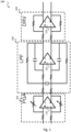
- a typical DC coupled Analog baseband chain 100 is depicted in Fig. 1 .
- the signal is amplified by a Programmable Gain Amplifier (PGA) 101, filtered by the Low Pass Filter (LPF) 102 and then transferred to the Driver (DRV) 103.
- the active blocks are obtained with a closed loop DC coupled voltage amplifier or operational amplifier (OPAMP) 111, 112, 113. Key specifics of an OPAMP are noise, linearity and power consumption.
- the useful signal contains also the DC component
- the DC common mode has to be propagated along the chain and each of the blocks of the chain (PGA 101, LPF 102 and DRV 103) needs to comply with this DC common mode. This is also valid for the OPAMP 111, 112, 113 used in the analog blocks.
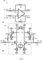
- FIG. 2a an analog PGA 200 is shown ( Fig. 2a ) together with its OPAMP 201 ( Fig. 2b ).
- This PGA 200 is an implementation of the PGA 101 shown in Fig. 1 . Note that the need to have an OPAMP with low output impedance dictates the use of a voltage follower as output stage.
- the PGA 200 includes an operational amplifier 201 having a first (non-inverse, +) input VIN+, a second (inverse, -) input VIN-, a first (non-inverse, +) output VOUT+, a second (inverse, -) output VOUT-.
- a first feedback path including resistor R2 is coupled between output VOUT+ and input VIN+.
- a second feedback path including resistor R2 is coupled between output VOUT- and input VIN-.
- the first input VIN+ of OPAMP 201 is coupled via resistor R1 to a first input VC_IN+ of PGA 200.
- the second input VIN- of OPAMP 201 is coupled via resistor R1 to a second input VC_IN- of PGA 200.
- the first output VOUT+ of OPAMP 201 is the first output of PGA 200.
- the second output VOUT- of OPAMP 201 is the second output of PGA 200.
- the OPAMP 201 includes a non-inverse input path between a drive voltage VDD and ground GND including a first (non-inverse) current source MP+, a first (non-inverse) transistor Q1+ and a second current source Io.
- a control terminal of Q1+ is coupled to the first input VIN+ of the OPAMP 201.
- the OPAMP 201 includes a non-inverse output path between a drive voltage VDD and ground GND including a second (non-inverse) transistor QF+ and a third current source lout.
- a control terminal of QF+ is coupled to a first (non-inverse) internal node Vx+ of the OPAMP 201 which is located between MP+ and Q1+.
- a first terminal of QF+ is coupled to the first output VOUT+ of the OPAMP 201.
- a second terminal of QF+ is coupled to the drive voltage VDD.
- the OPAMP 201 further includes an inverse input path between a drive voltage VDD and ground GND including a first (inverse) current source MP-, a first (inverse) transistor Q1- and a second current source Io.
- a control terminal of Q1- is coupled to the second input VIN- of the OPAMP 201.
- the OPAMP 201 includes an inverse output path between a drive voltage VDD and ground GND including a second (inverse) transistor QF- and a third current source lout.
- a control terminal of QF- is coupled to a first (inverse) node Vx-of the OPAMP 201 which is located between MP- and Q1-.
- a first terminal of QF- is coupled to the second output VOUT- of the OPAMP 201.
- a second terminal of QF- is coupled to the drive voltage VDD.
- a capacitance Cs and a resistor Rs are coupled in parallel between the first terminal of Q1 + and the first terminal of Q1 -.
- the OPAMP 201 can be realized as a differential OPAMP as depicted in Fig. 2 or alternatively as a non-differential OPAMP.
- the non-differential OPAMP 201 has only one first current source MP, one first transistor Q1, one second current source Io, one third current source lout, one input and one output without the differentiation of non-inverse and inverse components.
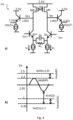
- FIG 3 is a circuit diagram of the OPAMP 201 shown in Figures 1 and 2a /b.
- the OPAMP 201 can be used in the Low Pass Filter 102 shown in Figure 1 or more generally in a closed loop system like for example PGA or DRV, e.g. PGA 101 or DRV 103 as shown in Figure 1 .
- Vn IN 2 4 KT ⁇ 1 g m 1 2 Q 1 g m Q 1 1 + g m 1 Q 1 ⁇ Rs + 1 Rs + 2 ⁇ Io Vov M P
- gm(Q1) is the transconductance of transistor Q1
- Io is the bias current
- OPAMP 201 will be linear until MP acts as a current mirror, i.e. MP stays in the saturation region. This condition is met with Vds(MP)>Vov(MP). Since Vds(MP) will be set by maximum signal level, this means that linearity is maximized if Vov(MP) is minimized.
- EP 0 414 328 A1 concerns a differential amplifier with capacitive coupling disclosing the preamble of claim 1. Another differential amplifier is described in US Patent 3 401 350 . Further prior art is described in Lysenko et al.: A BROADBAND OSCILLOSCOPE AMPLIFIER FOR THE NANOSECOND RANGE, Instruments and Experimental Techniques, Consultant Bureau, New York, US, vol 16., no. 4, July 1, 1973, pages 1173-1175 .
- a basic idea of the invention is to that a DC voltage drop is generated across 1 st and 2 nd stage of an OPAMP to increase linearity.
- optimum DC biasing points for the 1 st and 2 nd stage can be achieved. This maximizes the linearity under a given supply voltage.
- phase margin of the OPAMP is improved.
- the invention relates to a circuit according to claim 1, specifically comprising: a circuit input; a circuit output; at least one passive feedback loop coupled between the circuit output and the circuit input; an active element, in particular a DC coupled operational amplifier (OPAMP), coupled in a feed-forward path of the circuit between the circuit input and the circuit output and configured to drive the at least one feedback loop in order to establish a function of the circuit, wherein the feed-forward path of the circuit comprises a second node and a first node which are internal nodes of the active element and which are coupled between the circuit input and the circuit output, wherein the first node is configured to have a first voltage, the first voltage being a function of the circuit output, wherein the active element comprises a first voltage drop element coupled between the second node and the first node, and wherein the first voltage drop element is configured to decouple a DC level at the first node from a DC level at the second node and configured to provide the DC level at the first node independently from the DC level at the second node
- OPAMP DC
- an improved amplifier circuit design can be provided having increased linearity for DC common mode.
- Such a circuit provides the following advantages: 1) Since optimum DC points for the 1 st and 2 nd stages can be independently chosen, linearity is maximised. 2) Higher flexibility in accommodating differences in DC common mode of preceding / following stages. 3) Higher Gain*Bandwidth Product, since the additional zero can cancel out secondary high frequency poles, therefore improving phase margin. 4) Control of OPAMP performances vs. temperature by using suitable thermal coefficients for Rb and current generator. 5) Reduction of noise performances under certain conditions.
- the first voltage drop element is adjustable and configured to provide an adjustable voltage drop between first node and the second node.
- the first voltage drop element comprises: a voltage drop resistor and a voltage drop capacitor coupled in parallel between the first node and the second node; and a first current source coupled to the first node.
- Such a voltage drop element can be easily implemented in a chip design.
- the voltage drop element creates a voltage drop between the 1 st and the 2 nd stage of the active element, e.g. an OPAMP.
- the voltage drop resistor and the current generator allow one to increase the overdrive voltage of the current generator, thus reducing equivalent input noise.
- the voltage drop generated by the voltage drop resistor and the current generator allows one to optimize separately the 1 st and the 2 nd stage DC operating point; hence a higher linearity can be achieved.
- the first current source is configured to generate a current flowing into the first node such that a DC voltage at the first node is higher than a DC voltage at the second node.
- the first current source is configured to generate a current flowing out of the first node such that a DC voltage at the first node is lower than a DC voltage at the second node.
- the active element comprises: a first transistor coupled to a first input terminal of the active element; and a second transistor coupled to a first output terminal of the active element, wherein the first transistor is coupled via the at least one feedback loop to the second transistor.
- Such a transistor design can be easily implemented, e.g. by bipolar or FET transistor technology.
- the first transistor comprises a first terminal, a second terminal and a control terminal, wherein said control terminal is coupled to the first input terminal of the active element, the second transistor comprises a first terminal, a second terminal and a control terminal, wherein the said first terminal is coupled to the first output terminal of the active element; and the control terminal is coupled to the first node.
- Such a transistor design can be efficiently implemented, e.g. by bipolar or FET transistor technology.
- the voltage drop resistor and the voltage drop capacitor are configured to introduce a zero into a transfer function of the active element.
- the zero in the transfer function stabilizes the circuit. This zero improves phase margin and allows to increase Gain*Bandwidth product.
- a thermal coefficient of the first current source is positive in order to keep a voltage at the second node approximately constant with temperature.
- the circuit comprises a coupling circuit coupled between the first node and the second terminal of the first transistor, wherein the coupling circuit comprises at least the voltage drop resistor and the voltage drop capacitor connected in parallel.
- Such a coupling circuit can be easily implemented in a chip design.
- the active element comprises: a fourth current source coupled between the second terminal of the first transistor and a supply voltage.
- Such an active element can be easily implemented by using only a small number of electronic components.
- the active element further comprises a load capacitance coupled between a supply voltage and the second terminal of the first transistor.
- Such a load capacitance can be used for phase margin of the OPAMP.
- the active element is a differential voltage active element, further comprising: a third transistor coupled to a differential first input terminal of the active element; a fourth transistor coupled to a differential first output terminal of the active element; and a second voltage drop element corresponding to the first voltage drop element, wherein the third transistor is coupled via the second voltage drop element to the fourth transistor.
- a differential voltage active element provides improved linearity.
- the active element further comprises a cascode circuit coupled between the second terminal of the first transistor and the second terminal of the third transistor.
- a cascode circuit provides the advantage of decoupling of the inverse and non-inverse parts resulting in improved linearity and stability.
- the invention relates to an analog baseband circuit, comprising: a programmable gate array (PGA); a low pass filter (LPF) and a driver (DRV), which are DC coupled in series, wherein each of the PGA, LPF and DRV comprises a circuit according to the first aspect as such or any one of the preceding implementation forms of the first aspect.
- PGA programmable gate array
- LPF low pass filter
- DRV driver
- a circuit according to the first aspect as such or any one of the implementation forms of the first aspect can be used, in particular by using a first voltage drop element according to the first aspect as such or any one of the implementation forms of the first aspect.
- Such a method allows to increase linearity of an OPAMP, to increase Gain*Bandwidth product of an OPAMP and to reduce noise of an OPAMP.
- the method may be implemented with a resistance Rb, a capacitance Cb in parallel to Rb and a current generator Mb that create a voltage drop between the 1 st and the 2 nd stage of the OPAMP.
- the voltage drop generated by Rb and the current generator Mb allows one to optimize separately the 1 st and the 2 nd stage DC operating point; hence a higher linearity can be achieved.
- the resistance Rb and capacitance Cb arrangement synthesize a zero in the OPAMP closed loop transfer function. This zero improves phase margin and allows to increase Gain*Bandwidth product.
- Rb and the current generator allow one to increase the overdrive voltage of the current generator MP, thus reducing equivalent input noise.
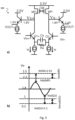
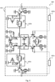
- Fig. 6 shows a circuit diagram illustrating a circuit 600 according to the disclosure in a first implementation form.
- the circuit 600 includes an active element 601 that may correspond to the OPAMP 201 described above with respect to Figures 1 to 5 .
- the active element 601 is coupled in a feed-forward path of the circuit 600 between a circuit input VIN+, VIN- and a circuit output VOUT-, VOUT+.
- At least one feedback path 602a, 602 is coupled between the circuit output VOUT-, VOUT+ and the circuit input VIN+, VIN-.
- the feedback paths 602a, 602b may be realized as described above with respect to Fig. 1 .
- the active element 601 additionally includes one or more voltage drop elements 603a, 603b in a feed-forward path of the active element 601 for decoupling a DC level at first node Vy from a DC level at a second node Vx of the active element 601 and to provide the DC level at the first node Vy independently from the DC level at the second node Vx.
- the active element 601 includes a non-inverse input VIN+ and an inverse input VIN-which are inputs of the circuit 600 and a non-inverse output VOUT+ and an inverse output VOUT- which are outputs of the circuit 600.
- a first feedback path 602a may include a resistor R2 coupled between output VOUT+ and input VIN+, e.g. as described above with respect to Fig. 2a .
- a second feedback path 602b may include a resistor R2 coupled between output VOUT- and input VIN-, e.g. as described above with respect to Fig. 2a .
- the first input VIN+ of the active element 601 may be coupled via resistor R1 to a first input VC_IN+ of the circuit 600, e.g. as described above with respect to Fig. 2a .
- the second input VIN- of the active element 601 may be coupled via resistor R1 to a second input VC_IN- of the circuit 600, e.g. as described above with respect to Fig. 2a .
- the active element 601 includes a non-inverse input path between a drive voltage VDD and ground GND including a first (non-inverse) current source MP+, a first (non-inverse) transistor Q1+ and a second current source Io.
- a control terminal of Q1+ is coupled to the first input VIN+ of the active element 601.
- the active element 601 includes a non-inverse output path between a drive voltage VDD and ground GND including a second (inverse) transistor QF- and a third current source lout.
- a control terminal of QF- forms a first (inverse) internal node Vy- and is coupled via the first voltage drop element 603a to a second (inverse) internal node Vx- of the active element 601 which is located between MP+ and Q1+.
- a first terminal of QF- is coupled to the second output VOUT- of the active element 601.
- a second terminal of QF- is coupled to the drive voltage VDD.
- the non-inverse input path and the non-inverse output path are coupled by a first voltage drop element 603a which is included between first (inverse) internal node Vy- and second (inverse) internal node Vx- which is located at the control terminal of QF-.
- the first voltage drop element 603a includes a parallel circuit of a capacitance Cb and a resistor Rb coupled between the first (inverse) internal node Vy- and the second (inverse) internal node Vx- and a (non-inverse) current source MB+ which is coupled between the first (inverse) internal node Vy- and ground GND.
- the active element 601 further includes an inverse input path between a drive voltage VDD and ground GND including a first (inverse) current source MP-, a first (inverse) transistor Q1- and a second current source Io.
- a control terminal of Q1- is coupled to the second input VIN- of the active element 601.
- the active element 601 includes an inverse output path between a drive voltage VDD and ground GND including a second (non-inverse) transistor QF+ and a third current source lout.
- a control terminal of QF+ forms a first (non-inverse) internal node Vy+ and is coupled via the second voltage drop element 603b to a second (non-inverse) internal node Vx+ of the active element 601 which is located between MP- and Q1-.
- a first terminal of QF+ is coupled to the first output VOUT+ of the active element 601.
- a second terminal of QF+ is coupled to the drive voltage VDD.
- the inverse input path and the inverse output path are coupled by the second voltage drop element 603b which is included between first (non-inverse) internal node Vy+ and second (non-inverse) internal node Vx+ which is located at the control terminal of QF+.
- the second voltage drop element 603b includes a parallel circuit of a capacitance Cb and a resistor Rb coupled between the first (non-inverse) internal node Vy+ and the second (non-inverse) internal node Vx+ and an (inverse) current source MB- which is coupled between the first (non-inverse) internal node Vy+ and ground GND.
- a capacitance Cs and a resistor Rs are coupled in parallel between the first terminal of Q1 + and the first terminal of Q1 -.
- the active element 601 can be realized as a differential OPAMP as depicted in Fig. 6 or alternatively as a non-differential OPAMP.
- the non-differential OPAMP 601 has only one first current source MP, one first transistor Q1, one second current source Io, one third current source lout, one voltage drop element, one input and one output without the differentiation of non-inverse and inverse components.
- the first and/or second transistors Q1+, Q1-, QF+, QF- may be realized as bipolar transistors; in this case the control terminal is a base terminal, the first terminal is an emitter terminal and the second terminal is a collector terminal.
- the first and/or second transistors Q1+, Q1-, QF+, QF- may be realized as Field Effect transistors; in this case the control terminal is a gate terminal, the first terminal is a source terminal and the second terminal is a drain terminal.
- the active element 601 can be realized as a differential active element or alternatively as a non-differential active element.
- the differential active element is shown in Fig. 6 while a non-differential active element comprises of half the elements as depicted in Fig. 6 , i.e. one first current source MP, one first transistor Q1, one second current source lin, one third current source lout, one input and one output without the differentiation of non-inverse and inverse components.
- the circuit 600 includes: a circuit input VIN; a circuit output VOUT; at least one passive feedback loop 602a, 602b coupled between the circuit output and the circuit input; an active element 601, in particular a DC coupled operational amplifier (OPAMP), coupled in a feed-forward path of the circuit 600 between the circuit input and the circuit output and configured to drive the at least one feedback loop in order to establish a function of the circuit.
- the feed-forward path of the circuit 600 comprises a second node Vx and a first node Vy which are internal nodes of the active element 601 and which are coupled between the circuit input and the circuit output.
- the first node Vy is configured to have a first voltage, the first voltage being a function of the circuit output.
- the active element 601 comprises a first voltage drop element 603a coupled between the second node Vx and the first node Vy.
- the first voltage drop element 603a is configured to decouple a DC level at the first node from a DC level at the second node and configured to provide the DC level at the first node independently from the DC level at the second node Vx.
- the first voltage drop element 603a may be adjustable and configured to provide an adjustable voltage drop between first node Vy and the second node Vx.
- the first voltage drop element 603a may include: a voltage drop resistor Rb and a voltage drop capacitor Cb coupled in parallel between the first node Vy and the second node Vx; and a first current source Mb coupled to the first node Vy.
- the first current source Mb may generate a current Io flowing into the first node Vy such that a DC voltage at the first node Vy is higher than a DC voltage at the second node Vx.
- the first current source Mb may generate a current flowing out of the first node Vy such that a DC voltage at the first node Vy is lower than a DC voltage at the second node Vx.
- the voltage drop resistor Rb and the voltage drop capacitor Cb may be configured to introduce a zero into a transfer function of the active element 601.
- a thermal coefficient of the first current source Mb may be positive in order to keep a voltage at the second node Vx approximately constant with temperature.
- the active element 601 may include: a first transistor Q1+ coupled to a first input terminal Vin+ of the active element 601; and a second transistor QF- coupled to a first output terminal Vout- of the active element 601.
- the first transistor Q1 + may be coupled via the at least one feedback loop 602a to the second transistor QF-.
- the first transistor Q1+ may include a first terminal, a second terminal and a control terminal. Said control terminal may be coupled to the first input terminal Vin+ of the active element 601.
- the second transistor QF- may include a first terminal, a second terminal and a control terminal. Said first terminal may be coupled to the first output terminal Vout-of the active element 601.
- the control terminal may be coupled to the first node Vy.
- the circuit 600 may further include a coupling circuit coupled between the first node Vy and the second terminal of Q1+.
- the coupling circuit may include at least the voltage drop resistor Rb and the voltage drop capacitor Cb connected in parallel.
- the active element 601 may include: a second current source MP+ coupled between the second terminal of Q1+ and a supply voltage; a third current source Io coupled between the first terminal of Q1+ and a ground terminal; and a fourth current source lout coupled between the first terminal of QF- and a ground terminal.
- the active element 601 may further include a load capacitance Cp coupled between a supply voltage and the second terminal of Q1+.
- the active element 601 may be a differential voltage active element, further including: a third transistor Q1- coupled to a differential first input terminal Vin- of the active element; a fourth transistor QF+ coupled to a differential first output terminal Vout+ of the active element; and a second voltage drop element corresponding to the first voltage drop element.
- the third transistor Q1- may be coupled via the second voltage drop element to the fourth transistor QF+.
- the active element 601 may further include a cascode circuit coupled between the second terminal of Q1+ and the second terminal of Q1-.
- the circuit 600 may be used in an analog baseband circuit, e.g. an analog baseband circuit 100 as described above with respect to Fig. 1 .
- the analog baseband circuit 100 may include a programmable gate array (PGA) 101; a low pass filter (LPF) 102 and a driver (DRV) 103, which are DC coupled in series, wherein each of the PGA 101, LPF 102 and DRV 103 comprises a circuit 600 as described above.
- PGA programmable gate array
- LPF low pass filter
- DRV driver
- the circuit 600 solves the above mentioned problems by introducing the voltage drop elements 603a, 603b, i.e. the combination of a resistance Rb, capacitance Cb and an additional current generator.
- the voltage drop elements 603a, 603b act in the following way: 1) Rb and the current generator Mb create a DC voltage drop that optimizes simultaneously the DC operating points for the 1 st and the 2 nd stage. 2) Rb, Cb introduces a zero at high-frequency that improves phase margin of the OPAMP, i.e. the active element 601. 3) Rb and the current generator Mb can have a suitable thermal coefficient in order to provide the desired DC bias point for node Vx. This feature can be used to ensure desired linearity performances for different temperatures. 4) Under certain conditions (high Gain of the OPAMP), the circuit 600 has improved noise performance.
- Rb and the current generator can have a suitable thermal coefficient in order to provide the desired DC bias point for node Vx. This feature can be used to ensure desired linearity performances for different temperatures. An example is reported below.
- the circuit 600 allows a temperature control of the DC voltage at node Vx in order to provide desired performances versus temperature.
- V IN 2 4 KT ⁇ 1 g Q 1 m 1 2 g m Q 1 1 + g m 1 Q 1 ⁇ Rs + 1 Rs + 2 ⁇ Io Vov M P .
- V IN 2 4 KT ⁇ 1 g Q 1 m 1 2 g m Q 1 1 + g m 1 Q 1 ⁇ Rs + 1 Rs + 2 ⁇ Io ⁇ 1 ⁇ ⁇ Vov M P + 2 ⁇ Io ⁇ ⁇ Vov M P .
- Vov(MP) of circuit 600 can be made bigger than Vov(MP) of circuit 300 due to more hadroom available for transistor MP ( thanks to the DC voltage drop), it results that Vinv IN ⁇ V IN . In conclusion, under certain conditions, the disclosed circuit 600 yields also better noise performances.
- the circuit 600 provides the following advantages: Since optimum DC points for the 1 st and 2 nd stages can be independently chosen, linearity is maximised; Higher flexibility in accommodating differences in DC common mode of preceding / following stages; Higher Gain*Bandwidth Product, since the additional zero can cancel out secondary high frequency poles, therefore improving phase margin; Control of OPAMP performances versus temperature by using suitable thermal coefficients for Rb and current generator; and reduction of noise performances under certain conditions.
- Fig. 7 shows a circuit diagram illustrating a circuit 700 according to the disclosure in a second implementation form.
- the circuit 700 corresponds to the circuit 600 described above with respect to Fig. 6 ; however the current sources MB+, MB- of the voltage drop elements 603a, 603b are not coupled to the reference voltage VDD, instead MB+ and MB- are coupled to ground GND.
- These different voltage drop elements used for the circuit 700 are referred to as 703a and 703b.
Landscapes
- Engineering & Computer Science (AREA)
- Power Engineering (AREA)
- Physics & Mathematics (AREA)
- Nonlinear Science (AREA)
- Amplifiers (AREA)
Claims (9)
- Schaltung (600), die umfasst:einen Schaltungseingang (VIN);einen Schaltungsausgang (VOUT);mindestens eine passive Rückkopplungsschleife (602a, 602b), die zwischen dem Schaltungsausgang (VOUT) und dem Schaltungseingang (VIN) gekoppelt ist;ein aktives Element (601), insbesondere einen Gleichstrom-gekoppelten Operationsverstärker (OPAMP), der in einem Vorwärtskopplungsweg der Schaltung (600) zwischen dem Schaltungseingang (VIN) und dem Schaltungsausgang (VOUT) gekoppelt und konfiguriert ist, um die mindestens eine Rückkopplungsschleife anzutreiben, um eine Funktion der Schaltung herzustellen,wobei das aktive Element (601) einen Eingangsweg zwischen einer Antriebsspannung (VDD) und einer Masse (GND), der eine erste Stromquelle (MP), einen ersten Transistor (Q1) und eine zweite Stromquelle (Io) einschließt, und einen Ausgangsweg zwischen der Antriebsspannung (VDD) und der Masse (GND) einschließt, der einen zweiten Transistor (QF) und eine dritte Stromquelle (lout) einschließt, wobei ein Steueranschluss des ersten Transistors (Q1) mit dem Schaltungseingang (VIN) gekoppelt ist und ein erster Anschluss des zweiten Transistors (QF) mit dem Schaltungsausgang (VOUT) gekoppelt ist; wobei der Vorwärtskopplungsweg der Schaltung einen zweiten Knoten (Vx) und einen ersten Knoten (Vy), die interne Knoten des aktiven Elements (600) sind, umfasst, wobei ein Steueranschluss des zweiten Transistors (QF) der erste Knoten (Vy) ist;wobei der erste Knoten (Vy), direkt oder über einen Kaskadentransistor (Q2), mit einem zweiten Anschluss des ersten Transistors (Q1) gekoppelt ist, wobei der erste Knoten (Vy) konfiguriert ist, um eine erste Spannung aufzuweisen, wobei eine Spannung des Schaltungsausgangs (VOUT) von der ersten Spannung abhängig ist, dadurch gekennzeichnet, dass das aktive Element (601) ein erstes Spannungsabfallelement (603a, 603b), das zwischen dem zweiten Knoten (Vx) und dem ersten Knoten (Vy) gekoppelt ist, umfasst undwobei das erste Spannungsabfallelement (603a, 603b) einstellbar und konfiguriert ist, um einen einstellbaren Spannungsabfall zwischen dem ersten Knoten (Vy) und dem zweiten Knoten (Vx) bereitzustellen, um einen Gleichstrompegel an dem ersten Knoten von einem Gleichstrompegel an dem zweiten Knoten (Vx) zu entkoppeln und den Gleichstrompegel an dem ersten Knoten (Vy) unabhängig von dem Gleichstrompegel an dem zweiten Knoten (Vx) bereitzustellen; wobei das erste Spannungsabfallelement (603a, 603b) umfasst:einen Spannungsabfallwiderstand (Rb) und einen Spannungsabfallkondensator (Cb), der parallel zwischen dem ersten Knoten und dem zweiten Knoten gekoppelt ist;wobei eine erste Stromquelle (Mb) konfiguriert ist, um einen Strom, der in den ersten Knoten fließt, derart zu erzeugen, dass eine Gleichstromspannung an dem ersten Knoten höher als eine Gleichstromspannung an dem zweiten Knoten ist; undwobei die erste Stromquelle (Mb) konfiguriert ist, um einen Strom, der aus dem ersten Knoten fließt, derart zu erzeugen, dass eine Gleichstromspannung an dem ersten Knoten niedriger als eine Gleichstromspannung an dem zweiten Knoten ist.
- Schaltung (600) nach Anspruch 1, wobei der Spannungsabfallwiderstand (Rb) und der Spannungsabfallkondensator (Cb) konfiguriert sind, um eine Null in eine Übertragungsfunktion des aktiven Elements einzuführen.
- Schaltung (600) nach Anspruch 1 oder 2, wobei ein thermischer Koeffizient der ersten Stromquelle (Mb) positiv ist, um eine Spannung an dem zweiten Knoten (Vx) ungefähr konstant mit der Temperatur zu halten.
- Schaltung (600) nach einem der Ansprüche 1 bis 3, die umfasst:
eine Kopplungsschaltung, die zwischen dem ersten Knoten und dem zweiten Anschluss des ersten Transistors (Q1) gekoppelt ist, wobei die Kopplungsschaltung mindestens den Spannungsabfallwiderstand (Rb) und den Spannungsabfallkondensator (Cb), die parallel verbunden sind, umfasst. - Schaltung (600) nach einem der Ansprüche 1 bis 4, wobei das aktive Element (OPAMP) umfasst:
eine vierte Stromquelle (MP+), die zwischen dem zweiten Anschluss von Q1+ und einer Versorgungsspannung gekoppelt ist. - Schaltung (600) nach einem der Ansprüche 1 bis 5, wobei das aktive Element (OPAMP) ferner umfasst:
eine Lastkapazität (Cp), die zwischen einer Versorgungsspannung und dem zweiten Anschluss von Q1+ gekoppelt ist. - Schaltung (600) nach einem der Ansprüche 1 bis 6, wobei das aktive Element (OPAMP) ein aktives Differenzspannungselement ist, das ferner umfasst:einen dritten Transistor (Q1-), der mit einem ersten Differenzeingangsanschluss (Vin-) des aktiven Elements gekoppelt ist;einen vierten Transistor (QF+), der mit einem ersten Differenzausgangsanschluss (Vout+) des aktiven Elements gekoppelt ist; undein zweites Spannungsabfallelement, das dem ersten Spannungsabfallelement entspricht,wobei der dritte Transistor (Q1-) über das zweite Spannungsabfallelement mit dem vierten Transistor (QF+) gekoppelt ist.
- Schaltung (600) nach Anspruch 7, wobei das aktive Element (OPAMP) ferner umfasst:
eine Kaskodenschaltung, die zwischen dem zweiten Anschluss von Q1+ und dem zweiten Anschluss von Q1- gekoppelt ist. - Analoge Basisbandschaltung (100), die umfasst:ein programmierbares Gate-Array (PGA) (101);einen Tiefpassfilter (LPF) (102); undeinen Antrieb (DRV) (103), der in Reihe Gleichstrom-gekoppelt ist,wobei jedes des PGA, LPF und DRV eine Schaltung (600) nach einem der vorstehenden Ansprüche umfasst.
Applications Claiming Priority (1)
| Application Number | Priority Date | Filing Date | Title |
|---|---|---|---|
| PCT/EP2016/060771 WO2017194143A1 (en) | 2016-05-12 | 2016-05-12 | Circuit with voltage drop element |
Publications (2)
| Publication Number | Publication Date |
|---|---|
| EP3314756A1 EP3314756A1 (de) | 2018-05-02 |
| EP3314756B1 true EP3314756B1 (de) | 2024-07-31 |
Family
ID=55967298
Family Applications (1)
| Application Number | Title | Priority Date | Filing Date |
|---|---|---|---|
| EP16722235.5A Active EP3314756B1 (de) | 2016-05-12 | 2016-05-12 | Schaltung mit spannungsabfallelement |
Country Status (5)
| Country | Link |
|---|---|
| US (1) | US10454430B2 (de) |
| EP (1) | EP3314756B1 (de) |
| KR (1) | KR102057473B1 (de) |
| CN (2) | CN109075746B (de) |
| WO (1) | WO2017194143A1 (de) |
Citations (2)
| Publication number | Priority date | Publication date | Assignee | Title |
|---|---|---|---|---|
| EP0414328B1 (de) * | 1989-08-25 | 1995-01-04 | Philips Composants | Differenzverstärker mit Kondensatorkopplung |
| US6184919B1 (en) * | 1994-01-05 | 2001-02-06 | Robert R. Asprey | Extended length differentially driven analog video link |
Family Cites Families (20)
| Publication number | Priority date | Publication date | Assignee | Title |
|---|---|---|---|---|
| US3077566A (en) * | 1961-06-01 | 1963-02-12 | Mouroe Electronies Inc | Transistor operational amplifier |
| US3401350A (en) * | 1965-03-22 | 1968-09-10 | Monsanto Co | Differential amplifier |
| JPS603218A (ja) | 1983-06-21 | 1985-01-09 | Sony Corp | トランジスタアンプ |
| US5463345A (en) * | 1993-01-07 | 1995-10-31 | Nec Corporation | Circuit for converting unipolar input to bipolar output |
| US6583662B1 (en) * | 1999-06-23 | 2003-06-24 | Globespanvirata, Inc. | Circuit and method for implementing an integrated continuous-time smoothing filter |
| US6288609B1 (en) | 2000-02-29 | 2001-09-11 | Motorola, Inc. | Gain controllable low noise amplifier with automatic linearity enhancement and method of doing same |
| DE10064207A1 (de) * | 2000-12-22 | 2002-07-11 | Infineon Technologies Ag | Schaltungsanordnung zur rauscharmen volldifferenziellen Verstärkung |
| US7535280B2 (en) * | 2004-04-30 | 2009-05-19 | Texas Instruments Incorporated | Apparatus and method for shifting a signal from a first reference level to a second reference level |
| US7298210B2 (en) * | 2005-05-24 | 2007-11-20 | Texas Instruments Incorporated | Fast settling, low noise, low offset operational amplifier and method |
| CN101266506B (zh) * | 2007-03-16 | 2010-12-01 | 深圳赛意法微电子有限公司 | Cmos工艺中无运算放大器的带隙基准电压源 |
| US7898278B2 (en) * | 2007-11-05 | 2011-03-01 | Arm Limited | Power control circuitry, circuitry for analysing a switched power rail, and method of controlling connection of a power source to a switched power rail |
| US7889006B1 (en) | 2009-09-23 | 2011-02-15 | Maxim Integrated Products, Inc. | dB-linear process-independent variable gain amplifier |
| US8558611B2 (en) * | 2012-02-14 | 2013-10-15 | International Business Machines Corporation | Peaking amplifier with capacitively-coupled parallel input stages |
| WO2014124690A1 (en) * | 2013-02-15 | 2014-08-21 | Huawei Technologies Co., Ltd. | Lc oscillator with tail current source and transformer-based tank circuit |
| CN103326682A (zh) * | 2013-05-27 | 2013-09-25 | 苏州贝克微电子有限公司 | 具有高线性度的可调运算跨导放大器 |
| US9391577B2 (en) | 2014-05-07 | 2016-07-12 | Linear Technology Corporation | Low-voltage analog variable gain amplifier with enhanced linearity |
| US9720020B2 (en) * | 2014-05-28 | 2017-08-01 | Nxp B.V. | Broad-range current measurement using variable resistance |
| US9628028B2 (en) * | 2014-09-09 | 2017-04-18 | Stmicroelectronics S.R.L. | Common-mode feedback circuit, corresponding signal processing circuit and method |
| CN104793690A (zh) * | 2015-04-27 | 2015-07-22 | 西安电子科技大学 | 一种高精度带隙基准源 |
| CN205945697U (zh) * | 2016-06-24 | 2017-02-08 | 深圳市炬烜科技有限公司 | 一种基于恒温技术和温度补偿技术新型小体积高稳晶体振荡器 |
-
2016
- 2016-05-12 KR KR1020187004029A patent/KR102057473B1/ko active Active
- 2016-05-12 CN CN201680085575.5A patent/CN109075746B/zh active Active
- 2016-05-12 EP EP16722235.5A patent/EP3314756B1/de active Active
- 2016-05-12 CN CN202110701850.4A patent/CN113810000A/zh active Pending
- 2016-05-12 WO PCT/EP2016/060771 patent/WO2017194143A1/en not_active Ceased
-
2018
- 2018-03-02 US US15/910,554 patent/US10454430B2/en active Active
Patent Citations (2)
| Publication number | Priority date | Publication date | Assignee | Title |
|---|---|---|---|---|
| EP0414328B1 (de) * | 1989-08-25 | 1995-01-04 | Philips Composants | Differenzverstärker mit Kondensatorkopplung |
| US6184919B1 (en) * | 1994-01-05 | 2001-02-06 | Robert R. Asprey | Extended length differentially driven analog video link |
Also Published As
| Publication number | Publication date |
|---|---|
| US20180198421A1 (en) | 2018-07-12 |
| WO2017194143A1 (en) | 2017-11-16 |
| US10454430B2 (en) | 2019-10-22 |
| CN113810000A (zh) | 2021-12-17 |
| CN109075746A (zh) | 2018-12-21 |
| CN109075746B (zh) | 2021-06-29 |
| KR20180116211A (ko) | 2018-10-24 |
| EP3314756A1 (de) | 2018-05-02 |
| KR102057473B1 (ko) | 2019-12-19 |
Similar Documents
| Publication | Publication Date | Title |
|---|---|---|
| US7576610B2 (en) | Operational amplifier of class AB | |
| US7310016B2 (en) | Chopper-stabilized operational amplifier and method | |
| US6891433B2 (en) | Low voltage high gain amplifier circuits | |
| US20060091952A1 (en) | High-swing folded cascode having a novel gain-boost amplifier | |
| US6833760B1 (en) | Low power differential amplifier powered by multiple unequal power supply voltages | |
| KR101333421B1 (ko) | 저전압 저전력 a/b급 출력단 | |
| US7248117B1 (en) | Frequency compensation architecture for stable high frequency operation | |
| US20080197928A1 (en) | Threshold voltage compensation for a two stage amplifier | |
| JP7001468B2 (ja) | オペアンプ | |
| US6731165B1 (en) | Electronic amplifier | |
| US9231540B2 (en) | High performance class AB operational amplifier | |
| US7295071B1 (en) | High speed, high DC gain and wide dynamic range amplifier | |
| EP3314756B1 (de) | Schaltung mit spannungsabfallelement | |
| KR100574969B1 (ko) | 향상된 이득을 가지는 조절된 캐스코드 증폭 회로 | |
| US5023567A (en) | Stability-compensated operational amplifier | |
| US20030058044A1 (en) | Amplifier improvements | |
| EP2218176B1 (de) | Rauscharmer verstärker | |
| US20020005757A1 (en) | Fully differential operational amplifier of the folded cascode type | |
| JP4867066B2 (ja) | 増幅回路 | |
| US6831501B1 (en) | Common-mode controlled differential gain boosting | |
| US7170337B2 (en) | Low voltage wide ratio current mirror | |
| Pourashraf et al. | A super class-AB OTA with high output current and no open loop gain degradation | |
| US20050057309A1 (en) | Transistor amplifier | |
| US6542034B2 (en) | Operational amplifier with high gain and symmetrical output-current capability | |
| US6930542B1 (en) | Differential gain boosting |
Legal Events
| Date | Code | Title | Description |
|---|---|---|---|
| STAA | Information on the status of an ep patent application or granted ep patent |
Free format text: STATUS: THE INTERNATIONAL PUBLICATION HAS BEEN MADE |
|
| PUAI | Public reference made under article 153(3) epc to a published international application that has entered the european phase |
Free format text: ORIGINAL CODE: 0009012 |
|
| STAA | Information on the status of an ep patent application or granted ep patent |
Free format text: STATUS: REQUEST FOR EXAMINATION WAS MADE |
|
| 17P | Request for examination filed |
Effective date: 20180127 |
|
| AK | Designated contracting states |
Kind code of ref document: A1 Designated state(s): AL AT BE BG CH CY CZ DE DK EE ES FI FR GB GR HR HU IE IS IT LI LT LU LV MC MK MT NL NO PL PT RO RS SE SI SK SM TR |
|
| AX | Request for extension of the european patent |
Extension state: BA ME |
|
| DAV | Request for validation of the european patent (deleted) | ||
| DAX | Request for extension of the european patent (deleted) | ||
| STAA | Information on the status of an ep patent application or granted ep patent |
Free format text: STATUS: EXAMINATION IS IN PROGRESS |
|
| 17Q | First examination report despatched |
Effective date: 20210412 |
|
| GRAP | Despatch of communication of intention to grant a patent |
Free format text: ORIGINAL CODE: EPIDOSNIGR1 |
|
| STAA | Information on the status of an ep patent application or granted ep patent |
Free format text: STATUS: GRANT OF PATENT IS INTENDED |
|
| RIC1 | Information provided on ipc code assigned before grant |
Ipc: H03F 1/30 20060101ALI20240229BHEP Ipc: H03F 3/45 20060101ALI20240229BHEP Ipc: H03F 1/32 20060101AFI20240229BHEP |
|
| INTG | Intention to grant announced |
Effective date: 20240318 |
|
| P01 | Opt-out of the competence of the unified patent court (upc) registered |
Effective date: 20240404 |
|
| GRAS | Grant fee paid |
Free format text: ORIGINAL CODE: EPIDOSNIGR3 |
|
| GRAA | (expected) grant |
Free format text: ORIGINAL CODE: 0009210 |
|
| STAA | Information on the status of an ep patent application or granted ep patent |
Free format text: STATUS: THE PATENT HAS BEEN GRANTED |
|
| AK | Designated contracting states |
Kind code of ref document: B1 Designated state(s): AL AT BE BG CH CY CZ DE DK EE ES FI FR GB GR HR HU IE IS IT LI LT LU LV MC MK MT NL NO PL PT RO RS SE SI SK SM TR |
|
| REG | Reference to a national code |
Ref country code: CH Ref legal event code: EP Ref country code: GB Ref legal event code: FG4D |
|
| REG | Reference to a national code |
Ref country code: DE Ref legal event code: R096 Ref document number: 602016088649 Country of ref document: DE |
|
| REG | Reference to a national code |
Ref country code: IE Ref legal event code: FG4D |
|
| REG | Reference to a national code |
Ref country code: LT Ref legal event code: MG9D |
|
| REG | Reference to a national code |
Ref country code: NL Ref legal event code: MP Effective date: 20240731 |
|
| PG25 | Lapsed in a contracting state [announced via postgrant information from national office to epo] |
Ref country code: PT Free format text: LAPSE BECAUSE OF FAILURE TO SUBMIT A TRANSLATION OF THE DESCRIPTION OR TO PAY THE FEE WITHIN THE PRESCRIBED TIME-LIMIT Effective date: 20241202 |
|
| REG | Reference to a national code |
Ref country code: AT Ref legal event code: MK05 Ref document number: 1709457 Country of ref document: AT Kind code of ref document: T Effective date: 20240731 |
|
| PG25 | Lapsed in a contracting state [announced via postgrant information from national office to epo] |
Ref country code: PT Free format text: LAPSE BECAUSE OF FAILURE TO SUBMIT A TRANSLATION OF THE DESCRIPTION OR TO PAY THE FEE WITHIN THE PRESCRIBED TIME-LIMIT Effective date: 20241202 |
|
| PG25 | Lapsed in a contracting state [announced via postgrant information from national office to epo] |
Ref country code: NO Free format text: LAPSE BECAUSE OF FAILURE TO SUBMIT A TRANSLATION OF THE DESCRIPTION OR TO PAY THE FEE WITHIN THE PRESCRIBED TIME-LIMIT Effective date: 20241031 |
|
| PG25 | Lapsed in a contracting state [announced via postgrant information from national office to epo] |
Ref country code: PL Free format text: LAPSE BECAUSE OF FAILURE TO SUBMIT A TRANSLATION OF THE DESCRIPTION OR TO PAY THE FEE WITHIN THE PRESCRIBED TIME-LIMIT Effective date: 20240731 Ref country code: FI Free format text: LAPSE BECAUSE OF FAILURE TO SUBMIT A TRANSLATION OF THE DESCRIPTION OR TO PAY THE FEE WITHIN THE PRESCRIBED TIME-LIMIT Effective date: 20240731 Ref country code: NL Free format text: LAPSE BECAUSE OF FAILURE TO SUBMIT A TRANSLATION OF THE DESCRIPTION OR TO PAY THE FEE WITHIN THE PRESCRIBED TIME-LIMIT Effective date: 20240731 Ref country code: GR Free format text: LAPSE BECAUSE OF FAILURE TO SUBMIT A TRANSLATION OF THE DESCRIPTION OR TO PAY THE FEE WITHIN THE PRESCRIBED TIME-LIMIT Effective date: 20241101 |
|
| PG25 | Lapsed in a contracting state [announced via postgrant information from national office to epo] |
Ref country code: BG Free format text: LAPSE BECAUSE OF FAILURE TO SUBMIT A TRANSLATION OF THE DESCRIPTION OR TO PAY THE FEE WITHIN THE PRESCRIBED TIME-LIMIT Effective date: 20240731 |
|
| PG25 | Lapsed in a contracting state [announced via postgrant information from national office to epo] |
Ref country code: LV Free format text: LAPSE BECAUSE OF FAILURE TO SUBMIT A TRANSLATION OF THE DESCRIPTION OR TO PAY THE FEE WITHIN THE PRESCRIBED TIME-LIMIT Effective date: 20240731 |
|
| PG25 | Lapsed in a contracting state [announced via postgrant information from national office to epo] |
Ref country code: IS Free format text: LAPSE BECAUSE OF FAILURE TO SUBMIT A TRANSLATION OF THE DESCRIPTION OR TO PAY THE FEE WITHIN THE PRESCRIBED TIME-LIMIT Effective date: 20241130 Ref country code: AT Free format text: LAPSE BECAUSE OF FAILURE TO SUBMIT A TRANSLATION OF THE DESCRIPTION OR TO PAY THE FEE WITHIN THE PRESCRIBED TIME-LIMIT Effective date: 20240731 |
|
| PG25 | Lapsed in a contracting state [announced via postgrant information from national office to epo] |
Ref country code: HR Free format text: LAPSE BECAUSE OF FAILURE TO SUBMIT A TRANSLATION OF THE DESCRIPTION OR TO PAY THE FEE WITHIN THE PRESCRIBED TIME-LIMIT Effective date: 20240731 |
|
| PG25 | Lapsed in a contracting state [announced via postgrant information from national office to epo] |
Ref country code: ES Free format text: LAPSE BECAUSE OF FAILURE TO SUBMIT A TRANSLATION OF THE DESCRIPTION OR TO PAY THE FEE WITHIN THE PRESCRIBED TIME-LIMIT Effective date: 20240731 Ref country code: RS Free format text: LAPSE BECAUSE OF FAILURE TO SUBMIT A TRANSLATION OF THE DESCRIPTION OR TO PAY THE FEE WITHIN THE PRESCRIBED TIME-LIMIT Effective date: 20241031 |
|
| PG25 | Lapsed in a contracting state [announced via postgrant information from national office to epo] |
Ref country code: RS Free format text: LAPSE BECAUSE OF FAILURE TO SUBMIT A TRANSLATION OF THE DESCRIPTION OR TO PAY THE FEE WITHIN THE PRESCRIBED TIME-LIMIT Effective date: 20241031 Ref country code: PL Free format text: LAPSE BECAUSE OF FAILURE TO SUBMIT A TRANSLATION OF THE DESCRIPTION OR TO PAY THE FEE WITHIN THE PRESCRIBED TIME-LIMIT Effective date: 20240731 Ref country code: NO Free format text: LAPSE BECAUSE OF FAILURE TO SUBMIT A TRANSLATION OF THE DESCRIPTION OR TO PAY THE FEE WITHIN THE PRESCRIBED TIME-LIMIT Effective date: 20241031 Ref country code: NL Free format text: LAPSE BECAUSE OF FAILURE TO SUBMIT A TRANSLATION OF THE DESCRIPTION OR TO PAY THE FEE WITHIN THE PRESCRIBED TIME-LIMIT Effective date: 20240731 Ref country code: LV Free format text: LAPSE BECAUSE OF FAILURE TO SUBMIT A TRANSLATION OF THE DESCRIPTION OR TO PAY THE FEE WITHIN THE PRESCRIBED TIME-LIMIT Effective date: 20240731 Ref country code: IS Free format text: LAPSE BECAUSE OF FAILURE TO SUBMIT A TRANSLATION OF THE DESCRIPTION OR TO PAY THE FEE WITHIN THE PRESCRIBED TIME-LIMIT Effective date: 20241130 Ref country code: HR Free format text: LAPSE BECAUSE OF FAILURE TO SUBMIT A TRANSLATION OF THE DESCRIPTION OR TO PAY THE FEE WITHIN THE PRESCRIBED TIME-LIMIT Effective date: 20240731 Ref country code: GR Free format text: LAPSE BECAUSE OF FAILURE TO SUBMIT A TRANSLATION OF THE DESCRIPTION OR TO PAY THE FEE WITHIN THE PRESCRIBED TIME-LIMIT Effective date: 20241101 Ref country code: FI Free format text: LAPSE BECAUSE OF FAILURE TO SUBMIT A TRANSLATION OF THE DESCRIPTION OR TO PAY THE FEE WITHIN THE PRESCRIBED TIME-LIMIT Effective date: 20240731 Ref country code: ES Free format text: LAPSE BECAUSE OF FAILURE TO SUBMIT A TRANSLATION OF THE DESCRIPTION OR TO PAY THE FEE WITHIN THE PRESCRIBED TIME-LIMIT Effective date: 20240731 Ref country code: BG Free format text: LAPSE BECAUSE OF FAILURE TO SUBMIT A TRANSLATION OF THE DESCRIPTION OR TO PAY THE FEE WITHIN THE PRESCRIBED TIME-LIMIT Effective date: 20240731 Ref country code: AT Free format text: LAPSE BECAUSE OF FAILURE TO SUBMIT A TRANSLATION OF THE DESCRIPTION OR TO PAY THE FEE WITHIN THE PRESCRIBED TIME-LIMIT Effective date: 20240731 |
|
| PG25 | Lapsed in a contracting state [announced via postgrant information from national office to epo] |
Ref country code: RO Free format text: LAPSE BECAUSE OF FAILURE TO SUBMIT A TRANSLATION OF THE DESCRIPTION OR TO PAY THE FEE WITHIN THE PRESCRIBED TIME-LIMIT Effective date: 20240731 Ref country code: SM Free format text: LAPSE BECAUSE OF FAILURE TO SUBMIT A TRANSLATION OF THE DESCRIPTION OR TO PAY THE FEE WITHIN THE PRESCRIBED TIME-LIMIT Effective date: 20240731 Ref country code: DK Free format text: LAPSE BECAUSE OF FAILURE TO SUBMIT A TRANSLATION OF THE DESCRIPTION OR TO PAY THE FEE WITHIN THE PRESCRIBED TIME-LIMIT Effective date: 20240731 |
|
| PG25 | Lapsed in a contracting state [announced via postgrant information from national office to epo] |
Ref country code: EE Free format text: LAPSE BECAUSE OF FAILURE TO SUBMIT A TRANSLATION OF THE DESCRIPTION OR TO PAY THE FEE WITHIN THE PRESCRIBED TIME-LIMIT Effective date: 20240731 |
|
| PG25 | Lapsed in a contracting state [announced via postgrant information from national office to epo] |
Ref country code: CZ Free format text: LAPSE BECAUSE OF FAILURE TO SUBMIT A TRANSLATION OF THE DESCRIPTION OR TO PAY THE FEE WITHIN THE PRESCRIBED TIME-LIMIT Effective date: 20240731 |
|
| PG25 | Lapsed in a contracting state [announced via postgrant information from national office to epo] |
Ref country code: SK Free format text: LAPSE BECAUSE OF FAILURE TO SUBMIT A TRANSLATION OF THE DESCRIPTION OR TO PAY THE FEE WITHIN THE PRESCRIBED TIME-LIMIT Effective date: 20240731 Ref country code: IT Free format text: LAPSE BECAUSE OF FAILURE TO SUBMIT A TRANSLATION OF THE DESCRIPTION OR TO PAY THE FEE WITHIN THE PRESCRIBED TIME-LIMIT Effective date: 20240731 |
|
| REG | Reference to a national code |
Ref country code: DE Ref legal event code: R097 Ref document number: 602016088649 Country of ref document: DE |
|
| PLBE | No opposition filed within time limit |
Free format text: ORIGINAL CODE: 0009261 |
|
| STAA | Information on the status of an ep patent application or granted ep patent |
Free format text: STATUS: NO OPPOSITION FILED WITHIN TIME LIMIT |
|
| 26N | No opposition filed |
Effective date: 20250501 |
|
| PGFP | Annual fee paid to national office [announced via postgrant information from national office to epo] |
Ref country code: DE Payment date: 20250402 Year of fee payment: 10 |
|
| PGFP | Annual fee paid to national office [announced via postgrant information from national office to epo] |
Ref country code: FR Payment date: 20250401 Year of fee payment: 10 |
|
| PG25 | Lapsed in a contracting state [announced via postgrant information from national office to epo] |
Ref country code: SE Free format text: LAPSE BECAUSE OF FAILURE TO SUBMIT A TRANSLATION OF THE DESCRIPTION OR TO PAY THE FEE WITHIN THE PRESCRIBED TIME-LIMIT Effective date: 20240731 |