EP3308971B1 - Papier filigrané - Google Patents
Papier filigrané Download PDFInfo
- Publication number
- EP3308971B1 EP3308971B1 EP16811244.9A EP16811244A EP3308971B1 EP 3308971 B1 EP3308971 B1 EP 3308971B1 EP 16811244 A EP16811244 A EP 16811244A EP 3308971 B1 EP3308971 B1 EP 3308971B1
- Authority
- EP
- European Patent Office
- Prior art keywords
- dimmer
- layer
- paper
- watermarked paper
- watermarked
- Prior art date
- Legal status (The legal status is an assumption and is not a legal conclusion. Google has not performed a legal analysis and makes no representation as to the accuracy of the status listed.)
- Active
Links
- 230000003287 optical effect Effects 0.000 claims description 28
- 230000005540 biological transmission Effects 0.000 claims description 7
- 238000002156 mixing Methods 0.000 claims description 2
- 239000010410 layer Substances 0.000 description 139
- 239000000463 material Substances 0.000 description 61
- 238000000034 method Methods 0.000 description 39
- 239000010408 film Substances 0.000 description 29
- 239000000203 mixture Substances 0.000 description 25
- 239000000976 ink Substances 0.000 description 16
- 229920005989 resin Polymers 0.000 description 16
- 239000011347 resin Substances 0.000 description 16
- 230000008859 change Effects 0.000 description 14
- 238000004544 sputter deposition Methods 0.000 description 11
- 239000012790 adhesive layer Substances 0.000 description 10
- XLYOFNOQVPJJNP-UHFFFAOYSA-N water Substances O XLYOFNOQVPJJNP-UHFFFAOYSA-N 0.000 description 10
- ZWEHNKRNPOVVGH-UHFFFAOYSA-N 2-Butanone Chemical compound CCC(C)=O ZWEHNKRNPOVVGH-UHFFFAOYSA-N 0.000 description 9
- 230000000694 effects Effects 0.000 description 9
- -1 polyethylene terephthalate Polymers 0.000 description 9
- PXHVJJICTQNCMI-UHFFFAOYSA-N Nickel Chemical compound [Ni] PXHVJJICTQNCMI-UHFFFAOYSA-N 0.000 description 8
- 238000007646 gravure printing Methods 0.000 description 8
- 239000002994 raw material Substances 0.000 description 8
- 230000003197 catalytic effect Effects 0.000 description 7
- 229920000139 polyethylene terephthalate Polymers 0.000 description 7
- 239000005020 polyethylene terephthalate Substances 0.000 description 7
- KFZMGEQAYNKOFK-UHFFFAOYSA-N Isopropanol Chemical compound CC(C)O KFZMGEQAYNKOFK-UHFFFAOYSA-N 0.000 description 6
- KDLHZDBZIXYQEI-UHFFFAOYSA-N Palladium Chemical compound [Pd] KDLHZDBZIXYQEI-UHFFFAOYSA-N 0.000 description 6
- YXFVVABEGXRONW-UHFFFAOYSA-N Toluene Chemical compound CC1=CC=CC=C1 YXFVVABEGXRONW-UHFFFAOYSA-N 0.000 description 6
- 229910000861 Mg alloy Inorganic materials 0.000 description 5
- 239000003795 chemical substances by application Substances 0.000 description 5
- 239000003792 electrolyte Substances 0.000 description 5
- 239000000835 fiber Substances 0.000 description 5
- 150000002500 ions Chemical class 0.000 description 5
- 230000001788 irregular Effects 0.000 description 5
- 238000007639 printing Methods 0.000 description 5
- 239000011122 softwood Substances 0.000 description 5
- 229920002994 synthetic fiber Polymers 0.000 description 5
- 239000012209 synthetic fiber Substances 0.000 description 5
- 241000196324 Embryophyta Species 0.000 description 4
- 229910000990 Ni alloy Inorganic materials 0.000 description 4
- BQCADISMDOOEFD-UHFFFAOYSA-N Silver Chemical compound [Ag] BQCADISMDOOEFD-UHFFFAOYSA-N 0.000 description 4
- 238000010894 electron beam technology Methods 0.000 description 4
- 239000011888 foil Substances 0.000 description 4
- 229910052751 metal Inorganic materials 0.000 description 4
- 239000002184 metal Substances 0.000 description 4
- 238000007650 screen-printing Methods 0.000 description 4
- 239000010409 thin film Substances 0.000 description 4
- 239000000470 constituent Substances 0.000 description 3
- 230000003247 decreasing effect Effects 0.000 description 3
- 230000006870 function Effects 0.000 description 3
- 230000006872 improvement Effects 0.000 description 3
- 229910003437 indium oxide Inorganic materials 0.000 description 3
- PJXISJQVUVHSOJ-UHFFFAOYSA-N indium(iii) oxide Chemical compound [O-2].[O-2].[O-2].[In+3].[In+3] PJXISJQVUVHSOJ-UHFFFAOYSA-N 0.000 description 3
- 238000010030 laminating Methods 0.000 description 3
- QGLKJKCYBOYXKC-UHFFFAOYSA-N nonaoxidotritungsten Chemical compound O=[W]1(=O)O[W](=O)(=O)O[W](=O)(=O)O1 QGLKJKCYBOYXKC-UHFFFAOYSA-N 0.000 description 3
- BPUBBGLMJRNUCC-UHFFFAOYSA-N oxygen(2-);tantalum(5+) Chemical compound [O-2].[O-2].[O-2].[O-2].[O-2].[Ta+5].[Ta+5] BPUBBGLMJRNUCC-UHFFFAOYSA-N 0.000 description 3
- 229910052763 palladium Inorganic materials 0.000 description 3
- 230000002265 prevention Effects 0.000 description 3
- 229910052709 silver Inorganic materials 0.000 description 3
- 239000004332 silver Substances 0.000 description 3
- 238000003860 storage Methods 0.000 description 3
- 229910001936 tantalum oxide Inorganic materials 0.000 description 3
- XOLBLPGZBRYERU-UHFFFAOYSA-N tin dioxide Chemical compound O=[Sn]=O XOLBLPGZBRYERU-UHFFFAOYSA-N 0.000 description 3
- 229910001887 tin oxide Inorganic materials 0.000 description 3
- 229910001930 tungsten oxide Inorganic materials 0.000 description 3
- FPZWZCWUIYYYBU-UHFFFAOYSA-N 2-(2-ethoxyethoxy)ethyl acetate Chemical compound CCOCCOCCOC(C)=O FPZWZCWUIYYYBU-UHFFFAOYSA-N 0.000 description 2
- 239000004925 Acrylic resin Substances 0.000 description 2
- 229920000178 Acrylic resin Polymers 0.000 description 2
- VTYYLEPIZMXCLO-UHFFFAOYSA-L Calcium carbonate Chemical compound [Ca+2].[O-]C([O-])=O VTYYLEPIZMXCLO-UHFFFAOYSA-L 0.000 description 2
- 229920000877 Melamine resin Polymers 0.000 description 2
- 239000004677 Nylon Substances 0.000 description 2
- 239000004743 Polypropylene Substances 0.000 description 2
- GWEVSGVZZGPLCZ-UHFFFAOYSA-N Titan oxide Chemical compound O=[Ti]=O GWEVSGVZZGPLCZ-UHFFFAOYSA-N 0.000 description 2
- XLOMVQKBTHCTTD-UHFFFAOYSA-N Zinc monoxide Chemical compound [Zn]=O XLOMVQKBTHCTTD-UHFFFAOYSA-N 0.000 description 2
- 238000009825 accumulation Methods 0.000 description 2
- 239000000853 adhesive Substances 0.000 description 2
- 230000001070 adhesive effect Effects 0.000 description 2
- 239000011230 binding agent Substances 0.000 description 2
- 238000001035 drying Methods 0.000 description 2
- 239000007789 gas Substances 0.000 description 2
- 239000011521 glass Substances 0.000 description 2
- 238000010438 heat treatment Methods 0.000 description 2
- 239000001257 hydrogen Substances 0.000 description 2
- 229910052739 hydrogen Inorganic materials 0.000 description 2
- 125000002887 hydroxy group Chemical group [H]O* 0.000 description 2
- 239000011256 inorganic filler Substances 0.000 description 2
- 229910003475 inorganic filler Inorganic materials 0.000 description 2
- 229910017053 inorganic salt Inorganic materials 0.000 description 2
- 229920001778 nylon Polymers 0.000 description 2
- NRNCYVBFPDDJNE-UHFFFAOYSA-N pemoline Chemical compound O1C(N)=NC(=O)C1C1=CC=CC=C1 NRNCYVBFPDDJNE-UHFFFAOYSA-N 0.000 description 2
- BASFCYQUMIYNBI-UHFFFAOYSA-N platinum Chemical compound [Pt] BASFCYQUMIYNBI-UHFFFAOYSA-N 0.000 description 2
- 229920001225 polyester resin Polymers 0.000 description 2
- 239000004645 polyester resin Substances 0.000 description 2
- 229920001155 polypropylene Polymers 0.000 description 2
- 238000002360 preparation method Methods 0.000 description 2
- 229910052761 rare earth metal Inorganic materials 0.000 description 2
- 150000002910 rare earth metals Chemical class 0.000 description 2
- 238000007789 sealing Methods 0.000 description 2
- 239000007787 solid Substances 0.000 description 2
- 229920005992 thermoplastic resin Polymers 0.000 description 2
- 238000005406 washing Methods 0.000 description 2
- RSWGJHLUYNHPMX-UHFFFAOYSA-N Abietic-Saeure Natural products C12CCC(C(C)C)=CC2=CCC2C1(C)CCCC2(C)C(O)=O RSWGJHLUYNHPMX-UHFFFAOYSA-N 0.000 description 1
- NIXOWILDQLNWCW-UHFFFAOYSA-M Acrylate Chemical compound [O-]C(=O)C=C NIXOWILDQLNWCW-UHFFFAOYSA-M 0.000 description 1
- 241000609240 Ambelania acida Species 0.000 description 1
- 235000017166 Bambusa arundinacea Nutrition 0.000 description 1
- 235000017491 Bambusa tulda Nutrition 0.000 description 1
- 244000025254 Cannabis sativa Species 0.000 description 1
- 235000012766 Cannabis sativa ssp. sativa var. sativa Nutrition 0.000 description 1
- 235000012765 Cannabis sativa ssp. sativa var. spontanea Nutrition 0.000 description 1
- RYGMFSIKBFXOCR-UHFFFAOYSA-N Copper Chemical compound [Cu] RYGMFSIKBFXOCR-UHFFFAOYSA-N 0.000 description 1
- 229920000742 Cotton Polymers 0.000 description 1
- 239000004593 Epoxy Substances 0.000 description 1
- JOYRKODLDBILNP-UHFFFAOYSA-N Ethyl urethane Chemical compound CCOC(N)=O JOYRKODLDBILNP-UHFFFAOYSA-N 0.000 description 1
- 240000000797 Hibiscus cannabinus Species 0.000 description 1
- 240000006240 Linum usitatissimum Species 0.000 description 1
- 235000004431 Linum usitatissimum Nutrition 0.000 description 1
- FYYHWMGAXLPEAU-UHFFFAOYSA-N Magnesium Chemical compound [Mg] FYYHWMGAXLPEAU-UHFFFAOYSA-N 0.000 description 1
- 239000004640 Melamine resin Substances 0.000 description 1
- 229920000881 Modified starch Polymers 0.000 description 1
- 239000004368 Modified starch Substances 0.000 description 1
- 240000007594 Oryza sativa Species 0.000 description 1
- 235000007164 Oryza sativa Nutrition 0.000 description 1
- 244000082204 Phyllostachys viridis Species 0.000 description 1
- 235000015334 Phyllostachys viridis Nutrition 0.000 description 1
- 229920002873 Polyethylenimine Polymers 0.000 description 1
- 239000004372 Polyvinyl alcohol Substances 0.000 description 1
- KHPCPRHQVVSZAH-HUOMCSJISA-N Rosin Natural products O(C/C=C/c1ccccc1)[C@H]1[C@H](O)[C@@H](O)[C@@H](O)[C@@H](CO)O1 KHPCPRHQVVSZAH-HUOMCSJISA-N 0.000 description 1
- 229920001807 Urea-formaldehyde Polymers 0.000 description 1
- BZHJMEDXRYGGRV-UHFFFAOYSA-N Vinyl chloride Chemical compound ClC=C BZHJMEDXRYGGRV-UHFFFAOYSA-N 0.000 description 1
- 229920000122 acrylonitrile butadiene styrene Polymers 0.000 description 1
- 125000000217 alkyl group Chemical group 0.000 description 1
- 229910045601 alloy Inorganic materials 0.000 description 1
- 239000000956 alloy Substances 0.000 description 1
- 229910052782 aluminium Inorganic materials 0.000 description 1
- XAGFODPZIPBFFR-UHFFFAOYSA-N aluminium Chemical compound [Al] XAGFODPZIPBFFR-UHFFFAOYSA-N 0.000 description 1
- 239000010905 bagasse Substances 0.000 description 1
- 239000011425 bamboo Substances 0.000 description 1
- 238000010009 beating Methods 0.000 description 1
- 230000015572 biosynthetic process Effects 0.000 description 1
- 229910000019 calcium carbonate Inorganic materials 0.000 description 1
- 235000009120 camo Nutrition 0.000 description 1
- 239000001913 cellulose Substances 0.000 description 1
- 229920002678 cellulose Polymers 0.000 description 1
- 239000012461 cellulose resin Substances 0.000 description 1
- 235000005607 chanvre indien Nutrition 0.000 description 1
- 239000004927 clay Substances 0.000 description 1
- 229910052570 clay Inorganic materials 0.000 description 1
- 239000003086 colorant Substances 0.000 description 1
- 229910052802 copper Inorganic materials 0.000 description 1
- 239000010949 copper Substances 0.000 description 1
- 239000003431 cross linking reagent Substances 0.000 description 1
- 238000005034 decoration Methods 0.000 description 1
- 230000018044 dehydration Effects 0.000 description 1
- 238000006297 dehydration reaction Methods 0.000 description 1
- WASQWSOJHCZDFK-UHFFFAOYSA-N diketene Chemical compound C=C1CC(=O)O1 WASQWSOJHCZDFK-UHFFFAOYSA-N 0.000 description 1
- 238000009713 electroplating Methods 0.000 description 1
- 238000004049 embossing Methods 0.000 description 1
- 238000005265 energy consumption Methods 0.000 description 1
- 239000003822 epoxy resin Substances 0.000 description 1
- 238000005530 etching Methods 0.000 description 1
- 239000000945 filler Substances 0.000 description 1
- 239000005357 flat glass Substances 0.000 description 1
- 230000004907 flux Effects 0.000 description 1
- IVJISJACKSSFGE-UHFFFAOYSA-N formaldehyde;1,3,5-triazine-2,4,6-triamine Chemical compound O=C.NC1=NC(N)=NC(N)=N1 IVJISJACKSSFGE-UHFFFAOYSA-N 0.000 description 1
- PCHJSUWPFVWCPO-UHFFFAOYSA-N gold Chemical compound [Au] PCHJSUWPFVWCPO-UHFFFAOYSA-N 0.000 description 1
- 239000011121 hardwood Substances 0.000 description 1
- 239000011487 hemp Substances 0.000 description 1
- 150000004678 hydrides Chemical class 0.000 description 1
- 230000001678 irradiating effect Effects 0.000 description 1
- 239000012948 isocyanate Substances 0.000 description 1
- 150000002513 isocyanates Chemical class 0.000 description 1
- 229910052746 lanthanum Inorganic materials 0.000 description 1
- FZLIPJUXYLNCLC-UHFFFAOYSA-N lanthanum atom Chemical compound [La] FZLIPJUXYLNCLC-UHFFFAOYSA-N 0.000 description 1
- 239000007788 liquid Substances 0.000 description 1
- 239000004973 liquid crystal related substance Substances 0.000 description 1
- 239000002932 luster Substances 0.000 description 1
- 229910052749 magnesium Inorganic materials 0.000 description 1
- 239000011777 magnesium Substances 0.000 description 1
- 240000004308 marijuana Species 0.000 description 1
- 239000007769 metal material Substances 0.000 description 1
- 239000002923 metal particle Substances 0.000 description 1
- 235000019426 modified starch Nutrition 0.000 description 1
- WVJVHUWVQNLPCR-UHFFFAOYSA-N octadecanoyl octadecanoate Chemical compound CCCCCCCCCCCCCCCCCC(=O)OC(=O)CCCCCCCCCCCCCCCCC WVJVHUWVQNLPCR-UHFFFAOYSA-N 0.000 description 1
- 238000007645 offset printing Methods 0.000 description 1
- RVTZCBVAJQQJTK-UHFFFAOYSA-N oxygen(2-);zirconium(4+) Chemical compound [O-2].[O-2].[Zr+4] RVTZCBVAJQQJTK-UHFFFAOYSA-N 0.000 description 1
- 238000010422 painting Methods 0.000 description 1
- 239000005011 phenolic resin Substances 0.000 description 1
- 229920003023 plastic Polymers 0.000 description 1
- 239000004033 plastic Substances 0.000 description 1
- 239000002985 plastic film Substances 0.000 description 1
- 229920006255 plastic film Polymers 0.000 description 1
- 229910052697 platinum Inorganic materials 0.000 description 1
- 229920003207 poly(ethylene-2,6-naphthalate) Polymers 0.000 description 1
- 229920002401 polyacrylamide Polymers 0.000 description 1
- 229920000058 polyacrylate Polymers 0.000 description 1
- 229920005668 polycarbonate resin Polymers 0.000 description 1
- 239000004431 polycarbonate resin Substances 0.000 description 1
- 229920000647 polyepoxide Polymers 0.000 description 1
- 229920000728 polyester Polymers 0.000 description 1
- 229920005906 polyester polyol Polymers 0.000 description 1
- 239000011112 polyethylene naphthalate Substances 0.000 description 1
- 229920013716 polyethylene resin Polymers 0.000 description 1
- 229920001228 polyisocyanate Polymers 0.000 description 1
- 239000005056 polyisocyanate Substances 0.000 description 1
- ODGAOXROABLFNM-UHFFFAOYSA-N polynoxylin Chemical compound O=C.NC(N)=O ODGAOXROABLFNM-UHFFFAOYSA-N 0.000 description 1
- 229920005862 polyol Polymers 0.000 description 1
- 229920005672 polyolefin resin Polymers 0.000 description 1
- 229920002451 polyvinyl alcohol Polymers 0.000 description 1
- 239000004800 polyvinyl chloride Substances 0.000 description 1
- 229920000915 polyvinyl chloride Polymers 0.000 description 1
- 235000009566 rice Nutrition 0.000 description 1
- 238000004513 sizing Methods 0.000 description 1
- 238000005728 strengthening Methods 0.000 description 1
- 239000000758 substrate Substances 0.000 description 1
- 229940014800 succinic anhydride Drugs 0.000 description 1
- 239000002344 surface layer Substances 0.000 description 1
- 239000000454 talc Substances 0.000 description 1
- 229910052623 talc Inorganic materials 0.000 description 1
- KKEYFWRCBNTPAC-UHFFFAOYSA-L terephthalate(2-) Chemical compound [O-]C(=O)C1=CC=C(C([O-])=O)C=C1 KKEYFWRCBNTPAC-UHFFFAOYSA-L 0.000 description 1
- 229920002803 thermoplastic polyurethane Polymers 0.000 description 1
- 229920001187 thermosetting polymer Polymers 0.000 description 1
- 239000004408 titanium dioxide Substances 0.000 description 1
- KHPCPRHQVVSZAH-UHFFFAOYSA-N trans-cinnamyl beta-D-glucopyranoside Natural products OC1C(O)C(O)C(CO)OC1OCC=CC1=CC=CC=C1 KHPCPRHQVVSZAH-UHFFFAOYSA-N 0.000 description 1
- 229910052723 transition metal Inorganic materials 0.000 description 1
- 150000003624 transition metals Chemical class 0.000 description 1
- 238000002834 transmittance Methods 0.000 description 1
- 238000001771 vacuum deposition Methods 0.000 description 1
- 125000000391 vinyl group Chemical group [H]C([*])=C([H])[H] 0.000 description 1
- 229920002554 vinyl polymer Polymers 0.000 description 1
- 238000010792 warming Methods 0.000 description 1
- 229910052727 yttrium Inorganic materials 0.000 description 1
- VWQVUPCCIRVNHF-UHFFFAOYSA-N yttrium atom Chemical compound [Y] VWQVUPCCIRVNHF-UHFFFAOYSA-N 0.000 description 1
- 239000011787 zinc oxide Substances 0.000 description 1
- 229910001928 zirconium oxide Inorganic materials 0.000 description 1
Images


Classifications
-
- B—PERFORMING OPERATIONS; TRANSPORTING
- B42—BOOKBINDING; ALBUMS; FILES; SPECIAL PRINTED MATTER
- B42D—BOOKS; BOOK COVERS; LOOSE LEAVES; PRINTED MATTER CHARACTERISED BY IDENTIFICATION OR SECURITY FEATURES; PRINTED MATTER OF SPECIAL FORMAT OR STYLE NOT OTHERWISE PROVIDED FOR; DEVICES FOR USE THEREWITH AND NOT OTHERWISE PROVIDED FOR; MOVABLE-STRIP WRITING OR READING APPARATUS
- B42D25/00—Information-bearing cards or sheet-like structures characterised by identification or security features; Manufacture thereof
- B42D25/30—Identification or security features, e.g. for preventing forgery
- B42D25/333—Watermarks
-
- B—PERFORMING OPERATIONS; TRANSPORTING
- B42—BOOKBINDING; ALBUMS; FILES; SPECIAL PRINTED MATTER
- B42D—BOOKS; BOOK COVERS; LOOSE LEAVES; PRINTED MATTER CHARACTERISED BY IDENTIFICATION OR SECURITY FEATURES; PRINTED MATTER OF SPECIAL FORMAT OR STYLE NOT OTHERWISE PROVIDED FOR; DEVICES FOR USE THEREWITH AND NOT OTHERWISE PROVIDED FOR; MOVABLE-STRIP WRITING OR READING APPARATUS
- B42D25/00—Information-bearing cards or sheet-like structures characterised by identification or security features; Manufacture thereof
- B42D25/30—Identification or security features, e.g. for preventing forgery
- B42D25/351—Translucent or partly translucent parts, e.g. windows
-
- B—PERFORMING OPERATIONS; TRANSPORTING
- B41—PRINTING; LINING MACHINES; TYPEWRITERS; STAMPS
- B41M—PRINTING, DUPLICATING, MARKING, OR COPYING PROCESSES; COLOUR PRINTING
- B41M3/00—Printing processes to produce particular kinds of printed work, e.g. patterns
- B41M3/14—Security printing
-
- B—PERFORMING OPERATIONS; TRANSPORTING
- B42—BOOKBINDING; ALBUMS; FILES; SPECIAL PRINTED MATTER
- B42D—BOOKS; BOOK COVERS; LOOSE LEAVES; PRINTED MATTER CHARACTERISED BY IDENTIFICATION OR SECURITY FEATURES; PRINTED MATTER OF SPECIAL FORMAT OR STYLE NOT OTHERWISE PROVIDED FOR; DEVICES FOR USE THEREWITH AND NOT OTHERWISE PROVIDED FOR; MOVABLE-STRIP WRITING OR READING APPARATUS
- B42D25/00—Information-bearing cards or sheet-like structures characterised by identification or security features; Manufacture thereof
- B42D25/30—Identification or security features, e.g. for preventing forgery
- B42D25/328—Diffraction gratings; Holograms
-
- B—PERFORMING OPERATIONS; TRANSPORTING
- B42—BOOKBINDING; ALBUMS; FILES; SPECIAL PRINTED MATTER
- B42D—BOOKS; BOOK COVERS; LOOSE LEAVES; PRINTED MATTER CHARACTERISED BY IDENTIFICATION OR SECURITY FEATURES; PRINTED MATTER OF SPECIAL FORMAT OR STYLE NOT OTHERWISE PROVIDED FOR; DEVICES FOR USE THEREWITH AND NOT OTHERWISE PROVIDED FOR; MOVABLE-STRIP WRITING OR READING APPARATUS
- B42D25/00—Information-bearing cards or sheet-like structures characterised by identification or security features; Manufacture thereof
- B42D25/30—Identification or security features, e.g. for preventing forgery
- B42D25/36—Identification or security features, e.g. for preventing forgery comprising special materials
-
- D—TEXTILES; PAPER
- D21—PAPER-MAKING; PRODUCTION OF CELLULOSE
- D21H—PULP COMPOSITIONS; PREPARATION THEREOF NOT COVERED BY SUBCLASSES D21C OR D21D; IMPREGNATING OR COATING OF PAPER; TREATMENT OF FINISHED PAPER NOT COVERED BY CLASS B31 OR SUBCLASS D21G; PAPER NOT OTHERWISE PROVIDED FOR
- D21H21/00—Non-fibrous material added to the pulp, characterised by its function, form or properties; Paper-impregnating or coating material, characterised by its function, form or properties
- D21H21/14—Non-fibrous material added to the pulp, characterised by its function, form or properties; Paper-impregnating or coating material, characterised by its function, form or properties characterised by function or properties in or on the paper
- D21H21/40—Agents facilitating proof of genuineness or preventing fraudulent alteration, e.g. for security paper
-
- G—PHYSICS
- G02—OPTICS
- G02B—OPTICAL ELEMENTS, SYSTEMS OR APPARATUS
- G02B5/00—Optical elements other than lenses
- G02B5/18—Diffraction gratings
-
- G—PHYSICS
- G02—OPTICS
- G02F—OPTICAL DEVICES OR ARRANGEMENTS FOR THE CONTROL OF LIGHT BY MODIFICATION OF THE OPTICAL PROPERTIES OF THE MEDIA OF THE ELEMENTS INVOLVED THEREIN; NON-LINEAR OPTICS; FREQUENCY-CHANGING OF LIGHT; OPTICAL LOGIC ELEMENTS; OPTICAL ANALOGUE/DIGITAL CONVERTERS
- G02F1/00—Devices or arrangements for the control of the intensity, colour, phase, polarisation or direction of light arriving from an independent light source, e.g. switching, gating or modulating; Non-linear optics
- G02F1/01—Devices or arrangements for the control of the intensity, colour, phase, polarisation or direction of light arriving from an independent light source, e.g. switching, gating or modulating; Non-linear optics for the control of the intensity, phase, polarisation or colour
- G02F1/15—Devices or arrangements for the control of the intensity, colour, phase, polarisation or direction of light arriving from an independent light source, e.g. switching, gating or modulating; Non-linear optics for the control of the intensity, phase, polarisation or colour based on an electrochromic effect
Definitions
- the present invention relates to watermarked paper, and particularly to watermarked paper for forgery prevention.
- watermarked paper is widely used in all fields from applications to general letters to securities with a monetary value such as share certificates, bond certificates and gift certificates, and banknotes.
- securities generally use paper in which, so that forgery or altering is not easily performed, a watermark is applied to the paper itself, or special printing such as micro characters, intaglio, hidden characters and fluorescent printing are applied, or a foil having a metallic luster such as a gold foil or a silver foil or a foil having a diffraction structure such as a hologram or a diffraction grating that could represent a stereoscopic image or a special decorative image by the use of light interference is applied by transferring or applying a seal (for example, see PTLs 1 and 2).
- a white watermarking method and a dark watermarking method for forming a pattern by changing a thickness of paper using a special papermaking machine a configuration in which a base material on which a watermark pattern is previously printed is created and a paper base material is bonded onto the front and back sides of the base material, and a method in which a color former is previously applied to a base material, a paper base material is bonded to the front and back sides of the base material and finally a laser is irradiated to obtain a watermark image, and the like (for example, see PTLs 3 and 4).
- a dimming mirror can be realized by forming, on a glass, a dimming mirror element in which thin-film materials are combined so as to control optical characteristics arbitrarily.
- a dimming mirror is allowed to be formed not only on a glass but also on a plastic film that is bendable (for example, see PTL 5, NPL 1 and the like).
- these dimming mirror elements are limited to uses as a window glass of a vehicle or of a building, an electronic display device such as a liquid crystal display and the like, and have not been applied to other uses.
- Document EP 1 988 514 A1 discloses a watermarked paper according to the preamble of claim 1.
- a diffraction structure used for securities, banknotes and the like is such that it is processed into a sticker, a transfer foil and the like and then attached to a to-be-attached object, forgery has increased, for example, a diffraction structure may be peeled off and reattached to a forgery to perform falsification, or a forged diffraction structure may be attached.
- a diffraction structure may be peeled off and reattached to a forgery to perform falsification, or a forged diffraction structure may be attached.
- Each of such watermarked papers configures a watermark through variations in light transmittance due to variations in thickness of a paper base material, which causes problems that for a light watermark, a thickness of a paper base material must be reduced thereby decreasing the strength, and that for improvement of a contrast effect of a watermark, the difference in surface-layer paper thickness of a watermark part must be increased, leading to irregularities in watermarked paper itself and poor printability of the watermark part.
- the present invention solves the above conventional problems.
- the problem of the present invention is to provide watermarked paper which allows arbitrary change of a watermark pattern and display of recorded optical image information even during observation from the same field of view.
- the invention provides for the subject-matter of claim 1.
- Fig. 1 is a cross-sectional view showing a layer configuration of watermarked paper according to the first embodiment.
- an intermediate layer 20 having a dimmer 12 and a power supply 13 is mixed into a paper base material 11.
- the intermediate layer 20 has at least the dimmer 12, and may have optionally transparent layers such as an adhesive layer 14 and an intermediate layer base material 21 as long as they do not prevent transmission of light.
- the power supply 13 may be provided in the intermediate layer 20 as shown in fig. 1 , but also can be provided on the surface of the watermarked paper 100 as long as the power supply 13 can supply power to the dimmer 12.
- the watermarked paper 100 of the present embodiment may be configured to be provided with a windowed part 31 where a part of the intermediate layer 20 of the watermarked paper 101 is exposed as shown in fig. 2 .
- the windowed part 31 is formed at a position where a watermark image is visible.
- softwood and hardwood plant pulp cotton, rice, esparto, bagasse, hemp, flax, kenaf, cannabis and the like, and synthetic fibers made from plastics such as polyethylene terephthalate, polypropylene, polyacrylate and polyvinyl chloride can be used.
- a water dilute raw material obtained by beating plant pulp or a synthetic fiber in water is mixed and tangled, and subsequently is dehydrated/dried, to form the paper base material 11.
- paper can obtain strength between fibers by hydrogen bonds between hydroxyl groups of the raw material, cellulose.
- Fillers that are used for paper include clay, talc, calcium carbonate, titanium dioxide and the like, sizing agents include rosin, alkyl, ketene, dimer, stearic anhydride, alkenyl succinic anhydride, wax and the like, and paper strengthening agents include modified starch, polyvinyl alcohol, polyacrylamide, urea-formaldehyde, melamine-formaldehyde, polyethylenimine and the like, and these materials are optionally added to a water dilute raw material as appropriate.
- an existing method for making mixed plant fiber paper may be employed.
- fibers swollen sufficiently with a water-diluted raw material having a raw material concentration of 0.5-10 %, preferably 1-2 % are kneaded well, and allowed to flow onto and arranged on a bamboo blind-like/mesh-like wire part, and after water-squeezing, water is vaporized by warming, to produce the watermarked paper 100.
- the intermediate layer 20 is arranged between an upper side of the paper base material 11 and a lower side of the paper base material 11 and water-squeezing and heating are performed with the three layers being overlapped on one another, to mix the intermediate layer 20 with the three layers adhering to each other.
- paper in which fibers other than plant fibers, for example, synthetic fibers are blended does not have a bonding force such as a hydrogen bond between synthetic fibers and thus often requires a binder, it is desirable that a synthetic fiber ratio and a binder amount as appropriate are preferably determined so that the strength of the paper is not decreased.
- a laminate may be used, in which structures known in the art are laminated on one surface of the intermediate layer base material 21, and for example, a laminate in which an intermediate layer base material/a sealing layer/a dimming mirror layer/a conductive layer/a sealing layer are laminated in this order can be used.
- a laminate in which an intermediate layer base material/a dimming mirror layer/a catalytic layer/an electrolyte layer/an ion accumulation layer/a conductive layer are laminated in this order or a laminate in which an intermediate layer base material/a dimming mirror layer/a catalytic layer/a buffer layer/an electrolyte layer/an ion accumulation layer/a conductive layer are laminated in this order is' available.
- Materials that are used for the intermediate layer base material 21 require good transparency and retainable strength even with a thin thickness as a support for the intermediate layer.
- Films with thickness of 6-300 ⁇ m made of a vinyl chloride resin, a polyester terephthalate resin (commonly known as PET), a nylon resin, a polyethylene resin, a polypropylene resin, a polyolefin resin, an ABS resin, a polycarbonate resin, a polyethylene naphthalate resin and the like can be used, but considering workability, strength, heat resistance and the like, a PET resin or a nylon resin with a thickness of 12-100 ⁇ m is preferable.
- the dimmer 12 can change a watermark image visible when the watermarked paper 100 is viewed, by switching between a transparent state and a non-transparent mirror state due to a change in light transmission amount according to a voltage state.
- Watermark image refers to information which can be visually recognized, and includes characters, patterns, colors and shapes as well as pictorial images such as an illustrations.
- a control method of the dimmer 12 is not limited, as long as the dimmer 12 can switch between a mirror state and a transparent state according to a voltage.
- an electrochromic type for performing electrical switching and a gasochromic type for performing switching using surrounding gases can be used.
- an electrochromic type is preferable, and an all-solid-state electrochromic type dimming mirror in which all layers are made of solid, rather than liquid or gas, is more preferable.
- rare-earth metals such as yttrium and lanthanum, an alloy of hydride of rare-earth metal and magnesium, an alloy of magnesium and transition metal, an alloy of magnesium and nickel and the like are known, however, an alloy of magnesium and nickel can be preferably used as a material of a dimming element in an electrochromic type dimming mirror.
- Palladium, platinum and the like can be used as a material of the catalytic layer, tantalum oxide, zirconium oxide and the like can be used as a material of the electrolyte layer, tungsten oxide and the like can be used as the ion storage layer, and indium oxide, tin oxide, zinc oxide and the like can be used as the transparent conductive film.
- publicly-known methods for obtaining a desired thickness such as a vacuum deposition method and a sputtering method can be applied.
- the invention is not particularly limited to these layer configurations, materials and preparation methods.
- the entire dimmer 12 patterned into a watermark image may be controlled by a single external voltage.
- the dimmer 12 may be configured with multiple patterned portions, and be controlled by multiple external voltages.
- the power supply 13 of the present invention is electrically connected to the dimmer 12 so as to supply power.
- a mirror state and a transparent state of the dimmer 12 can be controlled with a change in voltage by power supplied from the power supply 13.
- the power supply 13 is required to apply a voltage sufficient to change a light transmission state of the dimmer 12, and for example, a terminal for connection to external power, an antenna which can generate an alternating current from external electromagnetic waves, a solar cell, a paper battery and the like can be used.
- the power supply 13 may be provided adjacent to the dimmer 12 and mixed together with the dimmer 12 into the paper base material 11, or may be provided, after the dimmer 12 is mixed, separately on the paper base material 11 and connected to the dimmer 12 so as to supply power from the power supply 13.
- Publicly-known conductive metal materials such as copper, silver and aluminum can be used as the material of an antenna, and an IC chip is only required to have a rectifying function and a fixed voltage holding function and be thin and small.
- a preparation method of an antenna includes, for example, previously forming, as an antenna substrate layer, a layer made of a resin material and forming on the resin layer a metal thin film, then applying and drying, on the metal foil film, a mask agent in a desired antenna shape, further dissolving and removing any unnecessary metal thin film using an etching method, and finally removing the mask agent, to prepare an antenna, and connecting and fixing an IC chip thereto.
- the power supply 13 is formed as an antenna
- the watermarked paper 100 of the present invention when brought close to equipment which emits electromagnetic waves or magnetic flux, a voltage is applied to the dimmer 12 even in a contactless state, allowing the dimmer 12 to be controlled to be a mirror state.
- the adhesive layer 14 can be used for improvement of adhesion of the dimmer 12 and the power supply 13 with the paper base material 11 when being mixed into the paper base material 11.
- Materials publicly known in the art having transparency can be used as the adhesive layer 14, and a heat-sensitive adhesive bondable at 50-120 C° can be preferably used.
- the watermarked paper 100 may comprise any constituent elements as long as they do not prevent the above configurations and functions. It would be understood by a person skilled in the art that the watermarked paper 100 may comprise, for example, but is not limited to, the constituent elements mentioned below.
- Fig. 3 shows a state of the watermarked paper of the present embodiment of which the dimmer is controlled to be transparent, observed under a normal follow light environment
- Fig. 4 shows a state of the watermarked paper of the present embodiment of which the dimmer is controlled to be a mirror state, observed under a back light environment.
- the dimmer 12 With no voltage applied from the power supply 13 to the dimmer 12, the dimmer 12 is in a transparent state and transmits light as shown in Fig. 3 , and therefore, a watermark image cannot be observed. This also applies to a back light environment.
- the dimmer 12 when power is supplied to the power supply 13 with the watermarked paper 100 seen in a back-lit state where a light source is present in front of the viewing side, the dimmer 12 becomes a mirror state and non-transparent, and blocks light passing through the paper base material 11.
- the watermarked paper 100 when the dimmer 12 having any watermark image pattern is controlled to be a mirror state under a back light environment or in an environment where a light source is present on the opposite side to a viewing position, a watermark effect is obtained due to the difference in light transmission amount between a transparent part and a mirror (non-transparent) part of the dimmer 12, and hence a watermark image can be observed as shown in fig. 4 .
- the watermarked paper described above is such that the dimmer for controlling a light transmission amount according to a voltage is mixed as an intermediate layer into a paper layer and the power supply connected to the dimmer is provided in the intermediate layer or on the paper, which allows arbitrary change of a watermark pattern visible under a back light environment by control of a voltage from the power supply in the same field of view.
- Fig. 5 is a cross-sectional view showing a layer configuration of watermarked paper according to the second embodiment.
- Watermarked paper 102 of the present embodiment is configured to be further provided with a diffraction structure part 15 adjacent to a dimmer 12 of the watermarked paper 102 of the first embodiment shown in fig. 2 .
- the diffraction structure part 15 in the presence of the dimmer 12 controlled to be a mirror state, light is incident from a windowed part 31 where the diffraction structure part 15 is exposed on the surface of the watermarked paper 102, i.e. on the diffraction structure part 15 on which optical image information 17 is recorded, in a follow light state where a light source is present in back of the viewing side, to generate diffracted light, and the diffracted light displays an image that is stereoscopically visible in 2D or 3D.
- a single piece of or a plurality of pieces of optical image information 17 may be recorded on the diffraction structure part 15.
- a display medium of the present invention can arbitrarily change an image visible during observation from the same field of view by control of the dimmer 12 mentioned below.
- Optical image information in the present invention refers to one kind of watermark image, that is image information visible in 2D or 3D to be displayed by diffracted light generated when light is incident upon the diffraction structure part 15.
- those configuring "optical image information” include paintings, characters, visually recognizable patterns including color change, and the like.
- a pattern of the dimmer 12 and optical image information of the diffraction structure part 15 may be provided and aligned.
- a pattern of the dimmer 12 and optical image information of the diffraction structure part 15 and the windowed part 31 may be provided and aligned.
- the diffraction structure part 15 can be formed by materials and formation methods known in the art.
- a thermoplastic resin, a thermosetting resin, an ultraviolet or electron beam curable resin and the like can be used as a material for forming the diffraction structure part 15.
- thermoplastic resin include an acrylic resin, an epoxy resin, a cellulose resin, a vinyl resin and the like.
- a urethane resin in which polyisocyanate is added as a cross-linking agent to acrylic polyol, polyester polyol and the like having a reactive hydroxyl group and crosslinked, a melamine resin, a phenol resin and the like can be used.
- an ultraviolet or electron beam curable resin epoxy (meth)acryl, urethane (meth)acrylate and the like can be used.
- the diffraction structure part 15 can be formed using these materials as principal materials by publicly-known application methods such as gravure printing methods and micro gravure methods.
- a method for recording the optical image information 17 on the diffraction structure part 15 methods well known in the art can be used. Examples thereof may include, but not limited to, incorporating, in the diffraction structure part 15, a diffraction structure that is a fine irregular structure as the optical image information 17, and incorporating, in the diffraction structure part 15, a photosensitive material on which diffracted light of an image obtained by light with good coherence is recorded.
- the diffraction structure part 15 includes a fine irregular structure, and a relief plate is used for forming the fine irregular structure.
- a relief plate is prepared by first irradiating the surface of an electron beam curable resin with an electron beam to perform exposure in a desired pattern and then performing development, to prepare a master plate, and subsequently forming a metal film on the surface of the master plate by an electroplating method to copy the irregular pattern of the master plate. Then, the relief plate is thermocompression-bonded to the diffraction structure part 15 or curing is performed while the relief plate is adhered to an uncured curable resin, forming a diffraction structure comprising a fine irregular structure.
- Fig. 6 shows a state of observed watermarked paper of the present embodiment of which the dimmer is controlled to be transparent
- Fig. 7 shows a state during observation of the watermarked paper of the present embodiment of which the dimmer is controlled to be a mirror state.
- the watermarked paper 102 of the present embodiment when the watermarked paper 102 is seen in a follow light state where a light source is present in back of the viewing side with no power being supplied to the power supply 13, light is incident from the windowed part 31 where the diffraction structure part 15 is exposed on the surface of the watermarked paper 102 upon the diffraction structure part 15 to generate diffracted light, however, the dimmer 12 is in a state controlled to be transparent, and therefore, the diffracted light is transmitted, and hence, a watermark image cannot be observed.
- the dimmer 12 becomes a state controlled to be a mirror state, and thus, light incident from the windowed part 31 upon the diffraction structure part 15 is reflected by the dimmer 12 in a mirror state, and the reflected light allows optical image information recorded on the diffraction structure part 15 to be observed as a stereoscopically visible image in 2D or 3D.
- the dimmer in a mirror state serves as a reflection layer of the diffraction structure part, and optical image information previously recorded on the diffraction structure part is displayed, and the optical image information is allowed to be viewed from an exposure part provided on the paper.
- Fig. 8 is cross-sectional view showing a layer configuration of watermarked paper according to the third embodiment.
- Watermarked paper 103 of the present embodiment is configured to be further provided with a printed layer 16 on a lower layer of a dimmer 12 of the watermarked paper 103 of the first embodiment.
- the printed layer 16 is a layer having a watermark image of which the shape is visually recognizable such as a character, an illustration and a pattern.
- the printed layer 16 can be formed at any position of the watermarked paper 103 considering decorativeness and/or functionality.
- the printed layer 16 may be formed in a part of the dimmer 12 considering a light transmitting property and the like. For example, in the case where the printed layer 16 is formed in a part where the dimmer 12 is exposed on the watermarked paper 103 and on a lower layer of the dimmer 12, in a follow light state where a light source is present in back of the viewing side, a pattern of the printed layer 16 is visible when the dimmer 12 is in a transparent state, but the printed layer 16 is covered when the dimmer 12 is in a mirror state, making the printed layer invisible.
- the printed layer 16 can be formed using publicly-known materials and commercially available printing inks which have good visibility and good adhesion with a layer in direct contact such as the dimmer 12, and can also be formed by publicly-known printing methods such as a relief printing method, a gravure printing method, an offset printing method and a screen printing method.
- Fig. 9 shows a state of observed watermarked paper of the present embodiment of which the dimmer is controlled to be transparent
- Fig. 10 shows a state of observed watermarked paper of the present embodiment of which the dimmer is controlled to be a mirror state.
- the watermarked paper 103 of the present embodiment when light is incident from the windowed part 31 where the dimmer 12 is exposed, the light is transmitted in the state where the dimmer 12 is controlled to be transparent, and hence, a watermark image printed on the printed layer 16 can be observed.
- the dimmer 12 becomes a state controlled to be a mirror state, and thus, even when light is incident from the windowed part 31 where the dimmer 12 is exposed, the light is blocked by the dimmer 12, and hence, a watermark image printed on the printed layer 16 cannot be observed.
- the watermarked paper of the present embodiment by providing the printed layer on which a watermark image is printed, with a change in voltage from the power supply to the dimmer, optical image information previously printed on the printed layer is displayed and the optical image information is allowed to be viewed from an exposure part provided on the paper.
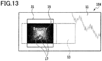
- Fig. 11 is a cross-sectional view showing a layer configuration of watermarked paper according to the fourth embodiment.
- Watermarked paper 104 of the present embodiment is provided with both of the diffraction structure part 15 of the second embodiment and the printed layer 16 of the third embodiment.
- the printed layer 16 may be drawn directly on the diffraction structure part 15 or a dimmer 12 instead of using a layer-forming material.
- the printed layer 16 In the configuration provided with the printed layer 16 and the diffraction structure part 15, in the case where the printed layer 16 is formed on top of the diffraction structure part 15 or between the diffraction structure part 15 and the dimmer 12, regardless of a condition of the dimmer 12, a pattern and the like of the printed layer 16 are visible.
- the printed layer 16 is preferably formed by materials which do not prevent light transmission.
- the printed layer 16 may be directly drawn on the dimmer 12 without a layer-forming material.
- Fig. 12 shows a state of observed watermarked paper of the present embodiment of which the dimmer is controlled to be transparent
- Fig. 13 shows a state of observed watermarked paper of the present embodiment of which the dimmer is controlled to be a mirror state.
- the watermarked paper 104 of the present embodiment when light is incident from a windowed part 31 where the dimmer 12 is exposed, the light is transmitted in the state where the dimmer 12 is controlled to be transparent, and hence, a watermark image printed on the printed layer 16 can be observed.
- the dimmer 12 is controlled to be a mirror state, even when light is incident from the windowed part 31 where the dimmer 12 is exposed, the light is blocked by the dimmer 12, and hence, a watermark image printed on the printed layer 16 cannot be observed.
- the dimmer by laminating, on the dimmer, the diffraction structure part with optical image information, with a change in voltage from the power supply to the dimmer, the dimmer serves as a reflection layer of the diffraction structure part and optical image information previously recorded on the diffraction structure part or a watermark image previously printed on the printed layer is allowed to be viewed from an exposure part provided on the paper.
- watermarked paper having multiple tones can be prepared by a method different from a dark watermarking method, and has high strength and surface smoothness, and has a structure in which a mixed intermediate layer is exposed on a part of the paper and optical change appears in the exposed part, and further, allows arbitrary change of a watermark pattern or display of recorded optical image information even during observation from the same field of view.
- Watermarked paper described above is not limited to an application such as forgery-preventing paper which uses a watermark effect as a forgery prevention measure, and for example, can be utilized also in the fields of decoration, toys, learning materials and the like.
- watermarked paper 101 of the first embodiment was prepared, and an effect thereof was examined.
- a polyethylene terephthalate (PET) film having a thickness of 25 ⁇ m was used as an intermediate layer base material 21.
- PET polyethylene terephthalate
- a water-soluble mask ink comprising the following composition 1 was applied/dried to a part to serve as an electrode in the dimming mirror layer by a gravure printing method, to form a first mask printed layer having a film thickness of 5 ⁇ m, and subsequently palladium was formed by a sputtering method so as to have a film thickness of 100 nm with parts other than necessary parts covered with a mask, and thus, a catalytic layer in the dimmer 12 was laminated.
- tantalum oxide was formed by a sputtering method so as to have a film thickness of 100 nm with parts other than the dimmer 12 covered with a mask, and thus, an electrolyte layer in the dimmer 12 was laminated.
- tungsten oxide was formed by a sputtering method so as to have a film thickness of 100 nm with parts other than the dimmer 12 covered with a mask, and thus, an ion storage layer in the dimmer 12 was prepared.
- ITO indium oxide and tin oxide
- the first mask layer and the second mask layer were removed by water washing and a part of the catalytic layer and of the conductive film layer were respectively exposed, and thus, an electrode was created.
- An IC chip was connected to this electrode, and further, an ink for a printed antenna comprising the following composition 2 was applied/dried in a desired antenna shape by a screen printing method on the intermediate layer base material 21 so that an end of the antenna was connected to the IC chip, to form an antenna, and thus, the dimmer 12 and the power supply 13 were provided on the intermediate layer base material 21.
- an adhesive layer ink comprising the following composition 3 was applied/dried to the entire front and back surfaces of the intermediate layer base material 21 by a gravure printing method to laminate an adhesive layer 14 having a film thickness of 3 ⁇ m, and thus, an intermediate layer 20 was prepared.
- softwood pulp was beaten in water to obtain those having a raw material concentration of 1.5 %, and subsequently was mixed one time using a handmade paper machine, and the intermediate layer 20 was arranged on the mixed softwood pulp and further were mixed once again and were dehydrated, and were heated and dried, to prepare watermarked paper 101 having a thickness of approximate 120 ⁇ m shown in Fig. 1 .
- watermarked paper 102 of the second embodiment was prepared, and an effect thereof was examined.
- a polyethylene terephthalate (PET) film having a thickness of 25 ⁇ m was used as an intermediate layer base material 21.
- An ink comprising the following composition 4 was applied/dried over the entire surface or in a part of one surface of the intermediate layer base material 21 by a gravure printing method to provide a diffraction structure layer having a film thickness of 1.5 ⁇ m, and subsequently, embossing was performed to press, against the diffraction structure layer, a relief plate for expressing a previously prepared diffracted light pattern of an image as shown in Fig. 13 (see Fig. 13 ) while applying thermal pressure, and thus, a desired diffraction structure part 15 was formed on the diffraction structure layer.
- Acrylic resin 10.0 parts by weight Isocyanate curing agent 8.0 parts by weight Methyl ethyl ketone 82.0 parts by weight
- a dimmer 12 on the diffraction structure part 15 parts other than the dimmer 12 were covered with a mask, and an alloy of magnesium and nickel was applied by a sputtering method so as to have a film thickness of 100 nm, and thus, a dimming mirror layer in the dimmer 12 was laminated.
- a water-soluble mask ink comprising the following composition 5 was applied/dried to a part to serve as an electrode in the dimming mirror layer by a gravure printing method, to form a first mask printed layer having a film thickness of 5 ⁇ m, and subsequently, palladium was formed by a sputtering method so as to have a film thickness of 100 nm with parts other than necessary parts covered with a mask, and thus, a catalytic layer in the dimmer 12 was laminated.
- tantalum oxide was applied by a sputtering method so as to have a film thickness of 100 nm with parts other than the dimmer 12 covered with a mask, and thus, an electrolyte layer in the dimmer 12 was laminated.
- tungsten oxide was applied by a sputtering method so as to have a film thickness of 100 nm with parts other than the dimmer 12 covered with a mask, and thus, an ion storage layer in the dimmer 12 was prepared.
- ITO indium oxide and tin oxide
- the first mask layer and the second mask layer were removed by water washing and a part of the catalytic layer and of the conductive film layer were respectively exposed, and thus, an electrode was created.
- An IC chip was connected to the electrode, and further, an ink for a printed antenna comprising the following composition 6 was applied/dried in a desired antenna shape by a screen printing method on the intermediate layer base material 21 so that an end of the antenna was connected to the IC chip, to form an antenna, and thus, the dimmer 12 and the power supply 13 were provided on the intermediate layer base material 21.
- an adhesive layer ink comprising the following composition 7 was applied/dried to the entire front and back surfaces of the intermediate layer base material 21 by a gravure printing method to laminate an adhesive layer 14 having a film thickness of 3 ⁇ m, and thus, an intermediate layer 20 having the diffraction structure part 15 was prepared.
- softwood pulp was beaten in water to obtain a raw material concentration of 1.5 %, and subsequently was mixed one time using a handmade paper machine, and the intermediate layer 20 was arranged on the mixed softwood pulp. Then, mixing was performed by the use of a papermaking net provided with a closed part to form a windowed part in a desired shape, and dehydration was performed and heating and drying was performed, to prepare the watermarked paper 102 having a thickness of 120 ⁇ m in which the diffraction structure part 15 could be seen from the windowed part 31.
- watermarked paper of the present invention changes a watermark pattern by power supply to a dimmer, and allows, when a diffraction structure is observed from a windowed part 31 provided on the paper, to control generation of diffracted light by power supply to the dimmer 12, and can change arbitrarily display of optical image information 17 recorded on the diffraction structure even during observation from the same field of view.
Landscapes
- Physics & Mathematics (AREA)
- General Physics & Mathematics (AREA)
- Optics & Photonics (AREA)
- Nonlinear Science (AREA)
- Paper (AREA)
- Credit Cards Or The Like (AREA)
- Printing Methods (AREA)
- Diffracting Gratings Or Hologram Optical Elements (AREA)
- Electrochromic Elements, Electrophoresis, Or Variable Reflection Or Absorption Elements (AREA)
Claims (5)
- Papier filigrané (100) obtenu en mélangeant, dans une couche de papier (11), une couche intermédiaire (20) avec une épaisseur de 6 à 300 µm qui présente un variateur (12) dont une quantité de transmission de lumière change selon un état de tension, dans lequel le papier filigrané comprend une alimentation électrique (13) pour fournir de l'électricité au variateur dans la couche intermédiaire ou sur une surface de papier,
caractérisé en ce qu'une image filigrane est changée en commutant le variateur entre un état transparent et un état miroir en commandant une tension par de l'électricité fournie depuis l'alimentation électrique, en ce que le papier filigrané comprend une partie fenêtrée (31) où une partie de la couche intermédiaire est exposée, et en ce que le papier filigrané comprend en outre une partie de structure de diffraction (15) sur laquelle des informations d'image optique qui servent d'image filigrane sont enregistrées, la partie de structure de diffraction étant stratifiée sur le variateur sur le côté de la partie fenêtrée. - Papier filigrané selon la revendication 1, caractérisé en ce que le variateur est formé dans un motif correspondant à l'image filigrane.
- Papier filigrané selon la revendication 1 ou 2, caractérisé en ce qu'un motif du variateur et des informations d'image optique de la partie de structure de diffraction ont une position correspondante.
- Papier filigrané selon l'une quelconque des revendications 1 à 3, caractérisé en ce qu'un motif du variateur et des informations d'image optique de la partie de structure de diffraction et la partie fenêtrée ont une position correspondante.
- Papier filigrané selon l'une quelconque des revendications 1 à 4, caractérisé en ce que le papier filigrané comprend en outre une couche imprimée présentant une image filigrane, la couche imprimée étant fournie sur le variateur sur le côté opposé à la partie fenêtrée.
Applications Claiming Priority (2)
| Application Number | Priority Date | Filing Date | Title |
|---|---|---|---|
| JP2015120500A JP6458658B2 (ja) | 2015-06-15 | 2015-06-15 | 透かし用紙 |
| PCT/JP2016/002902 WO2016203769A1 (fr) | 2015-06-15 | 2016-06-15 | Papier filigrané |
Publications (3)
| Publication Number | Publication Date |
|---|---|
| EP3308971A1 EP3308971A1 (fr) | 2018-04-18 |
| EP3308971A4 EP3308971A4 (fr) | 2019-02-27 |
| EP3308971B1 true EP3308971B1 (fr) | 2020-06-24 |
Family
ID=57545405
Family Applications (1)
| Application Number | Title | Priority Date | Filing Date |
|---|---|---|---|
| EP16811244.9A Active EP3308971B1 (fr) | 2015-06-15 | 2016-06-15 | Papier filigrané |
Country Status (5)
| Country | Link |
|---|---|
| US (1) | US10737525B2 (fr) |
| EP (1) | EP3308971B1 (fr) |
| JP (1) | JP6458658B2 (fr) |
| CN (1) | CN107709032B (fr) |
| WO (1) | WO2016203769A1 (fr) |
Families Citing this family (1)
| Publication number | Priority date | Publication date | Assignee | Title |
|---|---|---|---|---|
| CN114126888A (zh) * | 2019-07-15 | 2022-03-01 | 日本烟草国际股份有限公司 | 高光泽银色水印 |
Family Cites Families (30)
| Publication number | Priority date | Publication date | Assignee | Title |
|---|---|---|---|---|
| US4472627A (en) * | 1982-09-30 | 1984-09-18 | The United States Of America As Represented By The Secretary Of The Treasury | Authenticating and anti-counterfeiting device for currency |
| JPH0712153B2 (ja) | 1988-07-30 | 1995-02-08 | 日本電気株式会社 | Fm受信機 |
| JPH04149585A (ja) | 1990-10-12 | 1992-05-22 | Dainippon Printing Co Ltd | ステッカー |
| FR2707781B1 (fr) * | 1993-07-16 | 1995-09-01 | Idmatic Sa | Carte souple équipée d'un dispositif de contrôle de validité. |
| JP2002067470A (ja) | 2000-08-28 | 2002-03-05 | Nihon Unisys Supply Ltd | 透かし入用紙とその製造方法。 |
| JP4062430B2 (ja) * | 2002-09-11 | 2008-03-19 | 富士ゼロックス株式会社 | 電子メディア |
| JP4391287B2 (ja) | 2004-03-26 | 2009-12-24 | 大日本印刷株式会社 | 有価証券用紙 |
| DE102004045211B4 (de) * | 2004-09-17 | 2015-07-09 | Ovd Kinegram Ag | Sicherheitsdokument mit elektrisch gesteuertem Anzeigenelement |
| DE102004059798A1 (de) * | 2004-12-10 | 2006-06-29 | Ovd Kinegram Ag | Optisch variables Element mit elektrisch aktiver Schicht |
| US8330932B2 (en) * | 2004-12-10 | 2012-12-11 | Industrial Technology Research Institute | Bistable watermark |
| DE102006031422A1 (de) * | 2006-07-05 | 2008-01-10 | Bundesdruckerei Gmbh | Wert- oder Sicherheitsdokument mit einer Anzeigevorrichtung |
| EP1936603A1 (fr) * | 2006-12-19 | 2008-06-25 | European Central Bank | Procédé de production de cladribine |
| DE102007015934B4 (de) * | 2007-04-02 | 2021-04-01 | Bundesdruckerei Gmbh | Dokument mit einem Sicherheitsmerkmal, Lesegerät und Verfahren zum Lesen eines Sicherheitsmerkmals |
| EP1988514A1 (fr) * | 2007-05-04 | 2008-11-05 | Acreo AB | Circuit de document de sécurité |
| JP5136978B2 (ja) * | 2007-06-18 | 2013-02-06 | 独立行政法人産業技術総合研究所 | バッファ層を有する全固体型反射調光エレクトロクロミック素子及びそれを用いた調光部材 |
| DE102008012419A1 (de) * | 2007-10-31 | 2009-05-07 | Bundesdruckerei Gmbh | Polymerschichtverbund für ein Sicherheits- und/oder Wertdokument, Verfahren zu dessen Herstellung sowie Sicherheits- und/oder Wertdokument |
| FR2944229B1 (fr) * | 2009-04-10 | 2011-05-13 | Arjowiggins Security | Document a volets comportant une structure munie d'un filigrane ou pseudo-filigrane et procede associe |
| KR101243922B1 (ko) * | 2010-05-07 | 2013-03-14 | 삼성디스플레이 주식회사 | 디스플레이 장치 및 이의 제조 방법 |
| EP2576234B1 (fr) * | 2010-06-04 | 2015-08-26 | Polyvalor, Limited Partnership | Dispositifs de sécurité métamériques employant une matière active |
| US9708773B2 (en) * | 2011-02-23 | 2017-07-18 | Crane & Co., Inc. | Security sheet or document having one or more enhanced watermarks |
| JP5647047B2 (ja) * | 2011-03-18 | 2014-12-24 | 日本発條株式会社 | 識別媒体 |
| DE102011107421A1 (de) * | 2011-07-07 | 2013-01-10 | Leonhard Kurz Stiftung & Co. Kg | Mehrschichtiger Folienkörper |
| EP2757413A4 (fr) * | 2011-09-16 | 2015-05-27 | Nat Inst Of Advanced Ind Scien | Élément réfléchissant électrochromique de gradation dans lequel est insérée une couche électrolytique conductrice d'ions hydrogène non aqueuse, et élément de gradation utilisant ledit élément réfléchissant électrochromique de gradation |
| DE102011117129A1 (de) * | 2011-10-28 | 2013-05-02 | Leonhard Kurz Stiftung & Co. Kg | Anzeigeeinrichtung |
| JP5906680B2 (ja) * | 2011-11-11 | 2016-04-20 | 凸版印刷株式会社 | 偽造防止用紙 |
| JP2013186183A (ja) * | 2012-03-06 | 2013-09-19 | Toppan Tdk Label Co Ltd | エレクトロクロミック材料を用いたセキュリティーラベル |
| JP6003332B2 (ja) * | 2012-07-23 | 2016-10-05 | 株式会社リコー | エレクトロクロミック装置及びその製造方法 |
| WO2014017656A1 (fr) * | 2012-07-23 | 2014-01-30 | Ricoh Company, Ltd. | Dispositif électrochromique et procédé de fabrication d'un dispositif électrochromique |
| JP6064761B2 (ja) | 2012-11-02 | 2017-01-25 | 株式会社リコー | エレクトロクロミック装置及びその製造方法 |
| JP6658547B2 (ja) * | 2015-01-20 | 2020-03-04 | 凸版印刷株式会社 | 回折構造と調光素子とを備えた表示媒体 |
-
2015
- 2015-06-15 JP JP2015120500A patent/JP6458658B2/ja active Active
-
2016
- 2016-06-15 CN CN201680035128.9A patent/CN107709032B/zh not_active Expired - Fee Related
- 2016-06-15 EP EP16811244.9A patent/EP3308971B1/fr active Active
- 2016-06-15 WO PCT/JP2016/002902 patent/WO2016203769A1/fr active Application Filing
-
2017
- 2017-11-28 US US15/823,845 patent/US10737525B2/en active Active
Non-Patent Citations (1)
| Title |
|---|
| None * |
Also Published As
| Publication number | Publication date |
|---|---|
| CN107709032B (zh) | 2019-08-06 |
| EP3308971A1 (fr) | 2018-04-18 |
| US10737525B2 (en) | 2020-08-11 |
| JP2017001354A (ja) | 2017-01-05 |
| WO2016203769A1 (fr) | 2016-12-22 |
| CN107709032A (zh) | 2018-02-16 |
| EP3308971A4 (fr) | 2019-02-27 |
| US20180086131A1 (en) | 2018-03-29 |
| JP6458658B2 (ja) | 2019-01-30 |
Similar Documents
| Publication | Publication Date | Title |
|---|---|---|
| US8056820B2 (en) | Security structure, particularly for a security document and/or a valuable document | |
| CN102666124B (zh) | 显示体及带有显示体的物品 | |
| CN1325280C (zh) | 一种基片制造方法以及由该方法制得的产品 | |
| CN102956147B (zh) | 防伪膜及其制作方法 | |
| GB2464496A (en) | Printed security features | |
| CN105263719B (zh) | 制造具有阴文字的防伪元件的方法 | |
| CA2703342A1 (fr) | Ameliorations apportees a des elements de securite | |
| US11623466B2 (en) | Display medium provided with diffraction structure and light control element | |
| EP3308971B1 (fr) | Papier filigrané | |
| JP5906680B2 (ja) | 偽造防止用紙 | |
| CN101670725B (zh) | 夹芯层含磁性膜的防伪元件、含该元件的纸制品及其各自的制作方法 | |
| JP6213465B2 (ja) | 偽造防止用紙 | |
| CN213844569U (zh) | 一种新型防伪标签 | |
| JP6705323B2 (ja) | 表示媒体、該表示媒体を貼付した物品及び表示方法 | |
| JP5891611B2 (ja) | 偽造防止用紙 | |
| JP2005066872A (ja) | 装飾シートおよびその製造方法 | |
| JP6120025B2 (ja) | 偽造防止用紙 | |
| CN112634742A (zh) | 一种新型防伪标签及其制作方法 | |
| JP2008049643A (ja) | 偽造防止磁気テープ転写シートおよびカード | |
| JPH0858274A (ja) | 情報担持シート | |
| JP2018096004A (ja) | 偽造防止用紙 |
Legal Events
| Date | Code | Title | Description |
|---|---|---|---|
| STAA | Information on the status of an ep patent application or granted ep patent |
Free format text: STATUS: THE INTERNATIONAL PUBLICATION HAS BEEN MADE |
|
| PUAI | Public reference made under article 153(3) epc to a published international application that has entered the european phase |
Free format text: ORIGINAL CODE: 0009012 |
|
| STAA | Information on the status of an ep patent application or granted ep patent |
Free format text: STATUS: REQUEST FOR EXAMINATION WAS MADE |
|
| 17P | Request for examination filed |
Effective date: 20171205 |
|
| AK | Designated contracting states |
Kind code of ref document: A1 Designated state(s): AL AT BE BG CH CY CZ DE DK EE ES FI FR GB GR HR HU IE IS IT LI LT LU LV MC MK MT NL NO PL PT RO RS SE SI SK SM TR |
|
| AX | Request for extension of the european patent |
Extension state: BA ME |
|
| DAV | Request for validation of the european patent (deleted) | ||
| DAX | Request for extension of the european patent (deleted) | ||
| A4 | Supplementary search report drawn up and despatched |
Effective date: 20190128 |
|
| RIC1 | Information provided on ipc code assigned before grant |
Ipc: B42D 25/333 20140101AFI20190122BHEP Ipc: G02B 5/18 20060101ALI20190122BHEP Ipc: D21H 21/40 20060101ALI20190122BHEP Ipc: B42D 25/351 20140101ALI20190122BHEP Ipc: B42D 25/36 20140101ALI20190122BHEP Ipc: G02F 1/15 20190101ALI20190122BHEP Ipc: B41M 3/14 20060101ALI20190122BHEP Ipc: B42D 25/328 20140101ALI20190122BHEP |
|
| GRAP | Despatch of communication of intention to grant a patent |
Free format text: ORIGINAL CODE: EPIDOSNIGR1 |
|
| STAA | Information on the status of an ep patent application or granted ep patent |
Free format text: STATUS: GRANT OF PATENT IS INTENDED |
|
| INTG | Intention to grant announced |
Effective date: 20200213 |
|
| RIN1 | Information on inventor provided before grant (corrected) |
Inventor name: IDE, HIDETAKA |
|
| GRAS | Grant fee paid |
Free format text: ORIGINAL CODE: EPIDOSNIGR3 |
|
| GRAA | (expected) grant |
Free format text: ORIGINAL CODE: 0009210 |
|
| STAA | Information on the status of an ep patent application or granted ep patent |
Free format text: STATUS: THE PATENT HAS BEEN GRANTED |
|
| AK | Designated contracting states |
Kind code of ref document: B1 Designated state(s): AL AT BE BG CH CY CZ DE DK EE ES FI FR GB GR HR HU IE IS IT LI LT LU LV MC MK MT NL NO PL PT RO RS SE SI SK SM TR |
|
| REG | Reference to a national code |
Ref country code: GB Ref legal event code: FG4D |
|
| REG | Reference to a national code |
Ref country code: CH Ref legal event code: EP |
|
| REG | Reference to a national code |
Ref country code: AT Ref legal event code: REF Ref document number: 1283510 Country of ref document: AT Kind code of ref document: T Effective date: 20200715 |
|
| REG | Reference to a national code |
Ref country code: DE Ref legal event code: R096 Ref document number: 602016038830 Country of ref document: DE |
|
| REG | Reference to a national code |
Ref country code: IE Ref legal event code: FG4D |
|
| PG25 | Lapsed in a contracting state [announced via postgrant information from national office to epo] |
Ref country code: GR Free format text: LAPSE BECAUSE OF FAILURE TO SUBMIT A TRANSLATION OF THE DESCRIPTION OR TO PAY THE FEE WITHIN THE PRESCRIBED TIME-LIMIT Effective date: 20200925 Ref country code: FI Free format text: LAPSE BECAUSE OF FAILURE TO SUBMIT A TRANSLATION OF THE DESCRIPTION OR TO PAY THE FEE WITHIN THE PRESCRIBED TIME-LIMIT Effective date: 20200624 Ref country code: NO Free format text: LAPSE BECAUSE OF FAILURE TO SUBMIT A TRANSLATION OF THE DESCRIPTION OR TO PAY THE FEE WITHIN THE PRESCRIBED TIME-LIMIT Effective date: 20200924 Ref country code: LT Free format text: LAPSE BECAUSE OF FAILURE TO SUBMIT A TRANSLATION OF THE DESCRIPTION OR TO PAY THE FEE WITHIN THE PRESCRIBED TIME-LIMIT Effective date: 20200624 Ref country code: SE Free format text: LAPSE BECAUSE OF FAILURE TO SUBMIT A TRANSLATION OF THE DESCRIPTION OR TO PAY THE FEE WITHIN THE PRESCRIBED TIME-LIMIT Effective date: 20200624 |
|
| REG | Reference to a national code |
Ref country code: LT Ref legal event code: MG4D |
|
| PG25 | Lapsed in a contracting state [announced via postgrant information from national office to epo] |
Ref country code: RS Free format text: LAPSE BECAUSE OF FAILURE TO SUBMIT A TRANSLATION OF THE DESCRIPTION OR TO PAY THE FEE WITHIN THE PRESCRIBED TIME-LIMIT Effective date: 20200624 Ref country code: HR Free format text: LAPSE BECAUSE OF FAILURE TO SUBMIT A TRANSLATION OF THE DESCRIPTION OR TO PAY THE FEE WITHIN THE PRESCRIBED TIME-LIMIT Effective date: 20200624 Ref country code: LV Free format text: LAPSE BECAUSE OF FAILURE TO SUBMIT A TRANSLATION OF THE DESCRIPTION OR TO PAY THE FEE WITHIN THE PRESCRIBED TIME-LIMIT Effective date: 20200624 Ref country code: BG Free format text: LAPSE BECAUSE OF FAILURE TO SUBMIT A TRANSLATION OF THE DESCRIPTION OR TO PAY THE FEE WITHIN THE PRESCRIBED TIME-LIMIT Effective date: 20200924 |
|
| REG | Reference to a national code |
Ref country code: NL Ref legal event code: MP Effective date: 20200624 |
|
| REG | Reference to a national code |
Ref country code: AT Ref legal event code: MK05 Ref document number: 1283510 Country of ref document: AT Kind code of ref document: T Effective date: 20200624 |
|
| PG25 | Lapsed in a contracting state [announced via postgrant information from national office to epo] |
Ref country code: AL Free format text: LAPSE BECAUSE OF FAILURE TO SUBMIT A TRANSLATION OF THE DESCRIPTION OR TO PAY THE FEE WITHIN THE PRESCRIBED TIME-LIMIT Effective date: 20200624 Ref country code: NL Free format text: LAPSE BECAUSE OF FAILURE TO SUBMIT A TRANSLATION OF THE DESCRIPTION OR TO PAY THE FEE WITHIN THE PRESCRIBED TIME-LIMIT Effective date: 20200624 |
|
| PG25 | Lapsed in a contracting state [announced via postgrant information from national office to epo] |
Ref country code: PT Free format text: LAPSE BECAUSE OF FAILURE TO SUBMIT A TRANSLATION OF THE DESCRIPTION OR TO PAY THE FEE WITHIN THE PRESCRIBED TIME-LIMIT Effective date: 20201026 Ref country code: CZ Free format text: LAPSE BECAUSE OF FAILURE TO SUBMIT A TRANSLATION OF THE DESCRIPTION OR TO PAY THE FEE WITHIN THE PRESCRIBED TIME-LIMIT Effective date: 20200624 Ref country code: RO Free format text: LAPSE BECAUSE OF FAILURE TO SUBMIT A TRANSLATION OF THE DESCRIPTION OR TO PAY THE FEE WITHIN THE PRESCRIBED TIME-LIMIT Effective date: 20200624 Ref country code: ES Free format text: LAPSE BECAUSE OF FAILURE TO SUBMIT A TRANSLATION OF THE DESCRIPTION OR TO PAY THE FEE WITHIN THE PRESCRIBED TIME-LIMIT Effective date: 20200624 Ref country code: EE Free format text: LAPSE BECAUSE OF FAILURE TO SUBMIT A TRANSLATION OF THE DESCRIPTION OR TO PAY THE FEE WITHIN THE PRESCRIBED TIME-LIMIT Effective date: 20200624 Ref country code: SM Free format text: LAPSE BECAUSE OF FAILURE TO SUBMIT A TRANSLATION OF THE DESCRIPTION OR TO PAY THE FEE WITHIN THE PRESCRIBED TIME-LIMIT Effective date: 20200624 Ref country code: AT Free format text: LAPSE BECAUSE OF FAILURE TO SUBMIT A TRANSLATION OF THE DESCRIPTION OR TO PAY THE FEE WITHIN THE PRESCRIBED TIME-LIMIT Effective date: 20200624 Ref country code: IT Free format text: LAPSE BECAUSE OF FAILURE TO SUBMIT A TRANSLATION OF THE DESCRIPTION OR TO PAY THE FEE WITHIN THE PRESCRIBED TIME-LIMIT Effective date: 20200624 |
|
| PG25 | Lapsed in a contracting state [announced via postgrant information from national office to epo] |
Ref country code: SK Free format text: LAPSE BECAUSE OF FAILURE TO SUBMIT A TRANSLATION OF THE DESCRIPTION OR TO PAY THE FEE WITHIN THE PRESCRIBED TIME-LIMIT Effective date: 20200624 Ref country code: PL Free format text: LAPSE BECAUSE OF FAILURE TO SUBMIT A TRANSLATION OF THE DESCRIPTION OR TO PAY THE FEE WITHIN THE PRESCRIBED TIME-LIMIT Effective date: 20200624 Ref country code: IS Free format text: LAPSE BECAUSE OF FAILURE TO SUBMIT A TRANSLATION OF THE DESCRIPTION OR TO PAY THE FEE WITHIN THE PRESCRIBED TIME-LIMIT Effective date: 20201024 |
|
| REG | Reference to a national code |
Ref country code: DE Ref legal event code: R097 Ref document number: 602016038830 Country of ref document: DE |
|
| PG25 | Lapsed in a contracting state [announced via postgrant information from national office to epo] |
Ref country code: DK Free format text: LAPSE BECAUSE OF FAILURE TO SUBMIT A TRANSLATION OF THE DESCRIPTION OR TO PAY THE FEE WITHIN THE PRESCRIBED TIME-LIMIT Effective date: 20200624 |
|
| PLBE | No opposition filed within time limit |
Free format text: ORIGINAL CODE: 0009261 |
|
| STAA | Information on the status of an ep patent application or granted ep patent |
Free format text: STATUS: NO OPPOSITION FILED WITHIN TIME LIMIT |
|
| 26N | No opposition filed |
Effective date: 20210325 |
|
| PG25 | Lapsed in a contracting state [announced via postgrant information from national office to epo] |
Ref country code: SI Free format text: LAPSE BECAUSE OF FAILURE TO SUBMIT A TRANSLATION OF THE DESCRIPTION OR TO PAY THE FEE WITHIN THE PRESCRIBED TIME-LIMIT Effective date: 20200624 |
|
| REG | Reference to a national code |
Ref country code: DE Ref legal event code: R119 Ref document number: 602016038830 Country of ref document: DE |
|
| PG25 | Lapsed in a contracting state [announced via postgrant information from national office to epo] |
Ref country code: MC Free format text: LAPSE BECAUSE OF FAILURE TO SUBMIT A TRANSLATION OF THE DESCRIPTION OR TO PAY THE FEE WITHIN THE PRESCRIBED TIME-LIMIT Effective date: 20200624 |
|
| REG | Reference to a national code |
Ref country code: CH Ref legal event code: PL |
|
| GBPC | Gb: european patent ceased through non-payment of renewal fee |
Effective date: 20210615 |
|
| REG | Reference to a national code |
Ref country code: BE Ref legal event code: MM Effective date: 20210630 |
|
| PG25 | Lapsed in a contracting state [announced via postgrant information from national office to epo] |
Ref country code: LU Free format text: LAPSE BECAUSE OF NON-PAYMENT OF DUE FEES Effective date: 20210615 |
|
| PG25 | Lapsed in a contracting state [announced via postgrant information from national office to epo] |
Ref country code: LI Free format text: LAPSE BECAUSE OF NON-PAYMENT OF DUE FEES Effective date: 20210630 Ref country code: IE Free format text: LAPSE BECAUSE OF NON-PAYMENT OF DUE FEES Effective date: 20210615 Ref country code: GB Free format text: LAPSE BECAUSE OF NON-PAYMENT OF DUE FEES Effective date: 20210615 Ref country code: DE Free format text: LAPSE BECAUSE OF NON-PAYMENT OF DUE FEES Effective date: 20220101 Ref country code: CH Free format text: LAPSE BECAUSE OF NON-PAYMENT OF DUE FEES Effective date: 20210630 |
|
| PG25 | Lapsed in a contracting state [announced via postgrant information from national office to epo] |
Ref country code: FR Free format text: LAPSE BECAUSE OF NON-PAYMENT OF DUE FEES Effective date: 20210630 |
|
| PG25 | Lapsed in a contracting state [announced via postgrant information from national office to epo] |
Ref country code: BE Free format text: LAPSE BECAUSE OF NON-PAYMENT OF DUE FEES Effective date: 20210630 |
|
| PG25 | Lapsed in a contracting state [announced via postgrant information from national office to epo] |
Ref country code: CY Free format text: LAPSE BECAUSE OF FAILURE TO SUBMIT A TRANSLATION OF THE DESCRIPTION OR TO PAY THE FEE WITHIN THE PRESCRIBED TIME-LIMIT Effective date: 20200624 |
|
| PG25 | Lapsed in a contracting state [announced via postgrant information from national office to epo] |
Ref country code: HU Free format text: LAPSE BECAUSE OF FAILURE TO SUBMIT A TRANSLATION OF THE DESCRIPTION OR TO PAY THE FEE WITHIN THE PRESCRIBED TIME-LIMIT; INVALID AB INITIO Effective date: 20160615 |
|
| PG25 | Lapsed in a contracting state [announced via postgrant information from national office to epo] |
Ref country code: MK Free format text: LAPSE BECAUSE OF FAILURE TO SUBMIT A TRANSLATION OF THE DESCRIPTION OR TO PAY THE FEE WITHIN THE PRESCRIBED TIME-LIMIT Effective date: 20200624 |
|
| PG25 | Lapsed in a contracting state [announced via postgrant information from national office to epo] |
Ref country code: MT Free format text: LAPSE BECAUSE OF FAILURE TO SUBMIT A TRANSLATION OF THE DESCRIPTION OR TO PAY THE FEE WITHIN THE PRESCRIBED TIME-LIMIT Effective date: 20200624 |