EP3308405B1 - Bauteil zum detektieren elektromagnetischer strahlung - Google Patents
Bauteil zum detektieren elektromagnetischer strahlung Download PDFInfo
- Publication number
- EP3308405B1 EP3308405B1 EP16729834.8A EP16729834A EP3308405B1 EP 3308405 B1 EP3308405 B1 EP 3308405B1 EP 16729834 A EP16729834 A EP 16729834A EP 3308405 B1 EP3308405 B1 EP 3308405B1
- Authority
- EP
- European Patent Office
- Prior art keywords
- functional layer
- elements
- substrate
- wavelength range
- electromagnetic radiation
- Prior art date
- Legal status (The legal status is an assumption and is not a legal conclusion. Google has not performed a legal analysis and makes no representation as to the accuracy of the status listed.)
- Active
Links
Images

Classifications
-
- H—ELECTRICITY
- H10—SEMICONDUCTOR DEVICES; ELECTRIC SOLID-STATE DEVICES NOT OTHERWISE PROVIDED FOR
- H10F—INORGANIC SEMICONDUCTOR DEVICES SENSITIVE TO INFRARED RADIATION, LIGHT, ELECTROMAGNETIC RADIATION OF SHORTER WAVELENGTH OR CORPUSCULAR RADIATION
- H10F39/00—Integrated devices, or assemblies of multiple devices, comprising at least one element covered by group H10F30/00, e.g. radiation detectors comprising photodiode arrays
- H10F39/10—Integrated devices
- H10F39/103—Integrated devices the at least one element covered by H10F30/00 having potential barriers, e.g. integrated devices comprising photodiodes or phototransistors
-
- H—ELECTRICITY
- H10—SEMICONDUCTOR DEVICES; ELECTRIC SOLID-STATE DEVICES NOT OTHERWISE PROVIDED FOR
- H10F—INORGANIC SEMICONDUCTOR DEVICES SENSITIVE TO INFRARED RADIATION, LIGHT, ELECTROMAGNETIC RADIATION OF SHORTER WAVELENGTH OR CORPUSCULAR RADIATION
- H10F30/00—Individual radiation-sensitive semiconductor devices in which radiation controls the flow of current through the devices, e.g. photodetectors
- H10F30/20—Individual radiation-sensitive semiconductor devices in which radiation controls the flow of current through the devices, e.g. photodetectors the devices having potential barriers, e.g. phototransistors
- H10F30/21—Individual radiation-sensitive semiconductor devices in which radiation controls the flow of current through the devices, e.g. photodetectors the devices having potential barriers, e.g. phototransistors the devices being sensitive to infrared, visible or ultraviolet radiation
- H10F30/288—Individual radiation-sensitive semiconductor devices in which radiation controls the flow of current through the devices, e.g. photodetectors the devices having potential barriers, e.g. phototransistors the devices being sensitive to infrared, visible or ultraviolet radiation the devices being sensitive to multiple wavelengths, e.g. multi-spectrum radiation detection devices
-
- H—ELECTRICITY
- H10—SEMICONDUCTOR DEVICES; ELECTRIC SOLID-STATE DEVICES NOT OTHERWISE PROVIDED FOR
- H10F—INORGANIC SEMICONDUCTOR DEVICES SENSITIVE TO INFRARED RADIATION, LIGHT, ELECTROMAGNETIC RADIATION OF SHORTER WAVELENGTH OR CORPUSCULAR RADIATION
- H10F55/00—Radiation-sensitive semiconductor devices covered by groups H10F10/00, H10F19/00 or H10F30/00 being structurally associated with electric light sources and electrically or optically coupled thereto
- H10F55/18—Radiation-sensitive semiconductor devices covered by groups H10F10/00, H10F19/00 or H10F30/00 being structurally associated with electric light sources and electrically or optically coupled thereto wherein the radiation-sensitive semiconductor devices and the electric light source share a common body having dual-functionality of light emission and light detection
-
- H—ELECTRICITY
- H10—SEMICONDUCTOR DEVICES; ELECTRIC SOLID-STATE DEVICES NOT OTHERWISE PROVIDED FOR
- H10K—ORGANIC ELECTRIC SOLID-STATE DEVICES
- H10K19/00—Integrated devices, or assemblies of multiple devices, comprising at least one organic element specially adapted for rectifying, amplifying, oscillating or switching, covered by group H10K10/00
- H10K19/201—Integrated devices having a three-dimensional layout, e.g. 3D ICs
-
- H—ELECTRICITY
- H10—SEMICONDUCTOR DEVICES; ELECTRIC SOLID-STATE DEVICES NOT OTHERWISE PROVIDED FOR
- H10K—ORGANIC ELECTRIC SOLID-STATE DEVICES
- H10K39/00—Integrated devices, or assemblies of multiple devices, comprising at least one organic radiation-sensitive element covered by group H10K30/00
- H10K39/30—Devices controlled by radiation
- H10K39/32—Organic image sensors
-
- H—ELECTRICITY
- H10—SEMICONDUCTOR DEVICES; ELECTRIC SOLID-STATE DEVICES NOT OTHERWISE PROVIDED FOR
- H10K—ORGANIC ELECTRIC SOLID-STATE DEVICES
- H10K65/00—Integrated devices, or assemblies of multiple devices, comprising at least one organic light-emitting element and at least one organic radiation-sensitive element, e.g. organic opto-couplers
-
- H—ELECTRICITY
- H10—SEMICONDUCTOR DEVICES; ELECTRIC SOLID-STATE DEVICES NOT OTHERWISE PROVIDED FOR
- H10K—ORGANIC ELECTRIC SOLID-STATE DEVICES
- H10K19/00—Integrated devices, or assemblies of multiple devices, comprising at least one organic element specially adapted for rectifying, amplifying, oscillating or switching, covered by group H10K10/00
- H10K19/20—Integrated devices, or assemblies of multiple devices, comprising at least one organic element specially adapted for rectifying, amplifying, oscillating or switching, covered by group H10K10/00 comprising components having an active region that includes an inorganic semiconductor
Definitions
- the invention relates to components for detecting electromagnetic radiation, with which both multispectral sensors and sensor-emitter systems can be realized.
- a multispectral sensor is to be understood as a component with which electromagnetic radiation from at least two different wavelength ranges can be detected
- a sensor-emitter system is to be understood as a component which comprises both at least one element detecting electromagnetic radiation and at least one element emitting electromagnetic radiation.
- a bolometer on a substrate with an emitter on the other side of the substrate is made of US 2007/0029482 A1 known.
- Bidirectional displays are known on which several light-generating image elements and several light-capturing elements are arranged in the form of an array.
- the light-generating image elements as a whole can function, for example, as the display surface of a display and the light-capturing elements as a whole can function, for example, as the sensor of a camera.
- WO 2012/163312 A1 also describes various control variants of the elements that solve the problem of direct crosstalk from light-generating image elements to adjacent light-detecting elements by controlling the light-generating image elements and adjacent light-detecting elements one after the other. As a result, light-generating image elements and adjacent light-detecting elements are only active one after the other.
- the WO 2012/163312 A1 revealed control variants to their limits.
- the inactivity of the light-generating image elements during an exposure time of light-capturing elements which requires a certain length for good signal quality, can lead to perceptible image disturbances, or at least to a visible loss of brightness.
- the sensitivity of the detector elements cannot be increased arbitrarily, since display applications require ever higher resolutions, whereby the chip area used should be kept as small as possible for cost reasons, so that the space for detector elements or circuitry measures to increase their sensitivity is severely limited.
- a component according to the invention should be able to be used to create multispectral sensors by means of which electromagnetic radiation of different wavelength ranges can be detected, as well as sensor-emitter systems that have a high degree of filling with regard to the function of detecting as well as with regard to the function of emitting electromagnetic radiation.
- the elements that implement the functions of detecting or emitting electromagnetic radiation are not arranged next to one another within a layer, but a separate functional layer is formed for all elements that implement one and the same function, with the individual functional layers being arranged one above the other. In this way, Elements that realize a function can achieve an increased degree of filling compared to the state of the art.
- a component according to the invention therefore comprises a first functional layer within which a large number of first elements are formed, by means of which electromagnetic radiation from a first wavelength range can be detected, the first functional layer being deposited on one side of a substrate.
- the first functional layer preferably has a large number of first elements that detect electromagnetic radiation, which are preferably arranged in a grid pattern over the first functional layer. All components that can be formed within a functional layer and with which electromagnetic radiation can be detected are suitable as a detector element.
- a detector element can be designed as a photodiode or as a photo field effect transistor.
- a component according to the invention also comprises a second functional layer within which a large number of second elements are formed, by means of which second elements electromagnetic radiation from a second wavelength range can be emitted.
- the second functional layer is deposited on the side of the substrate that is opposite the first functional layer.
- the second functional layer has a plurality of second elements, all of which perform an electromagnetic radiation-emitting function.
- the plurality of second elements is also preferably arranged in a grid pattern over the surface of the second functional layer.
- the second wavelength range can be selected, for example, from the range of infrared radiation, the range of radiation that can be detected by the human eye, the range of X-rays or the range of ultraviolet radiation.
- a functional layer that includes elements that detect electromagnetic radiation is also referred to as a detector layer or, in short, as a detector and a Functional layer which comprises elements that emit electrical radiation, referred to as emitter layer or, in short, emitter.
- the first wavelength range preferably differs from the second wavelength range.
- the first functional layer and the second functional layer preferably consist of an organic material. Process steps for forming elements (within an organic layer) with which electromagnetic radiation can be detected or electromagnetic radiation can be emitted are known.
- the organic material from which the first functional layer and/or the second functional layer consists also comprises nanoparticles which are embedded within the organic material. Such nanoparticles can be formed, for example, as so-called quantum nanoparticles (also referred to as quantum nanodots or QND for short).
- Plastics or glasses are suitable as substrate materials.
- a semiconductor substrate for example a silicon substrate
- a circuit structure consisting of active components (such as a CMOS structure) and at least one connection level consisting of a plurality of conductor tracks are formed within the substrate.
- the semiconductor substrate also has at least one via, by means of which a detector element or an emitter element from a functional layer is electrically connected to a conductor track of the connection level within the substrate.
- a component 10 not according to the invention is shown schematically in a section.
- the component 10 comprises a substrate 11, on one side of which a first functional layer 12 and on the other side of which a second functional layer 13 are deposited. Both functional layers 12 and 13 consist of an organic material.
- a plurality of Fig. 1 first photodiodes (not shown) are formed, which are arranged in a grid pattern over the surface of the functional layer 12 and by means of which electromagnetic radiation 14 from a first wavelength range, such as the ultraviolet wavelength range, can be detected.
- the functional layer 12 is thus designed as a detector for UV radiation.
- Fig. 1 second photodiodes (also not shown) are formed, which are arranged in a grid pattern over the surface of the functional layer 13 and by means of which electromagnetic radiation 15 from a second wavelength range, such as the infrared wavelength range, can be detected.
- the functional layer 13 is thus also designed as a detector, but this time for IR radiation.
- the substrate 11 and the functional layer 12 are also transparent to IR radiation.
- the component 10 can thus detect both UV radiation and IR radiation that radiates onto the component 10 from the side of the functional layer 12.
- the substrate 11 consists of a silicon material which already comprises a CMOS structure and thus a logic circuit which is used for controlling the photodiodes formed within the functional layers 11 and 12.
- a Fig. 1 A wiring level (also not shown) is formed, with the conductor tracks of which the contacts of the photodiodes formed in the functional layers are connected.
- the photodiodes formed in the functional layer 12 are directly contacted with the adjacent conductor tracks of the wiring level, while the photodiodes formed within the functional layer 13 are connected by means of so-called through-silicon vias (hereinafter referred to as "TSVs") are contacted with the conductor tracks of the wiring level through the substrate 11.
- TSVs through-silicon vias
- Fig. 2 shows an alternative multispectral sensor 20, which initially includes all features of the multispectral sensor 10 from Fig. 1
- a plurality of Fig. 2 Third photodiodes (not shown) are formed, which are arranged in a grid pattern over the surface of the substrate 11 and by means of which electromagnetic radiation 26 from the wavelength range that can be detected by a human eye can be detected.
- the substrate 11 is thus also formed as a detector for electromagnetic radiation from a third wavelength range. Process steps for forming photodiodes within a semiconductor substrate are also known.
- the third photodiodes are also connected within the substrate 11 by means of the wiring level that is formed on one side of the substrate 11, as already described. Fig. 1 described.
- electromagnetic rays of three different wavelength ranges can thus be detected, which act on the component 20 from the side on which the functional layer 12 is deposited.
- the functional layer 12 is transparent to the electromagnetic radiation that is detected with the third photodiodes within the substrate 11.
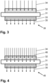
- Fig. 3 another alternative component 30 not according to the invention is shown schematically, which is designed as a sensor-emitter system.
- the component 30 comprises a substrate 31 made of a silicon-based semiconductor material within which a CMOS structure, a wiring level and TSVs vias are already formed, as is the case with substrate 11 made of Fig. 1
- a first functional layer 32 made of an organic material is deposited, within which a plurality of Fig. 3 first photodiodes (not shown) are formed, which are arranged in a grid pattern over the surface of the functional layer 32 and by means of which electromagnetic radiation 34 from a first wavelength range, such as the infrared wavelength range, can be detected.
- the functional layer 32 is thus formed as a detector for IR radiation.
- the photodiodes within the functional layer 32 are contacted with the conductor tracks of the wiring level of the substrate 31 and are controlled by means of the CMOS circuit formed within the substrate 31.
- the sensor-emitter system 30 can be used, for example, as an image converter in night vision devices by evaluating the data of the IR radiation image detected by the sensor 32 with the CMOS circuit in the substrate 31 and reproducing a radiation image on the emitter 33 that can be perceived by the human eye.
Landscapes
- Light Receiving Elements (AREA)
- Photometry And Measurement Of Optical Pulse Characteristics (AREA)
- Electroluminescent Light Sources (AREA)
- Chemical & Material Sciences (AREA)
- Composite Materials (AREA)
- Solid State Image Pick-Up Elements (AREA)
Description
- Die Erfindung betrifft Bauteile zum Detektieren elektromagnetischer Strahlung, mit denen sowohl multispektrale Sensoren als auch Sensor-Emitter-Systeme realisiert werden können. Unter einem multispektralen Sensor soll ein Bauteil verstanden werden, mit welchem elektromagnetische Strahlung aus mindestens zwei unterschiedlichen Wellenlängenbereichen detektiert werden kann und unter einem Sensor-Emitter-System soll ein Bauteil verstanden werden, welches sowohl mindestens ein elektromagnetische Strahlung detektierendes Element als auch mindestens ein elektromagnetische Strahlung emittierendes Element umfasst.
- Ein Bolometer auf einem Substrat mit einem Emitter auf der anderen Seite des Substrats ist aus
US 2007/0029482 A1 bekannt. - Ein Bauteil, mittels dessen elektromagnetische Strahlung verschiedener Wellenlängenbereiche detektiert werden kann, ist aus
US 2003/209651 A1 bekannt. Nachteilig wirkt sich hierbei aus, dass ein solches Bauteil nicht als Sensor-Emitter-System verwendet werden kann. -
DE 10 2006 030 541 A1 undUS 2015/108508 A1 beschreiben Sensor-Emitter-Systeme, bei denen sich elektromagnetische Strahlung emittierende Elemente und elektromagnetische Strahlung detektierende Elemente gemeinsam nebeneinander auf einem Chip befinden. Dabei können beide Elementarten in einer Matrix auf dem Chip angeordnet sein. Nachteilig wirkt sich hierbei aus, dass die unmittelbar angrenzende Anordnung von elektromagnetische Strahlung emittierenden Elementen und elektromagnetische Strahlung detektierenden Elementen zum Überkoppeln führt. - Aus
WO 2012/163312 A1 und BERND RICHTER ET AL: "Bidirectional OLED microdisplay: Combining display and image sensor functionality into a monolithic CMOS chip", SOID-STATE CIRCUITS CONFERENCE DIGEST OF TECHNICAL PAPERS (ISSCC), 2011, IEEE, Seiten 314 - 316, sind bidirektionale Displays bekannt, auf denen mehrere lichterzeugende Bildelemente und mehrere lichterfassende Elemente in Form eines Arrays angeordnet sind. Dabei können die lichterzeugenden Bildelemente in ihrer Gesamtheit beispielsweise als Anzeigefläche eines Displays und die lichterfassenden Elemente in ihrer Gesamtheit beispielsweise als Sensor einer Kamera fungieren.WO 2012/163312 A1 beschreibt ferner verschiedene Ansteuervarianten der Elemente, die das Problem des direkten Übersprechens von lichterzeugenden Bildelementen auf angrenzende lichterfassende Elemente lösen sollen, indem die lichterzeugenden Bildelemente und angrenzende lichterfassende Elemente nacheinander angesteuert werden. Dadurch sind lichterzeugende Bildelemente und angrenzende lichterfassende Elemente nur abwechselnd nacheinander aktiv wirksam. - Fungieren die lichterzeugenden Bildelemente einer bidirektionalen Vorrichtung als Display, stoßen die in
WO 2012/163312 A1 offenbarten Ansteuervarianten an ihre Grenzen. - Insbesondere die Inaktivität der lichterzeugenden Bildelemente während einer Belichtungszeit von lichterfassenden Elementen, die für eine gute Signalqualität eine bestimmte Länge erfordert, kann zu wahrnehmbaren Bildstörungen, mindestens aber zu einem sichtbaren Helligkeitsverlust führen. Die Sensitivität der Detektorelemente wiederum kann nicht beliebig gesteigert werden, da bei Displayanwendungen immer höhere Auflösungen gefordert werden, wobei die verwendete Chipfläche aus Kostengründen möglichst gering bleiben soll, so dass damit der Platz für Detektorelemente bzw. schaltungstechnische Maßnahmen zum Steigern derer Sensitivität stark eingeschränkt sind.
- Ein weiteres Problem bekannter Sensor-Emitter-Systeme, bei denen Strahlung detektierende Elemente und Strahlung emittierende Elemente nebeneinander angeordnet sind, stellt der geringe Füllgrad bezüglich der beiden Funktionen dar. D.h., sowohl für das Detektieren als auch für das Emittieren von Strahlung steht nur ein relativ geringer Oberflächenbereich eines solchen Sensor-Emitter-Systems zur Verfügung, weil die anderen Oberflächenbereiche durch Elemente der jeweils anderen Funktion bzw. durch Flächenbereiche, die für das Verdrahten der Elemente benötigt werden, bedeckt sind.
- Der Erfindung liegt daher das technische Problem zugrunde, ein Bauteil zu schaffen, mit dem die Nachteile aus dem Stand der Technik überwunden werden können. Insbesondere sollen sich mit einem erfindungsgemäßen Bauteil multispektrale Sensoren realisieren lassen, mittels denen elektromagnetische Strahlung unterschiedlicher Wellenlängenbereiche detektierbar ist als auch Sensor-Emitter-Systeme, die einen hohen Füllgrad bezüglich der Funktion des Detektierens als auch bezüglich der Funktion des Emittierens elektromagnetischer Strahlung aufweisen.
- Die Lösung des technischen Problems ergibt sich durch die Gegenstände mit den Merkmalen des Patentanspruchs 1. Weitere vorteilhafte Ausgestaltungen der Erfindung ergeben sich aus den abhängigen Ansprüchen.
- Bei einem erfindungsgemäßen Bauteil sind die Elemente, die Funktionen des Detektierens oder des Emittierens elektromagnetischer Strahlung realisieren nicht nebeneinander innerhalb einer Schicht angeordnet, sondern für alle Elemente die ein und dieselbe Funktion realisieren, ist jeweils eine separate Funktionsschicht ausgebildet, wobei die einzelnen Funktionsschichten übereinander liegend angeordnet sind. Auf diese Weise kann für die Elemente, die eine Funktion realisieren, ein gegenüber dem Stand der Technik erhöhter Füllgrad erzielt werden.
- Ein erfindungsgemäßes Bauteil umfasst daher eine erste Funktionsschicht, innerhalb der eine Vielzahl erster Elemente ausgebildet ist, mittels dem elektromagnetische Strahlung aus einem ersten Wellenlängenbereich detektierbar ist, wobei die erste Funktionsschicht auf einer Seite eines Substrates abgeschieden ist. Bevorzugt weist die erste Funktionsschicht eine Vielzahl von elektromagnetische Strahlung detektierenden ersten Elementen auf, die vorzugsweise rasterförmig über die erste Funktionsschicht verteilt angeordnet sind. Als Detektorelement sind alle Bauelemente geeignet, die innerhalb einer Funktionsschicht ausgebildet werden können und mit denen elektromagnetische Strahlung detektierbar ist. So kann ein Detektorelement beispielsweise als Fotodiode oder als Foto-Feldeffekttransistor ausgebildet sein. Mit diesen Detektorelementen der ersten Funktionsschicht kann beispielsweise elektromagnetische Strahlung aus dem Bereich der Infrarotstrahlung, dem Bereich der Strahlung, der mit einem menschlichen Auge erfassbar ist, dem Bereich der Röntgenstrahlung oder aus dem Bereich der Ultraviolettstrahlung erfasst werden. Ein erfindungsgemäßes Bauteil umfasst außerdem eine zweite Funktionsschicht, innerhalb der eine Vielzahl zweiter Elemente ausgebildet ist, mittels der zweiter Elemente elektromagnetische Strahlung aus einem zweiten Wellenlängenbereich emittierbar. Dabei ist die zweite Funktionsschicht auf der Seite des Substrates abgeschieden, die der ersten Funktionsschicht gegenüber liegt. Die zweite Funktionsschicht weist eine Vielzahl von zweiten Elementen auf, die alle eine elektronmagnetische Strahlung emittierende Funktion ausführen. Auch die Vielzahl zweiter Elemente ist vorzugsweise rasterförmig über die Fläche der zweiten Funktionsschicht verteilt angeordnet. Der zweite Wellenlängenbereich kann beispielsweise aus dem Bereich der Infrarotstrahlung, dem Bereich der Strahlung, der mit einem menschlichen Auge erfassbar ist, dem Bereich der Röntgenstrahlung oder aus dem Bereich der Ultraviolettstrahlung ausgewählt sein.
- Eine Funktionsschicht, die elektromagnetische Strahlung detektierende Elemente umfasst, wird nachfolgend auch als Detektor-Schicht oder verkürzt als Detektor bezeichnet und eine Funktionsschicht, welche elektrische Strahlung emittierende Elemente umfasst, als Emitter-Schicht oder verkürzt als Emitter.
- Wenn die erste Funktionsschicht und die zweite Funktionsschicht jeweils als Detektor ausgebildet sind, unterscheidet sich der erste Wellenlängenbereich vorzugsweise vom zweiten Wellenlängenbereich. Mittels eines solchen erfindungsgemäßen Bauteils kann dann elektromagnetische Strahlung, die von der Seite der ersten Funktionsschicht auf das Bauteil einfällt, in zwei verschiedenen Wellenlängenbereichen detektiert werden.
- Bevorzugt bestehen die erste Funktionsschicht und die zweite Funktionsschicht aus einem organischen Material. Verfahrensschritte zum Ausbilden von Elementen (innerhalb einer organischen Schicht) mit denen elektromagnetische Strahlung detektiert oder elektromagnetische Strahlung emittiert werden kann, sind bekannt. Bei einer Ausführungsform umfasst das organische Material, aus welchem die erste Funktionsschicht und/oder die zweite Funktionsschicht besteht, auch noch Nanopartikel, welche innerhalb des organischen Materials eingelagert sind. Derartige Nanopartikel können beispielsweise als sogenannte Quantum-Nanopartikel (auch als Quantum-Nano-Dots oder verkürzt als QND bezeichnet) ausgebildet sein. Als Substratmaterial sind Kunststoffe oder Gläser geeignet. Bevorzugt wird jedoch als Substrat eines erfindungsgemäßen Bauteils ein Halbleitersubstrat (beispielsweise ein Siliziumsubstrat) verwendet.
- Bei einer Ausführungsform sind innerhalb des Substrats eine Schaltungsstruktur, bestehend aus aktiven Bauelementen (wie beispielsweise eine CMOS-Struktur) sowie mindestens eine Verbindungsebene, bestehend aus einer Vielzahl von Leiterbahnen, ausgebildet. Ebenfalls weist das Halbleitersubstrat mindestens eine Durchkontaktierung auf, mittels der ein Detektorelement oder ein Emitterelement aus einer Funktionsschicht mit einer Leiterbahn der Verbindungsebene innerhalb des Substrates elektrisch leitend verbunden ist.
- Die vorliegende Erfindung wird nachfolgend anhand von Ausführungsbeispielen näher erläutert. Die Fig. zeigen:
- Fig. 1
- eine schematische Schnittdarstellung des Aufbaus eines nicht erfindungsgemäßen Bauteils mit zwei Detektoren;
- Fig. 2
- eine schematische Schnittdarstellung des Aufbaus eines nicht erfindungsgemäßen Bauteils mit zwei Detektoren und einem als Detektor ausgebildeten Substrat;
- Fig. 3
- eine schematische Schnittdarstellung des Aufbaus eines nicht erfindungsgemäßen Bauteils mit einem Detektor und einem Emitter;
- Fig. 4
- eine schematische Schnittdarstellung des Aufbaus eines erfindungsgemäßen Bauteils mit einem Detektor und einem Emitter sowie einem als Detektor ausgebildetem Substrat.
- In
Fig. 1 ist ein nicht erfindungsgemäßes Bauteil 10 in einem Schnitt schematisch dargestellt. Das Bauteil 10 umfasst ein Substrat 11, auf dessen einen Seite eine erste Funktionsschicht 12 und auf dessen anderen Seite eine zweite Funktionsschicht 13 abgeschieden sind. Beide Funktionsschichten 12 und 13 bestehen aus einem organischen Material. Innerhalb der Funktionsschicht 12 ist eine Vielzahl von inFig. 1 nicht dargestellten ersten Fotodioden ausgebildet, die rasterförmig über die Fläche der Funktionsschicht 12 verteilt angeordnet sind und mittels denen elektromagnetische Strahlung 14 aus einem ersten Wellenlängenbereich, wie beispielsweise dem Ultraviolett-Wellenlängenbereich, detektierbar ist. Die Funktionsschicht 12 ist somit als Detektor für UV-Strahlung ausgebildet. - Innerhalb der Funktionsschicht 13 ist eine Vielzahl von in
Fig. 1 ebenfalls nicht dargestellten zweiten Fotodioden ausgebildet, die rasterförmig über die Fläche der Funktionsschicht 13 verteilt angeordnet sind und mittels denen elektromagnetische Strahlung 15 aus einem zweiten Wellenlängenbereich, wie beispielsweise dem Infrarot-Wellenlängenbereich, detektierbar ist. Die Funktionsschicht 13 ist somit ebenfalls als Detektor aber diesmal für IR-Strahlung ausgebildet. Das Substrat 11 und die Funktionsschicht 12 sind außerdem transparent gegenüber IR-Strahlung. Mit dem Bauteil 10 kann somit sowohl UV-Strahlung als auch IR-Strahlung detektiert werden, die von der Seite der Funktionsschicht 12 auf das Bauteil 10 einstrahlt. - Das Substrat 11 besteht aus einem Siliziummaterial, das bereits eine CMOS-Struktur und somit eine Logikschaltung umfasst, welche für das Ansteuern der innerhalb der Funktionsschichten 11 und 12 ausgebildeten Fotodioden verwendet wird. Auf der Seite des Substrates 11, die an die Funktionsschicht 12 angrenzt, ist eine in
Fig. 1 ebenso nicht dargestellte Verdrahtungsebene ausgebildet, mit deren Leiterbahnen die Kontakte der in den Funktionsschichten ausgebildeten Fotodioden verschaltet werden. Dabei sind die in der Funktionsschicht 12 ausgebildeten Fotodioden direkt mit den angrenzenden Leiterbahnen der Verdrahtungsebene kontaktiert, während die innerhalb der Funktionsschicht 13 ausgebildeten Fotodioden mittels sogenannter Through-Silicon-Vias (nachfolgend als "TSVs" bezeichnet) durch das Substrat 11 hindurch mit den Leiterbahnen der Verdrahtungsebene kontaktiert sind. Der Vollständigkeit halber sei erwähnt, dass Verfahrensschritte zum Ausbilden einer Schaltungsstruktur aus aktiven Bauelementen und einer Verdrahtungsebene innerhalb eines Substrates aus einem Halbleitermaterial sowie Verfahrensschritte zum Ausbilden von Kontaktierungen durch ein solches Substrat hindurch bekannt sind. - Das Verwenden der Verdrahtungsebene eines Substrates für das Verschalten von Fotodioden innerhalb übereinander angeordneter Funktionsschichten ermöglicht einen hohen Füllfaktor einer jeden Funktionsschicht mit elektromagnetische Strahlung detektierenden Elementen gegenüber bekannten optoelektronischen Bauteilen, bei denen die Verdrahtung innerhalb der Funktionsschicht selbst erfolgt. Mit dem Bauteil 10 wurde somit ein multispektraler Sensor mit einem gegenüber dem Stand der Technik erhöhten Auflösungsgrad realisiert.
-
Fig. 2 zeigt einen alternativen multispektralen Sensor 20, der zunächst alle Merkmale des multispektralen Sensors 10 ausFig. 1 aufweist. Zusätzlich sind jedoch beim multispektralen Sensor 20 innerhalb des Substrates 11 eine Vielzahl von inFig. 2 nicht dargestellten dritten Fotodioden ausgebildet, die rasterförmig über die Fläche des Substrates 11 verteilt angeordnet sind und mittels denen elektromagnetische Strahlung 26 aus dem Wellenlängenbereich, der mit einem menschlichen Auge erfasst werden kann, detektierbar ist. Das Substrat 11 ist somit auch noch als Detektor für elektromagnetische Strahlung aus einem dritten Wellenlängenbereich ausgebildet. Verfahrensschritte für das Ausbilden von Fotodioden innerhalb eines Halbleitersubstrates sind ebenfalls bekannt. Die Verschaltung der dritten Fotodioden innerhalb des Substrates 11 erfolgt ebenfalls mittels der Verdrahtungsebene, die an einer Seite des Substrates 11 ausgebildet ist, wie es bereits zuFig. 1 beschrieben wurde. Mit einem multispektralen Sensor 20 können somit elektromagnetische Strahlen dreier verschiedener Wellenlängenbereiche detektiert werden, die von der Seite das Bauteil 20 beaufschlagen, an welcher die Funktionsschicht 12 abgeschieden ist. Hierfür ist es zusätzlich noch erforderlich, dass die Funktionsschicht 12 transparent gegenüber der elektromagnetischen Strahlung ausgebildet ist, die mit den dritten Fotodioden innerhalb des Substrates 11 detektiert wird. - In
Fig. 3 ist ein weiteres alternatives nicht erfindungsgemäßes Bauteil 30 schematisch dargestellt, welches als Sensor-Emitter-System ausgebildet ist. Das Bauteil 30 umfasst ein Substrat 31 aus einem Halbleitermaterial auf Siliziumbasis, innerhalb dem bereits eine CMOS-Struktur, eine Verdrahtungsebene und TSVs-Durchkontaktierungen ausgebildet sind, so wie es zu Substrat 11 ausFig. 1 beschrieben wurde. Auf einer Seite des Substrates 31 ist eine erste Funktionsschicht 32 aus einem organischen Material abgeschieden, innerhalb der eine Vielzahl von inFig. 3 nicht dargestellten ersten Fotodioden ausgebildet sind, die rasterförmig über die Fläche der Funktionsschicht 32 verteilt angeordnet sind und mittels denen elektromagnetische Strahlung 34 aus einem ersten Wellenlängenbereich, wie beispielsweise dem Infrarot-Wellenlängenbereich detektierbar ist. Die Funktionsschicht 32 ist somit als Detektor für IR-Strahlung ausgebildet. Die Fotodioden innerhalb der Funktionsschicht 32 sind mit den Leiterbahnen der Verdrahtungsebene des Substrates 31 kontaktiert und werden mittels der innerhalb des Substrates 31 ausgebildeten CMOS-Schaltung angesteuert. - Auf der anderen Seite des Substrates 31 ist eine zweite Funktionsschicht 33 aus einem organischen Material abgeschieden. Innerhalb der Funktionsschicht 33 ist eine Vielzahl von in
Fig. 1 nicht dargestellter Leuchtdioden ausgebildet, die rasterförmig über die Fläche der Funktionsschicht 12 verteilt angeordnet sind und mittels denen elektromagnetische Strahlung 35 dem Wellenlängenbereich, der mit einem menschlichen Auge erfassbar ist, emittiert. Die Funktionsschicht 33 ist somit als Emitter ausgebildet. Mittels den im Substrat 31 ausgebildeten TSVs werden die Leuchtdioden der Funktionsschicht 33 mit den Leiterzügen der Verdrahtungsebene kontaktiert und über die CMOS-Schaltung im Substrat 31 angesteuert. Das Sensor-Emitter-System 30 kann beispielsweise als Bildwandler in Nachtsichtgeräten verwendet werden, indem die Daten des mit dem Sensor 32 detektierten IR-Strahlungsbildes mit der CMOS-Schaltung im Substrat 31 ausgewertet werden und auf dem Emitter 33 ein Strahlungsbild wiedergegeben wird, dass mit einem menschlichen Auge erfasst werden kann. - Ein alternatives Sensor-Emitter-System 40 ist in
Fig. 4 schematisch dargestellt, das zunächst alle Merkmale des Sensor-Emitter-Systems 30 ausFig. 3 aufweist. Zusätzlich ist jedoch beim Sensor-Emitter-System 40 innerhalb des Substrates 31 eine Vielzahl von inFig. 4 nicht dargestellten dritten Fotodioden ausgebildet, die rasterförmig über die Fläche des Substrates 31 verteilt angeordnet sind und mittels denen elektromagnetische Strahlung 46 aus dem Ultraviolett-Wellenlängenbereich detektierbar ist. Das Substrat 31 ist somit auch noch als Detektor für elektromagnetische Strahlung aus dem UV-Wellenlängenbereich ausgebildet. Das Verschalten der dritten Fotodioden innerhalb des Substrates 31 erfolgt mittels der Verdrahtungsebene, die an einer Seite des Substrates 31 ausgebildet ist. Mit einem erfindungsgemäßen Sensor-Emitter-System, gemäßFig. 4 , lassen sich somit Strahlungsbilder aus zwei unterschiedlichen Wellenlängenbereichen mittels der Detektoren 31 und 32 erfassen und können separat oder auch akkumuliert als Strahlungsbild in einem dritten Wellenlängenbereich mittels des Emitters 33 wiedergegeben werden. - Es sei angemerkt, dass die in den
Fig. 1 bis 4 genannten und den einzelnen Detektoren und Emittern zugeordneten Wellenlängenbereiche bezüglich elektromagnetischer Strahlung nur beispielhaft genannt wurden. Den einzelnen Detektoren und Emittern kann aber auch jeder andere beliebige Wellenlängenbereich elektromagnetischer Strahlung zugeordnet werden, der mit bekannten Sensoren detektiert bzw. mit bekannten Emittern emittiert werden kann.
Claims (6)
- Bauteil (40), umfassend eine erste Funktionsschicht (32), innerhalb der eine Vielzahl als Fotodiode oder Foto-Feldeffekttransistor fungierender erster Elemente ausgebildet ist, mittels der auf die Oberfläche der ersten Funktionsschicht (32) auftreffende elektromagnetische Strahlung (34) aus einem ersten Wellenlängenbereich detektierbar ist, wobei die erste Funktionsschicht (32) auf einer Seite eines aus einem Halbleitermaterial bestehenden und eine Schaltungsstruktur aus aktiven Bauelementen umfassenden Substrates (31) abgeschieden ist, wobei auf der Seite des Substrates (31), welche der ersten Funktionsschicht (32) gegenüberliegt, eine zweite Funktionsschicht (33) abgeschieden ist, innerhalb der eine Vielzahl zweiter Elemente ausgebildet ist, mittels der elektromagnetische Strahlung (35) aus einem zweiten Wellenlängenbereich emittierbar ist, wobei sich der erste Wellenlängenbereich vom zweiten Wellenlängenbereich unterscheidet, dadurch gekennzeichnet, dass innerhalb des Substrates (31) eine Vielzahl als Fotodiode ausgebildeter dritter Elemente ausgebildet ist, mittels der auf die Oberfläche der ersten Funktionsschicht (32) auftreffende elektromagnetische Strahlung (46) aus einem dritten Wellenlängenbereich detektierbar ist, wobei sich der dritte Wellenlängenbereich vom ersten und zweiten Wellenlängenbereich unterscheidet und die erste Funktionsschicht (32) transparent bezüglich elektromagnetischer Strahlung (46) aus dem dritten Wellenlängenbereich ist, so dass Strahlungsbilder aus dem ersten Wellenlängenbereich und dem dritten Wellenlängenbereich mittels der ersten Elemente und der dritten Elemente erfassbar sind und separat oder akkumuliert als Strahlungsbild im zweiten Wellenlängenbereich mittels der zweiten Elemente wiedergegeben werden können.
- Bauteil nach Anspruch 1, dadurch gekennzeichnet, dass das Substrat (31) mindestens eine Verdrahtungsebene umfasst.
- Bauteil nach einem der vorhergehenden Ansprüche, dadurch gekennzeichnet, dass das Substrat (31) mindestens eine Durchkontaktierung aufweist.
- Bauteil nach einem der vorhergehenden Ansprüche, dadurch gekennzeichnet, dass innerhalb der ersten Funktionsschicht (32), innerhalb der zweiten Funktionsschicht (33) und/oder innerhalb des Substrates (31) eine Vielzahl von jeweils zugehörigen ersten Elementen, zweiten Elementen bzw. dritten Elementen ausgebildet sind, die über die Fläche der jeweiligen Funktionsschicht (32; 33) bzw. über die Fläche des Substrates (31) verteilt rasterförmig angeordnet sind.
- Bauteil nach einem der vorhergehenden Ansprüche, dadurch gekennzeichnet, dass die erste Funktionsschicht (32) und/oder die zweite Funktionsschicht (33) ein organisches Material umfassen.
- Bauteil nach Anspruch 5, dadurch gekennzeichnet, dass die erste Funktionsschicht (32) und/oder die zweite Funktionsschicht (33) Nanopartikel umfasst.
Applications Claiming Priority (2)
| Application Number | Priority Date | Filing Date | Title |
|---|---|---|---|
| DE102015109044.9A DE102015109044B4 (de) | 2015-06-09 | 2015-06-09 | Bauteil zum Detektieren elektromagnetischer Strahlung |
| PCT/EP2016/062865 WO2016198382A1 (de) | 2015-06-09 | 2016-06-07 | Bauteil zum detektieren elektromagnetischer strahlung |
Publications (3)
| Publication Number | Publication Date |
|---|---|
| EP3308405A1 EP3308405A1 (de) | 2018-04-18 |
| EP3308405B1 true EP3308405B1 (de) | 2024-12-18 |
| EP3308405B8 EP3308405B8 (de) | 2025-01-22 |
Family
ID=56134321
Family Applications (1)
| Application Number | Title | Priority Date | Filing Date |
|---|---|---|---|
| EP16729834.8A Active EP3308405B8 (de) | 2015-06-09 | 2016-06-07 | Bauteil zum detektieren elektromagnetischer strahlung |
Country Status (5)
| Country | Link |
|---|---|
| US (1) | US10644070B2 (de) |
| EP (1) | EP3308405B8 (de) |
| CN (1) | CN107980175A (de) |
| DE (1) | DE102015109044B4 (de) |
| WO (1) | WO2016198382A1 (de) |
Families Citing this family (4)
| Publication number | Priority date | Publication date | Assignee | Title |
|---|---|---|---|---|
| US10115000B2 (en) | 2015-12-11 | 2018-10-30 | Synaptics Incorporated | Method and system for optical imaging using patterned illumination |
| DE102019102176B4 (de) | 2019-01-29 | 2022-11-24 | Senorics Gmbh | Hybrides multispektrales Bauelement |
| DE102019210315A1 (de) * | 2019-07-12 | 2021-01-14 | Audi Ag | Sichtbauteil mit funktionaler Beschichtung |
| CN112802862B (zh) * | 2020-12-31 | 2025-06-27 | 南京大学 | 基于复合介质栅双晶体管光敏探测器的光谱传感器 |
Citations (2)
| Publication number | Priority date | Publication date | Assignee | Title |
|---|---|---|---|---|
| US20070029482A1 (en) * | 2005-08-05 | 2007-02-08 | Philips Laou | Infrared imager |
| US20080179520A1 (en) * | 2007-01-30 | 2008-07-31 | Northrop Grumman Corporation | Direct-view focal plane array |
Family Cites Families (25)
| Publication number | Priority date | Publication date | Assignee | Title |
|---|---|---|---|---|
| JPS60130274A (ja) * | 1983-12-19 | 1985-07-11 | Toshiba Corp | 固体撮像装置 |
| DE3533146A1 (de) * | 1985-09-17 | 1987-03-26 | Siemens Ag | Farbsensorelement, farbempfindliche sensoranordnung mit derartigen farbsensorelementen, eine anwendung des elements oder der anordnung und ein verfahren zur herstellung eines halbleitermaterials fuer das farbsensorelement |
| JPS62281381A (ja) * | 1986-05-29 | 1987-12-07 | Mitsubishi Cable Ind Ltd | 光半導体素子 |
| DE3633181C2 (de) * | 1986-09-30 | 1998-12-10 | Siemens Ag | Reflexlichtschranke |
| US5604136A (en) * | 1995-05-26 | 1997-02-18 | National Science Council | Method of manufacturing light converter with amorphous-silicon pin heterojunction diode |
| DE19714054A1 (de) | 1997-04-05 | 1998-10-08 | Daimler Benz Ag | SiGe-Photodetektor mit hohem Wirkungsgrad |
| DE19807782A1 (de) * | 1998-02-18 | 1999-09-02 | Siemens Ag | Bauelement mit einem Lichtsender und einem Lichtempfänger |
| US7129466B2 (en) * | 2002-05-08 | 2006-10-31 | Canon Kabushiki Kaisha | Color image pickup device and color light-receiving device |
| US7381953B1 (en) * | 2003-07-25 | 2008-06-03 | Public Service Solutions, Inc. | Infrared imaging device |
| DE102006030541B4 (de) | 2006-06-23 | 2010-05-12 | Fraunhofer-Gesellschaft zur Förderung der angewandten Forschung e.V. | Optische Anordnung |
| US8686365B2 (en) * | 2008-07-28 | 2014-04-01 | Infrared Newco, Inc. | Imaging apparatus and methods |
| CN101533846B (zh) * | 2009-04-03 | 2011-06-08 | 中国科学院苏州纳米技术与纳米仿生研究所 | 用于辐射计量的光释光剂量元件及其制备方法 |
| JP2011065133A (ja) * | 2009-08-20 | 2011-03-31 | Toppan Printing Co Ltd | 液晶表示装置、ブラックマトリクス基板、及びカラーフィルタ基板 |
| US8399889B2 (en) * | 2009-11-09 | 2013-03-19 | Solarmer Energy, Inc. | Organic light emitting diode and organic solar cell stack |
| JP2011159858A (ja) * | 2010-02-02 | 2011-08-18 | Sony Corp | 固体撮像装置およびその製造方法、電子機器 |
| JP5554139B2 (ja) * | 2010-05-11 | 2014-07-23 | パナソニック株式会社 | 複合型撮像素子およびそれを備えた撮像装置 |
| JP5767403B2 (ja) | 2011-05-31 | 2015-08-19 | フラウンホーファー・ゲゼルシャフト・ツール・フェルデルング・デア・アンゲヴァンテン・フォルシュング・エー・ファウ | 双方向ディスプレイおよびその制御方法 |
| US8653618B2 (en) * | 2011-09-02 | 2014-02-18 | Hoon Kim | Unit pixel of color image sensor and photo detector thereof |
| US20130075607A1 (en) * | 2011-09-22 | 2013-03-28 | Manoj Bikumandla | Image sensors having stacked photodetector arrays |
| US9385169B2 (en) * | 2011-11-29 | 2016-07-05 | Ignis Innovation Inc. | Multi-functional active matrix organic light-emitting diode display |
| US8749529B2 (en) * | 2012-03-01 | 2014-06-10 | Microsoft Corporation | Sensor-in-pixel display system with near infrared filter |
| US9356179B2 (en) * | 2012-06-22 | 2016-05-31 | Industrial Technology Research Institute | Display panel integrated with photoelectric device |
| JP6131955B2 (ja) * | 2012-08-09 | 2017-05-24 | ソニー株式会社 | 受発光素子及び受発光装置 |
| CN202758888U (zh) * | 2012-08-22 | 2013-02-27 | 标准科技股份有限公司 | 传感器封装模块 |
| US9362327B2 (en) * | 2014-01-15 | 2016-06-07 | Samsung Electronics Co., Ltd. | Image sensor and electronic device including the same |
-
2015
- 2015-06-09 DE DE102015109044.9A patent/DE102015109044B4/de active Active
-
2016
- 2016-06-07 EP EP16729834.8A patent/EP3308405B8/de active Active
- 2016-06-07 WO PCT/EP2016/062865 patent/WO2016198382A1/de not_active Ceased
- 2016-06-07 US US15/579,326 patent/US10644070B2/en active Active
- 2016-06-07 CN CN201680033490.2A patent/CN107980175A/zh active Pending
Patent Citations (2)
| Publication number | Priority date | Publication date | Assignee | Title |
|---|---|---|---|---|
| US20070029482A1 (en) * | 2005-08-05 | 2007-02-08 | Philips Laou | Infrared imager |
| US20080179520A1 (en) * | 2007-01-30 | 2008-07-31 | Northrop Grumman Corporation | Direct-view focal plane array |
Also Published As
| Publication number | Publication date |
|---|---|
| EP3308405A1 (de) | 2018-04-18 |
| EP3308405B8 (de) | 2025-01-22 |
| DE102015109044B4 (de) | 2020-10-08 |
| US20180182811A1 (en) | 2018-06-28 |
| DE102015109044A1 (de) | 2016-12-15 |
| WO2016198382A1 (de) | 2016-12-15 |
| CN107980175A (zh) | 2018-05-01 |
| US10644070B2 (en) | 2020-05-05 |
Similar Documents
| Publication | Publication Date | Title |
|---|---|---|
| DE102018126296B4 (de) | Berührungsanzeigevorrichtung und Berührungsanzeigetafel | |
| DE102016125952B4 (de) | Faltbare Anzeigevorrichtung | |
| EP2185994B1 (de) | Vorrichtung zur optischen navigation | |
| DE102017125366B4 (de) | Organische lichtemittierende anzeigevorrichtung | |
| DE69636240T2 (de) | Gerät zur Detektierung von Verdrahtungsfehlern auf einer Schaltplatine | |
| DE202019005984U1 (de) | Array-Substrat, Anzeigetafel und Anzeigevorrichtung | |
| DE102015109044B4 (de) | Bauteil zum Detektieren elektromagnetischer Strahlung | |
| DE112021003293T5 (de) | Bildanzeigevorrichtung und elektronische einrichtung | |
| DE102013113462A1 (de) | Organische leuchtdiodenvorrichtung und verfahren zum herstellen derselben | |
| DE102017222970B4 (de) | LIDAR Messsystem | |
| DE102018133407A1 (de) | Röntgenstrahlendetektor-vorrichtung | |
| DE102006030541A1 (de) | Optische Anordnung | |
| DE102005045895B3 (de) | CMOS Röntgenflachdetektor | |
| DE112021003272T5 (de) | Bildanzeigevorrichtung und elektronische einrichtung | |
| DE102017123290A1 (de) | Lichtemittierendes Bauteil, Anzeigevorrichtung und Verfahren zur Herstellung einer Anzeigevorrichtung | |
| DE102021108242A1 (de) | Bildsensor mit einer Anordung von optisch schaltbaren magnetischen Tunnelkontakten | |
| DE102009047202A1 (de) | Detektor | |
| WO2012149927A1 (de) | Bildsensor mit einstellbarer auflösung | |
| DE112021003265T5 (de) | Bildanzeigevorrichtung und elektronisches Gerät | |
| DE3317090A1 (de) | Fokusdetektor | |
| WO2018024549A1 (de) | Verfahren und vorrichtung zur vermessung einer vielzahl an halbleiterchips in einem waferverbund | |
| DE4422928A1 (de) | Zweidimensionaler Strahlungsdetektor | |
| EP3663806B1 (de) | Photonendetektor, verfahren zur herstellung eines photonendetektors und röntgengerät | |
| DE69132418T2 (de) | Informationsverarbeitungsanlage mit optischer Einstellmöglichkeit der Synapsengewichts-Matrix | |
| WO2019076900A1 (de) | Halbleiterbauteil |
Legal Events
| Date | Code | Title | Description |
|---|---|---|---|
| STAA | Information on the status of an ep patent application or granted ep patent |
Free format text: STATUS: THE INTERNATIONAL PUBLICATION HAS BEEN MADE |
|
| PUAI | Public reference made under article 153(3) epc to a published international application that has entered the european phase |
Free format text: ORIGINAL CODE: 0009012 |
|
| STAA | Information on the status of an ep patent application or granted ep patent |
Free format text: STATUS: REQUEST FOR EXAMINATION WAS MADE |
|
| 17P | Request for examination filed |
Effective date: 20171205 |
|
| AK | Designated contracting states |
Kind code of ref document: A1 Designated state(s): AL AT BE BG CH CY CZ DE DK EE ES FI FR GB GR HR HU IE IS IT LI LT LU LV MC MK MT NL NO PL PT RO RS SE SI SK SM TR |
|
| AX | Request for extension of the european patent |
Extension state: BA ME |
|
| DAV | Request for validation of the european patent (deleted) | ||
| DAX | Request for extension of the european patent (deleted) | ||
| STAA | Information on the status of an ep patent application or granted ep patent |
Free format text: STATUS: EXAMINATION IS IN PROGRESS |
|
| 17Q | First examination report despatched |
Effective date: 20201127 |
|
| RAP3 | Party data changed (applicant data changed or rights of an application transferred) |
Owner name: FRAUNHOFER-GESELLSCHAFT ZUR FOERDERUNG DER ANGEWANDTEN FORSCHUNG E.V. |
|
| GRAP | Despatch of communication of intention to grant a patent |
Free format text: ORIGINAL CODE: EPIDOSNIGR1 |
|
| STAA | Information on the status of an ep patent application or granted ep patent |
Free format text: STATUS: GRANT OF PATENT IS INTENDED |
|
| RIC1 | Information provided on ipc code assigned before grant |
Ipc: H01L 31/12 20060101ALI20240624BHEP Ipc: H01L 27/144 20060101ALI20240624BHEP Ipc: H01L 31/101 20060101AFI20240624BHEP |
|
| INTG | Intention to grant announced |
Effective date: 20240730 |
|
| GRAS | Grant fee paid |
Free format text: ORIGINAL CODE: EPIDOSNIGR3 |
|
| GRAA | (expected) grant |
Free format text: ORIGINAL CODE: 0009210 |
|
| STAA | Information on the status of an ep patent application or granted ep patent |
Free format text: STATUS: THE PATENT HAS BEEN GRANTED |
|
| AK | Designated contracting states |
Kind code of ref document: B1 Designated state(s): AL AT BE BG CH CY CZ DE DK EE ES FI FR GB GR HR HU IE IS IT LI LT LU LV MC MK MT NL NO PL PT RO RS SE SI SK SM TR |
|
| REG | Reference to a national code |
Ref country code: GB Ref legal event code: FG4D Free format text: NOT ENGLISH |
|
| REG | Reference to a national code |
Ref country code: CH Ref legal event code: PK Free format text: BERICHTIGUNG B8 Ref country code: CH Ref legal event code: EP |
|
| REG | Reference to a national code |
Ref country code: DE Ref legal event code: R096 Ref document number: 502016016837 Country of ref document: DE |
|
| RBV | Designated contracting states (corrected) |
Designated state(s): AL AT BE BG CH CY CZ DK EE ES FI FR GB GR HR HU IE IS IT LI LT LU LV MC MK MT NL NO PL PT RO RS SE SI SK SM TR |
|
| REG | Reference to a national code |
Ref country code: IE Ref legal event code: FG4D Free format text: LANGUAGE OF EP DOCUMENT: GERMAN Ref country code: DE Ref legal event code: R108 Ref document number: 502016016837 Country of ref document: DE |
|
| P01 | Opt-out of the competence of the unified patent court (upc) registered |
Free format text: CASE NUMBER: APP_66409/2024 Effective date: 20241216 |
|
| REG | Reference to a national code |
Ref country code: LT Ref legal event code: MG9D |
|
| PG25 | Lapsed in a contracting state [announced via postgrant information from national office to epo] |
Ref country code: HR Free format text: LAPSE BECAUSE OF FAILURE TO SUBMIT A TRANSLATION OF THE DESCRIPTION OR TO PAY THE FEE WITHIN THE PRESCRIBED TIME-LIMIT Effective date: 20241218 |
|
| PG25 | Lapsed in a contracting state [announced via postgrant information from national office to epo] |
Ref country code: FI Free format text: LAPSE BECAUSE OF FAILURE TO SUBMIT A TRANSLATION OF THE DESCRIPTION OR TO PAY THE FEE WITHIN THE PRESCRIBED TIME-LIMIT Effective date: 20241218 |
|
| PG25 | Lapsed in a contracting state [announced via postgrant information from national office to epo] |
Ref country code: BG Free format text: LAPSE BECAUSE OF FAILURE TO SUBMIT A TRANSLATION OF THE DESCRIPTION OR TO PAY THE FEE WITHIN THE PRESCRIBED TIME-LIMIT Effective date: 20241218 |
|
| PG25 | Lapsed in a contracting state [announced via postgrant information from national office to epo] |
Ref country code: NO Free format text: LAPSE BECAUSE OF FAILURE TO SUBMIT A TRANSLATION OF THE DESCRIPTION OR TO PAY THE FEE WITHIN THE PRESCRIBED TIME-LIMIT Effective date: 20250318 |
|
| REG | Reference to a national code |
Ref country code: NL Ref legal event code: MP Effective date: 20241218 |
|
| PG25 | Lapsed in a contracting state [announced via postgrant information from national office to epo] |
Ref country code: LV Free format text: LAPSE BECAUSE OF FAILURE TO SUBMIT A TRANSLATION OF THE DESCRIPTION OR TO PAY THE FEE WITHIN THE PRESCRIBED TIME-LIMIT Effective date: 20241218 Ref country code: GR Free format text: LAPSE BECAUSE OF FAILURE TO SUBMIT A TRANSLATION OF THE DESCRIPTION OR TO PAY THE FEE WITHIN THE PRESCRIBED TIME-LIMIT Effective date: 20250319 |
|
| PG25 | Lapsed in a contracting state [announced via postgrant information from national office to epo] |
Ref country code: RS Free format text: LAPSE BECAUSE OF FAILURE TO SUBMIT A TRANSLATION OF THE DESCRIPTION OR TO PAY THE FEE WITHIN THE PRESCRIBED TIME-LIMIT Effective date: 20250318 |
|
| PG25 | Lapsed in a contracting state [announced via postgrant information from national office to epo] |
Ref country code: NL Free format text: LAPSE BECAUSE OF FAILURE TO SUBMIT A TRANSLATION OF THE DESCRIPTION OR TO PAY THE FEE WITHIN THE PRESCRIBED TIME-LIMIT Effective date: 20241218 |
|
| PG25 | Lapsed in a contracting state [announced via postgrant information from national office to epo] |
Ref country code: SM Free format text: LAPSE BECAUSE OF FAILURE TO SUBMIT A TRANSLATION OF THE DESCRIPTION OR TO PAY THE FEE WITHIN THE PRESCRIBED TIME-LIMIT Effective date: 20241218 |
|
| PG25 | Lapsed in a contracting state [announced via postgrant information from national office to epo] |
Ref country code: PL Free format text: LAPSE BECAUSE OF FAILURE TO SUBMIT A TRANSLATION OF THE DESCRIPTION OR TO PAY THE FEE WITHIN THE PRESCRIBED TIME-LIMIT Effective date: 20241218 |
|
| PG25 | Lapsed in a contracting state [announced via postgrant information from national office to epo] |
Ref country code: ES Free format text: LAPSE BECAUSE OF FAILURE TO SUBMIT A TRANSLATION OF THE DESCRIPTION OR TO PAY THE FEE WITHIN THE PRESCRIBED TIME-LIMIT Effective date: 20241218 |
|
| PGFP | Annual fee paid to national office [announced via postgrant information from national office to epo] |
Ref country code: GB Payment date: 20250620 Year of fee payment: 10 |
|
| PG25 | Lapsed in a contracting state [announced via postgrant information from national office to epo] |
Ref country code: IS Free format text: LAPSE BECAUSE OF FAILURE TO SUBMIT A TRANSLATION OF THE DESCRIPTION OR TO PAY THE FEE WITHIN THE PRESCRIBED TIME-LIMIT Effective date: 20250418 |
|
| PG25 | Lapsed in a contracting state [announced via postgrant information from national office to epo] |
Ref country code: PT Free format text: LAPSE BECAUSE OF FAILURE TO SUBMIT A TRANSLATION OF THE DESCRIPTION OR TO PAY THE FEE WITHIN THE PRESCRIBED TIME-LIMIT Effective date: 20250421 |
|
| PGFP | Annual fee paid to national office [announced via postgrant information from national office to epo] |
Ref country code: FR Payment date: 20250618 Year of fee payment: 10 |
|
| PG25 | Lapsed in a contracting state [announced via postgrant information from national office to epo] |
Ref country code: RO Free format text: LAPSE BECAUSE OF FAILURE TO SUBMIT A TRANSLATION OF THE DESCRIPTION OR TO PAY THE FEE WITHIN THE PRESCRIBED TIME-LIMIT Effective date: 20241218 |
|
| PG25 | Lapsed in a contracting state [announced via postgrant information from national office to epo] |
Ref country code: SK Free format text: LAPSE BECAUSE OF FAILURE TO SUBMIT A TRANSLATION OF THE DESCRIPTION OR TO PAY THE FEE WITHIN THE PRESCRIBED TIME-LIMIT Effective date: 20241218 |
|
| PG25 | Lapsed in a contracting state [announced via postgrant information from national office to epo] |
Ref country code: CZ Free format text: LAPSE BECAUSE OF FAILURE TO SUBMIT A TRANSLATION OF THE DESCRIPTION OR TO PAY THE FEE WITHIN THE PRESCRIBED TIME-LIMIT Effective date: 20241218 |
|
| PG25 | Lapsed in a contracting state [announced via postgrant information from national office to epo] |
Ref country code: IT Free format text: LAPSE BECAUSE OF FAILURE TO SUBMIT A TRANSLATION OF THE DESCRIPTION OR TO PAY THE FEE WITHIN THE PRESCRIBED TIME-LIMIT Effective date: 20241218 |
|
| PG25 | Lapsed in a contracting state [announced via postgrant information from national office to epo] |
Ref country code: SE Free format text: LAPSE BECAUSE OF FAILURE TO SUBMIT A TRANSLATION OF THE DESCRIPTION OR TO PAY THE FEE WITHIN THE PRESCRIBED TIME-LIMIT Effective date: 20241218 |
|
| PG25 | Lapsed in a contracting state [announced via postgrant information from national office to epo] |
Ref country code: DK Free format text: LAPSE BECAUSE OF FAILURE TO SUBMIT A TRANSLATION OF THE DESCRIPTION OR TO PAY THE FEE WITHIN THE PRESCRIBED TIME-LIMIT Effective date: 20241218 |
|
| PLBE | No opposition filed within time limit |
Free format text: ORIGINAL CODE: 0009261 |
|
| STAA | Information on the status of an ep patent application or granted ep patent |
Free format text: STATUS: NO OPPOSITION FILED WITHIN TIME LIMIT |
|
| REG | Reference to a national code |
Ref country code: CH Ref legal event code: L10 Free format text: ST27 STATUS EVENT CODE: U-0-0-L10-L00 (AS PROVIDED BY THE NATIONAL OFFICE) Effective date: 20251029 |
|
| 26N | No opposition filed |
Effective date: 20250919 |
|
| REG | Reference to a national code |
Ref country code: CH Ref legal event code: H13 Free format text: ST27 STATUS EVENT CODE: U-0-0-H10-H13 (AS PROVIDED BY THE NATIONAL OFFICE) Effective date: 20260127 |
|
| PG25 | Lapsed in a contracting state [announced via postgrant information from national office to epo] |
Ref country code: MC Free format text: LAPSE BECAUSE OF FAILURE TO SUBMIT A TRANSLATION OF THE DESCRIPTION OR TO PAY THE FEE WITHIN THE PRESCRIBED TIME-LIMIT Effective date: 20241218 |
|
| PG25 | Lapsed in a contracting state [announced via postgrant information from national office to epo] |
Ref country code: LU Free format text: LAPSE BECAUSE OF NON-PAYMENT OF DUE FEES Effective date: 20250607 |
|
| REG | Reference to a national code |
Ref country code: BE Ref legal event code: MM Effective date: 20250630 |
|
| PG25 | Lapsed in a contracting state [announced via postgrant information from national office to epo] |
Ref country code: IE Free format text: LAPSE BECAUSE OF NON-PAYMENT OF DUE FEES Effective date: 20250607 |
|
| PG25 | Lapsed in a contracting state [announced via postgrant information from national office to epo] |
Ref country code: BE Free format text: LAPSE BECAUSE OF NON-PAYMENT OF DUE FEES Effective date: 20250630 |
|
| PG25 | Lapsed in a contracting state [announced via postgrant information from national office to epo] |
Ref country code: CH Free format text: LAPSE BECAUSE OF NON-PAYMENT OF DUE FEES Effective date: 20250630 |