EP3306670B1 - Structure de dispositif semi-conducteur ayant une paroi latérale non plane et méthode de fabrication utilisant un diélectrique doté - Google Patents
Structure de dispositif semi-conducteur ayant une paroi latérale non plane et méthode de fabrication utilisant un diélectrique doté Download PDFInfo
- Publication number
- EP3306670B1 EP3306670B1 EP17181954.3A EP17181954A EP3306670B1 EP 3306670 B1 EP3306670 B1 EP 3306670B1 EP 17181954 A EP17181954 A EP 17181954A EP 3306670 B1 EP3306670 B1 EP 3306670B1
- Authority
- EP
- European Patent Office
- Prior art keywords
- layer
- semiconductor
- dielectric material
- upper portion
- side wall
- Prior art date
- Legal status (The legal status is an assumption and is not a legal conclusion. Google has not performed a legal analysis and makes no representation as to the accuracy of the status listed.)
- Active
Links
- 239000004065 semiconductor Substances 0.000 title claims description 100
- 238000004519 manufacturing process Methods 0.000 title description 3
- 239000002019 doping agent Substances 0.000 claims description 47
- 239000000463 material Substances 0.000 claims description 47
- 239000003989 dielectric material Substances 0.000 claims description 42
- 238000000034 method Methods 0.000 claims description 25
- 229910052785 arsenic Inorganic materials 0.000 claims description 15
- RQNWIZPPADIBDY-UHFFFAOYSA-N arsenic atom Chemical compound [As] RQNWIZPPADIBDY-UHFFFAOYSA-N 0.000 claims description 15
- 238000005530 etching Methods 0.000 claims description 13
- 230000015572 biosynthetic process Effects 0.000 claims description 12
- 238000011065 in-situ storage Methods 0.000 claims description 10
- 230000008021 deposition Effects 0.000 claims description 9
- VYPSYNLAJGMNEJ-UHFFFAOYSA-N Silicium dioxide Chemical compound O=[Si]=O VYPSYNLAJGMNEJ-UHFFFAOYSA-N 0.000 claims description 7
- 229910052814 silicon oxide Inorganic materials 0.000 claims description 5
- FVBUAEGBCNSCDD-UHFFFAOYSA-N silicide(4-) Chemical group [Si-4] FVBUAEGBCNSCDD-UHFFFAOYSA-N 0.000 description 16
- 230000008569 process Effects 0.000 description 15
- 125000006850 spacer group Chemical group 0.000 description 14
- 150000002500 ions Chemical class 0.000 description 10
- 238000000151 deposition Methods 0.000 description 9
- 239000000758 substrate Substances 0.000 description 9
- 239000011800 void material Substances 0.000 description 8
- 238000002955 isolation Methods 0.000 description 5
- 229910052751 metal Inorganic materials 0.000 description 5
- 239000002184 metal Substances 0.000 description 5
- 229910021420 polycrystalline silicon Inorganic materials 0.000 description 5
- 229920005591 polysilicon Polymers 0.000 description 5
- 229910052581 Si3N4 Inorganic materials 0.000 description 4
- XUIMIQQOPSSXEZ-UHFFFAOYSA-N Silicon Chemical compound [Si] XUIMIQQOPSSXEZ-UHFFFAOYSA-N 0.000 description 4
- 150000004767 nitrides Chemical class 0.000 description 4
- 238000000059 patterning Methods 0.000 description 4
- 229910052710 silicon Inorganic materials 0.000 description 4
- 239000010703 silicon Substances 0.000 description 4
- HQVNEWCFYHHQES-UHFFFAOYSA-N silicon nitride Chemical compound N12[Si]34N5[Si]62N3[Si]51N64 HQVNEWCFYHHQES-UHFFFAOYSA-N 0.000 description 4
- ZOXJGFHDIHLPTG-UHFFFAOYSA-N Boron Chemical compound [B] ZOXJGFHDIHLPTG-UHFFFAOYSA-N 0.000 description 3
- 229910052796 boron Inorganic materials 0.000 description 3
- BHEPBYXIRTUNPN-UHFFFAOYSA-N hydridophosphorus(.) (triplet) Chemical compound [PH] BHEPBYXIRTUNPN-UHFFFAOYSA-N 0.000 description 3
- 239000007943 implant Substances 0.000 description 3
- OKTJSMMVPCPJKN-UHFFFAOYSA-N Carbon Chemical compound [C] OKTJSMMVPCPJKN-UHFFFAOYSA-N 0.000 description 2
- RYGMFSIKBFXOCR-UHFFFAOYSA-N Copper Chemical compound [Cu] RYGMFSIKBFXOCR-UHFFFAOYSA-N 0.000 description 2
- PXHVJJICTQNCMI-UHFFFAOYSA-N Nickel Chemical compound [Ni] PXHVJJICTQNCMI-UHFFFAOYSA-N 0.000 description 2
- BOTDANWDWHJENH-UHFFFAOYSA-N Tetraethyl orthosilicate Chemical compound CCO[Si](OCC)(OCC)OCC BOTDANWDWHJENH-UHFFFAOYSA-N 0.000 description 2
- LEVVHYCKPQWKOP-UHFFFAOYSA-N [Si].[Ge] Chemical compound [Si].[Ge] LEVVHYCKPQWKOP-UHFFFAOYSA-N 0.000 description 2
- 239000002253 acid Substances 0.000 description 2
- HAYXDMNJJFVXCI-UHFFFAOYSA-N arsenic(5+) Chemical compound [As+5] HAYXDMNJJFVXCI-UHFFFAOYSA-N 0.000 description 2
- 230000004888 barrier function Effects 0.000 description 2
- 229910052799 carbon Inorganic materials 0.000 description 2
- 230000008859 change Effects 0.000 description 2
- 239000004020 conductor Substances 0.000 description 2
- 229910052802 copper Inorganic materials 0.000 description 2
- 239000010949 copper Substances 0.000 description 2
- 230000001419 dependent effect Effects 0.000 description 2
- 238000009792 diffusion process Methods 0.000 description 2
- 229910052732 germanium Inorganic materials 0.000 description 2
- GNPVGFCGXDBREM-UHFFFAOYSA-N germanium atom Chemical compound [Ge] GNPVGFCGXDBREM-UHFFFAOYSA-N 0.000 description 2
- 238000005468 ion implantation Methods 0.000 description 2
- 229910021421 monocrystalline silicon Inorganic materials 0.000 description 2
- PXGOKWXKJXAPGV-UHFFFAOYSA-N Fluorine Chemical compound FF PXGOKWXKJXAPGV-UHFFFAOYSA-N 0.000 description 1
- 229910000577 Silicon-germanium Inorganic materials 0.000 description 1
- HMDDXIMCDZRSNE-UHFFFAOYSA-N [C].[Si] Chemical compound [C].[Si] HMDDXIMCDZRSNE-UHFFFAOYSA-N 0.000 description 1
- -1 arsenic Chemical class 0.000 description 1
- 239000010941 cobalt Substances 0.000 description 1
- 229910017052 cobalt Inorganic materials 0.000 description 1
- GUTLYIVDDKVIGB-UHFFFAOYSA-N cobalt atom Chemical compound [Co] GUTLYIVDDKVIGB-UHFFFAOYSA-N 0.000 description 1
- 230000003247 decreasing effect Effects 0.000 description 1
- 239000011737 fluorine Substances 0.000 description 1
- 229910052731 fluorine Inorganic materials 0.000 description 1
- 238000010438 heat treatment Methods 0.000 description 1
- 238000002513 implantation Methods 0.000 description 1
- 230000000873 masking effect Effects 0.000 description 1
- 230000004048 modification Effects 0.000 description 1
- 238000012986 modification Methods 0.000 description 1
- 229910052759 nickel Inorganic materials 0.000 description 1
- 230000003647 oxidation Effects 0.000 description 1
- 238000007254 oxidation reaction Methods 0.000 description 1
- 229920002120 photoresistant polymer Polymers 0.000 description 1
- 238000001020 plasma etching Methods 0.000 description 1
- 238000005498 polishing Methods 0.000 description 1
- 239000002243 precursor Substances 0.000 description 1
- 229910021332 silicide Inorganic materials 0.000 description 1
- 235000012239 silicon dioxide Nutrition 0.000 description 1
- 239000000377 silicon dioxide Substances 0.000 description 1
- 239000000126 substance Substances 0.000 description 1
- WFKWXMTUELFFGS-UHFFFAOYSA-N tungsten Chemical compound [W] WFKWXMTUELFFGS-UHFFFAOYSA-N 0.000 description 1
- 229910052721 tungsten Inorganic materials 0.000 description 1
- 239000010937 tungsten Substances 0.000 description 1
- 238000001039 wet etching Methods 0.000 description 1
- 229910052724 xenon Inorganic materials 0.000 description 1
- FHNFHKCVQCLJFQ-UHFFFAOYSA-N xenon atom Chemical compound [Xe] FHNFHKCVQCLJFQ-UHFFFAOYSA-N 0.000 description 1
Images


Classifications
-
- H—ELECTRICITY
- H01—ELECTRIC ELEMENTS
- H01L—SEMICONDUCTOR DEVICES NOT COVERED BY CLASS H10
- H01L29/00—Semiconductor devices adapted for rectifying, amplifying, oscillating or switching, or capacitors or resistors with at least one potential-jump barrier or surface barrier, e.g. PN junction depletion layer or carrier concentration layer; Details of semiconductor bodies or of electrodes thereof ; Multistep manufacturing processes therefor
- H01L29/02—Semiconductor bodies ; Multistep manufacturing processes therefor
- H01L29/06—Semiconductor bodies ; Multistep manufacturing processes therefor characterised by their shape; characterised by the shapes, relative sizes, or dispositions of the semiconductor regions ; characterised by the concentration or distribution of impurities within semiconductor regions
- H01L29/0603—Semiconductor bodies ; Multistep manufacturing processes therefor characterised by their shape; characterised by the shapes, relative sizes, or dispositions of the semiconductor regions ; characterised by the concentration or distribution of impurities within semiconductor regions characterised by particular constructional design considerations, e.g. for preventing surface leakage, for controlling electric field concentration or for internal isolations regions
- H01L29/0642—Isolation within the component, i.e. internal isolation
- H01L29/0649—Dielectric regions, e.g. SiO2 regions, air gaps
-
- H—ELECTRICITY
- H01—ELECTRIC ELEMENTS
- H01L—SEMICONDUCTOR DEVICES NOT COVERED BY CLASS H10
- H01L29/00—Semiconductor devices adapted for rectifying, amplifying, oscillating or switching, or capacitors or resistors with at least one potential-jump barrier or surface barrier, e.g. PN junction depletion layer or carrier concentration layer; Details of semiconductor bodies or of electrodes thereof ; Multistep manufacturing processes therefor
- H01L29/66—Types of semiconductor device ; Multistep manufacturing processes therefor
- H01L29/66007—Multistep manufacturing processes
- H01L29/66075—Multistep manufacturing processes of devices having semiconductor bodies comprising group 14 or group 13/15 materials
- H01L29/66227—Multistep manufacturing processes of devices having semiconductor bodies comprising group 14 or group 13/15 materials the devices being controllable only by the electric current supplied or the electric potential applied, to an electrode which does not carry the current to be rectified, amplified or switched, e.g. three-terminal devices
- H01L29/66234—Bipolar junction transistors [BJT]
- H01L29/6625—Lateral transistors
-
- H—ELECTRICITY
- H01—ELECTRIC ELEMENTS
- H01L—SEMICONDUCTOR DEVICES NOT COVERED BY CLASS H10
- H01L21/00—Processes or apparatus adapted for the manufacture or treatment of semiconductor or solid state devices or of parts thereof
- H01L21/02—Manufacture or treatment of semiconductor devices or of parts thereof
- H01L21/04—Manufacture or treatment of semiconductor devices or of parts thereof the devices having at least one potential-jump barrier or surface barrier, e.g. PN junction, depletion layer or carrier concentration layer
- H01L21/18—Manufacture or treatment of semiconductor devices or of parts thereof the devices having at least one potential-jump barrier or surface barrier, e.g. PN junction, depletion layer or carrier concentration layer the devices having semiconductor bodies comprising elements of Group IV of the Periodic System or AIIIBV compounds with or without impurities, e.g. doping materials
- H01L21/26—Bombardment with radiation
- H01L21/263—Bombardment with radiation with high-energy radiation
- H01L21/265—Bombardment with radiation with high-energy radiation producing ion implantation
- H01L21/26506—Bombardment with radiation with high-energy radiation producing ion implantation in group IV semiconductors
- H01L21/26513—Bombardment with radiation with high-energy radiation producing ion implantation in group IV semiconductors of electrically active species
-
- H—ELECTRICITY
- H01—ELECTRIC ELEMENTS
- H01L—SEMICONDUCTOR DEVICES NOT COVERED BY CLASS H10
- H01L21/00—Processes or apparatus adapted for the manufacture or treatment of semiconductor or solid state devices or of parts thereof
- H01L21/02—Manufacture or treatment of semiconductor devices or of parts thereof
- H01L21/04—Manufacture or treatment of semiconductor devices or of parts thereof the devices having at least one potential-jump barrier or surface barrier, e.g. PN junction, depletion layer or carrier concentration layer
- H01L21/18—Manufacture or treatment of semiconductor devices or of parts thereof the devices having at least one potential-jump barrier or surface barrier, e.g. PN junction, depletion layer or carrier concentration layer the devices having semiconductor bodies comprising elements of Group IV of the Periodic System or AIIIBV compounds with or without impurities, e.g. doping materials
- H01L21/30—Treatment of semiconductor bodies using processes or apparatus not provided for in groups H01L21/20 - H01L21/26
- H01L21/31—Treatment of semiconductor bodies using processes or apparatus not provided for in groups H01L21/20 - H01L21/26 to form insulating layers thereon, e.g. for masking or by using photolithographic techniques; After treatment of these layers; Selection of materials for these layers
- H01L21/3105—After-treatment
- H01L21/311—Etching the insulating layers by chemical or physical means
- H01L21/31105—Etching inorganic layers
- H01L21/31111—Etching inorganic layers by chemical means
- H01L21/31116—Etching inorganic layers by chemical means by dry-etching
-
- H—ELECTRICITY
- H01—ELECTRIC ELEMENTS
- H01L—SEMICONDUCTOR DEVICES NOT COVERED BY CLASS H10
- H01L29/00—Semiconductor devices adapted for rectifying, amplifying, oscillating or switching, or capacitors or resistors with at least one potential-jump barrier or surface barrier, e.g. PN junction depletion layer or carrier concentration layer; Details of semiconductor bodies or of electrodes thereof ; Multistep manufacturing processes therefor
- H01L29/02—Semiconductor bodies ; Multistep manufacturing processes therefor
- H01L29/06—Semiconductor bodies ; Multistep manufacturing processes therefor characterised by their shape; characterised by the shapes, relative sizes, or dispositions of the semiconductor regions ; characterised by the concentration or distribution of impurities within semiconductor regions
- H01L29/08—Semiconductor bodies ; Multistep manufacturing processes therefor characterised by their shape; characterised by the shapes, relative sizes, or dispositions of the semiconductor regions ; characterised by the concentration or distribution of impurities within semiconductor regions with semiconductor regions connected to an electrode carrying current to be rectified, amplified or switched and such electrode being part of a semiconductor device which comprises three or more electrodes
- H01L29/0821—Collector regions of bipolar transistors
-
- H—ELECTRICITY
- H01—ELECTRIC ELEMENTS
- H01L—SEMICONDUCTOR DEVICES NOT COVERED BY CLASS H10
- H01L29/00—Semiconductor devices adapted for rectifying, amplifying, oscillating or switching, or capacitors or resistors with at least one potential-jump barrier or surface barrier, e.g. PN junction depletion layer or carrier concentration layer; Details of semiconductor bodies or of electrodes thereof ; Multistep manufacturing processes therefor
- H01L29/02—Semiconductor bodies ; Multistep manufacturing processes therefor
- H01L29/06—Semiconductor bodies ; Multistep manufacturing processes therefor characterised by their shape; characterised by the shapes, relative sizes, or dispositions of the semiconductor regions ; characterised by the concentration or distribution of impurities within semiconductor regions
- H01L29/10—Semiconductor bodies ; Multistep manufacturing processes therefor characterised by their shape; characterised by the shapes, relative sizes, or dispositions of the semiconductor regions ; characterised by the concentration or distribution of impurities within semiconductor regions with semiconductor regions connected to an electrode not carrying current to be rectified, amplified or switched and such electrode being part of a semiconductor device which comprises three or more electrodes
- H01L29/1004—Base region of bipolar transistors
- H01L29/1008—Base region of bipolar transistors of lateral transistors
-
- H—ELECTRICITY
- H01—ELECTRIC ELEMENTS
- H01L—SEMICONDUCTOR DEVICES NOT COVERED BY CLASS H10
- H01L29/00—Semiconductor devices adapted for rectifying, amplifying, oscillating or switching, or capacitors or resistors with at least one potential-jump barrier or surface barrier, e.g. PN junction depletion layer or carrier concentration layer; Details of semiconductor bodies or of electrodes thereof ; Multistep manufacturing processes therefor
- H01L29/66—Types of semiconductor device ; Multistep manufacturing processes therefor
- H01L29/66007—Multistep manufacturing processes
- H01L29/66075—Multistep manufacturing processes of devices having semiconductor bodies comprising group 14 or group 13/15 materials
- H01L29/66227—Multistep manufacturing processes of devices having semiconductor bodies comprising group 14 or group 13/15 materials the devices being controllable only by the electric current supplied or the electric potential applied, to an electrode which does not carry the current to be rectified, amplified or switched, e.g. three-terminal devices
- H01L29/66234—Bipolar junction transistors [BJT]
- H01L29/66242—Heterojunction transistors [HBT]
-
- H—ELECTRICITY
- H01—ELECTRIC ELEMENTS
- H01L—SEMICONDUCTOR DEVICES NOT COVERED BY CLASS H10
- H01L29/00—Semiconductor devices adapted for rectifying, amplifying, oscillating or switching, or capacitors or resistors with at least one potential-jump barrier or surface barrier, e.g. PN junction depletion layer or carrier concentration layer; Details of semiconductor bodies or of electrodes thereof ; Multistep manufacturing processes therefor
- H01L29/66—Types of semiconductor device ; Multistep manufacturing processes therefor
- H01L29/66007—Multistep manufacturing processes
- H01L29/66075—Multistep manufacturing processes of devices having semiconductor bodies comprising group 14 or group 13/15 materials
- H01L29/66227—Multistep manufacturing processes of devices having semiconductor bodies comprising group 14 or group 13/15 materials the devices being controllable only by the electric current supplied or the electric potential applied, to an electrode which does not carry the current to be rectified, amplified or switched, e.g. three-terminal devices
- H01L29/66234—Bipolar junction transistors [BJT]
- H01L29/66272—Silicon vertical transistors
-
- H—ELECTRICITY
- H01—ELECTRIC ELEMENTS
- H01L—SEMICONDUCTOR DEVICES NOT COVERED BY CLASS H10
- H01L29/00—Semiconductor devices adapted for rectifying, amplifying, oscillating or switching, or capacitors or resistors with at least one potential-jump barrier or surface barrier, e.g. PN junction depletion layer or carrier concentration layer; Details of semiconductor bodies or of electrodes thereof ; Multistep manufacturing processes therefor
- H01L29/66—Types of semiconductor device ; Multistep manufacturing processes therefor
- H01L29/68—Types of semiconductor device ; Multistep manufacturing processes therefor controllable by only the electric current supplied, or only the electric potential applied, to an electrode which does not carry the current to be rectified, amplified or switched
- H01L29/70—Bipolar devices
- H01L29/72—Transistor-type devices, i.e. able to continuously respond to applied control signals
- H01L29/73—Bipolar junction transistors
- H01L29/732—Vertical transistors
-
- H—ELECTRICITY
- H01—ELECTRIC ELEMENTS
- H01L—SEMICONDUCTOR DEVICES NOT COVERED BY CLASS H10
- H01L29/00—Semiconductor devices adapted for rectifying, amplifying, oscillating or switching, or capacitors or resistors with at least one potential-jump barrier or surface barrier, e.g. PN junction depletion layer or carrier concentration layer; Details of semiconductor bodies or of electrodes thereof ; Multistep manufacturing processes therefor
- H01L29/66—Types of semiconductor device ; Multistep manufacturing processes therefor
- H01L29/68—Types of semiconductor device ; Multistep manufacturing processes therefor controllable by only the electric current supplied, or only the electric potential applied, to an electrode which does not carry the current to be rectified, amplified or switched
- H01L29/70—Bipolar devices
- H01L29/72—Transistor-type devices, i.e. able to continuously respond to applied control signals
- H01L29/73—Bipolar junction transistors
- H01L29/735—Lateral transistors
-
- H—ELECTRICITY
- H01—ELECTRIC ELEMENTS
- H01L—SEMICONDUCTOR DEVICES NOT COVERED BY CLASS H10
- H01L29/00—Semiconductor devices adapted for rectifying, amplifying, oscillating or switching, or capacitors or resistors with at least one potential-jump barrier or surface barrier, e.g. PN junction depletion layer or carrier concentration layer; Details of semiconductor bodies or of electrodes thereof ; Multistep manufacturing processes therefor
- H01L29/66—Types of semiconductor device ; Multistep manufacturing processes therefor
- H01L29/68—Types of semiconductor device ; Multistep manufacturing processes therefor controllable by only the electric current supplied, or only the electric potential applied, to an electrode which does not carry the current to be rectified, amplified or switched
- H01L29/70—Bipolar devices
- H01L29/72—Transistor-type devices, i.e. able to continuously respond to applied control signals
- H01L29/73—Bipolar junction transistors
- H01L29/737—Hetero-junction transistors
- H01L29/7371—Vertical transistors
-
- H—ELECTRICITY
- H01—ELECTRIC ELEMENTS
- H01L—SEMICONDUCTOR DEVICES NOT COVERED BY CLASS H10
- H01L21/00—Processes or apparatus adapted for the manufacture or treatment of semiconductor or solid state devices or of parts thereof
- H01L21/02—Manufacture or treatment of semiconductor devices or of parts thereof
- H01L21/04—Manufacture or treatment of semiconductor devices or of parts thereof the devices having at least one potential-jump barrier or surface barrier, e.g. PN junction, depletion layer or carrier concentration layer
- H01L21/18—Manufacture or treatment of semiconductor devices or of parts thereof the devices having at least one potential-jump barrier or surface barrier, e.g. PN junction, depletion layer or carrier concentration layer the devices having semiconductor bodies comprising elements of Group IV of the Periodic System or AIIIBV compounds with or without impurities, e.g. doping materials
- H01L21/30—Treatment of semiconductor bodies using processes or apparatus not provided for in groups H01L21/20 - H01L21/26
- H01L21/31—Treatment of semiconductor bodies using processes or apparatus not provided for in groups H01L21/20 - H01L21/26 to form insulating layers thereon, e.g. for masking or by using photolithographic techniques; After treatment of these layers; Selection of materials for these layers
- H01L21/3105—After-treatment
- H01L21/3115—Doping the insulating layers
- H01L21/31155—Doping the insulating layers by ion implantation
-
- H—ELECTRICITY
- H01—ELECTRIC ELEMENTS
- H01L—SEMICONDUCTOR DEVICES NOT COVERED BY CLASS H10
- H01L29/00—Semiconductor devices adapted for rectifying, amplifying, oscillating or switching, or capacitors or resistors with at least one potential-jump barrier or surface barrier, e.g. PN junction depletion layer or carrier concentration layer; Details of semiconductor bodies or of electrodes thereof ; Multistep manufacturing processes therefor
- H01L29/02—Semiconductor bodies ; Multistep manufacturing processes therefor
- H01L29/06—Semiconductor bodies ; Multistep manufacturing processes therefor characterised by their shape; characterised by the shapes, relative sizes, or dispositions of the semiconductor regions ; characterised by the concentration or distribution of impurities within semiconductor regions
- H01L29/08—Semiconductor bodies ; Multistep manufacturing processes therefor characterised by their shape; characterised by the shapes, relative sizes, or dispositions of the semiconductor regions ; characterised by the concentration or distribution of impurities within semiconductor regions with semiconductor regions connected to an electrode carrying current to be rectified, amplified or switched and such electrode being part of a semiconductor device which comprises three or more electrodes
- H01L29/0804—Emitter regions of bipolar transistors
- H01L29/0817—Emitter regions of bipolar transistors of heterojunction bipolar transistors
Definitions
- This invention relates in general to a semiconductor device and more specifically to a structure of a semiconductor device with a non planar sidewall.
- a semiconductor device such as a transistor utilizes regions of doped semiconductor material to form the structures of the device.
- a bipolar transistor may include an intrinsic base of doped semiconductor material in contact with an intrinsic collector and intrinsic emitter.
- Figures 1-10 show partial cutaway side views at various stages in the manufacture of a semiconductor device according to one embodiment of the present invention.
- Figure 11 is a partial cut away side view of the semiconductor device shown in Figure 10 .
- the present invention concerns a method of forming a semiconductor device according to claim 1, as well as a semiconductor device according to claim 9.
- Described herein is a semiconductor structure of a semiconductor device that has a side wall that is non planar and that extends farther outward at an upper portion than at a lower portion of the side wall.
- the semiconductor structure extends underneath a semiconductor layer wherein a top portion of the structure contacts the semiconductor layer.
- the bottom portion of the semiconductor structure contacts an oppositely doped second semiconductor structure below.
- having the upper portion of the semiconductor structure extend out further than the lower portion allows for an increase in the surface area of the semiconductor structure in contact with the semiconductor layer above to reduce the resistance between the two while minimizing the area of the bottom surface of the semiconductor structure to reduce the capacitance with the oppositely doped semiconductor structure below.
- the sidewall is formed by providing an upper portion of a layer of a dielectric material with a faster etch property than a lower portion of the layer.
- the faster etch property is provided by changing the doping profile of the upper portion versus the lower portion by in-situ doping.
- the semiconductor layer is formed over the layer of dielectric material.
- An opening is formed in the layer of semiconductor material wherein the layer of dielectric material is exposed through the opening.
- the layer of dielectric material is isotropically etched through the opening wherein a portion of the layer of dielectric material underneath the layer of semiconductor material is removed.
- the upper portion of the layer of dielectric material is etched at a faster rate due to the dopants such that a side wall of the remaining portion of the layer of dielectric material underneath the layer of semiconductor material has an upper portion that extends laterally farther from the opening than the lower portion of the wall.
- Semiconductor material is formed in a void formed by the etching of the layer of dielectric material such that the newly formed semiconductor material contacts the wall underneath the layer of semiconductor material. Thus, the newly formed semiconductor material extends out farther at an upper portion than at a lower portion underneath the semiconductor layer.
- the newly formed layer of semiconductor material is utilized as an intrinsic base for a bipolar transistor.
- the semiconductor layer is utilized as base electrode structure that couples the intrinsic base to a base contact. Maximizing the upper portion increases the area of contact between the intrinsic base and the base electrode structure to reduce the resistance between the two structures.
- the semiconductor structure below the base is utilized as an intrinsic collector. In some embodiments, reducing the lateral width of the lower portion of the semiconductor structure reduces the capacitance between the intrinsic base and the intrinsic collector below.
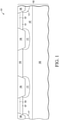
- Figure 1 sets forth a partial cutaway side view of a semiconductor wafer according to one embodiment of the present invention.
- wafer 101 includes a substrate 103 of bulk monocrystalline silicon with regions implanted with dopants and dielectric isolation structures formed therein.
- substrate 103 has a light P type dopant concentration that is formed in-situ with the formation of the substrate or implanted subsequently.
- Region 107 is formed by implanting substrate 103 with N type conductivity dopants (e.g. arsenic, phosphorous).
- N type conductivity dopants e.g. arsenic, phosphorous
- region 107 is implanted with arsenic ion dopants at a dosage of 2.5e 14 /cm 2 and an energy of 450keV, but may be implanted with other dopants, at other dosages, and/or at other energies in other embodiments.
- Region 107 is located over region 105 of substrate 103. At this time, the layers above region 107 (e.g. 135) and region 105 retain the light P dopant profile of substrate 103.
- region 117 is formed by implanting an N type conductivity dopants (e.g. arsenic) into substrate 103.
- the arsenic ion dopants for forming region 117 are implanted at a dosage of 6.2e 15 /cm 2 and an energy of 90keV, but may be implanted with other dopants, at other dosages, and/or at other energies in other embodiments.
- the opening in the mask is used to form a shallow trench isolation structure 109 of a dielectric material (e.g. silicon dioxide).
- the dielectric material may be deposited or thermally grown followed by a planarization of substrate 103.
- the partial cross sectional view of Figure 1 shows four different portions for each of isolation structure 109 and diffusion region 117. However, at other cross sections of wafer 101, (located into or out of the page from the view of Figure 1 ), structure 109 and region 117 would be contiguous across the view of Figure 1 (e.g. at end regions of a transistor). However, in other cross sectional views, the portions of structure 109 and/or the portions of region 117 shown in Figure 1 maybe physically separate from each other.
- collector regions 133, 137, 127, and 131 are formed. 2. Regions 127 and 131 are selectively implanted (through a patterned mask not shown) with a first N type dopant implant followed by a second N type dopant implant to form regions 133 and 137. Regions 133 and 137 are formed by implanting arsenic at a dosage of 6.0e 15 /cm 2 and an energy of 20keV, but may be implanted with other dopants, at other dosages, and/or at other energies.
- Regions 127 and 131 are formed by implanting phosphorous at a dosage of 1.3e 15 /cm 2 and an energy of 100keV, but may be implanted with other dopants, at other dosages, and/or at other energies. Regions 133 and 137 may also be formed separately at a later step.
- Figure 2 shows a partial cutaway side view of wafer 101 after oxide layer 201 has been formed on substrate 103 and is implanted with dopants.
- silicon oxide layer 201 is 600 angstroms thick and is deposited by a TEOS process.
- layer 201 may have other thicknesses, be deposited by other processes, and/or be made of other dielectric materials.
- layer 201 may be formed by a thermal oxidation process.
- the implanted dopants 203 are arsenic dopants.
- arsenic dopant ions 203 are implanted into the top third of layer 201 as shown by dashed line 205.
- the arsenic dopant ions may be implanted to other depths.
- the arsenic dopants implanted into the upper portion of layer 201 make the upper portion etch faster than a lower portion of layer 202 during a subsequent selective etching of layer 201. See Figure 5 and its discussion thereof.
- the arsenic dopant ions are implanted at a dosage of 5.5e 15 /cm 2 and at an energy of 10keV, but may be implanted at other dosages and/or at other energies as well.
- the dosage of the dopants may be in the range of 3.0 - 10.0e 15 /cm 2 .
- types of dopants e.g. phosphorous
- the dopants e.g. arsenic
- An arsenic precursor is introduced in the deposition chamber during the latter portion of the deposition of layer 201.
- the deposition chamber process conditions during the deposition of layer 201 may also be modified to increase the etch rate of the upper portion of layer 201 with respect to the lower portion. For example, a lower deposition temperature during the deposition of the upper portion of layer 201 may result in a less dense oxide with a higher etch in the upper portion of layer 201.
- non-conductivity dopants e.g. xenon, fluorine
- xenon, fluorine may be implanted or introduced into the upper portion of layer 201 to change the etch rate of the upper portion.
- dopants could be implanted or introduced in-situ in the lower portion of layer 201 so that the lower portion of layer 201 etches at a slower rate than the upper portion.
- boron may be introduced in the lower portion of layer 201 to slow the etch rate relative to the upper portion of layer 201.
- Figure 3 shows a partial cutaway side view of wafer 101 after a layer 301 of polysilicon is formed on layer 201 followed by the deposition of dielectric layers 303, 305, and 307.
- Layer 301 may be 600 angstroms thick, but may be of other thicknesses.
- Layer 301 is doped with conductivity dopants (e.g. boron) either in-situ or ion implanted (e.g. at a dosage of 1.4e 16 /cm 2 and at an energy of 15 keV).
- conductivity dopants e.g. boron
- layer 303 is an oxide layer (e.g. silicon oxide)
- layer 305 is a nitride layer (e.g. silicon nitride)
- layer 307 is an oxide layer
- layers 303 and 307 have a thickness of 150 angstroms and layer 305 has a thickness of 500 angstrom, but may have other thicknesses.
- Figure 4 shows a partial cutaway side view of wafer 101 after an opening 401 is formed in layers 305, 303, 301, and 307 and a nitride spacer 403 is formed on the opening side walls.
- the opening is formed by patterning a layer of photo resist or other masking material (not shown) with a corresponding opening and etching layers 301, 303, 305, and 307.
- Layer 201 is exposed through opening 401.
- the opening 401 is formed by etching layers 301, 303, 305, and 307 with the appropriate etchants.
- spacer 403 is made of silicon nitride.
- Spacer 403 is formed by forming a layer of silicon nitride (not shown) over wafer 101 and then performing a reactive ion etch to remove the portions of the silicon nitride layer located on the horizontal surfaces of wafer 101. Oxide layer 307 remains on the horizontal surfaces of wafer 101.
- Spacer 403 may be made by other processes and/or other materials.
- Figure 5 shows a partial cutaway side view of wafer 101 after a void 500 is formed in layer 201 and collector region 503 is selectively implanted through opening 401.
- Void 500 is formed in layer 201 by performing a wet etch (isotropic) through opening 401 to etch the exposed portions of layer 201. Alternatively, this wet etch is performed with hydrofluoric (HF) acid. This wet etch etches out the portion of layer 201 underneath spacer 403 and layer 301 in proximity to opening 401. Because the upper portion of layer 201 was implanted with dopants that change the etch rate, the upper portion of layer 201 (that is shown by dashed line 205 etches faster than the lower portion of layer 201 (below line 205).
- HF hydrofluoric
- the upper portion of layer 201 in which layer 201 is silicon oxide, where the upper portion of layer 201 has been implanted with arsenic at a dosage of 5.5e 15 /cm 2 , and where the etchant is HF acid, the upper portion of layer 201 etches at a rate of 1.7 times faster than the undoped portion of layer 201.
- the upper portion of layer 201 is etched at a rate that is in the range of 1.3 to 2.5 times faster than the lower portion.
- the etch rates may be different for different layer materials, different etch chemistries, or different dopants.
- layer 307 is also removed.
- the profile of side wall 501 at the upper portion of layer 201 is shown as generally planar along the upper portion above dashed line 205.
- the sidewall of the top surface of the upper portion of layer 201 may not laterally extend as far away from opening 401 as the sidewall at a lower level of the upper portion. Consequently, the widest portion of void 500 may be at a level in the upper portion of layer 201 just below the level of the top surface of layer 201.
- the doping profile in the upper portion of layer 201 may be non-uniform, with a higher concentration just below the top surface of layer 201 leading to a higher etch rate and wider void 500 just below the level of the top surface of layer 201.
- Lightly doped (or undoped) region 135 is implanted through opening 401 with N type dopant ions (e.g. arsenic, nowadays) to form an intrinsic collector region 503.
- the dopant ions may be implanted at an energy of 200keV with a dose of 7.0e 13 /cm 2 such that region 503 extends down to region 107.
- wafer 101 is annealed to activate the dopants of region 503.
- the formation of region 503 occurs after the formation of void 500, but may be performed before the formation of void 500 as an alternative.
- Figure 6 shows a partial cutaway side view of wafer 101 after a structure 601 of monocrystalline silicon germanium is grown in void 500 including underneath the portions of layer 301.
- Structure 601 may be formed by an epitaxial growth process where the silicon germanium is grown from the exposed portions of regions 135, 503 and layer 301 by the epitaxial process.
- Structure 601 may also be in-situ doped with a P type dopant (e.g. boron) at a dose of 4.7e 13 /cm 2 .
- Structure 601 may also be in-situ doped with carbon at a level of 0.04%.
- the germanium content varies from 0% to 30% within structure 601. However, structure 601 may also be formed without carbon or germanium (i.e. only P type silicon). Structure 601 can be formed by other processes and/or be made of other materials (e.g. silicon carbon).
- wafer 101 Prior to forming structure 601, wafer 101 is subjected to an HF precleaning process.
- Figure 7 shows a partial cutaway side view of wafer 101 after the formation of emitter spacer 701 and polysilicon emitter layer 703.
- spacer 701 is formed on structure 601 next to spacer 403.
- Spacer 701 may be formed by depositing layers of oxide, nitride, and the oxide (none shown) over wafer 101 and then performing a reactive ion etch to form the spacer.
- the first deposited oxide layer may be 150 angstroms, the nitride layer 200 angstroms, and the second deposited oxide layer 500 angstroms thick, but the layers may be of other thicknesses.
- wafer 101 is subjected to an HF pre-clean that removes from spacer 701, the portion formed from the second deposited oxide layer (not shown) and the remainder of the first deposited oxide layer on structure 601.
- a layer 703 of polysilicon is deposited on wafer 101.
- Layer 703 may have a thickness of 800 angstroms, but may be of other thicknesses.
- Figure 8 shows a partial cutaway side view of wafer 101 after structures of wafer 101 have been patterned twice.
- the first patterning removes the portions of layers 703, 305 and 303, shown in the view of Figure 8 , outside of area 801. Although not shown in the view of Figure 8 , similar portions of these layers would remain in other areas of wafer 101, e.g. where other semiconductor devices are being formed on wafer 101.
- These layers may be patterned by forming a patterned mask (not shown) over wafer 101 with openings outside of area 801. Layers 703, 305, and 303 are then etched (e.g. by a reactive ion etch) through the openings.
- Intrinsic emitter 803 is formed from poly silicon layer 703 as a result of the etching.
- the second patterning of wafer 101 removes the portions of layers 301 and 201 shown in the view of Figure 7 , outside of area 805. Although not shown in the view of Figure 8 , similar portions of these layers would remain in other areas of wafer 101, e.g. where other semiconductor devices are being formed on wafer 101. These layers may be patterned by forming a patterned mask (not shown) over wafer 101 with openings outside of area 805. Layers 301 and 201 are then etched (e.g. by a reactive ion etch to etch layer 301 followed by an HF wet etch to etch layer 201) through the openings.
- Base electrode structure 807 is formed by the patterning of layer 301. In the cutaway view of Figure 8 , structure 807 includes two portions located on the left and right of spacer 701 where spacer 701 and a portion of emitter 803 are located in an opening of structure 807 such that structure 807 surrounds spacer 701.
- regions 133 and 137 are formed by selectively implanting (through a patterned mask not shown) with an N type dopant implant arsenic at a dosage of 6.0e 15 /cm 2 and an energy of 20keV. Other dopants, at other dosages, and/or at other energies may be implanted, alternatively.
- Wafer 101 may be annealed at high temperate to activate and diffuse all the dopants (e.g. of intrinsic base structure 601 and intrinsic emitter 803).
- Figure 9 shows a partial cutaway side view of wafer 101 after silicide structures (901, 902, 903, and 905) are formed on the exposed silicon areas of wafer 101.
- the silicide structures are formed by depositing a layer of metal (e.g. nickel, cobalt) over wafer 101 and heating wafer 101 wherein the metal reacts with the exposed silicon to form the silicide. Afterwards, the unreacted metal is removed.
- metal e.g. nickel, cobalt
- silicide structure 901 is formed on collector contact region 133
- structure 902 is formed on base electrode structure 807
- silicide structure 903 is formed on intrinsic emitter 803
- silicide structure 905 is formed on collector contact region 137.
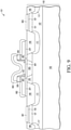
- Figure 10 shows a partial cutaway side view of wafer 101 after the formation of interconnects to the silicide structures.
- a conformal layer 1002 of dielectric material e.g. nitride
- layer 1002 has a thickness of 500 angstroms, but may be of other thicknesses.
- a relatively thick layer 1003 of oxide e.g. formed by a TEOS process
- planarized e.g. using chemical mechanical polishing. Openings are then formed in layers 1003 and 1002 to expose silicide structures 901, 902, 903, and 905.
- a layer of contact material e.g.
- tungsten, copper is formed over wafer 101 including in the openings and then planarized to form isolated plugs 1005, 1007, 1009, 1011, and 1013.
- the plugs may include barrier metal layers.
- a second dielectric layer 1015 is formed over wafer 101. Openings are formed in layer 1015 to expose conductive plugs 1005, 1007, 1009, 1011, and 1013.
- a layer of interconnect conductive material (e.g. copper) is formed over layer 1015 and subsequently planarized to form interconnect 1017, 1019, 1021, 1023, and 1025.
- the conductive material may include barrier metal layers under the copper.
- Other examples may have other conductive structures and/or may be formed in other ways.
- the conductive interconnect structures may electrically couple two or more plugs of plugs 1005, 1007, 1009, 1011, and 1013.
- Collector plugs 1005 and 1013 may be electrically coupled.
- the transistor formed in wafer 101 is a bipolar NPN transistor where region 503 is the intrinsic collector and structure 601 is the intrinsic base along with intrinsic emitter 803.
- Intrinsic base structure 601 is electrically accessible from interconnect 1023 via plug 1011, silicide structure 902, and base electrode structure 807 as well as from interconnect 1019 via plug 1007 and silicide structure 902.
- Intrinsic emitter 803 is accessible by interconnect 1021, plug 1009, and silicide structure 903.
- Intrinsic collector region 503 is electrically accessible from interconnect 1025 by plug 1013, silicide structure 905, collector contact region 137, and intermediate collector regions 131, 107, and 117.
- Intrinsic collector region 503 is also electrically accessible from interconnect 1017 by plug 1005, silicide structure 901, collector contact region 133, and intermediate collector regions 127, 107, and 117.
- Regions 113 and 137 are physically separated from each other and are implemented in "finger structures" located along isolation structure 109 opposite each side of collector region 503.
- regions 133 and 137 may also be physically connected at other locations of wafer 101 (e.g. at an end region of the transistor).
- the processes herein may be utilized in forming other types of semiconductor devices such as a PNP bipolar transistor, MOSFET, or diode.
- a PNP bipolar transistor the P type doped regions and the N type doped regions would be switched from the device of Figure 10 .
- interconnect structures may be formed over layer 1015.
- External connectors such as bond pads would be formed on wafer 101.
- wafer 101 is singulated into multiple die with each die including one or more transistors as shown in Figure 10 .
- the die are packaged in semiconductor packages (e.g. leaded, leadless, BGA, QFN, QFP, or wafer level package).
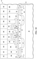
- Figure 11 shows a close up view of the partial cutaway view of Figure 10 .
- Figure 11 shows the distance 1111 that intrinsic base structure 601 extends underneath base electrode structure 807.
- the base resistance between base electrode structure 807 and intrinsic base structure 601 is dependent upon distance 1111, with a greater distance providing for a decrease in resistance.
- the capacitance between the intrinsic base structure 601 and collector region 503 is dependent upon the width 1113 with a smaller width providing for a decrease in capacitance.
- minimizing the width may improve transistor performance in some embodiments by decreasing the base collector capacitance.
- Providing a layer of dielectric material with an upper portion and a lower portion having different etch rate properties enables for the formation of an intrinsic base structure with a wider upper portion to decrease the base resistance and a narrower lower portion to decrease the base collector capacitance.
- Such an intrinsic base region is formed with a sacrificial dielectric layer having an upper portion and a lower portion that are each etched with the same etchant as opposed to using two layers of different materials. Such methods may reduce the complexity of manufacture of such devices.
- transistors structures described herein can be formed with BICMOS processes, but may be formed by other processes in other embodiments.
- region 503 is underneath structure 601. Although region 503 is at a level of being below the level of layer 201, it is not underneath layer 201.
- intrasic emitter is the structures of a bipolar device that form the PN junctions (the collector/base junction and the base/emitter junction) of the bipolar transistor.
- the forming of the layer of dielectric material includes in-situ doping the upper portion with dopants to provide the upper portion of the layer of dielectric material with a higher concentration of the dopants than the lower portion of the layer of dielectric material to provide the upper portion with the first etch rate property with respect to the second etch rate property.
- the semiconductor device includes a second structure of semiconductor material underneath and in contact with the structure of semiconductor material, wherein the structure of semiconductor material has a first conductivity doping profile that is opposite a conductivity doping profile of the second structure of semiconductor material.
- the structure of semiconductor material is characterized as an intrinsic base of the semiconductor device and the second structure of semiconductor material is characterized as an intrinsic collector of the semiconductor device.
- the second structure of semiconductor material includes conductivity dopants implanted into a layer of semiconductor material through the opening.
Claims (11)
- Procédé de formation d'un dispositif à semi-conducteur, comprenant :former une couche (201) de matériau diélectrique, où une partie supérieure de la couche (201) de matériau diélectrique a une première vitesse de gravure par rapport à un agent de gravure et une partie inférieure de la couche (201) de matériau diélectrique a une seconde vitesse de gravure par rapport à l'agent de gravure ;former une couche (301) de matériau semi-conducteur sur la couche (201) de matériau diélectrique ;former une ouverture (401) dans la couche (301) de matériau semi-conducteur et exposer la couche (201) de matériau diélectrique à travers l'ouverture ;graver, avec l'agent de gravure, la couche (201) de matériau diélectrique à travers l'ouverture pour enlever une partie de la couche (201) de matériau diélectrique sous la couche (301) de matériau semi-conducteur avec l'agent de gravure, où la partie supérieure de la couche (201) de matériau diélectrique est enlevée par gravure avec l'agent de gravure à une vitesse plus rapide que la partie inférieure de la couche (201) de matériau diélectrique est enlevée par la gravure avec l'agent de gravure de sorte qu'une paroi latérale restante (501) de la couche (201) de matériau diélectrique définie par la gravure sous la couche (301) de matériau semi-conducteur est non plane, avec une partie supérieure de la paroi latérale restante (501) s'étendant latéralement plus loin de l'ouverture qu'une partie inférieure de la paroi latérale restante (501) s'étendant latéralement de l'ouverture ;former une structure (601) de matériau semi-conducteur dans un emplacement où la couche (201) de matériau diélectrique a été retirée par la gravure, où la structure s'étend sous la couche (301) de matériau semi-conducteur pour entrer en contact avec une surface inférieure de la couche (301) de matériau semi-conducteur sous la couche (301) de matériau semi-conducteur, la structure ayant une paroi latérale de structure avec une partie supérieure correspondant à la partie supérieure de la paroi latérale restante (501) qui s'étend plus loin sous la couche (301) de matériau semi-conducteur qu'une partie inférieure de la paroi latérale de structure qui correspond à la partie inférieure de la paroi latérale restante (501),caractérisé en ce que la formation de la couche (201) de matériau diélectrique comprend :
l'introduction in situ de dopants pendant la dernière partie du dépôt de ladite couche de matériau diélectrique (201), pour fournir à la partie supérieure de la couche (201) de matériau diélectrique une concentration plus élevée de dopants (203) que la partie inférieure de la couche (201) de matériau diélectrique, de sorte que la première vitesse de gravure est plus rapide que la seconde vitesse de gravure. - Procédé selon la revendication 1, dans lequel le dispositif à semi-conducteur comprend une deuxième structure (503) de matériau semi-conducteur en dessous et en contact avec la structure (601) de matériau semi-conducteur, où la structure (601) de matériau semi-conducteur a un premier profil de dopage de conductivité qui est opposé à un profil de dopage de conductivité de la deuxième structure (503) de matériau semi-conducteur.
- Procédé selon la revendication 2, dans lequel la structure (601) de matériau semi-conducteur est caractérisée comme une base intrinsèque du dispositif à semi-conducteur et la deuxième structure (503) de matériau semi-conducteur est caractérisée comme un collecteur intrinsèque du dispositif à semi-conducteur.
- Procédé selon la revendication 2 ou la revendication 3, dans lequel la deuxième structure (503) de matériau semi-conducteur comprend des dopants de conductivité (203) implantés dans une couche (301) de matériau semi-conducteur à travers l'ouverture.
- Procédé selon l'une quelconque des revendications précédentes, dans lequel la structure (601) de matériau semi-conducteur est caractérisée comme une base intrinsèque du dispositif à semi-conducteur, où une partie de la couche (301) de matériau semi-conducteur dans laquelle la structure (601) de matériau semi-conducteur est située en dessous est caractérisée comme une électrode de base du dispositif à semi-conducteur.
- Procédé selon l'une quelconque des revendications précédentes, dans lequel la première vitesse de gravure se situe dans une plage 1,3 à 2,5 fois plus rapide que la seconde vitesse de gravure.
- Procédé selon l'une quelconque des revendications précédentes, dans lequel le matériau diélectrique est de l'oxyde de silicium et les dopants (203) comprennent de l'arsenic.
- Procédé selon l'une quelconque des revendications précédentes, dans lequel, après avoir formé la structure (601) de matériau semi-conducteur, il est formé une troisième structure (803) de matériau semi-conducteur sur la structure et en contact avec celle-ci, où au moins une partie de la troisième structure (803) est située dans l'ouverture, où la structure (601) de matériau semi-conducteur est caractérisée comme une base intrinsèque du dispositif à semi-conducteur et la troisième structure (803) est caractérisée comme un émetteur intrinsèque du dispositif à semi-conducteur.
- Dispositif à semi-conducteur, comprenant :une première structure semi-conductrice (601) ;une deuxième structure semi-conductrice (301) ayant une première paroi latérale, une partie de la première structure semi-conductrice (601) s'étendant sous la deuxième structure semi-conductrice (301) depuis la première paroi latérale et ayant une surface supérieure en contact avec une surface inférieure de la deuxième structure semi-conductrice (301) sous la deuxième structure semi-conductrice (301) ;une couche (201) de matériau diélectrique sous la deuxième structure semi-conductrice (301), la couche (201) de matériau diélectrique ayant une deuxième paroi latérale (501) en contact latéral avec la partie de la première structure semi-conductrice (601), où la première structure semi-conductrice (601) a une partie supérieure et une partie inférieure, où la partie supérieure est plus large que la partie inférieure, où la partie supérieure de la première structure semi-conductrice (601) est en contact avec une partie supérieure de la couche (201) de matériau diélectrique au niveau de la deuxième paroi latérale (501) et la partie inférieure de la première structure semi-conductrice (601) est en contact avec une partie inférieure de la couche (201) de matériau diélectrique au niveau de la deuxième paroi latérale (501), où la partie supérieure de la couche (201) de matériau diélectrique est attaquée à une première vitesse d'attaque avec un agent d'attaque et la partie inférieure de la couche (201) de matériau diélectrique est attaquée à une seconde vitesse d'attaque avec l'agent d'attaque,caractérisé en ce que la partie supérieure de la couche (201) de matériau diélectrique a une concentration plus élevée de dopants (203) que la partie inférieure de la couche (201) de matériau diélectrique, de sorte que la première vitesse de gravure est plus rapide que la seconde vitesse de gravure, la concentration plus élevée de dopants résultant d'une introduction in situ de dopants avec la formation de la couche (201) pendant la dernière partie du dépôt de la couche de matériau diélectrique (201).
- Dispositif à semi-conducteur selon la revendication 9, dans lequel le matériau diélectrique est de l'oxyde de silicium et les dopants (203) comprennent de l'arsenic.
- Dispositif à semi-conducteur selon la revendication 9 ou la revendication 10, dans lequel la première structure semi-conductrice (601) est caractérisée comme une base intrinsèque d'un transistor bipolaire, et la deuxième structure semi-conductrice (301) est caractérisée comme une électrode de base (807) du dispositif à semi-conducteur, où le dispositif à semi-conducteur comprend un collecteur intrinsèque (503) situé sous la base intrinsèque.
Applications Claiming Priority (1)
| Application Number | Priority Date | Filing Date | Title |
|---|---|---|---|
| US15/286,988 US9786770B1 (en) | 2016-10-06 | 2016-10-06 | Semiconductor device structure with non planar slide wall |
Publications (2)
| Publication Number | Publication Date |
|---|---|
| EP3306670A1 EP3306670A1 (fr) | 2018-04-11 |
| EP3306670B1 true EP3306670B1 (fr) | 2022-03-23 |
Family
ID=59381129
Family Applications (1)
| Application Number | Title | Priority Date | Filing Date |
|---|---|---|---|
| EP17181954.3A Active EP3306670B1 (fr) | 2016-10-06 | 2017-07-18 | Structure de dispositif semi-conducteur ayant une paroi latérale non plane et méthode de fabrication utilisant un diélectrique doté |
Country Status (3)
| Country | Link |
|---|---|
| US (2) | US9786770B1 (fr) |
| EP (1) | EP3306670B1 (fr) |
| CN (1) | CN107919281B (fr) |
Families Citing this family (5)
| Publication number | Priority date | Publication date | Assignee | Title |
|---|---|---|---|---|
| JP6649216B2 (ja) * | 2016-09-16 | 2020-02-19 | 株式会社東芝 | 半導体装置およびその製造方法 |
| US11183587B2 (en) * | 2019-10-31 | 2021-11-23 | Taiwan Semiconductor Manufacturing Company, Ltd. | Bipolar junction transistor (BJT) comprising a multilayer base dielectric film |
| DE102020118776A1 (de) * | 2019-10-31 | 2021-05-20 | Taiwan Semiconductor Manufacturing Co., Ltd. | Bipolartransistor (bjt) mit einem dielektrischen mehrschichtbasisfilm |
| US11545577B2 (en) * | 2020-12-08 | 2023-01-03 | Globalfoundries U.S. Inc. | Semiconductor structure with in-device high resistivity polycrystalline semiconductor element and method |
| US20230361204A1 (en) * | 2022-05-04 | 2023-11-09 | Taiwan Semiconductor Manufacturing Company, Ltd. | Bipolar junction transistors and methods of forming the same |
Family Cites Families (14)
| Publication number | Priority date | Publication date | Assignee | Title |
|---|---|---|---|---|
| US5316965A (en) | 1993-07-29 | 1994-05-31 | Digital Equipment Corporation | Method of decreasing the field oxide etch rate in isolation technology |
| US6521974B1 (en) * | 1999-10-14 | 2003-02-18 | Hitachi, Ltd. | Bipolar transistor and manufacturing method thereof |
| TW492082B (en) | 2000-12-19 | 2002-06-21 | Taiwan Semiconductor Mfg | Method to increase wet etching rate of dielectric layer using ion implantation |
| US7075126B2 (en) * | 2004-02-27 | 2006-07-11 | International Business Machines Corporation | Transistor structure with minimized parasitics and method of fabricating the same |
| DE102004061327A1 (de) | 2004-12-11 | 2006-06-14 | IHP GmbH - Innovations for High Performance Microelectronics/Institut für innovative Mikroelektronik | Vertikaler Bipolartransistor |
| US7598539B2 (en) * | 2007-06-01 | 2009-10-06 | Infineon Technologies Ag | Heterojunction bipolar transistor and method for making same |
| US7816221B2 (en) * | 2008-06-26 | 2010-10-19 | Freescale Semiconductor, Inc. | Dielectric ledge for high frequency devices |
| DE102009001552A1 (de) | 2008-12-12 | 2010-06-17 | Ihp Gmbh - Innovations For High Performance Microelectronics / Leibniz-Institut Für Innovative Mikroelektronik | Bipolartransistor mit selbstjustiertem Emitterkontakt |
| JP2011243657A (ja) * | 2010-05-14 | 2011-12-01 | Mitsumi Electric Co Ltd | 半導体装置の製造方法 |
| KR101062862B1 (ko) * | 2010-07-07 | 2011-09-07 | 주식회사 하이닉스반도체 | 측벽접합을 구비한 반도체장치 제조 방법 |
| CN102456727A (zh) | 2010-10-25 | 2012-05-16 | 上海华虹Nec电子有限公司 | 低集电极/基极电容SiGe异质结双极晶体管结构及制造方法 |
| US8610174B2 (en) | 2011-11-30 | 2013-12-17 | International Business Machines Corporation | Bipolar transistor with a raised collector pedestal for reduced capacitance |
| JP2014199864A (ja) * | 2013-03-29 | 2014-10-23 | 住友電工デバイス・イノベーション株式会社 | 半導体装置及びその製造方法 |
| DE102014113989B4 (de) * | 2014-09-26 | 2020-06-04 | Infineon Technologies Ag | Verfahren zur Herstellung eines Bipolartransistors |
-
2016
- 2016-10-06 US US15/286,988 patent/US9786770B1/en active Active
-
2017
- 2017-07-18 EP EP17181954.3A patent/EP3306670B1/fr active Active
- 2017-08-14 US US15/675,852 patent/US10269943B2/en active Active
- 2017-09-27 CN CN201710889299.4A patent/CN107919281B/zh active Active
Non-Patent Citations (1)
| Title |
|---|
| None * |
Also Published As
| Publication number | Publication date |
|---|---|
| US10269943B2 (en) | 2019-04-23 |
| US20180102421A1 (en) | 2018-04-12 |
| US9786770B1 (en) | 2017-10-10 |
| EP3306670A1 (fr) | 2018-04-11 |
| CN107919281B (zh) | 2022-09-06 |
| CN107919281A (zh) | 2018-04-17 |
Similar Documents
| Publication | Publication Date | Title |
|---|---|---|
| EP3306670B1 (fr) | Structure de dispositif semi-conducteur ayant une paroi latérale non plane et méthode de fabrication utilisant un diélectrique doté | |
| US6355533B2 (en) | Method for manufacturing semiconductor device | |
| US8569840B2 (en) | Bipolar transistor integrated with metal gate CMOS devices | |
| KR101251309B1 (ko) | 트렌치 구조들을 가진 반도체 장치 및 이의 제조방법 | |
| KR100282452B1 (ko) | 반도체 소자 및 그의 제조 방법 | |
| US7465969B2 (en) | Bipolar transistor and method for fabricating the same | |
| KR20020039319A (ko) | 반도체장치 및 그 제조방법 | |
| JP2009523326A (ja) | ゲートの頂部が拡張された半導体トランジスタ | |
| US7456070B2 (en) | Method of fabricating a bipolar transistor with high breakdown voltage collector | |
| US6639282B2 (en) | Semiconductor device on silicon-on-insulator and method for manufacturing the semiconductor device | |
| US6254676B1 (en) | Method for manufacturing metal oxide semiconductor transistor having raised source/drain | |
| JP4514023B2 (ja) | ソース/ドレイン拡張部からドーパントが外方拡散しないようにするための、シリコン酸化物ライナーのイオン注入 | |
| US20090152670A1 (en) | Semiconductor device and method of fabricating the same | |
| US7402487B2 (en) | Process for fabricating a semiconductor device having deep trench structures | |
| KR100497877B1 (ko) | 단단계 임플랜테이션을 이용한 자체 정렬 엘디디를 이용하여 형성되는 트랜지스터 | |
| US6774455B2 (en) | Semiconductor device with a collector contact in a depressed well-region | |
| US6489211B1 (en) | Method of manufacturing a semiconductor component | |
| JP2002543609A (ja) | シャロージャンクション半導体デバイスの製造方法 | |
| JP2007067425A (ja) | 半導体装置の製造方法 | |
| US6797578B1 (en) | Method for fabrication of emitter of a transistor and related structure | |
| KR100200757B1 (ko) | 반도체소자 및 그 제조방법 | |
| US6936514B1 (en) | Semiconductor component and method | |
| JP2005026707A (ja) | 半導体装置及びその製造方法 | |
| US11640975B2 (en) | Silicided collector structure | |
| US20240079473A1 (en) | Method for forming a transistor with a conductivity doped base structure |
Legal Events
| Date | Code | Title | Description |
|---|---|---|---|
| PUAI | Public reference made under article 153(3) epc to a published international application that has entered the european phase |
Free format text: ORIGINAL CODE: 0009012 |
|
| STAA | Information on the status of an ep patent application or granted ep patent |
Free format text: STATUS: THE APPLICATION HAS BEEN PUBLISHED |
|
| AK | Designated contracting states |
Kind code of ref document: A1 Designated state(s): AL AT BE BG CH CY CZ DE DK EE ES FI FR GB GR HR HU IE IS IT LI LT LU LV MC MK MT NL NO PL PT RO RS SE SI SK SM TR |
|
| AX | Request for extension of the european patent |
Extension state: BA ME |
|
| STAA | Information on the status of an ep patent application or granted ep patent |
Free format text: STATUS: REQUEST FOR EXAMINATION WAS MADE |
|
| 17P | Request for examination filed |
Effective date: 20181011 |
|
| RBV | Designated contracting states (corrected) |
Designated state(s): AL AT BE BG CH CY CZ DE DK EE ES FI FR GB GR HR HU IE IS IT LI LT LU LV MC MK MT NL NO PL PT RO RS SE SI SK SM TR |
|
| STAA | Information on the status of an ep patent application or granted ep patent |
Free format text: STATUS: EXAMINATION IS IN PROGRESS |
|
| STAA | Information on the status of an ep patent application or granted ep patent |
Free format text: STATUS: EXAMINATION IS IN PROGRESS |
|
| 17Q | First examination report despatched |
Effective date: 20201009 |
|
| REG | Reference to a national code |
Ref country code: DE Ref legal event code: R079 Ref document number: 602017054852 Country of ref document: DE Free format text: PREVIOUS MAIN CLASS: H01L0029660000 Ipc: H01L0021311500 |
|
| RIC1 | Information provided on ipc code assigned before grant |
Ipc: H01L 29/737 20060101ALN20210803BHEP Ipc: H01L 29/08 20060101ALN20210803BHEP Ipc: H01L 29/10 20060101ALI20210803BHEP Ipc: H01L 29/06 20060101ALI20210803BHEP Ipc: H01L 29/732 20060101ALI20210803BHEP Ipc: H01L 21/331 20060101ALI20210803BHEP Ipc: H01L 21/311 20060101ALI20210803BHEP Ipc: H01L 21/3115 20060101AFI20210803BHEP |
|
| GRAP | Despatch of communication of intention to grant a patent |
Free format text: ORIGINAL CODE: EPIDOSNIGR1 |
|
| STAA | Information on the status of an ep patent application or granted ep patent |
Free format text: STATUS: GRANT OF PATENT IS INTENDED |
|
| RIC1 | Information provided on ipc code assigned before grant |
Ipc: H01L 29/737 20060101ALN20210908BHEP Ipc: H01L 29/08 20060101ALN20210908BHEP Ipc: H01L 29/10 20060101ALI20210908BHEP Ipc: H01L 29/06 20060101ALI20210908BHEP Ipc: H01L 29/732 20060101ALI20210908BHEP Ipc: H01L 21/331 20060101ALI20210908BHEP Ipc: H01L 21/311 20060101ALI20210908BHEP Ipc: H01L 21/3115 20060101AFI20210908BHEP |
|
| GRAJ | Information related to disapproval of communication of intention to grant by the applicant or resumption of examination proceedings by the epo deleted |
Free format text: ORIGINAL CODE: EPIDOSDIGR1 |
|
| GRAP | Despatch of communication of intention to grant a patent |
Free format text: ORIGINAL CODE: EPIDOSNIGR1 |
|
| STAA | Information on the status of an ep patent application or granted ep patent |
Free format text: STATUS: GRANT OF PATENT IS INTENDED |
|
| INTG | Intention to grant announced |
Effective date: 20211013 |
|
| INTG | Intention to grant announced |
Effective date: 20211027 |
|
| GRAS | Grant fee paid |
Free format text: ORIGINAL CODE: EPIDOSNIGR3 |
|
| GRAA | (expected) grant |
Free format text: ORIGINAL CODE: 0009210 |
|
| STAA | Information on the status of an ep patent application or granted ep patent |
Free format text: STATUS: THE PATENT HAS BEEN GRANTED |
|
| AK | Designated contracting states |
Kind code of ref document: B1 Designated state(s): AL AT BE BG CH CY CZ DE DK EE ES FI FR GB GR HR HU IE IS IT LI LT LU LV MC MK MT NL NO PL PT RO RS SE SI SK SM TR |
|
| REG | Reference to a national code |
Ref country code: GB Ref legal event code: FG4D |
|
| REG | Reference to a national code |
Ref country code: CH Ref legal event code: EP |
|
| REG | Reference to a national code |
Ref country code: IE Ref legal event code: FG4D |
|
| REG | Reference to a national code |
Ref country code: DE Ref legal event code: R096 Ref document number: 602017054852 Country of ref document: DE |
|
| REG | Reference to a national code |
Ref country code: AT Ref legal event code: REF Ref document number: 1478037 Country of ref document: AT Kind code of ref document: T Effective date: 20220415 |
|
| REG | Reference to a national code |
Ref country code: LT Ref legal event code: MG9D |
|
| REG | Reference to a national code |
Ref country code: NL Ref legal event code: MP Effective date: 20220323 |
|
| PG25 | Lapsed in a contracting state [announced via postgrant information from national office to epo] |
Ref country code: SE Free format text: LAPSE BECAUSE OF FAILURE TO SUBMIT A TRANSLATION OF THE DESCRIPTION OR TO PAY THE FEE WITHIN THE PRESCRIBED TIME-LIMIT Effective date: 20220323 Ref country code: RS Free format text: LAPSE BECAUSE OF FAILURE TO SUBMIT A TRANSLATION OF THE DESCRIPTION OR TO PAY THE FEE WITHIN THE PRESCRIBED TIME-LIMIT Effective date: 20220323 Ref country code: NO Free format text: LAPSE BECAUSE OF FAILURE TO SUBMIT A TRANSLATION OF THE DESCRIPTION OR TO PAY THE FEE WITHIN THE PRESCRIBED TIME-LIMIT Effective date: 20220623 Ref country code: LT Free format text: LAPSE BECAUSE OF FAILURE TO SUBMIT A TRANSLATION OF THE DESCRIPTION OR TO PAY THE FEE WITHIN THE PRESCRIBED TIME-LIMIT Effective date: 20220323 Ref country code: HR Free format text: LAPSE BECAUSE OF FAILURE TO SUBMIT A TRANSLATION OF THE DESCRIPTION OR TO PAY THE FEE WITHIN THE PRESCRIBED TIME-LIMIT Effective date: 20220323 Ref country code: BG Free format text: LAPSE BECAUSE OF FAILURE TO SUBMIT A TRANSLATION OF THE DESCRIPTION OR TO PAY THE FEE WITHIN THE PRESCRIBED TIME-LIMIT Effective date: 20220623 |
|
| REG | Reference to a national code |
Ref country code: AT Ref legal event code: MK05 Ref document number: 1478037 Country of ref document: AT Kind code of ref document: T Effective date: 20220323 |
|
| PG25 | Lapsed in a contracting state [announced via postgrant information from national office to epo] |
Ref country code: LV Free format text: LAPSE BECAUSE OF FAILURE TO SUBMIT A TRANSLATION OF THE DESCRIPTION OR TO PAY THE FEE WITHIN THE PRESCRIBED TIME-LIMIT Effective date: 20220323 Ref country code: GR Free format text: LAPSE BECAUSE OF FAILURE TO SUBMIT A TRANSLATION OF THE DESCRIPTION OR TO PAY THE FEE WITHIN THE PRESCRIBED TIME-LIMIT Effective date: 20220624 Ref country code: FI Free format text: LAPSE BECAUSE OF FAILURE TO SUBMIT A TRANSLATION OF THE DESCRIPTION OR TO PAY THE FEE WITHIN THE PRESCRIBED TIME-LIMIT Effective date: 20220323 |
|
| PG25 | Lapsed in a contracting state [announced via postgrant information from national office to epo] |
Ref country code: NL Free format text: LAPSE BECAUSE OF FAILURE TO SUBMIT A TRANSLATION OF THE DESCRIPTION OR TO PAY THE FEE WITHIN THE PRESCRIBED TIME-LIMIT Effective date: 20220323 |
|
| PG25 | Lapsed in a contracting state [announced via postgrant information from national office to epo] |
Ref country code: SM Free format text: LAPSE BECAUSE OF FAILURE TO SUBMIT A TRANSLATION OF THE DESCRIPTION OR TO PAY THE FEE WITHIN THE PRESCRIBED TIME-LIMIT Effective date: 20220323 Ref country code: SK Free format text: LAPSE BECAUSE OF FAILURE TO SUBMIT A TRANSLATION OF THE DESCRIPTION OR TO PAY THE FEE WITHIN THE PRESCRIBED TIME-LIMIT Effective date: 20220323 Ref country code: RO Free format text: LAPSE BECAUSE OF FAILURE TO SUBMIT A TRANSLATION OF THE DESCRIPTION OR TO PAY THE FEE WITHIN THE PRESCRIBED TIME-LIMIT Effective date: 20220323 Ref country code: PT Free format text: LAPSE BECAUSE OF FAILURE TO SUBMIT A TRANSLATION OF THE DESCRIPTION OR TO PAY THE FEE WITHIN THE PRESCRIBED TIME-LIMIT Effective date: 20220725 Ref country code: ES Free format text: LAPSE BECAUSE OF FAILURE TO SUBMIT A TRANSLATION OF THE DESCRIPTION OR TO PAY THE FEE WITHIN THE PRESCRIBED TIME-LIMIT Effective date: 20220323 Ref country code: EE Free format text: LAPSE BECAUSE OF FAILURE TO SUBMIT A TRANSLATION OF THE DESCRIPTION OR TO PAY THE FEE WITHIN THE PRESCRIBED TIME-LIMIT Effective date: 20220323 Ref country code: CZ Free format text: LAPSE BECAUSE OF FAILURE TO SUBMIT A TRANSLATION OF THE DESCRIPTION OR TO PAY THE FEE WITHIN THE PRESCRIBED TIME-LIMIT Effective date: 20220323 Ref country code: AT Free format text: LAPSE BECAUSE OF FAILURE TO SUBMIT A TRANSLATION OF THE DESCRIPTION OR TO PAY THE FEE WITHIN THE PRESCRIBED TIME-LIMIT Effective date: 20220323 |
|
| PG25 | Lapsed in a contracting state [announced via postgrant information from national office to epo] |
Ref country code: PL Free format text: LAPSE BECAUSE OF FAILURE TO SUBMIT A TRANSLATION OF THE DESCRIPTION OR TO PAY THE FEE WITHIN THE PRESCRIBED TIME-LIMIT Effective date: 20220323 Ref country code: IS Free format text: LAPSE BECAUSE OF FAILURE TO SUBMIT A TRANSLATION OF THE DESCRIPTION OR TO PAY THE FEE WITHIN THE PRESCRIBED TIME-LIMIT Effective date: 20220723 Ref country code: AL Free format text: LAPSE BECAUSE OF FAILURE TO SUBMIT A TRANSLATION OF THE DESCRIPTION OR TO PAY THE FEE WITHIN THE PRESCRIBED TIME-LIMIT Effective date: 20220323 |
|
| REG | Reference to a national code |
Ref country code: DE Ref legal event code: R097 Ref document number: 602017054852 Country of ref document: DE |
|
| PLBE | No opposition filed within time limit |
Free format text: ORIGINAL CODE: 0009261 |
|
| STAA | Information on the status of an ep patent application or granted ep patent |
Free format text: STATUS: NO OPPOSITION FILED WITHIN TIME LIMIT |
|
| PG25 | Lapsed in a contracting state [announced via postgrant information from national office to epo] |
Ref country code: DK Free format text: LAPSE BECAUSE OF FAILURE TO SUBMIT A TRANSLATION OF THE DESCRIPTION OR TO PAY THE FEE WITHIN THE PRESCRIBED TIME-LIMIT Effective date: 20220323 |
|
| PG25 | Lapsed in a contracting state [announced via postgrant information from national office to epo] |
Ref country code: MC Free format text: LAPSE BECAUSE OF FAILURE TO SUBMIT A TRANSLATION OF THE DESCRIPTION OR TO PAY THE FEE WITHIN THE PRESCRIBED TIME-LIMIT Effective date: 20220323 |
|
| REG | Reference to a national code |
Ref country code: CH Ref legal event code: PL |
|
| 26N | No opposition filed |
Effective date: 20230102 |
|
| GBPC | Gb: european patent ceased through non-payment of renewal fee |
Effective date: 20220718 |
|
| REG | Reference to a national code |
Ref country code: BE Ref legal event code: MM Effective date: 20220731 |
|
| PG25 | Lapsed in a contracting state [announced via postgrant information from national office to epo] |
Ref country code: LU Free format text: LAPSE BECAUSE OF NON-PAYMENT OF DUE FEES Effective date: 20220718 Ref country code: LI Free format text: LAPSE BECAUSE OF NON-PAYMENT OF DUE FEES Effective date: 20220731 Ref country code: FR Free format text: LAPSE BECAUSE OF NON-PAYMENT OF DUE FEES Effective date: 20220731 Ref country code: CH Free format text: LAPSE BECAUSE OF NON-PAYMENT OF DUE FEES Effective date: 20220731 |
|
| PG25 | Lapsed in a contracting state [announced via postgrant information from national office to epo] |
Ref country code: SI Free format text: LAPSE BECAUSE OF FAILURE TO SUBMIT A TRANSLATION OF THE DESCRIPTION OR TO PAY THE FEE WITHIN THE PRESCRIBED TIME-LIMIT Effective date: 20220323 Ref country code: GB Free format text: LAPSE BECAUSE OF NON-PAYMENT OF DUE FEES Effective date: 20220718 Ref country code: BE Free format text: LAPSE BECAUSE OF NON-PAYMENT OF DUE FEES Effective date: 20220731 |
|
| PG25 | Lapsed in a contracting state [announced via postgrant information from national office to epo] |
Ref country code: IT Free format text: LAPSE BECAUSE OF FAILURE TO SUBMIT A TRANSLATION OF THE DESCRIPTION OR TO PAY THE FEE WITHIN THE PRESCRIBED TIME-LIMIT Effective date: 20220323 Ref country code: IE Free format text: LAPSE BECAUSE OF NON-PAYMENT OF DUE FEES Effective date: 20220718 |
|
| P01 | Opt-out of the competence of the unified patent court (upc) registered |
Effective date: 20230725 |
|
| PGFP | Annual fee paid to national office [announced via postgrant information from national office to epo] |
Ref country code: DE Payment date: 20230620 Year of fee payment: 7 |
|
| PG25 | Lapsed in a contracting state [announced via postgrant information from national office to epo] |
Ref country code: HU Free format text: LAPSE BECAUSE OF FAILURE TO SUBMIT A TRANSLATION OF THE DESCRIPTION OR TO PAY THE FEE WITHIN THE PRESCRIBED TIME-LIMIT; INVALID AB INITIO Effective date: 20170718 |
|
| PG25 | Lapsed in a contracting state [announced via postgrant information from national office to epo] |
Ref country code: MK Free format text: LAPSE BECAUSE OF FAILURE TO SUBMIT A TRANSLATION OF THE DESCRIPTION OR TO PAY THE FEE WITHIN THE PRESCRIBED TIME-LIMIT Effective date: 20220323 Ref country code: CY Free format text: LAPSE BECAUSE OF FAILURE TO SUBMIT A TRANSLATION OF THE DESCRIPTION OR TO PAY THE FEE WITHIN THE PRESCRIBED TIME-LIMIT Effective date: 20220323 |