EP3304690B1 - Wireless power transfer using direct field penetration through a metal object - Google Patents
Wireless power transfer using direct field penetration through a metal object Download PDFInfo
- Publication number
- EP3304690B1 EP3304690B1 EP16730122.5A EP16730122A EP3304690B1 EP 3304690 B1 EP3304690 B1 EP 3304690B1 EP 16730122 A EP16730122 A EP 16730122A EP 3304690 B1 EP3304690 B1 EP 3304690B1
- Authority
- EP
- European Patent Office
- Prior art keywords
- receiving element
- metal layer
- power receiving
- magnetic field
- power
- Prior art date
- Legal status (The legal status is an assumption and is not a legal conclusion. Google has not performed a legal analysis and makes no representation as to the accuracy of the status listed.)
- Active
Links
Images


Classifications
-
- H—ELECTRICITY
- H01—ELECTRIC ELEMENTS
- H01Q—ANTENNAS, i.e. RADIO AERIALS
- H01Q1/00—Details of, or arrangements associated with, antennas
- H01Q1/12—Supports; Mounting means
- H01Q1/22—Supports; Mounting means by structural association with other equipment or articles
- H01Q1/24—Supports; Mounting means by structural association with other equipment or articles with receiving set
- H01Q1/241—Supports; Mounting means by structural association with other equipment or articles with receiving set used in mobile communications, e.g. GSM
- H01Q1/242—Supports; Mounting means by structural association with other equipment or articles with receiving set used in mobile communications, e.g. GSM specially adapted for hand-held use
- H01Q1/243—Supports; Mounting means by structural association with other equipment or articles with receiving set used in mobile communications, e.g. GSM specially adapted for hand-held use with built-in antennas
-
- H—ELECTRICITY
- H01—ELECTRIC ELEMENTS
- H01Q—ANTENNAS, i.e. RADIO AERIALS
- H01Q13/00—Waveguide horns or mouths; Slot antennas; Leaky-waveguide antennas; Equivalent structures causing radiation along the transmission path of a guided wave
- H01Q13/10—Resonant slot antennas
-
- H—ELECTRICITY
- H02—GENERATION; CONVERSION OR DISTRIBUTION OF ELECTRIC POWER
- H02J—CIRCUIT ARRANGEMENTS OR SYSTEMS FOR SUPPLYING OR DISTRIBUTING ELECTRIC POWER; SYSTEMS FOR STORING ELECTRIC ENERGY
- H02J50/00—Circuit arrangements or systems for wireless supply or distribution of electric power
- H02J50/10—Circuit arrangements or systems for wireless supply or distribution of electric power using inductive coupling
- H02J50/12—Circuit arrangements or systems for wireless supply or distribution of electric power using inductive coupling of the resonant type
-
- H—ELECTRICITY
- H02—GENERATION; CONVERSION OR DISTRIBUTION OF ELECTRIC POWER
- H02J—CIRCUIT ARRANGEMENTS OR SYSTEMS FOR SUPPLYING OR DISTRIBUTING ELECTRIC POWER; SYSTEMS FOR STORING ELECTRIC ENERGY
- H02J50/00—Circuit arrangements or systems for wireless supply or distribution of electric power
- H02J50/80—Circuit arrangements or systems for wireless supply or distribution of electric power involving the exchange of data, concerning supply or distribution of electric power, between transmitting devices and receiving devices
-
- H—ELECTRICITY
- H02—GENERATION; CONVERSION OR DISTRIBUTION OF ELECTRIC POWER
- H02J—CIRCUIT ARRANGEMENTS OR SYSTEMS FOR SUPPLYING OR DISTRIBUTING ELECTRIC POWER; SYSTEMS FOR STORING ELECTRIC ENERGY
- H02J7/00—Circuit arrangements for charging or depolarising batteries or for supplying loads from batteries
- H02J7/0042—Circuit arrangements for charging or depolarising batteries or for supplying loads from batteries characterised by the mechanical construction
-
- H—ELECTRICITY
- H04—ELECTRIC COMMUNICATION TECHNIQUE
- H04B—TRANSMISSION
- H04B5/00—Near-field transmission systems, e.g. inductive or capacitive transmission systems
- H04B5/70—Near-field transmission systems, e.g. inductive or capacitive transmission systems specially adapted for specific purposes
- H04B5/79—Near-field transmission systems, e.g. inductive or capacitive transmission systems specially adapted for specific purposes for data transfer in combination with power transfer
Definitions
- the present disclosure relates generally to wireless power transfer systems. More particularly, the present disclosure relates to wireless power reception in electronic devices having a casing with a solid metal back cover.
- Wireless power transfer is becoming increasingly popular in portable electronic devices, such as mobile phones, computer tablets, etc. Such devices typically require long battery life and low battery weight. The ability to power an electronic device without the use of wires is an attractive solution for users of portable electronic devices. Wireless power transfer gives manufacturers an option for developing solutions to problems due to limited choices for power sources in consumer electronic devices.
- Wireless power transfer capability can improve the user's charging experience.
- wireless power transfer may reduce overall cost (for both the user and the manufacturer) because conventional charging hardware such as power adapters and charging chords can be eliminated.
- EP 977 297 describes wireless charging of an electronic watch device.
- US 2015/077053 discloses an apparatus for wireless power reception.
- Wireless power transfer may refer to transferring any form of energy associated with electric fields, magnetic fields, electromagnetic fields, or otherwise from a transmitter to a receiver without the use of physical electrical conductors (e.g., power may be transferred through free space).
- the power output into a wireless field e.g., a magnetic field or an electromagnetic field
- a wireless field e.g., a magnetic field or an electromagnetic field
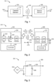
- Fig. 1 is a functional block diagram of a wireless power transfer system 100, in accordance with an illustrative embodiment.
- Input power 102 may be provided to a transmitter 104 from a power source (not shown in this figure) to generate a wireless (e.g., magnetic or electromagnetic) field 105 for performing energy transfer.
- a receiver 108 may couple to the wireless field 105 and generate output power 110 for storing or consumption by a device (not shown in this figure) coupled to the output power 110.
- the transmitter 104 and the receiver 108 may be separated by a distance 112.
- the transmitter 104 may include a power transmitting element 114 for transmitting/coupling energy to the receiver 108.
- the receiver 108 may include a power receiving element 118 for receiving or capturing/coupling energy transmitted from the transmitter 104.
- the transmitter 104 and the receiver 108 may be configured according to a mutual resonant relationship.
- the resonant frequency of the receiver 108 and the resonant frequency of the transmitter 104 are substantially the same or very close, transmission losses between the transmitter 104 and the receiver 108 are reduced.
- wireless power transfer may be provided over larger distances.
- Resonant inductive coupling techniques may thus allow for improved efficiency and power transfer over various distances and with a variety of inductive power transmitting and receiving element configurations.
- the wireless field 105 may correspond to the "near field" of the transmitter 104.
- the near-field may correspond to a region in which there are strong reactive fields resulting from the currents and charges in the power transmitting element 114 that minimally radiate power away from the power transmitting element 114.
- the near-field may correspond to a region that is within about one wavelength (or a fraction thereof) of the power transmitting element 114.
- efficient energy transfer may occur by coupling a large portion of the energy in the wireless field 105 to the power receiving element 118 rather than propagating most of the energy in an electromagnetic wave to the far field.
- the transmitter 104 may output a time varying magnetic (or electromagnetic) field 105 with a frequency corresponding to the resonant frequency of the power transmitting element 114.
- the time varying magnetic (or electromagnetic) field may induce a current in the power receiving element 118.
- the power receiving element 118 is configured as a resonant circuit to resonate at the frequency of the power transmitting element 114, energy may be efficiently transferred.
- An alternating current (AC) signal induced in the power receiving element 118 may be rectified to produce a direct current (DC) signal that may be provided to charge or to power a load.
- AC alternating current
- DC direct current
- Fig. 2 is a functional block diagram of a wireless power transfer system 200, in accordance with another illustrative embodiment.
- the system 200 may include a transmitter 204 and a receiver 208.
- the transmitter 204 (also referred to herein as power transfer unit, PTU) may include transmit circuitry 206 that may include an oscillator 222, a driver circuit 224, and a front-end circuit 226.
- the oscillator 222 may be configured to generate an oscillator signal at a desired frequency that may adjust in response to a frequency control signal 223.
- the oscillator 222 may provide the oscillator signal to the driver circuit 224.
- the driver circuit 224 may be configured to drive the power transmitting element 214 at, for example, a resonant frequency of the power transmitting element 214 based on an input voltage signal (VD) 225.
- the driver circuit 224 may be a switching amplifier configured to receive a square wave from the oscillator 222 and output a sine wave.
- the front-end circuit 226 may include a filter circuit configured to filter out harmonics or other unwanted frequencies.
- the front-end circuit 226 may include a matching circuit configured to match the impedance of the transmitter 204 to the impedance of the power transmitting element 214.
- the front-end circuit 226 may include a tuning circuit to create a resonant circuit with the power transmitting element 214. As a result of driving the power transmitting element 214, the power transmitting element 214 may generate a wireless field 205 to wirelessly output power at a level sufficient for charging a battery 236, or otherwise powering a load.
- the transmitter 204 may further include a controller 240 operably coupled to the transmit circuitry 206 and configured to control one or more aspects of the transmit circuitry 206, or accomplish other operations relevant to managing the transfer of power.
- the controller 240 may be a micro-controller or a processor.
- the controller 240 may be implemented as an application-specific integrated circuit (ASIC).
- ASIC application-specific integrated circuit
- the controller 240 may be operably connected, directly or indirectly, to each component of the transmit circuitry 206.
- the controller 240 may be further configured to receive information from each of the components of the transmit circuitry 206 and perform calculations based on the received information.
- the controller 240 may be configured to generate control signals (e.g., signal 223) for each of the components that may adjust the operation of that component.
- the controller 240 may be configured to adjust or manage the power transfer based on a result of the operations performed by it.
- the transmitter 204 may further include a memory (not shown) configured to store data, for example, such as instructions for causing the controller 240 to perform particular functions, such as those related to management of wireless power transfer.
- the receiver 208 may include receive circuitry 210 that may include a front-end circuit 232 and a rectifier circuit 234.
- the front-end circuit 232 may include matching circuitry configured to match the impedance of the receive circuitry 210 to the impedance of the power receiving element 218.
- the front-end circuit 232 may further include a tuning circuit to create a resonant circuit with the power receiving element 218.
- the rectifier circuit 234 may generate a DC power output from an AC power input to charge the battery 236, as shown in Fig. 2 .
- the receiver 208 and the transmitter 204 may additionally communicate on a separate communication channel 219 (e.g., Bluetooth, Zigbee, cellular, etc.).
- the receiver 208 and the transmitter 204 may alternatively communicate via in-band signaling using characteristics of the wireless field 205.
- the receiver 208 may be configured to determine whether an amount of power transmitted by the transmitter 204 and received by the receiver 208 is appropriate for charging the battery 236.
- the transmitter 204 may be configured to generate a predominantly non-radiative field with a direct field coupling coefficient (k) for providing energy transfer.
- Receiver 208 may directly couple to the wireless field 205 and may generate an output power for storing or consumption by a battery (or load) 236 coupled to the output or receive circuitry 210.
- the receiver 208 may further include a controller 250 configured similarly to the transmit controller 240 as described above for managing one or more aspects of the wireless power receiver 208.
- the receiver 208 may further include a memory (not shown) configured to store data, for example, such as instructions for causing the controller 250 to perform particular functions, such as those related to management of wireless power transfer.
- transmitter 204 and receiver 208 may be separated by a distance and may be configured according to a mutual resonant relationship to minimize transmission losses between the transmitter 204 and the receiver 208.
- Fig. 3 is a schematic diagram of a portion of the transmit circuitry 206 or the receive circuitry 210 of Fig. 2 , in accordance with illustrative embodiments.
- transmit or receive circuitry 350 may include a power transmitting or receiving element 352 and a tuning circuit 360.
- the power transmitting or receiving element 352 may also be referred to or be configured as an antenna or a "loop" antenna.
- the term “antenna” generally refers to a component that may wirelessly output or receive energy for coupling to another antenna.
- the power transmitting or receiving element 352 may also be referred to herein or be configured as a "magnetic" antenna, or an induction coil, a resonator, or a portion of a resonator.
- the power transmitting or receiving element 352 may also be referred to as a coil or resonator of a type that is configured to wirelessly output or receive power.
- the power transmitting or receiving element 352 is an example of a "power transfer component" of a type that is configured to wirelessly output and/or receive power.
- the power transmitting or receiving element 352 may include an air core or a physical core such as a ferrite core (not shown in this figure).
- the resonant frequency of the power transmitting or receiving element 352 may be based on the inductance and capacitance.
- Inductance may be simply the inductance created by a coil and/or other inductor forming the power transmitting or receiving element 352.
- Capacitance e.g., a capacitor
- the tuning circuit 360 may comprise a capacitor 354 and a capacitor 356, which may be added to the transmit and/or receive circuitry 350 to create a resonant circuit.
- the tuning circuit 360 may include other components to form a resonant circuit with the power transmitting or receiving element 352.
- the tuning circuit 360 may include a capacitor (not shown) placed in parallel between the two terminals of the circuitry 350. Still other designs are possible.
- the tuning circuit in the front-end circuit 226 may have the same design (e.g., 360) as the tuning circuit in front-end circuit 232. In other embodiments, the front-end circuit 226 may use a tuning circuit design different than in the front-end circuit 232.
- the signal 358 For power transmitting elements, the signal 358, with a frequency that substantially corresponds to the resonant frequency of the power transmitting or receiving element 352, may be an input to the power transmitting or receiving element 352.
- the signal 358 For power receiving elements, the signal 358, with a frequency that substantially corresponds to the resonant frequency of the power transmitting or receiving element 352, may be an output from the power transmitting or receiving element 352.
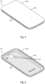
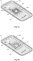
- Fig. 4 shows an electronic device 40, such as a smartphone for example. It will be understood, however, in other embodiments the electronic device 40 may be any portable electronic device such as a laptop, a computer tablet, and so on.
- the electronic device 40 may include means for enclosing the electronic components (not shown) that comprise the electronic device 40; for example, enclosure 400.
- the enclosure 400 may include a casing 402.
- the enclosure 400 may further include a transparent display cover 404, for example, such as in a smartphone or other computing device having a display.
- the casing 402 may house the electronic components of the electronic device 40.
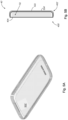
- Fig. 5 shows the casing 402 portion of the enclosure 400 with the display cover 404 removed and electronic components of the electronic device 40 taken out of the casing 402.
- the casing 402 may be entirely metal.
- the casing 400 may comprise at least a metal back cover portion 502 (metal back cover) supported by a frame portion 504.
- the frame portion 504 may comprise a non-metallic material, or a combination of metallic and non-metallic materials.
- the metal back cover 502 may have one or more openings 512 formed through the material that comprises the metal back cover 502.
- the openings 512 may be to expose the lens and flash unit of a camera (not shown) of the electronic device 40.
- the metal back cover 502 may otherwise be a continuous, uninterrupted, unbroken surface, as shown in Fig. 5 for example.
- the casing 402 may be configured to allow for wireless transfer of power to the electronic components (not shown) of the electronic device 40. This aspect of the present disclosure is discussed below.
- the electronic device 40 may not require openings on the back side of the device; for example, a computer tablet may have only a front-facing camera. Accordingly, in some embodiments the electronic device 40 may employ a metal back cover 502' that has no openings formed through the material.
- the metal back cover 502' may have a solid, unbroken, uninterrupted, continuous surface with no openings formed through it, such as shown in Fig. 5A .
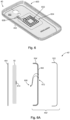
- Fig. 5B shows an embodiment of an electronic device 40' in accordance with some embodiments of the present disclosure.
- the electronic device 40' may include means for enclosing electronic components 52 that comprise the electronic device 40'; for example, enclosure 400'.
- the enclosure 400' may include a casing 402' to house the electronic components 52.
- the casing 402' may include a non-conductive shell (support substrate) 504' and a thin metal layer 522.
- the thin metal layer 522 formed on the support substrate 504' may serve as the metal back cover 502 ( Fig. 5 ) which has openings for a camera lens and such.
- the thin metal layer 522 may serve as the metal back cover 502' ( Fig. 5A ) which has no openings.
- the support substrate 504' may serve to provide mechanical stiffness and other structural support for the electronic device 40'.
- the support substrate 504' may comprise any electrically non-conductive material.
- the support substrate 504' may be non-ferromagnetic as well. Suitable materials may be lightweight, have strong mechanical properties, and have good heat dissipation performance to dissipate heat generated by the electronic components 52.
- a carbon-fiber compound may be used. It will be appreciated, however, that in other embodiments other materials may be used such as carbon nanotube materials, ceramics based materials, fiberglass, and the like.
- the casing 402' may be configured for wireless transfer of power to the electronic components 52 of the electronic device 40'.
- the thin metal layer 522 may be made from any suitable electrically conductive material, such as for example, aluminum, magnesium, carbon steel, stainless steel, other metallic alloys, and the like.
- the thin metal layer 522 may have a thickness less than 0.1mm in order to facilitate wireless power transfer. In a particular embodiment, for example, the thickness of thin metal layer 522 may be 0.7 mils (approximately 0.018mm) or less.
- the thin metal layer 522 may be formed as part separate from the support substrate 504' and then attached to the support substrate 504'. In other embodiments, the thin metal layer 504' may be deposited onto the support substrate 504', for example, using a suitable deposition method.
- the thin metal layer 522 may serve a dual purpose.
- the use of a metallic material for the back cover of the electronic device 40' allows for the incorporation of an aesthetic design element to the electronic device 40'.
- the task of housing the electronic components 52 and providing structural support for the electronic device 40' is provided by the support substrate 504' rather than the thin metal layer 522. This allows the thin metal layer 522 to be configured for the wireless transfer of power to the electronic device 40'. This aspect of the present disclosure is discussed in more detail below.
- the casing 402 may be configured to allow for wireless transfer of power to the electronic components (not shown) of the electronic device 40.
- the casing 402 may include an electrically conductive power receiving element 602 disposed on the interior surface of the metal back cover 502 of the casing 402. More particularly, the power receiving element 602 may be disposed in a given area 604 of the metal back cover 502 that is defined by a solid, unbroken, uninterrupted, continuous surface portion of the material used for the metal back cover 502.
- the power receiving element 602 may comprise a conductive trace formed on a flexible printed circuit board (PCB), for example, by printing, etching, photolithography, etc.
- the power receiving element 602 may be formed in the shape of a coil having any number of turns. Fig. 6 , for example, shows that power receiving element 602 comprises three turns. In some embodiments, the power receiving element 602 may have additional turns.
- the power receiving element 602 may be affixed directly to the interior surface of metal back cover 502, for example, using an adhesive, epoxy material, or other suitable affixing means.
- the power receiving element 602 may include or otherwise be connected to terminals 606 to provide power to electronic components (not shown) of the electronic device 40.
- the terminals 606 may be connected to a rectifier circuit (not shown) to produce a DC voltage that can be provided to the electronic components; for example, a rechargeable battery, a power management circuit, and so on.
- the casing 402' shown in Fig. 5B may likewise include an electrically conductive power receiving element 602.
- the power receiving element 602 may be disposed on the support substrate 504' Fig. 6A , for example, shows an exploded view of electronic device 40', illustrating some additional details in accordance with the present disclosure.
- a recessed portion 612 may be formed in the outwardly facing surface of the support substrate 504' to hold the power receiving element 602.
- the recessed portion 612 may be provided so that the thin metal layer 522 can be formed (e.g., as an inlay) atop the power receiving element 602 without any bumps on the surface of thin metal layer 522.
- the power receiving element 602 may be formed directly atop the surface of the support substrate 504' without a recessed portion; for example, so that an outline of some or all of power receiving element 602 in the design can be incorporated in the design of the backside of the casing 402'.
- the power receiving element 602 may include terminals 606 for connection to a rectifier circuit 614 in the electronic components 52 of the electronic device 40'.
- Fig. 6B illustrates an example of an embodiment in which the power receiving element 602 may be arranged on the inwardly facing surface of the support substrate 504'. The figure shows the power receiving element 602 disposed on the inwardly facing surface of support substrate 504', but in other embodiments the power receiving element 602 may be arranged in a recess similar to the arrangement shown in Fig. 6A .
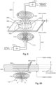
- wireless power transfer may include placing the electronic device 40, 40' in proximity to a charging surface (charging pad, etc.) 702 of a wireless power transmitting device 70.
- the charging surface 702 may include a transmit coil 712.
- the transmit coil 712 may be energized, for example, by providing an AC excitation current to the transmit coil 712.
- the transmit coil 712 may generate a magnetic field 714.
- the externally generated magnetic field 714 may couple to the power receiving element (602, Fig. 6 ) in the electronic device 40, 40'.
- the AC excitation current may operate any suitable frequency.
- the AC excitation current may operate at frequencies according to any of the various standards for wireless power transfer.
- the AirFuel/A4WP (Alliance for Wireless Power) wireless power transfer standard specifies an operating frequency of 6.87MHz
- the WPC wireless power standard developed by the Wireless Power Consortium (WPC), specifies frequencies in the range of 100 - 300KHz.
- Fig. 8 shows additional detail in the area 604 of the metal back cover 502 of the casing (402, Fig. 6 ).
- the casing 402 may include means for inducing eddy currents.
- the externally generated magnetic field 714 may induce eddy currents in the metal back cover 502.
- the eddy currents may circulate in planes perpendicular to the magnetic flux of the externally generated magnetic field 714.
- Fig. 8 shows eddy currents 802, 804 only in the area 604 of the metal back cover 502. It will be understood by persons of ordinary skill, however, that eddy currents are not necessarily restricted to the area 604.
- Eddy currents generally concentrate near the exterior surface of the metal back cover 502 surface adjacent to the transmit coil 712, due to the skin effect.
- the density of the eddy currents decreases (decays) with distance from the exterior surface of the metal back cover 502 toward the interior surface of the metal back cover 502. Accordingly, the density of eddy currents 802 at the exterior surface of the metal back cover 502 is greater than the density of eddy currents 804 at the interior surface of the metal back cover 502.
- the depth of penetration (“skin depth”) of the eddy currents into the metal back cover 502 varies with the frequency of the power used (e.g., AC excitation current) to excite the transmit coil 712 and the material that comprises the metal back cover 502.
- the excitation frequency of the power used to excite the transmit coil 712 may be in the 10's of KHz to 100's of KHz; for example, the WPC standard specifies frequencies in the range 100 - 300KHz.
- the transmit coil 712 may be connected to a tuning circuit 812 to define a resonant circuit 822.
- the excitation frequency may be substantially equal to a resonant frequency of the resonant circuit 822.
- the tuning circuit 812 may be any suitable combination of reactive elements (e.g., a capacitor network).
- the power receiving element 602 may be connected to a tuning circuit 814 to define a resonant circuit 824 that has a resonant frequency substantially equal to the excitation frequency of the power used to excite the transmit coil 712.
- the tuning circuit 814 may be any suitable combination of reactive elements, such as a capacitor network for example.
- the tuning circuits 812, 814 may use the circuit design of tuning circuit 360 shown in Fig. 3 . It will be understood that in various embodiments, the tuning circuits 812, 814 may employ any suitable circuit design.
- a magnetic field 806 can be generated in the metal back cover 502 that emanates from the metal back cover 502.
- means may be provided to couple to the magnetic field 806 generated by the eddy currents 802, 804.
- portions of the magnetic field 806 that emanate from interior surface of area 604 in the metal back cover 502 may couple to the power receiving element 602 of the electronic device 40 ( Fig. 6 ). This can induce a flow of current in the power receiving element 602, which can be rectified and provided to electronic components (not shown) of the electronic device 40.
- the material for metal back cover 502 may include metals such as copper, aluminum, magnesium, carbon steel, titanium, stainless steel, and the like.
- the metal back cover 502 may comprise a combination (e.g., a composite of metals, an alloy of metals, etc.) of two or more of copper, aluminum, magnesium, carbon steel, titanium, stainless steel.
- other suitable metals may be used, individually or in combination. The use of these materials allow for the metal back cover 502 to be sufficiently thin to allow for a skin depth that allows sufficient eddy currents to form at the interior surface of the metal back cover 502 to generate a magnetic field for wireless power transfer.
- the thickness t 1 of the material may be less the 1.0 mm. In other embodiments, the thickness t 1 may be 0.5 mm to 0.7 mm. These thickness values are merely illustrative, and the thickness t 1 can be other values in other embodiments.
- the eddy currents can remain concentrated substantially to the exterior surface of the metal back cover 502 due to the skin effect, while eddy currents at the interior surface of the metal back cover 502 can be attenuated as illustrated by the graph in Fig. 8A . Accordingly, the magnetic field induced by the eddy currents at the interior surface of the metal back cover 502 may not couple sufficient power to the power receiving element 602.
- eddy currents are less attenuated across the entire metal back cover 502 as illustrated by the graph in Fig. 8B .
- the eddy currents on the interior surface of the metal back cover 502 are therefore higher at a lower excitation frequency than at a higher excitation frequency, and thus can induce a stronger magnetic field from the interior surface to provide sufficiently strong coupling to the power receiving element 602.
- Fig. 8C illustrates operation when the metal back cover (e.g., 502, Fig. 5 , 502', Fig. 5A ) comprises a thin metal layer 522 ( Fig. 5B ).
- the thin metal layer 522 may have a thickness of about 0.01mm or less, and in some embodiments may be suitable for wireless power transfer at low excitation frequencies; e.g., 300KHz or less.
- the externally generated magnetic field 714 may penetrate the thin metal layer 522, as depicted in Fig. 8C for example, and couple to the power receiving element 602.
- the wireless standards and excitation frequencies disclosed herein are merely examples to illustrate this aspect of the present disclosure in the context of known wireless charging systems.
- the support substrate 504' can allow for the thickness of thin metal layer 522 to be adapted for a variety of different implementations to work with a variety of different frequency ranges, and is not necessarily limited to any particular frequency range.
- a layer of ferrite material 902 may be positioned between the power receiving element 602 and the metal back cover 502.
- the ferrite material 902 may serve to improve the mutual coupling of the generated magnetic field (806, Fig. 8 ) and the power receiving element 602.
- the ferrite material 902 may enhance penetration of the externally generated magnetic field (714, Fig. 8 ) through the metal back cover 502, thus enhancing the induction of eddy currents in the metal back cover 502.
- a layer of ferrite material 904 maybe provided on top of the power receiving element 602 so that the power receiving element 602 is positioned between the ferrite material 904 and the metal back cover 502.
- the ferrite material 904 may serve to enhance the coupling of the magnetic field 806 generated in the metal back cover 502 to the power receiving element 602 as explained above.
- the ferrite material 904 may also serve to shield electronic components (not shown) comprising the electronic device 40 from the magnetic field 806.
- the power receiving element 602 may be sandwiched between a first layer and a second layer of ferrite material.
- the ferrite material 902 may serve to channel the magnetic field 806 generated by the eddy currents such that flux is concentrated near the power receiving element 602.
- the power receiving element 602 may be disposed on the outwardly facing surface of the support structure 504', and a layer of ferrite material 912a may be provided between the power receiving element 602 and the thin metal layer 522 to enhance penetration of the externally generated magnetic field 714 through the thin metal layer 522 and improve mutual coupling between the externally generated magnetic field (714, Fig. 8C ) and the power receiving element 602.
- a layer of ferrite material 912b may be provided instead of or in addition to ferrite material 912a.
- the ferrite material 912b may be placed on the inside surface of the support structure 504'.
- the power receiving element 602 may be disposed on the inwardly facing surface of the support structure 504'.
- the layer of ferrite material 912b and support structure 504' may sandwich the power receiving element 602 to enhance penetration of the externally generated magnetic field 714 through the thin metal layer 522 and improve mutual coupling between the externally generated magnetic field (714, Fig. 8C ) and the power receiving element 602.
- the layer of ferrite material 912a may be provided instead of or in addition to ferrite material 912b.
- HFSS TM High Frequency Structure Simulator
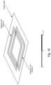
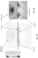
- Fig. 10 illustrates a setup for the simulation.
- the receive and transmit coils are identical.
- the receive coil e.g., power receiving element 602
- the transmit coil is shown to be below the metal plate.
- the metal plate is characterized as having a thickness of 1 mm and a conductivity of 11000 siemens/m.
- Figs. 11A and 11B illustrate a frequency sweep result for an electromagnetic simulation for the setup shown in Fig. 10 .
- the simulation frequencies vary from about 60 kHz to 7 MHz.
- Fig. 11A shows the sweep result from 60 kHz to 500 kHz.
- the plot shows mutual inductance M on the vertical scale and frequency in kHz on the horizontal scale.
- Fig. 11B shows the sweep result from about 10kHz to 7 MHz.
- the plot shows mutual inductance M on the vertical scale and frequency in MHz on the horizontal scale.
- Three regions (1,2, 3) are defined based on frequency ranges.
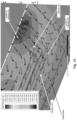
- the map simulation of Fig. 12 shows that current in the transmit coil flows in the opposite direction as current in the receive coil and eddy currents in the metal plate. The strength of the surrounding magnetic field is shown in gray scale.
- Figs. 11A , 13A and 13B for a given thickness of a metal plate (e.g. 1mm), we see that at a very low frequency (60kHz), M is positive because eddy currents on the metal plate are substantially uniformly strong and magnetic flux direction in the transmit coil is that same as the magnetic flux direction in the receive coil.
- the Fig. 13A shows the magnetic flux lines for very low frequency excitations. At low frequencies, the magnetic flux is additive.
- Fig. 13B shows a simulated heat map illustrating the field strength at different areas of the metal plate. The field strength is generally high on the side of the transmit coil and on the side of the receive coil, with an area of low field strength. The area of low field strength is due to the symmetry of the eddy current in that area of the metal plate.
- Figs. 11A , 14A and 14B at a low frequency (115kHz), mutual inductance M is negative because the eddy current is not uniform across the metal plate. This causes the induced magnetic flux to be directed in the opposite direction of the magnetic flux from the transmit coil.
- Fig. 14A shows the magnetic flux lines and Fig. 14B shows the corresponding magnitude of magnetic field strength. A weak area of magnetic field is observed around the center of the receive coil due to symmetry of the eddy current, similar to Fig. 13B .
- Figs. 11B , 15A and 15B at a relatively high frequency (6.78 MHz), the eddy current on the metal plate is very small throughout the metal plate ( Fig. 15A ) and M is accordingly almost zero.
- Fig. 15B shows the field strength to be low for much of area on the side of the receive coil.
Landscapes
- Engineering & Computer Science (AREA)
- Computer Networks & Wireless Communication (AREA)
- Power Engineering (AREA)
- Signal Processing (AREA)
- Charge And Discharge Circuits For Batteries Or The Like (AREA)
Applications Claiming Priority (2)
| Application Number | Priority Date | Filing Date | Title |
|---|---|---|---|
| US201562168483P | 2015-05-29 | 2015-05-29 | |
| PCT/US2016/034833 WO2016196372A1 (en) | 2015-05-29 | 2016-05-27 | Wireless power transfer using direct field penetration through a metal object |
Publications (2)
| Publication Number | Publication Date |
|---|---|
| EP3304690A1 EP3304690A1 (en) | 2018-04-11 |
| EP3304690B1 true EP3304690B1 (en) | 2025-06-18 |
Family
ID=57399030
Family Applications (1)
| Application Number | Title | Priority Date | Filing Date |
|---|---|---|---|
| EP16730122.5A Active EP3304690B1 (en) | 2015-05-29 | 2016-05-27 | Wireless power transfer using direct field penetration through a metal object |
Country Status (5)
| Country | Link |
|---|---|
| US (1) | US10333350B2 (enExample) |
| EP (1) | EP3304690B1 (enExample) |
| JP (1) | JP6605625B2 (enExample) |
| CN (1) | CN107690742B (enExample) |
| WO (1) | WO2016196372A1 (enExample) |
Families Citing this family (11)
| Publication number | Priority date | Publication date | Assignee | Title |
|---|---|---|---|---|
| KR102593172B1 (ko) * | 2016-10-05 | 2023-10-24 | 삼성전자 주식회사 | 루프 안테나를 갖는 전자 장치 |
| US10469119B2 (en) * | 2017-05-25 | 2019-11-05 | Spigen Korea Co., Ltd. | Magnetic mount for electronic devices |
| US12191902B2 (en) | 2017-05-25 | 2025-01-07 | Spigen Korea Co., Ltd. | Mobile electronic device cases for electromagnetic shielding |
| US12224788B2 (en) * | 2017-05-25 | 2025-02-11 | Spigen Korea Co., Ltd. | Magnetic auxiliary devices for mobile devices |
| CN108695993A (zh) * | 2018-05-29 | 2018-10-23 | 电子科技大学 | 一种基于陶瓷谐振器的多级无线功率传输系统 |
| JP2020096414A (ja) * | 2018-12-10 | 2020-06-18 | シャープ株式会社 | ケース |
| CN209434964U (zh) * | 2019-02-18 | 2019-09-24 | 邢益涛 | 一种具有卡环结构的无线充电发射装置 |
| US11502554B2 (en) | 2020-01-23 | 2022-11-15 | Wen Cai | Methods and apparatus for online foreign object detection in wireless charging systems |
| CN115038744B (zh) * | 2020-02-06 | 2024-07-09 | 东丽株式会社 | 碳纤维增强复合材料、层叠碳纤维复合材料、层叠复合材料、用于无线供电器的壳体和用于无线受电器的壳体 |
| WO2024030614A1 (en) * | 2022-08-05 | 2024-02-08 | Resonant Link, Inc. | High efficiency wireless power transfer to implantable devices |
| JP2024039913A (ja) * | 2022-09-12 | 2024-03-25 | トヨタ自動車株式会社 | 送電コイルユニット |
Citations (3)
| Publication number | Priority date | Publication date | Assignee | Title |
|---|---|---|---|---|
| TW201112569A (en) * | 2009-05-20 | 2011-04-01 | Koninkl Philips Electronics Nv | Electronic device having an inductive receiver coil with ultra-thin shielding layer and method |
| US20130285604A1 (en) * | 2011-01-18 | 2013-10-31 | Mojo Mobility, Inc. | Systems and methods for wireless power transfer |
| US20150077053A1 (en) * | 2013-09-13 | 2015-03-19 | Qualcomm Incorporated | Pickup coil design for tight spaces and asymmetrical coupling |
Family Cites Families (22)
| Publication number | Priority date | Publication date | Assignee | Title |
|---|---|---|---|---|
| US6265789B1 (en) * | 1997-11-20 | 2001-07-24 | Seiko Epson Corporation | Electronic apparatus |
| US7599743B2 (en) * | 2004-06-24 | 2009-10-06 | Ethicon Endo-Surgery, Inc. | Low frequency transcutaneous energy transfer to implanted medical device |
| KR101233421B1 (ko) * | 2004-09-09 | 2013-02-13 | 가부시키가이샤 한도오따이 에네루기 켄큐쇼 | 반도체 장치 |
| US20070217163A1 (en) | 2006-03-15 | 2007-09-20 | Wilson Greatbatch | Implantable medical electronic device with amorphous metallic alloy enclosure |
| US10115520B2 (en) * | 2011-01-18 | 2018-10-30 | Mojo Mobility, Inc. | Systems and method for wireless power transfer |
| US20120274148A1 (en) * | 2011-04-27 | 2012-11-01 | Samsung Electro-Mechanics Co., Ltd. | Contactless power transmission device and electronic device having the same |
| US9531195B2 (en) | 2011-04-29 | 2016-12-27 | Cyberonics, Inc. | Inductively rechargeable implantable device with reduced eddy currents |
| WO2013056021A1 (en) | 2011-10-13 | 2013-04-18 | Access Business Group International Llc | Composite metal surface |
| US9252611B2 (en) * | 2011-12-21 | 2016-02-02 | Amosense Co., Ltd. | Magnetic field shielding sheet for a wireless charger, method for manufacturing same, and receiving apparatus for a wireless charger using the sheet |
| US9743565B2 (en) | 2012-01-08 | 2017-08-22 | Access Business Group International Llc | Wireless power transfer through conductive materials |
| JP5890191B2 (ja) * | 2012-02-06 | 2016-03-22 | トヨタ自動車株式会社 | 送電装置、受電装置、および電力伝送システム |
| JP5942530B2 (ja) | 2012-03-28 | 2016-06-29 | カシオ計算機株式会社 | 非接触充電システム及び電子機器 |
| JP6112383B2 (ja) * | 2012-06-28 | 2017-04-12 | パナソニックIpマネジメント株式会社 | 携帯端末 |
| CN103918125B (zh) * | 2012-09-26 | 2017-03-08 | 株式会社村田制作所 | 天线装置及具备天线装置的电子设备 |
| KR101444552B1 (ko) * | 2012-12-21 | 2014-10-30 | 삼성전기주식회사 | 자성체 시트, 자성체 시트의 제조방법 및 자성체 시트를 포함하는 무접점 전력 충전 장치 |
| WO2014167881A1 (ja) * | 2013-04-08 | 2014-10-16 | 株式会社村田製作所 | 通信端末 |
| US10096903B2 (en) | 2013-04-12 | 2018-10-09 | Panasonic Intellectual Property Management Co., Ltd. | Antenna, antenna device and communication device |
| CN103346623A (zh) * | 2013-07-15 | 2013-10-09 | 曾超宁 | 低频透射式电力传输装置 |
| JP6171726B2 (ja) * | 2013-08-23 | 2017-08-02 | 株式会社Ihi | 非接触給電装置の製造方法 |
| EP3057114B1 (en) * | 2013-08-08 | 2018-09-19 | IHI Corporation | Resonator |
| US9461500B2 (en) | 2013-11-21 | 2016-10-04 | Htc Corporation | Wireless charging receiving device and wireless charging system using the same |
| JP2015149833A (ja) * | 2014-02-06 | 2015-08-20 | デクセリアルズ株式会社 | 電子機器 |
-
2016
- 2016-05-27 EP EP16730122.5A patent/EP3304690B1/en active Active
- 2016-05-27 JP JP2017560960A patent/JP6605625B2/ja active Active
- 2016-05-27 US US15/167,680 patent/US10333350B2/en active Active
- 2016-05-27 WO PCT/US2016/034833 patent/WO2016196372A1/en not_active Ceased
- 2016-05-27 CN CN201680030828.9A patent/CN107690742B/zh active Active
Patent Citations (4)
| Publication number | Priority date | Publication date | Assignee | Title |
|---|---|---|---|---|
| TW201112569A (en) * | 2009-05-20 | 2011-04-01 | Koninkl Philips Electronics Nv | Electronic device having an inductive receiver coil with ultra-thin shielding layer and method |
| US20130285604A1 (en) * | 2011-01-18 | 2013-10-31 | Mojo Mobility, Inc. | Systems and methods for wireless power transfer |
| US20150077053A1 (en) * | 2013-09-13 | 2015-03-19 | Qualcomm Incorporated | Pickup coil design for tight spaces and asymmetrical coupling |
| US10186912B2 (en) * | 2013-09-13 | 2019-01-22 | Qualcomm Incorporated | Pickup coil design for tight spaces and asymmetrical coupling |
Also Published As
| Publication number | Publication date |
|---|---|
| CN107690742A (zh) | 2018-02-13 |
| EP3304690A1 (en) | 2018-04-11 |
| US20160352151A1 (en) | 2016-12-01 |
| JP2018522514A (ja) | 2018-08-09 |
| JP6605625B2 (ja) | 2019-11-13 |
| US10333350B2 (en) | 2019-06-25 |
| CN107690742B (zh) | 2021-01-12 |
| WO2016196372A1 (en) | 2016-12-08 |
Similar Documents
| Publication | Publication Date | Title |
|---|---|---|
| EP3304690B1 (en) | Wireless power transfer using direct field penetration through a metal object | |
| JP6612863B2 (ja) | ワイヤレス電力伝達のためのセグメント化された導電性バックカバー | |
| CN115336136A (zh) | 用于无线功率传递的具有磁性继电器结构的附件 | |
| US10122182B2 (en) | Multi-turn coil on metal backplate | |
| KR20230005363A (ko) | 상이한 주파수들에서의 동시 무선 전력 전달을 이용하는 무선 충전 시스템 | |
| CN106662896A (zh) | 通过金属物体的无线功率传送 | |
| JP6696573B2 (ja) | 無線モジュール、rfidシステムおよびワイヤレス給電装置 | |
| EP3189576B1 (en) | Wireless charging of metal backed electronic devices | |
| US10312716B2 (en) | EMI filtering and wireless power transfer in an electronic device using a tuned metallic body | |
| US10361588B2 (en) | Coupled resonator in a metal back cover | |
| US20170063169A1 (en) | Receiver detuning compensation using transmitter ferrite | |
| JP2017005952A (ja) | 非接触電力送電装置、非接触電力受電装置、及び、非接触電力伝送システム | |
| BR112018015387B1 (pt) | Transferência de energia sem fio em um dispositivo eletrônico com um corpo metálico sintonizado | |
| JP2017163670A (ja) | 電子機器 |
Legal Events
| Date | Code | Title | Description |
|---|---|---|---|
| STAA | Information on the status of an ep patent application or granted ep patent |
Free format text: STATUS: THE INTERNATIONAL PUBLICATION HAS BEEN MADE |
|
| PUAI | Public reference made under article 153(3) epc to a published international application that has entered the european phase |
Free format text: ORIGINAL CODE: 0009012 |
|
| STAA | Information on the status of an ep patent application or granted ep patent |
Free format text: STATUS: REQUEST FOR EXAMINATION WAS MADE |
|
| 17P | Request for examination filed |
Effective date: 20171009 |
|
| AK | Designated contracting states |
Kind code of ref document: A1 Designated state(s): AL AT BE BG CH CY CZ DE DK EE ES FI FR GB GR HR HU IE IS IT LI LT LU LV MC MK MT NL NO PL PT RO RS SE SI SK SM TR |
|
| AX | Request for extension of the european patent |
Extension state: BA ME |
|
| DAV | Request for validation of the european patent (deleted) | ||
| DAX | Request for extension of the european patent (deleted) | ||
| STAA | Information on the status of an ep patent application or granted ep patent |
Free format text: STATUS: EXAMINATION IS IN PROGRESS |
|
| 17Q | First examination report despatched |
Effective date: 20190509 |
|
| GRAP | Despatch of communication of intention to grant a patent |
Free format text: ORIGINAL CODE: EPIDOSNIGR1 |
|
| STAA | Information on the status of an ep patent application or granted ep patent |
Free format text: STATUS: GRANT OF PATENT IS INTENDED |
|
| INTG | Intention to grant announced |
Effective date: 20250203 |
|
| GRAS | Grant fee paid |
Free format text: ORIGINAL CODE: EPIDOSNIGR3 |
|
| GRAA | (expected) grant |
Free format text: ORIGINAL CODE: 0009210 |
|
| STAA | Information on the status of an ep patent application or granted ep patent |
Free format text: STATUS: THE PATENT HAS BEEN GRANTED |
|
| AK | Designated contracting states |
Kind code of ref document: B1 Designated state(s): AL AT BE BG CH CY CZ DE DK EE ES FI FR GB GR HR HU IE IS IT LI LT LU LV MC MK MT NL NO PL PT RO RS SE SI SK SM TR |
|
| REG | Reference to a national code |
Ref country code: GB Ref legal event code: FG4D |
|
| REG | Reference to a national code |
Ref country code: CH Ref legal event code: EP |
|
| REG | Reference to a national code |
Ref country code: DE Ref legal event code: R096 Ref document number: 602016092585 Country of ref document: DE |
|
| REG | Reference to a national code |
Ref country code: CH Ref legal event code: EP |
|
| REG | Reference to a national code |
Ref country code: IE Ref legal event code: FG4D |
|
| PG25 | Lapsed in a contracting state [announced via postgrant information from national office to epo] |
Ref country code: FI Free format text: LAPSE BECAUSE OF FAILURE TO SUBMIT A TRANSLATION OF THE DESCRIPTION OR TO PAY THE FEE WITHIN THE PRESCRIBED TIME-LIMIT Effective date: 20250618 |
|
| REG | Reference to a national code |
Ref country code: LT Ref legal event code: MG9D |
|
| PG25 | Lapsed in a contracting state [announced via postgrant information from national office to epo] |
Ref country code: NO Free format text: LAPSE BECAUSE OF FAILURE TO SUBMIT A TRANSLATION OF THE DESCRIPTION OR TO PAY THE FEE WITHIN THE PRESCRIBED TIME-LIMIT Effective date: 20250918 Ref country code: GR Free format text: LAPSE BECAUSE OF FAILURE TO SUBMIT A TRANSLATION OF THE DESCRIPTION OR TO PAY THE FEE WITHIN THE PRESCRIBED TIME-LIMIT Effective date: 20250919 |
|
| PG25 | Lapsed in a contracting state [announced via postgrant information from national office to epo] |
Ref country code: BG Free format text: LAPSE BECAUSE OF FAILURE TO SUBMIT A TRANSLATION OF THE DESCRIPTION OR TO PAY THE FEE WITHIN THE PRESCRIBED TIME-LIMIT Effective date: 20250618 |
|
| PG25 | Lapsed in a contracting state [announced via postgrant information from national office to epo] |
Ref country code: HR Free format text: LAPSE BECAUSE OF FAILURE TO SUBMIT A TRANSLATION OF THE DESCRIPTION OR TO PAY THE FEE WITHIN THE PRESCRIBED TIME-LIMIT Effective date: 20250618 |
|
| PG25 | Lapsed in a contracting state [announced via postgrant information from national office to epo] |
Ref country code: RS Free format text: LAPSE BECAUSE OF FAILURE TO SUBMIT A TRANSLATION OF THE DESCRIPTION OR TO PAY THE FEE WITHIN THE PRESCRIBED TIME-LIMIT Effective date: 20250918 |
|
| REG | Reference to a national code |
Ref country code: NL Ref legal event code: MP Effective date: 20250618 |
|
| PG25 | Lapsed in a contracting state [announced via postgrant information from national office to epo] |
Ref country code: LV Free format text: LAPSE BECAUSE OF FAILURE TO SUBMIT A TRANSLATION OF THE DESCRIPTION OR TO PAY THE FEE WITHIN THE PRESCRIBED TIME-LIMIT Effective date: 20250618 |
|
| PG25 | Lapsed in a contracting state [announced via postgrant information from national office to epo] |
Ref country code: NL Free format text: LAPSE BECAUSE OF FAILURE TO SUBMIT A TRANSLATION OF THE DESCRIPTION OR TO PAY THE FEE WITHIN THE PRESCRIBED TIME-LIMIT Effective date: 20250618 |
|
| PG25 | Lapsed in a contracting state [announced via postgrant information from national office to epo] |
Ref country code: PT Free format text: LAPSE BECAUSE OF FAILURE TO SUBMIT A TRANSLATION OF THE DESCRIPTION OR TO PAY THE FEE WITHIN THE PRESCRIBED TIME-LIMIT Effective date: 20251020 |