EP3299772A1 - Displacement sensor - Google Patents
Displacement sensor Download PDFInfo
- Publication number
- EP3299772A1 EP3299772A1 EP17190292.7A EP17190292A EP3299772A1 EP 3299772 A1 EP3299772 A1 EP 3299772A1 EP 17190292 A EP17190292 A EP 17190292A EP 3299772 A1 EP3299772 A1 EP 3299772A1
- Authority
- EP
- European Patent Office
- Prior art keywords
- detection
- pair
- detection units
- units
- disposed
- Prior art date
- Legal status (The legal status is an assumption and is not a legal conclusion. Google has not performed a legal analysis and makes no representation as to the accuracy of the status listed.)
- Granted
Links
Images
Classifications
-
- G—PHYSICS
- G01—MEASURING; TESTING
- G01D—MEASURING NOT SPECIALLY ADAPTED FOR A SPECIFIC VARIABLE; ARRANGEMENTS FOR MEASURING TWO OR MORE VARIABLES NOT COVERED IN A SINGLE OTHER SUBCLASS; TARIFF METERING APPARATUS; MEASURING OR TESTING NOT OTHERWISE PROVIDED FOR
- G01D5/00—Mechanical means for transferring the output of a sensing member; Means for converting the output of a sensing member to another variable where the form or nature of the sensing member does not constrain the means for converting; Transducers not specially adapted for a specific variable
- G01D5/12—Mechanical means for transferring the output of a sensing member; Means for converting the output of a sensing member to another variable where the form or nature of the sensing member does not constrain the means for converting; Transducers not specially adapted for a specific variable using electric or magnetic means
- G01D5/14—Mechanical means for transferring the output of a sensing member; Means for converting the output of a sensing member to another variable where the form or nature of the sensing member does not constrain the means for converting; Transducers not specially adapted for a specific variable using electric or magnetic means influencing the magnitude of a current or voltage
- G01D5/142—Mechanical means for transferring the output of a sensing member; Means for converting the output of a sensing member to another variable where the form or nature of the sensing member does not constrain the means for converting; Transducers not specially adapted for a specific variable using electric or magnetic means influencing the magnitude of a current or voltage using Hall-effect devices
-
- G—PHYSICS
- G01—MEASURING; TESTING
- G01D—MEASURING NOT SPECIALLY ADAPTED FOR A SPECIFIC VARIABLE; ARRANGEMENTS FOR MEASURING TWO OR MORE VARIABLES NOT COVERED IN A SINGLE OTHER SUBCLASS; TARIFF METERING APPARATUS; MEASURING OR TESTING NOT OTHERWISE PROVIDED FOR
- G01D11/00—Component parts of measuring arrangements not specially adapted for a specific variable
- G01D11/30—Supports specially adapted for an instrument; Supports specially adapted for a set of instruments
-
- G—PHYSICS
- G01—MEASURING; TESTING
- G01D—MEASURING NOT SPECIALLY ADAPTED FOR A SPECIFIC VARIABLE; ARRANGEMENTS FOR MEASURING TWO OR MORE VARIABLES NOT COVERED IN A SINGLE OTHER SUBCLASS; TARIFF METERING APPARATUS; MEASURING OR TESTING NOT OTHERWISE PROVIDED FOR
- G01D5/00—Mechanical means for transferring the output of a sensing member; Means for converting the output of a sensing member to another variable where the form or nature of the sensing member does not constrain the means for converting; Transducers not specially adapted for a specific variable
- G01D5/12—Mechanical means for transferring the output of a sensing member; Means for converting the output of a sensing member to another variable where the form or nature of the sensing member does not constrain the means for converting; Transducers not specially adapted for a specific variable using electric or magnetic means
- G01D5/244—Mechanical means for transferring the output of a sensing member; Means for converting the output of a sensing member to another variable where the form or nature of the sensing member does not constrain the means for converting; Transducers not specially adapted for a specific variable using electric or magnetic means influencing characteristics of pulses or pulse trains; generating pulses or pulse trains
- G01D5/24471—Error correction
- G01D5/24485—Error correction using other sensors
-
- G—PHYSICS
- G01—MEASURING; TESTING
- G01R—MEASURING ELECTRIC VARIABLES; MEASURING MAGNETIC VARIABLES
- G01R33/00—Arrangements or instruments for measuring magnetic variables
- G01R33/0005—Geometrical arrangement of magnetic sensor elements; Apparatus combining different magnetic sensor types
-
- H—ELECTRICITY
- H10—SEMICONDUCTOR DEVICES; ELECTRIC SOLID-STATE DEVICES NOT OTHERWISE PROVIDED FOR
- H10W—GENERIC PACKAGES, INTERCONNECTIONS, CONNECTORS OR OTHER CONSTRUCTIONAL DETAILS OF DEVICES COVERED BY CLASS H10
- H10W72/00—Interconnections or connectors in packages
- H10W72/851—Dispositions of multiple connectors or interconnections
- H10W72/853—On the same surface
- H10W72/865—Die-attach connectors and bond wires
-
- H—ELECTRICITY
- H10—SEMICONDUCTOR DEVICES; ELECTRIC SOLID-STATE DEVICES NOT OTHERWISE PROVIDED FOR
- H10W—GENERIC PACKAGES, INTERCONNECTIONS, CONNECTORS OR OTHER CONSTRUCTIONAL DETAILS OF DEVICES COVERED BY CLASS H10
- H10W72/00—Interconnections or connectors in packages
- H10W72/851—Dispositions of multiple connectors or interconnections
- H10W72/874—On different surfaces
- H10W72/884—Die-attach connectors and bond wires
-
- H—ELECTRICITY
- H10—SEMICONDUCTOR DEVICES; ELECTRIC SOLID-STATE DEVICES NOT OTHERWISE PROVIDED FOR
- H10W—GENERIC PACKAGES, INTERCONNECTIONS, CONNECTORS OR OTHER CONSTRUCTIONAL DETAILS OF DEVICES COVERED BY CLASS H10
- H10W90/00—Package configurations
- H10W90/701—Package configurations characterised by the relative positions of pads or connectors relative to package parts
- H10W90/731—Package configurations characterised by the relative positions of pads or connectors relative to package parts of die-attach connectors
- H10W90/732—Package configurations characterised by the relative positions of pads or connectors relative to package parts of die-attach connectors between stacked chips
-
- H—ELECTRICITY
- H10—SEMICONDUCTOR DEVICES; ELECTRIC SOLID-STATE DEVICES NOT OTHERWISE PROVIDED FOR
- H10W—GENERIC PACKAGES, INTERCONNECTIONS, CONNECTORS OR OTHER CONSTRUCTIONAL DETAILS OF DEVICES COVERED BY CLASS H10
- H10W90/00—Package configurations
- H10W90/701—Package configurations characterised by the relative positions of pads or connectors relative to package parts
- H10W90/731—Package configurations characterised by the relative positions of pads or connectors relative to package parts of die-attach connectors
- H10W90/736—Package configurations characterised by the relative positions of pads or connectors relative to package parts of die-attach connectors between a chip and a stacked lead frame, conducting package substrate or heat sink
-
- H—ELECTRICITY
- H10—SEMICONDUCTOR DEVICES; ELECTRIC SOLID-STATE DEVICES NOT OTHERWISE PROVIDED FOR
- H10W—GENERIC PACKAGES, INTERCONNECTIONS, CONNECTORS OR OTHER CONSTRUCTIONAL DETAILS OF DEVICES COVERED BY CLASS H10
- H10W90/00—Package configurations
- H10W90/701—Package configurations characterised by the relative positions of pads or connectors relative to package parts
- H10W90/751—Package configurations characterised by the relative positions of pads or connectors relative to package parts of bond wires
- H10W90/756—Package configurations characterised by the relative positions of pads or connectors relative to package parts of bond wires between a chip and a stacked lead frame, conducting package substrate or heat sink
Definitions
- This invention relates to a displacement sensor that detects the amount of displacement of a detection target.
- This type of displacement sensor may be configured by using, for example, semiconductor (for example, JP 6-104380 A , JP 8-213541 A , and JP 2000-156464 A ).
- a semiconductor integrated circuit device described in JP 6-104380 A includes a first semiconductor chip provided on a lower surface of an inner lead through a first insulating layer, and a second semiconductor chip provided on an upper surface of the inner lead through a second insulating layer.
- Each of the first semiconductor chip and the second semiconductor chip is provided with a bonding pad on each of the surfaces facing the same direction, and is wire-bonded to predetermined portions on the upper surface of the inner lead.
- bump electrodes having the same function as each other in a first semiconductor chip and a second semiconductor chip are disposed to face each other and are connected to the same lead.
- a first semiconductor chip and a second semiconductor chip are directed to surfaces (back surfaces) opposite to respective circuit formation surfaces (front surfaces) and are bonded to be fixed in a stacked state in which positions are shifted in a direction orthogonal to a disposition direction of external electrodes provided on the circuit formation surfaces.
- a vehicle, an airplane or the like may be provided with a plurality of circuits (for example, a detection unit) having the same function from the viewpoint of safety.
- circuits for example, a detection unit
- wire bonding is performed by using an upper surface of an inner lead, and thereby, it is necessary to shift a position of each chip, and there is a possibility that sensing accuracies of each of the circuits are significantly different from each other in use in which a positional relationship between a sensing point such as a magnetic sensor and a detection target is important.
- a first semiconductor chip and a second semiconductor chip need to be disposed to interpose an inner lead therebetween, and thereby, more chips cannot be stacked, and thicknesses of components increase by thicknesses of bump electrodes which connect the inner lead, the first semiconductor chip, and the second semiconductor chip to each other.
- wire bonding is performed by using surfaces of a first semiconductor chip and a second semiconductor chip, which do not face each other, and thereby, thicknesses thereof increase by a height of a wire.
- one object of the present invention is to provide a displacement sensor which is capable of reducing a difference between sensing accuracies of each of detection units even in a case where a plurality of the detection units having the same function is provided.
- a feature of a displacement sensor resides in that the displacement sensor includes a pair of first detection units that are configured to detect an amount of displacement of a same detection target, and are disposed such that detection surfaces for detecting the amount of displacement face each other; a pair of second detection units that are configured to detect an amount of displacement of the detection target which is the same as the detection target of the pair of first detection units, and are disposed such that detection surfaces for detecting the amount of displacement face each other; and a lead frame that includes a main frame having one surface on which the pair of first detection units are disposed and the other surface on which the pair of second detection units are disposed, and a sub frame which is wire-bonded to electrodes which are provided on each detection surface of the pair of first detection units and the pair of second detection units.
- detection surfaces of a pair of first detection units are disposed to face each other, and thereby, the pair of first detection units can be closer to each other in a stacked direction of the pair of first detection units.
- detection surfaces of a pair of second detection units face each other, and thereby, the pair of second detection units can be closer to each other in a stacked direction of the pair of second detection units.
- a main frame is disposed so as to be interposed between the pair of first detection units and the pair of second detection units, and thereby, the pair of first detection units and the pair of second detection units can be closer to each other.
- each electrode of the pair of first detection units can be disposed so as to face a central side of the pair of first detection units in the stacked direction
- each electrode of the pair of second detection units can be disposed so as to face a central side of the pair of second detection units in the stacked direction, and thereby, it is possible to obtain a margin for a height by a thickness of at least one of the first detection units or the second detection units, when wire bonding is performed. Therefore, it is possible to prevent a height of the entire package from becoming too high when the displacement sensor is contained in the package.
- the pair of first detection units and the pair of second detection units are disposed to face each other through the main frame.
- a displacement sensor described here is provided with a plurality of detection units having the same function and is configured such that a difference between detection results each of the detection units is small.
- a displacement sensor 1 of the present embodiment will be described by using an example of a case where the displacement sensor is applied to a magnetic sensor that detects magnetic flux density.
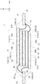
- the figure is a side sectional view of the displacement sensor 1 of the present embodiment. As illustrated in the figure, the displacement sensor 1 is configured to include first detection units 10, second detection units 20, and a lead frame 30.
- the first detection units 10 are configured with a pair of first detection units 10A and 10B.
- the first detection units 10A and 10B detect the amount of displacement of the same detection target, and detection surfaces 11 for detecting the amount of displacement are disposed to face each other.
- “the detection units 10A and 10B detect the amount of displacement of the same detection target” means that both the first detection unit 10A and the first detection unit 10B detect the amount of rotation or a rotation angle (hereinafter, referred to as "the amount of rotation or the like") of a magnet attached to a rotation body as a detection target.
- the first detection units 10A and 10B can be configured by using, for example, Hall elements.
- the detection surface 11 for detecting the amount of displacement corresponds to a detection surface 11A in the first detection unit 10A and corresponds to a detection surface 11B in the first detection unit 10B.
- the detection surfaces 11A and 11B respectively correspond to detection surfaces of the Hall elements.
- the first detection unit 10A and the first detection unit 10B are disposed through an adhesive 50 such that the detection surface 11A of the first detection unit 10A and the detection surface 11B of the first detection unit 10B face each other.
- mutual detection points can be closer (that is, a distance in the Z-axis direction between the detection point of the first detection unit 10A and the detection point of the first detection unit 10B can be shortened), and thus, it is possible to reduce a difference between detection results of each of the first detection units 10A and 10B.
- the second detection units 20 are configured with a pair of second detection units 20A and 20B.
- the second detection units 20A and 20B detect the amount of displacement of the same detection target as the detection target of the pair of the first detection units 10, and detection surfaces 21 for detecting the amount of displacement are disposed to face each other.
- the pair of the first detection units 10 detects the amount of rotation of a magnet and the like, in the present embodiment. Therefore, the second detection units 20A and 20B also detect the amount of rotation of a magnet and the like which are the same as those of the detection target of the first detection units 10.
- the second detection units 20A and 20B can also be configured by using, for example, Hall elements in the same manner as in the first detection units 10A and 10B.
- the detection surface 21 corresponds to a detection surface 21A in the second detection unit 20A, and corresponds to a detection surface 21 B in the second detection unit 20B.
- the detection surfaces 21A and 21B respectively correspond to detection surfaces of the Hall elements.
- the second detection unit 20A and the second detection unit 20B are disposed through the adhesive 50 such that the detection surface 21A of the second detection unit 20A and the detection surface 21 B of the second detection unit 20B face each other.
- mutual detection points can be closer (that is, a distance in the Z-axis direction between the detection point of the second detection unit 20A and the detection point of the second detection unit 20B can be shortened), and thus, it is possible to reduce a difference between detection results of each of the second detection units 20A and 20B.
- the lead frame 30 is formed of a conductive material and includes a main frame 31 and a sub frame 32.
- the main frame 31 has one surface 31A on which the pair of the first detection units 10 are disposed and the other surface 31 B on which the pair of the second detection units 20 are disposed.
- the pair of the first detection units 10 are disposed through the adhesive 50 such that the mutual detection surfaces 11 face each other
- the pair of the second detection units 20 are disposed through the adhesive 50 such that the mutual detection surfaces 21 face each other.
- the pair of the first detection units 10 configured as described above is bonded to the one surface 31A of the lead frame 30 through an adhesive 60
- the pair of the second detection units 20 configured as described above is bonded to the other surface 31 B of the lead frame 30 through the adhesive 60.
- the pair of the first detection units 10 and the pair of the second detection units 20 are disposed to face each other through the main frame 31.
- a distance in the X-axis direction between the detection point of the pair of the first detection units 10 and the detection points of the pair of the second detection units 20 can be reduced, and thus, It is possible to reduce the difference between the detection results of the pair of the first detection units 10 and the detection results of the pair of the second detection units 20.
- the first detection unit 10A and the second detection unit 20B may overlap each other through the main frame 31.
- a distance between the first detection unit 10A and the second detection unit 20B in the X-axis direction and the Y-axis direction can be zero, and a distance between the detection points of the pair of the first detection units 10 and the detection points of the pair of the second detection units 20 in the X-axis direction and the Y-axis direction can be shortened.
- disposition is made such that not only the distance in the X-axis direction between the detection points of the pair of the first detection units 10 and the detection points of the pair of the second detection units 20 is shortened, but also the distance in the Y-axis direction is shortened.
- Electrodes 12 are provided on the detection surfaces 11 of the pair of the first detection units 10. Specifically, an electrode 12A is provided on the detection surface 11A of the first detection unit 10A, and an electrode 12B is provided on the detection surface 11B of the first detection unit 10B.
- Electrodes 22 are provided on the detection surfaces 21 of the pair of the second detection units 20. Specifically, an electrode 22A is provided on the detection surface 21A of the second detection unit 20A, and an electrode 22B is provided on the detection surface 21 B of the second detection unit 20B.
- the sub frame 32 is wire-bonded to the electrodes 12 provided on the pair of the first detection units 10 and the electrodes 22 provided on the pair of the second detection units 20.
- a wire 70 which is wire-bonded to the electrode 12A can be configured so as to be located on an inner side (the main frame 31 side) more than an outer end surface 41 of the first detection unit 10B
- a wire 70 which is wire-bonded to the electrode 22B can be configured so as to be located on an inner side (the main frame 31 side) more than an outer end surface 42 of the second detection unit 20A. Therefore, in this state, even in a case where the displacement sensor 1 is sealed in, for example, a resin 80, it is possible to configure such that a thickness (height in the Z-direction) of the resin 80 is not too large.
- the displacement sensor 1 is described by using an example of a magnetic sensor, but the displacement sensor 1 can also be applied to other sensors.
- the pair of the first detection units 10 and the pair of the second detection units 20 are described as being disposed to face each other through the main frame 31, but, the pair of the first detection units 10 and the pair of the second detection units 20 can also be disposed so as not to face each other through the main frame 31, that is, the pair of the first detection units 10 and the pair of the second detection units 20 can also be disposed so as to be locationally shifted in at least one direction of the X direction and the Y directions, in the figure.
- the present invention can be used for a displacement sensor that detects the amount of displacement of a detection target.
- a displacement sensor (1) includes: first detection units (10, 10A, 10B) that detect an amount of displacement of a same detection target, and are disposed such that detection surfaces (11, 11A, 11B) for detecting the amount of displacement face each other; second detection units (20, 20A, 20B) that detect an amount of displacement of the detection target which is the same as the detection target of the first detection units, and are disposed such that detection surfaces (21, 21A, 21B) for detecting the amount of displacement face each other; and a lead frame (30) including a main frame (31) having one surface on which the first detection units are disposed and the other surface on which the second detection units are disposed, and a sub frame (32) which is wire-bonded to electrodes provided on each detection surface of the first detection units and the pair of second detection units.
Landscapes
- Physics & Mathematics (AREA)
- General Physics & Mathematics (AREA)
- Condensed Matter Physics & Semiconductors (AREA)
- Transmission And Conversion Of Sensor Element Output (AREA)
- Measurement Of Length, Angles, Or The Like Using Electric Or Magnetic Means (AREA)
Abstract
Description
- This invention relates to a displacement sensor that detects the amount of displacement of a detection target.
- In the related art, a displacement sensor that detects the amount of displacement is widely used. This type of displacement sensor may be configured by using, for example, semiconductor (for example,
JP 6-104380 A JP 8-213541 A JP 2000-156464 A - A semiconductor integrated circuit device described in
JP 6-104380 A - In a semiconductor device described in
JP 8-213541 A - In a semiconductor device manufactured by a method for manufacturing a semiconductor device described in
JP 2000-156464 A - For example, a vehicle, an airplane or the like may be provided with a plurality of circuits (for example, a detection unit) having the same function from the viewpoint of safety. In a case where such use is taken into account, in the technique described in
JP 6-104380 A JP 8-213541 A JP 2000-156464 A - Thus, a need exists for a displacement sensor capable of reducing a difference between sensing accuracies of each of detection units even in a case where a plurality of the detection units having the same function is provided.
- Consequently, it is an object of the present invention to provide an improved displacement sensor. In particular, one object of the present invention is to provide a displacement sensor which is capable of reducing a difference between sensing accuracies of each of detection units even in a case where a plurality of the detection units having the same function is provided.
- This object is achieved by a displacement sensor according to
claim 1. Advantageous further developments are as set forth in the dependent claim. - A feature of a displacement sensor according to an aspect of the present invention resides in that the displacement sensor includes a pair of first detection units that are configured to detect an amount of displacement of a same detection target, and are disposed such that detection surfaces for detecting the amount of displacement face each other; a pair of second detection units that are configured to detect an amount of displacement of the detection target which is the same as the detection target of the pair of first detection units, and are disposed such that detection surfaces for detecting the amount of displacement face each other; and a lead frame that includes a main frame having one surface on which the pair of first detection units are disposed and the other surface on which the pair of second detection units are disposed, and a sub frame which is wire-bonded to electrodes which are provided on each detection surface of the pair of first detection units and the pair of second detection units.
- According to this feature, detection surfaces of a pair of first detection units are disposed to face each other, and thereby, the pair of first detection units can be closer to each other in a stacked direction of the pair of first detection units. In the same manner, detection surfaces of a pair of second detection units face each other, and thereby, the pair of second detection units can be closer to each other in a stacked direction of the pair of second detection units. Furthermore, a main frame is disposed so as to be interposed between the pair of first detection units and the pair of second detection units, and thereby, the pair of first detection units and the pair of second detection units can be closer to each other. Therefore, it is possible to reduce a difference in sensing accuracies between the pair of first detection units and the pair of second detection units in a displacement sensor. In addition, each electrode of the pair of first detection units can be disposed so as to face a central side of the pair of first detection units in the stacked direction, and each electrode of the pair of second detection units can be disposed so as to face a central side of the pair of second detection units in the stacked direction, and thereby, it is possible to obtain a margin for a height by a thickness of at least one of the first detection units or the second detection units, when wire bonding is performed. Therefore, it is possible to prevent a height of the entire package from becoming too high when the displacement sensor is contained in the package.
- It is preferable that the pair of first detection units and the pair of second detection units are disposed to face each other through the main frame.
- According to this preferred configuration, it is possible to prevent a location from being shifted in a surface direction (a direction orthogonal to a stacked direction) of the pair of first detection units and the pair of second detection units. Therefore, it is possible to reduce a difference between detection results of the pair of first detection units and detection results of the pair of second detection units.
- The foregoing and additional features, effects and advantages of the present invention will become more apparent from the following detailed description considered with the reference to the accompanying drawing, wherein:
- the figure is a side sectional view of a displacement sensor.
- A displacement sensor described here is provided with a plurality of detection units having the same function and is configured such that a difference between detection results each of the detection units is small. Hereinafter, a
displacement sensor 1 of the present embodiment will be described by using an example of a case where the displacement sensor is applied to a magnetic sensor that detects magnetic flux density. - The figure is a side sectional view of the
displacement sensor 1 of the present embodiment. As illustrated in the figure, thedisplacement sensor 1 is configured to includefirst detection units 10,second detection units 20, and alead frame 30. - The
first detection units 10 are configured with a pair offirst detection units first detection units detection surfaces 11 for detecting the amount of displacement are disposed to face each other. In the present embodiment, "thedetection units first detection unit 10A and thefirst detection unit 10B detect the amount of rotation or a rotation angle (hereinafter, referred to as "the amount of rotation or the like") of a magnet attached to a rotation body as a detection target. Thefirst detection units detection surface 11 for detecting the amount of displacement" corresponds to adetection surface 11A in thefirst detection unit 10A and corresponds to adetection surface 11B in thefirst detection unit 10B. Thedetection surfaces - Therefore, the
first detection unit 10A and thefirst detection unit 10B are disposed through an adhesive 50 such that thedetection surface 11A of thefirst detection unit 10A and thedetection surface 11B of thefirst detection unit 10B face each other. By disposing thefirst detection unit 10A and thefirst detection unit 10B in this manner, mutual detection points can be closer (that is, a distance in the Z-axis direction between the detection point of thefirst detection unit 10A and the detection point of thefirst detection unit 10B can be shortened), and thus, it is possible to reduce a difference between detection results of each of thefirst detection units - The
second detection units 20 are configured with a pair ofsecond detection units second detection units first detection units 10, anddetection surfaces 21 for detecting the amount of displacement are disposed to face each other. As described above, the pair of thefirst detection units 10 detects the amount of rotation of a magnet and the like, in the present embodiment. Therefore, thesecond detection units first detection units 10. Thesecond detection units first detection units detection surface 21 corresponds to adetection surface 21A in thesecond detection unit 20A, and corresponds to adetection surface 21 B in thesecond detection unit 20B. Thedetection surfaces - Therefore, the
second detection unit 20A and thesecond detection unit 20B are disposed through theadhesive 50 such that thedetection surface 21A of thesecond detection unit 20A and thedetection surface 21 B of thesecond detection unit 20B face each other. By disposing thesecond detection unit 20A and thesecond detection unit 20B in this manner, mutual detection points can be closer (that is, a distance in the Z-axis direction between the detection point of thesecond detection unit 20A and the detection point of thesecond detection unit 20B can be shortened), and thus, it is possible to reduce a difference between detection results of each of thesecond detection units - The
lead frame 30 is formed of a conductive material and includes amain frame 31 and asub frame 32. Themain frame 31 has onesurface 31A on which the pair of thefirst detection units 10 are disposed and theother surface 31 B on which the pair of thesecond detection units 20 are disposed. As described above, the pair of thefirst detection units 10 are disposed through theadhesive 50 such that themutual detection surfaces 11 face each other, and the pair of thesecond detection units 20 are disposed through the adhesive 50 such that themutual detection surfaces 21 face each other. The pair of thefirst detection units 10 configured as described above is bonded to the onesurface 31A of thelead frame 30 through an adhesive 60, and the pair of thesecond detection units 20 configured as described above is bonded to theother surface 31 B of thelead frame 30 through the adhesive 60. - In the present embodiment, the pair of the
first detection units 10 and the pair of thesecond detection units 20 are disposed to face each other through themain frame 31. By disposing the pair of thefirst detection units 10 and the pair of thesecond detection units 20 in this manner, a distance in the X-axis direction between the detection point of the pair of thefirst detection units 10 and the detection points of the pair of thesecond detection units 20 can be reduced, and thus, It is possible to reduce the difference between the detection results of the pair of thefirst detection units 10 and the detection results of the pair of thesecond detection units 20. Particularly, in a case where the pair of thefirst detection units 10 and the pair of thesecond detection units 20 are viewed along a stacked direction of the pair of thefirst detection units 10 and the pair of thesecond detection units 20, thefirst detection unit 10A and thesecond detection unit 20B may overlap each other through themain frame 31. By doing so, a distance between thefirst detection unit 10A and thesecond detection unit 20B in the X-axis direction and the Y-axis direction can be zero, and a distance between the detection points of the pair of thefirst detection units 10 and the detection points of the pair of thesecond detection units 20 in the X-axis direction and the Y-axis direction can be shortened. - While not illustrated, it is preferable that disposition is made such that not only the distance in the X-axis direction between the detection points of the pair of the
first detection units 10 and the detection points of the pair of thesecond detection units 20 is shortened, but also the distance in the Y-axis direction is shortened. -
Electrodes 12 are provided on thedetection surfaces 11 of the pair of thefirst detection units 10. Specifically, anelectrode 12A is provided on thedetection surface 11A of thefirst detection unit 10A, and anelectrode 12B is provided on thedetection surface 11B of thefirst detection unit 10B. -
Electrodes 22 are provided on the detection surfaces 21 of the pair of thesecond detection units 20. Specifically, anelectrode 22A is provided on thedetection surface 21A of thesecond detection unit 20A, and anelectrode 22B is provided on thedetection surface 21 B of thesecond detection unit 20B. - The
sub frame 32 is wire-bonded to theelectrodes 12 provided on the pair of thefirst detection units 10 and theelectrodes 22 provided on the pair of thesecond detection units 20. At this time, as illustrated in the figure, awire 70 which is wire-bonded to theelectrode 12A can be configured so as to be located on an inner side (themain frame 31 side) more than anouter end surface 41 of thefirst detection unit 10B, and awire 70 which is wire-bonded to theelectrode 22B can be configured so as to be located on an inner side (themain frame 31 side) more than anouter end surface 42 of thesecond detection unit 20A. Therefore, in this state, even in a case where thedisplacement sensor 1 is sealed in, for example, aresin 80, it is possible to configure such that a thickness (height in the Z-direction) of theresin 80 is not too large. - In the above embodiment, the
displacement sensor 1 is described by using an example of a magnetic sensor, but thedisplacement sensor 1 can also be applied to other sensors. - In the above embodiment, the pair of the
first detection units 10 and the pair of thesecond detection units 20 are described as being disposed to face each other through themain frame 31, but, the pair of thefirst detection units 10 and the pair of thesecond detection units 20 can also be disposed so as not to face each other through themain frame 31, that is, the pair of thefirst detection units 10 and the pair of thesecond detection units 20 can also be disposed so as to be locationally shifted in at least one direction of the X direction and the Y directions, in the figure. - The present invention can be used for a displacement sensor that detects the amount of displacement of a detection target.
- The principles, preferred embodiment and mode of operation of the present invention have been described in the foregoing specification. However, the invention which is intended to be protected is not to be construed as limited to the particular embodiments disclosed. Further, the embodiments described herein are to be regarded as illustrative rather than restrictive. Variations and changes may be made by others, and equivalents employed, without departing from the scope of the claims of the present invention. Accordingly, it is expressly intended that all such variations, changes and equivalents which fall within the scope of the appended claims of the present invention, be embraced thereby.
- A displacement sensor (1) includes: first detection units (10, 10A, 10B) that detect an amount of displacement of a same detection target, and are disposed such that detection surfaces (11, 11A, 11B) for detecting the amount of displacement face each other; second detection units (20, 20A, 20B) that detect an amount of displacement of the detection target which is the same as the detection target of the first detection units, and are disposed such that detection surfaces (21, 21A, 21B) for detecting the amount of displacement face each other; and a lead frame (30) including a main frame (31) having one surface on which the first detection units are disposed and the other surface on which the second detection units are disposed, and a sub frame (32) which is wire-bonded to electrodes provided on each detection surface of the first detection units and the pair of second detection units.
Claims (2)
- A displacement sensor (1) comprising:a pair of first detection units (10, 10A, 10B) that are configured to detect an amount of displacement of a same detection target, and are disposed such that detection surfaces (11, 11A, 11 B) for detecting the amount of displacement face each other;a pair of second detection units (20, 20A, 20B) that are configured to detect an amount of displacement of the detection target which is the same as the detection target of the pair of first detection units (10, 10A, 10B), and are disposed such that detection surfaces (21, 21A, 21B) for detecting the amount of displacement face each other; anda lead frame (30) that includes a main frame (31) having one surface on which the pair of first detection units (10, 10A, 10B) are disposed and the other surface on which the pair of second detection units (20, 20A, 20B) are disposed, and a sub frame (32) which is wire-bonded to electrodes which are provided on each detection surface of the pair of first detection units (10, 10A, 10B) and the pair of second detection units (20, 20A, 20B).
- The displacement sensor (1) according to claim 1, wherein the pair of first detection units (10, 10A, 10B) and the pair of second detection units (20, 20A, 20B) are disposed to face each other through the main frame (31).
Applications Claiming Priority (1)
| Application Number | Priority Date | Filing Date | Title |
|---|---|---|---|
| JP2016184555A JP2018049942A (en) | 2016-09-21 | 2016-09-21 | Displacement sensor |
Publications (2)
| Publication Number | Publication Date |
|---|---|
| EP3299772A1 true EP3299772A1 (en) | 2018-03-28 |
| EP3299772B1 EP3299772B1 (en) | 2019-01-30 |
Family
ID=59982240
Family Applications (1)
| Application Number | Title | Priority Date | Filing Date |
|---|---|---|---|
| EP17190292.7A Not-in-force EP3299772B1 (en) | 2016-09-21 | 2017-09-11 | Displacement sensor |
Country Status (3)
| Country | Link |
|---|---|
| US (1) | US10288448B2 (en) |
| EP (1) | EP3299772B1 (en) |
| JP (1) | JP2018049942A (en) |
Families Citing this family (1)
| Publication number | Priority date | Publication date | Assignee | Title |
|---|---|---|---|---|
| JP7080370B1 (en) * | 2021-03-25 | 2022-06-03 | 三菱電機株式会社 | Magnetic detector |
Citations (8)
| Publication number | Priority date | Publication date | Assignee | Title |
|---|---|---|---|---|
| JPH06104380A (en) | 1992-07-17 | 1994-04-15 | Hitachi Ltd | Semiconductor integrated circuit device |
| US5539250A (en) * | 1990-06-15 | 1996-07-23 | Hitachi, Ltd. | Plastic-molded-type semiconductor device |
| JPH08213541A (en) | 1995-11-13 | 1996-08-20 | Hitachi Ltd | Semiconductor device |
| JP2000156464A (en) | 1998-11-20 | 2000-06-06 | Hitachi Ltd | Method for manufacturing semiconductor device |
| US20060238190A1 (en) * | 2005-04-21 | 2006-10-26 | Denso Corporation | Rotation detecting device |
| US20080048301A1 (en) * | 2006-08-25 | 2008-02-28 | Micron Technology, Inc. | Pre-encapsulated lead frames for microelectronic device packages, and associated methods |
| DE102006046984A1 (en) * | 2006-10-04 | 2008-04-10 | Siemens Ag | Method for producing a carrier element with an angle sensor |
| DE102014110438A1 (en) * | 2014-07-24 | 2016-01-28 | Infineon Technologies Ag | XMR sensor device |
Family Cites Families (5)
| Publication number | Priority date | Publication date | Assignee | Title |
|---|---|---|---|---|
| JPH0448765A (en) * | 1990-06-15 | 1992-02-18 | Fujitsu Ltd | Cooler |
| WO2002052221A1 (en) * | 2000-12-27 | 2002-07-04 | Kabushiki Kaisha Bridgestone | Displacement sensor |
| JP2005150647A (en) * | 2003-11-20 | 2005-06-09 | Renesas Technology Corp | Semiconductor device and manufacturing method thereof |
| EP3708967B1 (en) * | 2014-02-19 | 2022-08-10 | Mitsubishi Electric Corporation | Motor rotational angle detection device and electric power steering device using motor rotational angle detection device |
| JP6434763B2 (en) * | 2014-09-29 | 2018-12-05 | ルネサスエレクトロニクス株式会社 | Semiconductor device |
-
2016
- 2016-09-21 JP JP2016184555A patent/JP2018049942A/en active Pending
-
2017
- 2017-09-11 EP EP17190292.7A patent/EP3299772B1/en not_active Not-in-force
- 2017-09-15 US US15/705,944 patent/US10288448B2/en not_active Expired - Fee Related
Patent Citations (8)
| Publication number | Priority date | Publication date | Assignee | Title |
|---|---|---|---|---|
| US5539250A (en) * | 1990-06-15 | 1996-07-23 | Hitachi, Ltd. | Plastic-molded-type semiconductor device |
| JPH06104380A (en) | 1992-07-17 | 1994-04-15 | Hitachi Ltd | Semiconductor integrated circuit device |
| JPH08213541A (en) | 1995-11-13 | 1996-08-20 | Hitachi Ltd | Semiconductor device |
| JP2000156464A (en) | 1998-11-20 | 2000-06-06 | Hitachi Ltd | Method for manufacturing semiconductor device |
| US20060238190A1 (en) * | 2005-04-21 | 2006-10-26 | Denso Corporation | Rotation detecting device |
| US20080048301A1 (en) * | 2006-08-25 | 2008-02-28 | Micron Technology, Inc. | Pre-encapsulated lead frames for microelectronic device packages, and associated methods |
| DE102006046984A1 (en) * | 2006-10-04 | 2008-04-10 | Siemens Ag | Method for producing a carrier element with an angle sensor |
| DE102014110438A1 (en) * | 2014-07-24 | 2016-01-28 | Infineon Technologies Ag | XMR sensor device |
Also Published As
| Publication number | Publication date |
|---|---|
| US10288448B2 (en) | 2019-05-14 |
| JP2018049942A (en) | 2018-03-29 |
| EP3299772B1 (en) | 2019-01-30 |
| US20180080798A1 (en) | 2018-03-22 |
Similar Documents
| Publication | Publication Date | Title |
|---|---|---|
| US8156804B2 (en) | Capacitive semiconductor sensor | |
| US9964560B2 (en) | Transfer mold type sensor device | |
| EP3331007A1 (en) | Integrated circuit package comprising lead frame | |
| JP4495240B2 (en) | Detection device and method of manufacturing detection device | |
| US10180468B2 (en) | Chip package, a chip package system, a method of manufacturing a chip package, and a method of operating a chip package | |
| EP2520541B1 (en) | Systems and methods for three-axis sensor chip packages | |
| EP3299772B1 (en) | Displacement sensor | |
| EP2189801A1 (en) | Magnetic sensor module | |
| JP2015005597A (en) | Resin sealed type sensor device | |
| US10128434B2 (en) | Hall element module | |
| US20160079216A1 (en) | Semiconductor device, and method for manufacturing semiconductor device | |
| TW201617638A (en) | Hall sensor and lens module | |
| JP5859133B2 (en) | Semiconductor device | |
| JP5075979B2 (en) | Magnetic sensor package | |
| JP5154275B2 (en) | Magnetic sensor package | |
| US11852696B2 (en) | Magnetic sensor assembly | |
| US9236286B2 (en) | Micro electro mechanical systems sensor module package and method of manufacturing the same | |
| JP2007263766A (en) | Sensor device | |
| JP6842236B2 (en) | Magnetic sensor module | |
| JP2014202562A (en) | Dynamic quantity sensor | |
| US11035910B2 (en) | Magnetic substance detection sensor | |
| CN104810329A (en) | Sensor package and method of manufacturing the same | |
| JP2008157825A (en) | Sensor device | |
| JP2007266320A (en) | Sensor module | |
| KR20110124093A (en) | Manufacturing method of semiconductor package with vertical chip |
Legal Events
| Date | Code | Title | Description |
|---|---|---|---|
| PUAI | Public reference made under article 153(3) epc to a published international application that has entered the european phase |
Free format text: ORIGINAL CODE: 0009012 |
|
| STAA | Information on the status of an ep patent application or granted ep patent |
Free format text: STATUS: THE APPLICATION HAS BEEN PUBLISHED |
|
| AK | Designated contracting states |
Kind code of ref document: A1 Designated state(s): AL AT BE BG CH CY CZ DE DK EE ES FI FR GB GR HR HU IE IS IT LI LT LU LV MC MK MT NL NO PL PT RO RS SE SI SK SM TR |
|
| AX | Request for extension of the european patent |
Extension state: BA ME |
|
| STAA | Information on the status of an ep patent application or granted ep patent |
Free format text: STATUS: REQUEST FOR EXAMINATION WAS MADE |
|
| 17P | Request for examination filed |
Effective date: 20180416 |
|
| RBV | Designated contracting states (corrected) |
Designated state(s): AL AT BE BG CH CY CZ DE DK EE ES FI FR GB GR HR HU IE IS IT LI LT LU LV MC MK MT NL NO PL PT RO RS SE SI SK SM TR |
|
| GRAP | Despatch of communication of intention to grant a patent |
Free format text: ORIGINAL CODE: EPIDOSNIGR1 |
|
| STAA | Information on the status of an ep patent application or granted ep patent |
Free format text: STATUS: GRANT OF PATENT IS INTENDED |
|
| RIC1 | Information provided on ipc code assigned before grant |
Ipc: G01R 33/00 20060101ALI20180806BHEP Ipc: G01D 5/244 20060101AFI20180806BHEP |
|
| INTG | Intention to grant announced |
Effective date: 20180821 |
|
| GRAS | Grant fee paid |
Free format text: ORIGINAL CODE: EPIDOSNIGR3 |
|
| GRAA | (expected) grant |
Free format text: ORIGINAL CODE: 0009210 |
|
| STAA | Information on the status of an ep patent application or granted ep patent |
Free format text: STATUS: THE PATENT HAS BEEN GRANTED |
|
| AK | Designated contracting states |
Kind code of ref document: B1 Designated state(s): AL AT BE BG CH CY CZ DE DK EE ES FI FR GB GR HR HU IE IS IT LI LT LU LV MC MK MT NL NO PL PT RO RS SE SI SK SM TR |
|
| REG | Reference to a national code |
Ref country code: GB Ref legal event code: FG4D |
|
| REG | Reference to a national code |
Ref country code: CH Ref legal event code: EP |
|
| REG | Reference to a national code |
Ref country code: AT Ref legal event code: REF Ref document number: 1093652 Country of ref document: AT Kind code of ref document: T Effective date: 20190215 |
|
| REG | Reference to a national code |
Ref country code: IE Ref legal event code: FG4D |
|
| REG | Reference to a national code |
Ref country code: DE Ref legal event code: R096 Ref document number: 602017002009 Country of ref document: DE |
|
| REG | Reference to a national code |
Ref country code: NL Ref legal event code: MP Effective date: 20190130 |
|
| REG | Reference to a national code |
Ref country code: LT Ref legal event code: MG4D |
|
| PG25 | Lapsed in a contracting state [announced via postgrant information from national office to epo] |
Ref country code: ES Free format text: LAPSE BECAUSE OF FAILURE TO SUBMIT A TRANSLATION OF THE DESCRIPTION OR TO PAY THE FEE WITHIN THE PRESCRIBED TIME-LIMIT Effective date: 20190130 Ref country code: FI Free format text: LAPSE BECAUSE OF FAILURE TO SUBMIT A TRANSLATION OF THE DESCRIPTION OR TO PAY THE FEE WITHIN THE PRESCRIBED TIME-LIMIT Effective date: 20190130 Ref country code: LT Free format text: LAPSE BECAUSE OF FAILURE TO SUBMIT A TRANSLATION OF THE DESCRIPTION OR TO PAY THE FEE WITHIN THE PRESCRIBED TIME-LIMIT Effective date: 20190130 Ref country code: PL Free format text: LAPSE BECAUSE OF FAILURE TO SUBMIT A TRANSLATION OF THE DESCRIPTION OR TO PAY THE FEE WITHIN THE PRESCRIBED TIME-LIMIT Effective date: 20190130 Ref country code: NL Free format text: LAPSE BECAUSE OF FAILURE TO SUBMIT A TRANSLATION OF THE DESCRIPTION OR TO PAY THE FEE WITHIN THE PRESCRIBED TIME-LIMIT Effective date: 20190130 Ref country code: NO Free format text: LAPSE BECAUSE OF FAILURE TO SUBMIT A TRANSLATION OF THE DESCRIPTION OR TO PAY THE FEE WITHIN THE PRESCRIBED TIME-LIMIT Effective date: 20190430 Ref country code: PT Free format text: LAPSE BECAUSE OF FAILURE TO SUBMIT A TRANSLATION OF THE DESCRIPTION OR TO PAY THE FEE WITHIN THE PRESCRIBED TIME-LIMIT Effective date: 20190530 Ref country code: SE Free format text: LAPSE BECAUSE OF FAILURE TO SUBMIT A TRANSLATION OF THE DESCRIPTION OR TO PAY THE FEE WITHIN THE PRESCRIBED TIME-LIMIT Effective date: 20190130 |
|
| REG | Reference to a national code |
Ref country code: AT Ref legal event code: MK05 Ref document number: 1093652 Country of ref document: AT Kind code of ref document: T Effective date: 20190130 |
|
| PG25 | Lapsed in a contracting state [announced via postgrant information from national office to epo] |
Ref country code: GR Free format text: LAPSE BECAUSE OF FAILURE TO SUBMIT A TRANSLATION OF THE DESCRIPTION OR TO PAY THE FEE WITHIN THE PRESCRIBED TIME-LIMIT Effective date: 20190501 Ref country code: BG Free format text: LAPSE BECAUSE OF FAILURE TO SUBMIT A TRANSLATION OF THE DESCRIPTION OR TO PAY THE FEE WITHIN THE PRESCRIBED TIME-LIMIT Effective date: 20190430 Ref country code: HR Free format text: LAPSE BECAUSE OF FAILURE TO SUBMIT A TRANSLATION OF THE DESCRIPTION OR TO PAY THE FEE WITHIN THE PRESCRIBED TIME-LIMIT Effective date: 20190130 Ref country code: RS Free format text: LAPSE BECAUSE OF FAILURE TO SUBMIT A TRANSLATION OF THE DESCRIPTION OR TO PAY THE FEE WITHIN THE PRESCRIBED TIME-LIMIT Effective date: 20190130 Ref country code: LV Free format text: LAPSE BECAUSE OF FAILURE TO SUBMIT A TRANSLATION OF THE DESCRIPTION OR TO PAY THE FEE WITHIN THE PRESCRIBED TIME-LIMIT Effective date: 20190130 Ref country code: IS Free format text: LAPSE BECAUSE OF FAILURE TO SUBMIT A TRANSLATION OF THE DESCRIPTION OR TO PAY THE FEE WITHIN THE PRESCRIBED TIME-LIMIT Effective date: 20190530 |
|
| PG25 | Lapsed in a contracting state [announced via postgrant information from national office to epo] |
Ref country code: AL Free format text: LAPSE BECAUSE OF FAILURE TO SUBMIT A TRANSLATION OF THE DESCRIPTION OR TO PAY THE FEE WITHIN THE PRESCRIBED TIME-LIMIT Effective date: 20190130 Ref country code: EE Free format text: LAPSE BECAUSE OF FAILURE TO SUBMIT A TRANSLATION OF THE DESCRIPTION OR TO PAY THE FEE WITHIN THE PRESCRIBED TIME-LIMIT Effective date: 20190130 Ref country code: DK Free format text: LAPSE BECAUSE OF FAILURE TO SUBMIT A TRANSLATION OF THE DESCRIPTION OR TO PAY THE FEE WITHIN THE PRESCRIBED TIME-LIMIT Effective date: 20190130 Ref country code: IT Free format text: LAPSE BECAUSE OF FAILURE TO SUBMIT A TRANSLATION OF THE DESCRIPTION OR TO PAY THE FEE WITHIN THE PRESCRIBED TIME-LIMIT Effective date: 20190130 Ref country code: SK Free format text: LAPSE BECAUSE OF FAILURE TO SUBMIT A TRANSLATION OF THE DESCRIPTION OR TO PAY THE FEE WITHIN THE PRESCRIBED TIME-LIMIT Effective date: 20190130 Ref country code: CZ Free format text: LAPSE BECAUSE OF FAILURE TO SUBMIT A TRANSLATION OF THE DESCRIPTION OR TO PAY THE FEE WITHIN THE PRESCRIBED TIME-LIMIT Effective date: 20190130 Ref country code: RO Free format text: LAPSE BECAUSE OF FAILURE TO SUBMIT A TRANSLATION OF THE DESCRIPTION OR TO PAY THE FEE WITHIN THE PRESCRIBED TIME-LIMIT Effective date: 20190130 |
|
| REG | Reference to a national code |
Ref country code: DE Ref legal event code: R097 Ref document number: 602017002009 Country of ref document: DE |
|
| PG25 | Lapsed in a contracting state [announced via postgrant information from national office to epo] |
Ref country code: SM Free format text: LAPSE BECAUSE OF FAILURE TO SUBMIT A TRANSLATION OF THE DESCRIPTION OR TO PAY THE FEE WITHIN THE PRESCRIBED TIME-LIMIT Effective date: 20190130 |
|
| PLBE | No opposition filed within time limit |
Free format text: ORIGINAL CODE: 0009261 |
|
| STAA | Information on the status of an ep patent application or granted ep patent |
Free format text: STATUS: NO OPPOSITION FILED WITHIN TIME LIMIT |
|
| PG25 | Lapsed in a contracting state [announced via postgrant information from national office to epo] |
Ref country code: AT Free format text: LAPSE BECAUSE OF FAILURE TO SUBMIT A TRANSLATION OF THE DESCRIPTION OR TO PAY THE FEE WITHIN THE PRESCRIBED TIME-LIMIT Effective date: 20190130 |
|
| 26N | No opposition filed |
Effective date: 20191031 |
|
| PG25 | Lapsed in a contracting state [announced via postgrant information from national office to epo] |
Ref country code: SI Free format text: LAPSE BECAUSE OF FAILURE TO SUBMIT A TRANSLATION OF THE DESCRIPTION OR TO PAY THE FEE WITHIN THE PRESCRIBED TIME-LIMIT Effective date: 20190130 |
|
| PG25 | Lapsed in a contracting state [announced via postgrant information from national office to epo] |
Ref country code: TR Free format text: LAPSE BECAUSE OF FAILURE TO SUBMIT A TRANSLATION OF THE DESCRIPTION OR TO PAY THE FEE WITHIN THE PRESCRIBED TIME-LIMIT Effective date: 20190130 |
|
| PG25 | Lapsed in a contracting state [announced via postgrant information from national office to epo] |
Ref country code: MC Free format text: LAPSE BECAUSE OF FAILURE TO SUBMIT A TRANSLATION OF THE DESCRIPTION OR TO PAY THE FEE WITHIN THE PRESCRIBED TIME-LIMIT Effective date: 20190130 |
|
| PG25 | Lapsed in a contracting state [announced via postgrant information from national office to epo] |
Ref country code: IE Free format text: LAPSE BECAUSE OF NON-PAYMENT OF DUE FEES Effective date: 20190911 Ref country code: LU Free format text: LAPSE BECAUSE OF NON-PAYMENT OF DUE FEES Effective date: 20190911 |
|
| REG | Reference to a national code |
Ref country code: BE Ref legal event code: MM Effective date: 20190930 |
|
| PG25 | Lapsed in a contracting state [announced via postgrant information from national office to epo] |
Ref country code: BE Free format text: LAPSE BECAUSE OF NON-PAYMENT OF DUE FEES Effective date: 20190930 |
|
| PG25 | Lapsed in a contracting state [announced via postgrant information from national office to epo] |
Ref country code: FR Free format text: LAPSE BECAUSE OF NON-PAYMENT OF DUE FEES Effective date: 20190930 |
|
| PGFP | Annual fee paid to national office [announced via postgrant information from national office to epo] |
Ref country code: DE Payment date: 20200901 Year of fee payment: 4 |
|
| REG | Reference to a national code |
Ref country code: CH Ref legal event code: PL |
|
| PG25 | Lapsed in a contracting state [announced via postgrant information from national office to epo] |
Ref country code: CY Free format text: LAPSE BECAUSE OF FAILURE TO SUBMIT A TRANSLATION OF THE DESCRIPTION OR TO PAY THE FEE WITHIN THE PRESCRIBED TIME-LIMIT Effective date: 20190130 |
|
| PG25 | Lapsed in a contracting state [announced via postgrant information from national office to epo] |
Ref country code: MT Free format text: LAPSE BECAUSE OF FAILURE TO SUBMIT A TRANSLATION OF THE DESCRIPTION OR TO PAY THE FEE WITHIN THE PRESCRIBED TIME-LIMIT Effective date: 20190130 Ref country code: HU Free format text: LAPSE BECAUSE OF FAILURE TO SUBMIT A TRANSLATION OF THE DESCRIPTION OR TO PAY THE FEE WITHIN THE PRESCRIBED TIME-LIMIT; INVALID AB INITIO Effective date: 20170911 |
|
| PG25 | Lapsed in a contracting state [announced via postgrant information from national office to epo] |
Ref country code: LI Free format text: LAPSE BECAUSE OF NON-PAYMENT OF DUE FEES Effective date: 20200930 Ref country code: CH Free format text: LAPSE BECAUSE OF NON-PAYMENT OF DUE FEES Effective date: 20200930 |
|
| REG | Reference to a national code |
Ref country code: DE Ref legal event code: R119 Ref document number: 602017002009 Country of ref document: DE |
|
| GBPC | Gb: european patent ceased through non-payment of renewal fee |
Effective date: 20210911 |
|
| PG25 | Lapsed in a contracting state [announced via postgrant information from national office to epo] |
Ref country code: MK Free format text: LAPSE BECAUSE OF FAILURE TO SUBMIT A TRANSLATION OF THE DESCRIPTION OR TO PAY THE FEE WITHIN THE PRESCRIBED TIME-LIMIT Effective date: 20190130 |
|
| PG25 | Lapsed in a contracting state [announced via postgrant information from national office to epo] |
Ref country code: GB Free format text: LAPSE BECAUSE OF NON-PAYMENT OF DUE FEES Effective date: 20210911 Ref country code: DE Free format text: LAPSE BECAUSE OF NON-PAYMENT OF DUE FEES Effective date: 20220401 |