EP3277065A1 - Imaging component, and imaging module provided with same - Google Patents
Imaging component, and imaging module provided with same Download PDFInfo
- Publication number
- EP3277065A1 EP3277065A1 EP16771993.9A EP16771993A EP3277065A1 EP 3277065 A1 EP3277065 A1 EP 3277065A1 EP 16771993 A EP16771993 A EP 16771993A EP 3277065 A1 EP3277065 A1 EP 3277065A1
- Authority
- EP
- European Patent Office
- Prior art keywords
- electrode pads
- laminated substrate
- imaging
- imaging component
- conductor patterns
- Prior art date
- Legal status (The legal status is an assumption and is not a legal conclusion. Google has not performed a legal analysis and makes no representation as to the accuracy of the status listed.)
- Granted
Links
Images




Classifications
-
- H—ELECTRICITY
- H10—SEMICONDUCTOR DEVICES; ELECTRIC SOLID-STATE DEVICES NOT OTHERWISE PROVIDED FOR
- H10F—INORGANIC SEMICONDUCTOR DEVICES SENSITIVE TO INFRARED RADIATION, LIGHT, ELECTROMAGNETIC RADIATION OF SHORTER WAVELENGTH OR CORPUSCULAR RADIATION
- H10F39/00—Integrated devices, or assemblies of multiple devices, comprising at least one element covered by group H10F30/00, e.g. radiation detectors comprising photodiode arrays
- H10F39/80—Constructional details of image sensors
- H10F39/811—Interconnections
-
- H—ELECTRICITY
- H05—ELECTRIC TECHNIQUES NOT OTHERWISE PROVIDED FOR
- H05K—PRINTED CIRCUITS; CASINGS OR CONSTRUCTIONAL DETAILS OF ELECTRIC APPARATUS; MANUFACTURE OF ASSEMBLAGES OF ELECTRICAL COMPONENTS
- H05K1/00—Printed circuits
- H05K1/02—Details
-
- H—ELECTRICITY
- H05—ELECTRIC TECHNIQUES NOT OTHERWISE PROVIDED FOR
- H05K—PRINTED CIRCUITS; CASINGS OR CONSTRUCTIONAL DETAILS OF ELECTRIC APPARATUS; MANUFACTURE OF ASSEMBLAGES OF ELECTRICAL COMPONENTS
- H05K1/00—Printed circuits
- H05K1/02—Details
- H05K1/03—Use of materials for the substrate
- H05K1/0393—Flexible materials
-
- H—ELECTRICITY
- H05—ELECTRIC TECHNIQUES NOT OTHERWISE PROVIDED FOR
- H05K—PRINTED CIRCUITS; CASINGS OR CONSTRUCTIONAL DETAILS OF ELECTRIC APPARATUS; MANUFACTURE OF ASSEMBLAGES OF ELECTRICAL COMPONENTS
- H05K3/00—Apparatus or processes for manufacturing printed circuits
- H05K3/46—Manufacturing multilayer circuits
-
- H—ELECTRICITY
- H10—SEMICONDUCTOR DEVICES; ELECTRIC SOLID-STATE DEVICES NOT OTHERWISE PROVIDED FOR
- H10F—INORGANIC SEMICONDUCTOR DEVICES SENSITIVE TO INFRARED RADIATION, LIGHT, ELECTROMAGNETIC RADIATION OF SHORTER WAVELENGTH OR CORPUSCULAR RADIATION
- H10F39/00—Integrated devices, or assemblies of multiple devices, comprising at least one element covered by group H10F30/00, e.g. radiation detectors comprising photodiode arrays
- H10F39/10—Integrated devices
-
- H—ELECTRICITY
- H10—SEMICONDUCTOR DEVICES; ELECTRIC SOLID-STATE DEVICES NOT OTHERWISE PROVIDED FOR
- H10F—INORGANIC SEMICONDUCTOR DEVICES SENSITIVE TO INFRARED RADIATION, LIGHT, ELECTROMAGNETIC RADIATION OF SHORTER WAVELENGTH OR CORPUSCULAR RADIATION
- H10F99/00—Subject matter not provided for in other groups of this subclass
-
- H—ELECTRICITY
- H10—SEMICONDUCTOR DEVICES; ELECTRIC SOLID-STATE DEVICES NOT OTHERWISE PROVIDED FOR
- H10W—GENERIC PACKAGES, INTERCONNECTIONS, CONNECTORS OR OTHER CONSTRUCTIONAL DETAILS OF DEVICES COVERED BY CLASS H10
- H10W20/00—Interconnections in chips, wafers or substrates
- H10W20/40—Interconnections external to wafers or substrates, e.g. back-end-of-line [BEOL] metallisations or vias connecting to gate electrodes
- H10W20/482—Interconnections external to wafers or substrates, e.g. back-end-of-line [BEOL] metallisations or vias connecting to gate electrodes for individual devices provided for in groups H10D8/00 - H10D48/00, e.g. for power transistors
- H10W20/484—Interconnections having extended contours, e.g. pads having mesh shape or interconnections comprising connected parallel stripes
-
- H—ELECTRICITY
- H10—SEMICONDUCTOR DEVICES; ELECTRIC SOLID-STATE DEVICES NOT OTHERWISE PROVIDED FOR
- H10W—GENERIC PACKAGES, INTERCONNECTIONS, CONNECTORS OR OTHER CONSTRUCTIONAL DETAILS OF DEVICES COVERED BY CLASS H10
- H10W70/00—Package substrates; Interposers; Redistribution layers [RDL]
- H10W70/60—Insulating or insulated package substrates; Interposers; Redistribution layers
-
- H—ELECTRICITY
- H10—SEMICONDUCTOR DEVICES; ELECTRIC SOLID-STATE DEVICES NOT OTHERWISE PROVIDED FOR
- H10W—GENERIC PACKAGES, INTERCONNECTIONS, CONNECTORS OR OTHER CONSTRUCTIONAL DETAILS OF DEVICES COVERED BY CLASS H10
- H10W70/00—Package substrates; Interposers; Redistribution layers [RDL]
- H10W70/60—Insulating or insulated package substrates; Interposers; Redistribution layers
- H10W70/611—Insulating or insulated package substrates; Interposers; Redistribution layers for connecting multiple chips together
-
- H—ELECTRICITY
- H10—SEMICONDUCTOR DEVICES; ELECTRIC SOLID-STATE DEVICES NOT OTHERWISE PROVIDED FOR
- H10W—GENERIC PACKAGES, INTERCONNECTIONS, CONNECTORS OR OTHER CONSTRUCTIONAL DETAILS OF DEVICES COVERED BY CLASS H10
- H10W70/00—Package substrates; Interposers; Redistribution layers [RDL]
- H10W70/60—Insulating or insulated package substrates; Interposers; Redistribution layers
- H10W70/62—Insulating or insulated package substrates; Interposers; Redistribution layers characterised by their interconnections
- H10W70/65—Shapes or dispositions of interconnections
-
- H—ELECTRICITY
- H10—SEMICONDUCTOR DEVICES; ELECTRIC SOLID-STATE DEVICES NOT OTHERWISE PROVIDED FOR
- H10W—GENERIC PACKAGES, INTERCONNECTIONS, CONNECTORS OR OTHER CONSTRUCTIONAL DETAILS OF DEVICES COVERED BY CLASS H10
- H10W70/00—Package substrates; Interposers; Redistribution layers [RDL]
- H10W70/60—Insulating or insulated package substrates; Interposers; Redistribution layers
- H10W70/67—Insulating or insulated package substrates; Interposers; Redistribution layers characterised by their insulating layers or insulating parts
- H10W70/688—Flexible insulating substrates
-
- H—ELECTRICITY
- H10—SEMICONDUCTOR DEVICES; ELECTRIC SOLID-STATE DEVICES NOT OTHERWISE PROVIDED FOR
- H10W—GENERIC PACKAGES, INTERCONNECTIONS, CONNECTORS OR OTHER CONSTRUCTIONAL DETAILS OF DEVICES COVERED BY CLASS H10
- H10W90/00—Package configurations
- H10W90/701—Package configurations characterised by the relative positions of pads or connectors relative to package parts
-
- H—ELECTRICITY
- H10—SEMICONDUCTOR DEVICES; ELECTRIC SOLID-STATE DEVICES NOT OTHERWISE PROVIDED FOR
- H10W—GENERIC PACKAGES, INTERCONNECTIONS, CONNECTORS OR OTHER CONSTRUCTIONAL DETAILS OF DEVICES COVERED BY CLASS H10
- H10W70/00—Package substrates; Interposers; Redistribution layers [RDL]
- H10W70/60—Insulating or insulated package substrates; Interposers; Redistribution layers
- H10W70/67—Insulating or insulated package substrates; Interposers; Redistribution layers characterised by their insulating layers or insulating parts
- H10W70/68—Shapes or dispositions thereof
- H10W70/685—Shapes or dispositions thereof comprising multiple insulating layers
-
- H—ELECTRICITY
- H10—SEMICONDUCTOR DEVICES; ELECTRIC SOLID-STATE DEVICES NOT OTHERWISE PROVIDED FOR
- H10W—GENERIC PACKAGES, INTERCONNECTIONS, CONNECTORS OR OTHER CONSTRUCTIONAL DETAILS OF DEVICES COVERED BY CLASS H10
- H10W90/00—Package configurations
- H10W90/701—Package configurations characterised by the relative positions of pads or connectors relative to package parts
- H10W90/721—Package configurations characterised by the relative positions of pads or connectors relative to package parts of bump connectors
- H10W90/724—Package configurations characterised by the relative positions of pads or connectors relative to package parts of bump connectors between a chip and a stacked insulating package substrate, interposer or RDL
Definitions
- the present disclosure relates to an imaging component and an imaging module provided with the same.
- Patent Literature 1 As an imaging component, for example, there is known a camera module described in Japanese Unexamined Patent Publication JP-A 2004-104078 (also referred to as Patent Literature 1, hereinafter).
- the camera module described in Patent Literature 1 includes: a flexible sheet; and an imaging element mounted on a surface of the flexible sheet.
- Patent Literature 1 Japanese Unexamined Patent Publication JP-A 2004-104078
- the imaging component of the present disclosure includes: a laminated substrate formed of a resin material; a plurality of electrode pads disposed on an upper face of the laminated substrate, an imaging element being to be mounted on the plurality of electrode pads; and a plurality of conductor patterns which are belt-shaped and disposed between layers of the laminated substrate, the plurality of conductor patterns being connected to the plurality of the electrode pads, respectively, a part of at least one of the plurality of conductor patterns having a widened portion, the widened portion being located immediately below any of electrode pads which are not connected to the at least one of the plurality of conductor patterns.
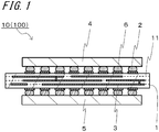
- the imaging component 10 includes: a laminated substrate 1; electrode pads 2 disposed on an upper face of the laminated substrate 1; and conductor patterns 3 disposed between layers of the laminated substrate 1 and electrically connected to the electrode pads 2.
- an imaging module 100 includes: the imaging component 10; and an imaging element 4 mounted on the electrode pads 2 of the imaging component 10.
- the laminated substrate 1 is formed of a resin material.
- a resin material an epoxy resin is used.
- the above-mentioned expression "formed of a resin material” does not necessarily indicate that the laminated substrate is formed of a resin material alone. That is, any other material may be contained.
- a so-called glass epoxy which is constituted such that glass fibers are impregnated with an epoxy resin, or the like may be employed.
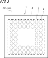
- the laminated substrate 1 may be prepared by laminating glass epoxy substrates. As shown in FIG. 2 , for example, the laminated substrate 1 has a quadrangular-shaped principal surface and is formed in a plat-like shape.
- the vertical dimension can be set to 15 to 20 mm
- the horizontal dimension can be set to 15 to 20 mm
- the thickness can be set to 0.5 to 2 mm.
- the laminated substrate 1 includes a plurality of layers 11.
- the thickness of each of the plurality of layers 11 is 0.05 to 0.2 mm.
- the electrode pad 2 is a member used for mounting the imaging element 4 on the laminated substrate 1.
- the plural electrode pads 2 are disposed on the upper face of the laminated substrate 1.
- the electrode pad 2 has a rectangular shape in a sectional view and a circular shape in a plan view.
- FIG. 2 depicts the situation of the surface of the laminated substrate 1 in a state where the imaging element 4, the electrode pads 2, and solder balls 6 are made as if transparent.
- the electrode pad 2 is formed of a metallic material such as copper or gold.
- the dimensions of the electrode pad 2 for example, in a case where the electrode pad 2 has a circular shape in a plan view, the diameter can be set to 0.1 to 1 mm and the thickness can be set to 0.01 to 0.05 mm.
- a ball grid array or otherwise can be adopted as the method for mounting the imaging element 4. As shown in FIG. 1 , in the imaging component 10 of the present disclosure, the imaging element 4 is mounted by a ball grid array and hence a plurality of solder balls 6 are disposed between a lower face of the imaging element 4 and an upper face of the electrode pads 2.
- the conductor pattern 3 is a member for transmitting a signal generated by the imaging element 4 mounted on the electrode pads 2, to another electronic component 5 such as a monitor.
- the conductor pattern 3 is a belt-shaped member.
- the conductor pattern 3 is disposed between the layers of the laminated substrate 1.
- the conductor pattern 3 is formed of a metallic material such as copper or gold.
- a part of at least one of conductor patterns 3 has a widened portion 31, the widened portion 31 being located immediately below any of electrode pads 2 which are not connected to the at least one of conductor patterns.
- the above-mentioned "widened portion” indicates a portion whose width is widened partly in the conductor pattern 3 extending with a fixed width.
- the imaging component 10 includes: the laminated substrate 1 constituted such that the plurality of layers 11 formed of a resin material are laminated; the plurality of electrode pads 2 disposed on the surface of the laminated substrate 1; and the plurality of conductor patterns 3 disposed between the plurality of layers 11.
- the plurality of conductor patterns 3 have belt shapes. At least one of the plurality of conductor patterns 3 has a first portion 31 and a second portion 32. The first portion 31 overlaps with one of the plurality of electrode pads 2 in a stacking direction of the plurality of layers 11. The second portion 32 does not overlap with the plurality of electrode pads 2 in the stacking direction. The width of the first portion 31 is greater than the width of the second portion 32.
- the conductor patterns 3 may be formed by printing onto the surfaces of the plurality of layers 11 is performed at the time of lamination of the plurality of layers 11.
- each conductor pattern 3 is intentionally simplified into a straight line shape.
- the conductor pattern 3 may be formed in a complicated shape.
- FIGS. 2 and 3 are in correspondence to each other, the arrangement of the conductor patterns 3 in FIG. 1 and the arrangement of the conductor patterns 3 in FIG. 3 are not strictly in correspondence to each other.
- the above-mentioned expression "any of electrode pads 2 which are not connected to the at least one of conductor patterns" does not indicate that the electrode pad 2 and the conductor pattern 3 are completely isolated electrically from each other.
- the expression excludes merely a case where the widened portion 31 of the conductor pattern 3 and the electrode pad 2 located immediately thereabove are directly connected by a through hole or the like. That is, the widened portion 31 and the electrode pad 2 may be indirectly connected through a common power supply or a common ground.
- the imaging component 10 can be obtained in which the conductor patterns 3 are routed at a high density and yet degradation in the positional accuracy of the imaging element 4 is reduced.
- the outer shape of the widened portion 31 may be the same as the outer shape of the electrode pad 2.
- the outer shape of the first portion 31 when viewed from a direction perpendicular to the surface of the laminated substrate 1, the outer shape of the first portion 31 may be the same as the outer shape of the electrode pad 2 overlapping with the first portion 31.
- the above-mentioned expression "the shape is the same” indicates that the shape of the portion of the outer shape of the widened portion 31 in directions other than the extension direction of the conductor pattern 3 is the same as the outer shape of the electrode pad.
- the shape of the portion of the outer shape of the widened portion 31 in directions other than the extension direction of the conductor pattern 3 may be regarded as a circular shape.
- the electrode pad 2 has a circular shape. That is, in the present disclosure, the widened portion 31 and the electrode pad 2 are of the same shape.
- the widened portion 31 of the conductor pattern 3 may be wider than the electrode pad 2.
- the first portion 31 may be wider than the electrode pad 2 overlapping with the first portion 31.
- the conductor pattern 3 can be located immediately below the electrode pad 2. More specifically, for example, in a case where the electrode pad 2 has a circular shape in a plan view, it is sufficient that the wide portion of the conductor pattern 3 is formed in a circular shape larger than the electrode pad 2.
- the first portion 31 when viewed from the direction perpendicular to the surface of the laminated substrate 1, the first portion 31 may be wider than the electrode pad 2 overlapping with the first portion 31, and the centroid of each first portion 31 may be located more distant from the centroid of the laminated substrate 1 than from the centroid of each electrode pad 2 overlapping with the first portion 31.
- the first portions 31 alone of the conductor pattern 3 are shown. More specifically, the centroid of the first portion 31 may be located on an extension line of a straight line joining the centroid of the laminated substrate 1 and the centroid of the electrode pad 2.
- the electrode pad 2 can easily overlap with the first portion 31 even when the position of the electrode pad 2 deviates under heat cycles.
- the first portion 31 may be located in a bent portion of the conductor pattern 3.
- the width of the conductor pattern 3 may be larger in the bent portion of the conductor pattern 3.
- the bent portion of the conductor pattern 3 is susceptible to a thermal stress from other portions. Specifically, in the straight line portion of the conductor pattern 3, thermal expansion in the length direction is mainly caused. In contrast, the bent portion of the conductor pattern 3 receives a thermal stress from the two straight line portions adjacent to the bent portion. Thus, the direction of occurrence of thermal expansion is difficult to be controlled.
- thermal expansion in the bent portion itself can be made larger. By virtue of this, it is possible to reduce a possibility that a thermal stress caused by thermal expansion of other portions results in thermal expansion of the first portion 31 in an unpredictable direction. This can improve the reliability in the imaging component 10 under heat cycles.
- adjacent first portions 31 may be arranged at equal intervals.
- first portions 31 are arranged at equal intervals, it is possible to reduce a possibility of unevenness in the thermal expansion amount caused in the laminated substrate 1 under heat cycles. This can reduce a possibility of distortion in the laminated substrate 1.
Landscapes
- Engineering & Computer Science (AREA)
- Microelectronics & Electronic Packaging (AREA)
- Manufacturing & Machinery (AREA)
- Structure Of Printed Boards (AREA)
- Electric Connection Of Electric Components To Printed Circuits (AREA)
- Production Of Multi-Layered Print Wiring Board (AREA)
- Solid State Image Pick-Up Elements (AREA)
- Physics & Mathematics (AREA)
- Geometry (AREA)
Abstract
Description
- The present disclosure relates to an imaging component and an imaging module provided with the same.
- As an imaging component, for example, there is known a camera module described in Japanese Unexamined Patent Publication
JP-A 2004-104078 Patent Literature 1, hereinafter). The camera module described inPatent Literature 1 includes: a flexible sheet; and an imaging element mounted on a surface of the flexible sheet. - Patent Literature 1: Japanese Unexamined Patent Publication
JP-A 2004-104078 - The imaging component of the present disclosure includes: a laminated substrate formed of a resin material; a plurality of electrode pads disposed on an upper face of the laminated substrate, an imaging element being to be mounted on the plurality of electrode pads; and a plurality of conductor patterns which are belt-shaped and disposed between layers of the laminated substrate, the plurality of conductor patterns being connected to the plurality of the electrode pads, respectively, a part of at least one of the plurality of conductor patterns having a widened portion, the widened portion being located immediately below any of electrode pads which are not connected to the at least one of the plurality of conductor patterns.
-
-
FIG. 1 is a sectional view showing an imaging component and an imaging module; -
FIG. 2 is a schematic diagram showing a situation of a surface of a laminated substrate in an imaging component shown inFIG. 1 ; -
FIG. 3 is a schematic diagram showing wiring shapes of conductor patterns in an imaging component shown inFIG. 1 ; -
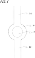
FIG. 4 is a partial transparent plan view showing an electrode pad and a conductor pattern; -
FIG. 5 is a partial transparent plan view showing electrode pads, first portions of conductor patterns, and a laminated substrate; -
FIG. 6 is a partial transparent plan view showing an electrode pad and a conductor pattern; -
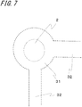
FIG. 7 is a partial transparent plan view showing an electrode pad and a conductor pattern; and -
FIG. 8 is a partial transparent plan view showing an electrode pad and a conductor pattern. - Hereinafter, an
imaging component 10 is described below with reference to the drawings. As shown inFIG. 1 , theimaging component 10 includes: a laminatedsubstrate 1;electrode pads 2 disposed on an upper face of the laminatedsubstrate 1; andconductor patterns 3 disposed between layers of the laminatedsubstrate 1 and electrically connected to theelectrode pads 2. Further, animaging module 100 includes: theimaging component 10; and animaging element 4 mounted on theelectrode pads 2 of theimaging component 10. - The laminated
substrate 1 is formed of a resin material. For example, as the resin material, an epoxy resin is used. Here, the above-mentioned expression "formed of a resin material" does not necessarily indicate that the laminated substrate is formed of a resin material alone. That is, any other material may be contained. Specifically, a so-called glass epoxy which is constituted such that glass fibers are impregnated with an epoxy resin, or the like may be employed. For example, the laminatedsubstrate 1 may be prepared by laminating glass epoxy substrates. As shown inFIG. 2 , for example, the laminatedsubstrate 1 has a quadrangular-shaped principal surface and is formed in a plat-like shape. As for the dimensions of the laminatedsubstrate 1, for example, in a case where the laminatedsubstrate 1 has a quadrangular shape, the vertical dimension can be set to 15 to 20 mm, the horizontal dimension can be set to 15 to 20 mm, and the thickness can be set to 0.5 to 2 mm. More specifically, the laminatedsubstrate 1 includes a plurality oflayers 11. For example, the thickness of each of the plurality oflayers 11 is 0.05 to 0.2 mm. - The
electrode pad 2 is a member used for mounting theimaging element 4 on the laminatedsubstrate 1. Theplural electrode pads 2 are disposed on the upper face of the laminatedsubstrate 1. As shown inFIGS. 1 and2 , for example, theelectrode pad 2 has a rectangular shape in a sectional view and a circular shape in a plan view. Here,FIG. 2 depicts the situation of the surface of the laminatedsubstrate 1 in a state where theimaging element 4, theelectrode pads 2, andsolder balls 6 are made as if transparent. - For example, the
electrode pad 2 is formed of a metallic material such as copper or gold. As for the dimensions of theelectrode pad 2, for example, in a case where theelectrode pad 2 has a circular shape in a plan view, the diameter can be set to 0.1 to 1 mm and the thickness can be set to 0.01 to 0.05 mm. For example, as the method for mounting theimaging element 4, a ball grid array or otherwise can be adopted. As shown inFIG. 1 , in theimaging component 10 of the present disclosure, theimaging element 4 is mounted by a ball grid array and hence a plurality ofsolder balls 6 are disposed between a lower face of theimaging element 4 and an upper face of theelectrode pads 2. - The
conductor pattern 3 is a member for transmitting a signal generated by theimaging element 4 mounted on theelectrode pads 2, to anotherelectronic component 5 such as a monitor. Theconductor pattern 3 is a belt-shaped member. Theconductor pattern 3 is disposed between the layers of the laminatedsubstrate 1. For example, theconductor pattern 3 is formed of a metallic material such as copper or gold. - Here, in the
imaging component 10 of the present disclosure, as shown inFIGS. 2 and3 , a part of at least one ofconductor patterns 3 has a widenedportion 31, the widenedportion 31 being located immediately below any ofelectrode pads 2 which are not connected to the at least one of conductor patterns. Here, the above-mentioned "widened portion" indicates a portion whose width is widened partly in theconductor pattern 3 extending with a fixed width. Specifically, as shown inFIG. 3 , in a case where theconductor pattern 3 extends in a belt shape, imaginary lines perpendicular to an extension direction of theconductor pattern 3 are drawn at a location where the width of theconductor pattern 3 begins to change when viewed in the extension direction of theconductor pattern 3 and at a location where the width change ends. Then, a region of theconductor pattern 3 located between the two imaginary lines is regarded as the widenedportion 31. - In other words, the
imaging component 10 includes: the laminatedsubstrate 1 constituted such that the plurality oflayers 11 formed of a resin material are laminated; the plurality ofelectrode pads 2 disposed on the surface of the laminatedsubstrate 1; and the plurality ofconductor patterns 3 disposed between the plurality oflayers 11. The plurality ofconductor patterns 3 have belt shapes. At least one of the plurality ofconductor patterns 3 has afirst portion 31 and asecond portion 32. Thefirst portion 31 overlaps with one of the plurality ofelectrode pads 2 in a stacking direction of the plurality oflayers 11. Thesecond portion 32 does not overlap with the plurality ofelectrode pads 2 in the stacking direction. The width of thefirst portion 31 is greater than the width of thesecond portion 32. Theconductor patterns 3 may be formed by printing onto the surfaces of the plurality oflayers 11 is performed at the time of lamination of the plurality oflayers 11. - Here, in the
conductor patterns 3 shown inFIG. 3 , for simplicity of understanding, eachconductor pattern 3 is intentionally simplified into a straight line shape. Theconductor pattern 3 may be formed in a complicated shape. Thus, althoughFIGS. 2 and3 are in correspondence to each other, the arrangement of theconductor patterns 3 inFIG. 1 and the arrangement of theconductor patterns 3 inFIG. 3 are not strictly in correspondence to each other. Further, the above-mentioned expression "any ofelectrode pads 2 which are not connected to the at least one of conductor patterns" does not indicate that theelectrode pad 2 and theconductor pattern 3 are completely isolated electrically from each other. Specifically, the expression excludes merely a case where the widenedportion 31 of theconductor pattern 3 and theelectrode pad 2 located immediately thereabove are directly connected by a through hole or the like. That is, the widenedportion 31 and theelectrode pad 2 may be indirectly connected through a common power supply or a common ground. - When the portion of the
conductor pattern 3 located immediately below theelectrode pad 2 has the widenedportion 31 as described above, it is possible to reduce a situation that the portion of the laminatedsubstrate 1 immediately below theelectrode pad 2 sinks. Further, when in a region other than the portion of theconductor pattern 3 located immediately below theelectrode pad 2, the width is made narrower than that of the portion located immediately below theelectrode pad 2, high-density routing of theconductor patterns 3 is possible. As a result, theimaging component 10 can be obtained in which theconductor patterns 3 are routed at a high density and yet degradation in the positional accuracy of theimaging element 4 is reduced. - Here, in a transparent plane view, the outer shape of the widened
portion 31 may be the same as the outer shape of theelectrode pad 2. In other words, when viewed from a direction perpendicular to the surface of thelaminated substrate 1, the outer shape of thefirst portion 31 may be the same as the outer shape of theelectrode pad 2 overlapping with thefirst portion 31. When such a configuration is employed, it is possible to reduce unevenness in the stress in the surface of theconductor pattern 3 transmitted from theelectrode pad 2. Then, this can reduce deformation caused in theimaging component 10. - Here, the above-mentioned expression "the shape is the same" indicates that the shape of the portion of the outer shape of the widened
portion 31 in directions other than the extension direction of theconductor pattern 3 is the same as the outer shape of the electrode pad. For example, inFIG. 3 , the shape of the portion of the outer shape of the widenedportion 31 in directions other than the extension direction of theconductor pattern 3 may be regarded as a circular shape. Then, as shown inFIG. 2 , theelectrode pad 2 has a circular shape. That is, in the present disclosure, the widenedportion 31 and theelectrode pad 2 are of the same shape. - Further, as shown in
FIG. 4 , the widenedportion 31 of theconductor pattern 3 may be wider than theelectrode pad 2. In other words, when viewed from the direction perpendicular to the surface of thelaminated substrate 1, thefirst portion 31 may be wider than theelectrode pad 2 overlapping with thefirst portion 31. By virtue of this, even when the deviation in the positional relation between theelectrode pad 2 and theconductor pattern 3 is caused under heat cycles, theconductor pattern 3 can be located immediately below theelectrode pad 2. More specifically, for example, in a case where theelectrode pad 2 has a circular shape in a plan view, it is sufficient that the wide portion of theconductor pattern 3 is formed in a circular shape larger than theelectrode pad 2. - Further, as shown in
FIGS. 5 and6 , when viewed from the direction perpendicular to the surface of thelaminated substrate 1, thefirst portion 31 may be wider than theelectrode pad 2 overlapping with thefirst portion 31, and the centroid of eachfirst portion 31 may be located more distant from the centroid of thelaminated substrate 1 than from the centroid of eachelectrode pad 2 overlapping with thefirst portion 31. InFIG. 5 , for simplicity of understanding, thefirst portions 31 alone of theconductor pattern 3 are shown. More specifically, the centroid of thefirst portion 31 may be located on an extension line of a straight line joining the centroid of thelaminated substrate 1 and the centroid of theelectrode pad 2. - Under heat cycles, larger thermal expansion and larger thermal contraction are caused in the surface than in the inside of the
laminated substrate 1. In a case where the width of thefirst portion 31 is made larger than the width of theelectrode pad 2 and the centroid thereof is deviated to the outer side of thelaminated substrate 1, theelectrode pad 2 can easily overlap with thefirst portion 31 even when the position of theelectrode pad 2 deviates under heat cycles. - Further, as shown in
FIG. 7 , thefirst portion 31 may be located in a bent portion of theconductor pattern 3. In other words, the width of theconductor pattern 3 may be larger in the bent portion of theconductor pattern 3. In general, the bent portion of theconductor pattern 3 is susceptible to a thermal stress from other portions. Specifically, in the straight line portion of theconductor pattern 3, thermal expansion in the length direction is mainly caused. In contrast, the bent portion of theconductor pattern 3 receives a thermal stress from the two straight line portions adjacent to the bent portion. Thus, the direction of occurrence of thermal expansion is difficult to be controlled. Here, as shown inFIG. 7 , when thefirst portion 31 is located in the bent portion of theconductor pattern 3, thermal expansion in the bent portion itself can be made larger. By virtue of this, it is possible to reduce a possibility that a thermal stress caused by thermal expansion of other portions results in thermal expansion of thefirst portion 31 in an unpredictable direction. This can improve the reliability in theimaging component 10 under heat cycles. - Further, as shown in
FIG. 8 , adjacentfirst portions 31 may be arranged at equal intervals. When thefirst portions 31 are arranged at equal intervals, it is possible to reduce a possibility of unevenness in the thermal expansion amount caused in thelaminated substrate 1 under heat cycles. This can reduce a possibility of distortion in thelaminated substrate 1. -
- 1: Laminated substrate
- 11: Layer
- 2: Electrode pad
- 3: Conductor pattern
- 31: Widened portion
- 4: Imaging element
- 5: Electronic component
- 10: Imaging component
- 100: Imaging module
Claims (8)
- An imaging component, comprising:a laminated substrate formed of a resin material;a plurality of electrode pads disposed on an upper face of the laminated substrate, an imaging element being to be mounted on the plurality of electrodes; anda plurality of conductor patterns which are belt-shaped and disposed between layers of the laminated substrate, the plurality of conductor patterns being connected to the plurality of electrode pads, respectively,a part of at least one of the plurality of conductor patterns having a widened portion, the widened portion being located immediately below any of electrode pads which are not connected to the at least one of the plurality of conductor patterns.
- The imaging component according to claim 1, wherein in a transparent plane view of the imaging component, an outer shape of the widened portion is a same as an outer shape of the electrode pad.
- An imaging module, comprising:the imaging component according to claim 1 or 2; andan imaging element mounted on the electrode pads of the imaging component.
- An imaging component, comprising:a laminated substrate constituted such that a plurality of layers formed of a resin material are laminated;a plurality of electrode pads disposed on a surface of the laminated substrate; anda plurality of conductor patterns disposed between the plurality of layers,the plurality of conductor patterns having belt shapes, at least one of the plurality of conductor patterns having a first portion and a second portion, the first portion overlapping with one of the plurality of electrode pads in a stacking direction of the plurality of layers, the second portion not overlapping with the plurality of electrode pads in the stacking direction, a width of the first portion being greater than a width of the second portion.
- The imaging component according to claim 4, wherein when viewed from a direction perpendicular to the surface, an outer shape of the first portion is a same as an outer shape of the one of the plurality of electrode pads overlapping with the first portion.
- The imaging component according to claim 4, wherein when viewed from a direction perpendicular to the surface, the first portion is wider than the one of the plurality of electrode pads overlapping with the first portion.
- The imaging component according to claim 6, wherein when viewed from a direction perpendicular to the surface, a centroid of the first portion is located more distant from a centroid of the laminated substrate than from a centroid of the one of the plurality of electrode pads overlapping with the first portion.
- An imaging module, comprising:the imaging component according to any one of claims 4 to 7; andan imaging element mounted on the plurality of electrode pads of the imaging component.
Applications Claiming Priority (2)
| Application Number | Priority Date | Filing Date | Title |
|---|---|---|---|
| JP2015067248 | 2015-03-27 | ||
| PCT/JP2016/055575 WO2016158109A1 (en) | 2015-03-27 | 2016-02-25 | Imaging component, and imaging module provided with same |
Publications (3)
| Publication Number | Publication Date |
|---|---|
| EP3277065A1 true EP3277065A1 (en) | 2018-01-31 |
| EP3277065A4 EP3277065A4 (en) | 2018-12-12 |
| EP3277065B1 EP3277065B1 (en) | 2021-08-11 |
Family
ID=57005690
Family Applications (1)
| Application Number | Title | Priority Date | Filing Date |
|---|---|---|---|
| EP16771993.9A Active EP3277065B1 (en) | 2015-03-27 | 2016-02-25 | Imaging component, and imaging module provided with same |
Country Status (5)
| Country | Link |
|---|---|
| US (1) | US20180130841A1 (en) |
| EP (1) | EP3277065B1 (en) |
| JP (1) | JP6454001B2 (en) |
| CN (1) | CN107409471B (en) |
| WO (1) | WO2016158109A1 (en) |
Families Citing this family (1)
| Publication number | Priority date | Publication date | Assignee | Title |
|---|---|---|---|---|
| DE102017128568A1 (en) * | 2017-12-01 | 2019-06-06 | Infineon Technologies Ag | SEMICONDUCTOR CHIP WITH A VARIETY OF EXTERNAL CONTACTS, CHIP ARRANGEMENT AND METHOD FOR CHECKING AN ORIENTATION OF A POSITION OF A SEMICONDUCTOR CHIP |
Family Cites Families (26)
| Publication number | Priority date | Publication date | Assignee | Title |
|---|---|---|---|---|
| JPS5535820Y2 (en) * | 1974-09-11 | 1980-08-23 | ||
| JPS60175494A (en) * | 1984-02-20 | 1985-09-09 | 松下電器産業株式会社 | Method of producing metal base circuit board |
| JPH04286392A (en) * | 1991-03-15 | 1992-10-12 | Fujitsu Ltd | Printed circuit board |
| JPH05152382A (en) * | 1991-12-02 | 1993-06-18 | Matsushita Electric Ind Co Ltd | Circuit device |
| ATE166202T1 (en) * | 1991-12-31 | 1998-05-15 | Tessera Inc | METHOD FOR CONSTRUCTING MULTI-LAYER CIRCUITS, STRUCTURES WITH PERSONALIZATION FEATURES AND COMPONENTS USED THEREIN |
| JPH05235547A (en) * | 1992-02-26 | 1993-09-10 | Fujitsu Ltd | Wiring structure for thin film board |
| JPH06326214A (en) * | 1993-05-17 | 1994-11-25 | Nkk Corp | Multilayer wiring structure and method of forming the same |
| JPH07106764A (en) * | 1993-10-08 | 1995-04-21 | Fujitsu Ltd | Ceramic multilayer circuit board |
| JPH09223715A (en) * | 1996-02-15 | 1997-08-26 | Pfu Ltd | Flip chip or flip chip carrier connection structure |
| JPH11307886A (en) * | 1998-04-21 | 1999-11-05 | Matsushita Electric Ind Co Ltd | Flip chip bonded land undulation prevention pattern |
| JP2000208665A (en) * | 1999-01-13 | 2000-07-28 | Pfu Ltd | Small semiconductor device and mounting structure of small semiconductor device |
| US6879492B2 (en) * | 2001-03-28 | 2005-04-12 | International Business Machines Corporation | Hyperbga buildup laminate |
| JP2004104078A (en) * | 2002-06-28 | 2004-04-02 | Sanyo Electric Co Ltd | Camera module and manufacturing method thereof |
| JP2004214586A (en) * | 2002-11-14 | 2004-07-29 | Kyocera Corp | Multilayer wiring board |
| JP2005268259A (en) * | 2004-03-16 | 2005-09-29 | Kyocera Corp | Multilayer wiring board |
| JP4304163B2 (en) * | 2005-03-09 | 2009-07-29 | パナソニック株式会社 | Imaging module and manufacturing method thereof |
| TW201101476A (en) * | 2005-06-02 | 2011-01-01 | Sony Corp | Semiconductor image sensor module and method of manufacturing the same |
| JP2008227429A (en) * | 2007-03-16 | 2008-09-25 | Alps Electric Co Ltd | Electronic circuit module and multilayer wiring board |
| JP5407667B2 (en) * | 2008-11-05 | 2014-02-05 | 株式会社村田製作所 | Semiconductor device |
| WO2010131529A1 (en) * | 2009-05-12 | 2010-11-18 | 株式会社村田製作所 | Circuit board and method for manufacturing same |
| JP5547594B2 (en) * | 2010-09-28 | 2014-07-16 | 新光電気工業株式会社 | WIRING BOARD, SEMICONDUCTOR DEVICE, AND WIRING BOARD MANUFACTURING METHOD |
| JP2013093538A (en) * | 2011-10-04 | 2013-05-16 | Ngk Spark Plug Co Ltd | Wiring board and manufacturing method of the same |
| WO2014054353A1 (en) * | 2012-10-05 | 2014-04-10 | 株式会社村田製作所 | Electronic component-embedded module and communication terminal |
| US9560771B2 (en) * | 2012-11-27 | 2017-01-31 | Omnivision Technologies, Inc. | Ball grid array and land grid array having modified footprint |
| US9117825B2 (en) * | 2012-12-06 | 2015-08-25 | Taiwan Semiconductor Manufacturing Company, Ltd. | Substrate pad structure |
| KR102214512B1 (en) * | 2014-07-04 | 2021-02-09 | 삼성전자 주식회사 | Printed circuit board and semiconductor package using the same |
-
2016
- 2016-02-25 JP JP2017509390A patent/JP6454001B2/en active Active
- 2016-02-25 WO PCT/JP2016/055575 patent/WO2016158109A1/en not_active Ceased
- 2016-02-25 CN CN201680014936.7A patent/CN107409471B/en active Active
- 2016-02-25 EP EP16771993.9A patent/EP3277065B1/en active Active
- 2016-02-25 US US15/561,872 patent/US20180130841A1/en not_active Abandoned
Also Published As
| Publication number | Publication date |
|---|---|
| JPWO2016158109A1 (en) | 2017-12-28 |
| US20180130841A1 (en) | 2018-05-10 |
| EP3277065A4 (en) | 2018-12-12 |
| JP6454001B2 (en) | 2019-01-16 |
| EP3277065B1 (en) | 2021-08-11 |
| CN107409471B (en) | 2020-07-21 |
| WO2016158109A1 (en) | 2016-10-06 |
| CN107409471A (en) | 2017-11-28 |
Similar Documents
| Publication | Publication Date | Title |
|---|---|---|
| CN106171049B (en) | Electronic equipment | |
| KR101815754B1 (en) | Semiconductor device | |
| EP2930557B1 (en) | Electric component | |
| US11877392B2 (en) | Flexible wiring board, module, and electronic device | |
| CN110740563B (en) | Wiring board | |
| US9950512B2 (en) | Liquid discharge head | |
| US20150250047A1 (en) | Flexible printed circuit board, planar light source apparatus, display apparatus, and electronic device | |
| EP3277065A1 (en) | Imaging component, and imaging module provided with same | |
| US9922918B2 (en) | Substrate for stacked module, stacked module, and method for manufacturing stacked module | |
| US20200258805A1 (en) | Electronic component module provided with substrate on which electronic components are mounted and heat sink and manufacturing method of the same | |
| US20150027762A1 (en) | Printed circuit board | |
| JP2017022225A (en) | Circuit board and electronic device | |
| KR101888425B1 (en) | Flexible printed circuits board | |
| JP4488073B2 (en) | Electrical connection device | |
| JP5651096B2 (en) | Flexible printed circuit board and flat display device | |
| US10188000B2 (en) | Component mounting board | |
| US9888575B2 (en) | Electronic device and method for manufacturing electronic device | |
| KR101313684B1 (en) | Soldering joint structrue of printed circuit board with excellent solder discharging property | |
| US20160205782A1 (en) | Printed circuit board and method for fabricating the same | |
| KR101365991B1 (en) | Joint structrue of printed circuit board with excellent prevention efficiency on heat transformation | |
| KR20050073417A (en) | Electronic component, method for manufacturing the electronic component, and electronic apparatus | |
| KR20130077456A (en) | Flexible printed circuit board | |
| US8901432B2 (en) | Mitigation of block bending in a ring laser gyroscope caused by thermal expansion or compression of a circuit board | |
| US9502456B2 (en) | Electronic component device | |
| JP2015130424A (en) | Printed wiring board, printed circuit board and printed circuit board manufacturing method |
Legal Events
| Date | Code | Title | Description |
|---|---|---|---|
| STAA | Information on the status of an ep patent application or granted ep patent |
Free format text: STATUS: THE INTERNATIONAL PUBLICATION HAS BEEN MADE |
|
| PUAI | Public reference made under article 153(3) epc to a published international application that has entered the european phase |
Free format text: ORIGINAL CODE: 0009012 |
|
| STAA | Information on the status of an ep patent application or granted ep patent |
Free format text: STATUS: REQUEST FOR EXAMINATION WAS MADE |
|
| 17P | Request for examination filed |
Effective date: 20170926 |
|
| AK | Designated contracting states |
Kind code of ref document: A1 Designated state(s): AL AT BE BG CH CY CZ DE DK EE ES FI FR GB GR HR HU IE IS IT LI LT LU LV MC MK MT NL NO PL PT RO RS SE SI SK SM TR |
|
| AX | Request for extension of the european patent |
Extension state: BA ME |
|
| DAV | Request for validation of the european patent (deleted) | ||
| DAX | Request for extension of the european patent (deleted) | ||
| A4 | Supplementary search report drawn up and despatched |
Effective date: 20181112 |
|
| RIC1 | Information provided on ipc code assigned before grant |
Ipc: H05K 3/46 20060101AFI20181106BHEP Ipc: H01L 23/538 20060101ALI20181106BHEP Ipc: H01L 23/12 20060101ALI20181106BHEP Ipc: H05K 1/02 20060101ALI20181106BHEP Ipc: H01L 27/14 20060101ALI20181106BHEP |
|
| RIC1 | Information provided on ipc code assigned before grant |
Ipc: H01L 27/146 20060101ALI20210301BHEP Ipc: H01L 27/14 20060101ALI20210301BHEP Ipc: H01L 23/12 20060101ALI20210301BHEP Ipc: H05K 1/02 20060101ALI20210301BHEP Ipc: H05K 3/46 20060101AFI20210301BHEP Ipc: H01L 23/538 20060101ALI20210301BHEP |
|
| GRAP | Despatch of communication of intention to grant a patent |
Free format text: ORIGINAL CODE: EPIDOSNIGR1 |
|
| STAA | Information on the status of an ep patent application or granted ep patent |
Free format text: STATUS: GRANT OF PATENT IS INTENDED |
|
| INTG | Intention to grant announced |
Effective date: 20210414 |
|
| GRAS | Grant fee paid |
Free format text: ORIGINAL CODE: EPIDOSNIGR3 |
|
| GRAA | (expected) grant |
Free format text: ORIGINAL CODE: 0009210 |
|
| STAA | Information on the status of an ep patent application or granted ep patent |
Free format text: STATUS: THE PATENT HAS BEEN GRANTED |
|
| AK | Designated contracting states |
Kind code of ref document: B1 Designated state(s): AL AT BE BG CH CY CZ DE DK EE ES FI FR GB GR HR HU IE IS IT LI LT LU LV MC MK MT NL NO PL PT RO RS SE SI SK SM TR |
|
| REG | Reference to a national code |
Ref country code: CH Ref legal event code: EP |
|
| REG | Reference to a national code |
Ref country code: DE Ref legal event code: R096 Ref document number: 602016062045 Country of ref document: DE |
|
| REG | Reference to a national code |
Ref country code: IE Ref legal event code: FG4D Ref country code: AT Ref legal event code: REF Ref document number: 1420758 Country of ref document: AT Kind code of ref document: T Effective date: 20210915 |
|
| REG | Reference to a national code |
Ref country code: LT Ref legal event code: MG9D |
|
| REG | Reference to a national code |
Ref country code: NL Ref legal event code: MP Effective date: 20210811 |
|
| REG | Reference to a national code |
Ref country code: AT Ref legal event code: MK05 Ref document number: 1420758 Country of ref document: AT Kind code of ref document: T Effective date: 20210811 |
|
| PG25 | Lapsed in a contracting state [announced via postgrant information from national office to epo] |
Ref country code: HR Free format text: LAPSE BECAUSE OF FAILURE TO SUBMIT A TRANSLATION OF THE DESCRIPTION OR TO PAY THE FEE WITHIN THE PRESCRIBED TIME-LIMIT Effective date: 20210811 Ref country code: FI Free format text: LAPSE BECAUSE OF FAILURE TO SUBMIT A TRANSLATION OF THE DESCRIPTION OR TO PAY THE FEE WITHIN THE PRESCRIBED TIME-LIMIT Effective date: 20210811 Ref country code: ES Free format text: LAPSE BECAUSE OF FAILURE TO SUBMIT A TRANSLATION OF THE DESCRIPTION OR TO PAY THE FEE WITHIN THE PRESCRIBED TIME-LIMIT Effective date: 20210811 Ref country code: NO Free format text: LAPSE BECAUSE OF FAILURE TO SUBMIT A TRANSLATION OF THE DESCRIPTION OR TO PAY THE FEE WITHIN THE PRESCRIBED TIME-LIMIT Effective date: 20211111 Ref country code: PT Free format text: LAPSE BECAUSE OF FAILURE TO SUBMIT A TRANSLATION OF THE DESCRIPTION OR TO PAY THE FEE WITHIN THE PRESCRIBED TIME-LIMIT Effective date: 20211213 Ref country code: LT Free format text: LAPSE BECAUSE OF FAILURE TO SUBMIT A TRANSLATION OF THE DESCRIPTION OR TO PAY THE FEE WITHIN THE PRESCRIBED TIME-LIMIT Effective date: 20210811 Ref country code: AT Free format text: LAPSE BECAUSE OF FAILURE TO SUBMIT A TRANSLATION OF THE DESCRIPTION OR TO PAY THE FEE WITHIN THE PRESCRIBED TIME-LIMIT Effective date: 20210811 Ref country code: BG Free format text: LAPSE BECAUSE OF FAILURE TO SUBMIT A TRANSLATION OF THE DESCRIPTION OR TO PAY THE FEE WITHIN THE PRESCRIBED TIME-LIMIT Effective date: 20211111 Ref country code: SE Free format text: LAPSE BECAUSE OF FAILURE TO SUBMIT A TRANSLATION OF THE DESCRIPTION OR TO PAY THE FEE WITHIN THE PRESCRIBED TIME-LIMIT Effective date: 20210811 Ref country code: RS Free format text: LAPSE BECAUSE OF FAILURE TO SUBMIT A TRANSLATION OF THE DESCRIPTION OR TO PAY THE FEE WITHIN THE PRESCRIBED TIME-LIMIT Effective date: 20210811 |
|
| PG25 | Lapsed in a contracting state [announced via postgrant information from national office to epo] |
Ref country code: PL Free format text: LAPSE BECAUSE OF FAILURE TO SUBMIT A TRANSLATION OF THE DESCRIPTION OR TO PAY THE FEE WITHIN THE PRESCRIBED TIME-LIMIT Effective date: 20210811 Ref country code: LV Free format text: LAPSE BECAUSE OF FAILURE TO SUBMIT A TRANSLATION OF THE DESCRIPTION OR TO PAY THE FEE WITHIN THE PRESCRIBED TIME-LIMIT Effective date: 20210811 Ref country code: GR Free format text: LAPSE BECAUSE OF FAILURE TO SUBMIT A TRANSLATION OF THE DESCRIPTION OR TO PAY THE FEE WITHIN THE PRESCRIBED TIME-LIMIT Effective date: 20211112 |
|
| PG25 | Lapsed in a contracting state [announced via postgrant information from national office to epo] |
Ref country code: NL Free format text: LAPSE BECAUSE OF FAILURE TO SUBMIT A TRANSLATION OF THE DESCRIPTION OR TO PAY THE FEE WITHIN THE PRESCRIBED TIME-LIMIT Effective date: 20210811 |
|
| PG25 | Lapsed in a contracting state [announced via postgrant information from national office to epo] |
Ref country code: DK Free format text: LAPSE BECAUSE OF FAILURE TO SUBMIT A TRANSLATION OF THE DESCRIPTION OR TO PAY THE FEE WITHIN THE PRESCRIBED TIME-LIMIT Effective date: 20210811 |
|
| REG | Reference to a national code |
Ref country code: DE Ref legal event code: R097 Ref document number: 602016062045 Country of ref document: DE |
|
| PG25 | Lapsed in a contracting state [announced via postgrant information from national office to epo] |
Ref country code: SM Free format text: LAPSE BECAUSE OF FAILURE TO SUBMIT A TRANSLATION OF THE DESCRIPTION OR TO PAY THE FEE WITHIN THE PRESCRIBED TIME-LIMIT Effective date: 20210811 Ref country code: SK Free format text: LAPSE BECAUSE OF FAILURE TO SUBMIT A TRANSLATION OF THE DESCRIPTION OR TO PAY THE FEE WITHIN THE PRESCRIBED TIME-LIMIT Effective date: 20210811 Ref country code: RO Free format text: LAPSE BECAUSE OF FAILURE TO SUBMIT A TRANSLATION OF THE DESCRIPTION OR TO PAY THE FEE WITHIN THE PRESCRIBED TIME-LIMIT Effective date: 20210811 Ref country code: EE Free format text: LAPSE BECAUSE OF FAILURE TO SUBMIT A TRANSLATION OF THE DESCRIPTION OR TO PAY THE FEE WITHIN THE PRESCRIBED TIME-LIMIT Effective date: 20210811 Ref country code: CZ Free format text: LAPSE BECAUSE OF FAILURE TO SUBMIT A TRANSLATION OF THE DESCRIPTION OR TO PAY THE FEE WITHIN THE PRESCRIBED TIME-LIMIT Effective date: 20210811 Ref country code: AL Free format text: LAPSE BECAUSE OF FAILURE TO SUBMIT A TRANSLATION OF THE DESCRIPTION OR TO PAY THE FEE WITHIN THE PRESCRIBED TIME-LIMIT Effective date: 20210811 |
|
| PLBE | No opposition filed within time limit |
Free format text: ORIGINAL CODE: 0009261 |
|
| STAA | Information on the status of an ep patent application or granted ep patent |
Free format text: STATUS: NO OPPOSITION FILED WITHIN TIME LIMIT |
|
| 26N | No opposition filed |
Effective date: 20220512 |
|
| PG25 | Lapsed in a contracting state [announced via postgrant information from national office to epo] |
Ref country code: IT Free format text: LAPSE BECAUSE OF FAILURE TO SUBMIT A TRANSLATION OF THE DESCRIPTION OR TO PAY THE FEE WITHIN THE PRESCRIBED TIME-LIMIT Effective date: 20210811 |
|
| PG25 | Lapsed in a contracting state [announced via postgrant information from national office to epo] |
Ref country code: SI Free format text: LAPSE BECAUSE OF FAILURE TO SUBMIT A TRANSLATION OF THE DESCRIPTION OR TO PAY THE FEE WITHIN THE PRESCRIBED TIME-LIMIT Effective date: 20210811 |
|
| PG25 | Lapsed in a contracting state [announced via postgrant information from national office to epo] |
Ref country code: MC Free format text: LAPSE BECAUSE OF FAILURE TO SUBMIT A TRANSLATION OF THE DESCRIPTION OR TO PAY THE FEE WITHIN THE PRESCRIBED TIME-LIMIT Effective date: 20210811 |
|
| REG | Reference to a national code |
Ref country code: CH Ref legal event code: PL |
|
| REG | Reference to a national code |
Ref country code: BE Ref legal event code: MM Effective date: 20220228 |
|
| PG25 | Lapsed in a contracting state [announced via postgrant information from national office to epo] |
Ref country code: LU Free format text: LAPSE BECAUSE OF NON-PAYMENT OF DUE FEES Effective date: 20220225 |
|
| PG25 | Lapsed in a contracting state [announced via postgrant information from national office to epo] |
Ref country code: LI Free format text: LAPSE BECAUSE OF NON-PAYMENT OF DUE FEES Effective date: 20220228 Ref country code: IE Free format text: LAPSE BECAUSE OF NON-PAYMENT OF DUE FEES Effective date: 20220225 Ref country code: CH Free format text: LAPSE BECAUSE OF NON-PAYMENT OF DUE FEES Effective date: 20220228 |
|
| PG25 | Lapsed in a contracting state [announced via postgrant information from national office to epo] |
Ref country code: BE Free format text: LAPSE BECAUSE OF NON-PAYMENT OF DUE FEES Effective date: 20220228 |
|
| P01 | Opt-out of the competence of the unified patent court (upc) registered |
Effective date: 20230505 |
|
| PG25 | Lapsed in a contracting state [announced via postgrant information from national office to epo] |
Ref country code: HU Free format text: LAPSE BECAUSE OF FAILURE TO SUBMIT A TRANSLATION OF THE DESCRIPTION OR TO PAY THE FEE WITHIN THE PRESCRIBED TIME-LIMIT; INVALID AB INITIO Effective date: 20160225 |
|
| PG25 | Lapsed in a contracting state [announced via postgrant information from national office to epo] |
Ref country code: MK Free format text: LAPSE BECAUSE OF FAILURE TO SUBMIT A TRANSLATION OF THE DESCRIPTION OR TO PAY THE FEE WITHIN THE PRESCRIBED TIME-LIMIT Effective date: 20210811 Ref country code: CY Free format text: LAPSE BECAUSE OF FAILURE TO SUBMIT A TRANSLATION OF THE DESCRIPTION OR TO PAY THE FEE WITHIN THE PRESCRIBED TIME-LIMIT Effective date: 20210811 |
|
| PG25 | Lapsed in a contracting state [announced via postgrant information from national office to epo] |
Ref country code: MT Free format text: LAPSE BECAUSE OF FAILURE TO SUBMIT A TRANSLATION OF THE DESCRIPTION OR TO PAY THE FEE WITHIN THE PRESCRIBED TIME-LIMIT Effective date: 20210811 |
|
| PGFP | Annual fee paid to national office [announced via postgrant information from national office to epo] |
Ref country code: FR Payment date: 20241231 Year of fee payment: 10 |
|
| PGFP | Annual fee paid to national office [announced via postgrant information from national office to epo] |
Ref country code: DE Payment date: 20241231 Year of fee payment: 10 |
|
| PGFP | Annual fee paid to national office [announced via postgrant information from national office to epo] |
Ref country code: GB Payment date: 20250102 Year of fee payment: 10 |
|
| PG25 | Lapsed in a contracting state [announced via postgrant information from national office to epo] |
Ref country code: TR Free format text: LAPSE BECAUSE OF FAILURE TO SUBMIT A TRANSLATION OF THE DESCRIPTION OR TO PAY THE FEE WITHIN THE PRESCRIBED TIME-LIMIT Effective date: 20210811 |