EP3272011B1 - Commutateur analogique à fuite de drain induite par la grille réduite - Google Patents
Commutateur analogique à fuite de drain induite par la grille réduite Download PDFInfo
- Publication number
- EP3272011B1 EP3272011B1 EP16711958.5A EP16711958A EP3272011B1 EP 3272011 B1 EP3272011 B1 EP 3272011B1 EP 16711958 A EP16711958 A EP 16711958A EP 3272011 B1 EP3272011 B1 EP 3272011B1
- Authority
- EP
- European Patent Office
- Prior art keywords
- switch
- coupled
- gate
- channel transistor
- buffer
- Prior art date
- Legal status (The legal status is an assumption and is not a legal conclusion. Google has not performed a legal analysis and makes no representation as to the accuracy of the status listed.)
- Active
Links
Images


Classifications
-
- H—ELECTRICITY
- H03—ELECTRONIC CIRCUITRY
- H03K—PULSE TECHNIQUE
- H03K17/00—Electronic switching or gating, i.e. not by contact-making and –breaking
- H03K17/16—Modifications for eliminating interference voltages or currents
- H03K17/161—Modifications for eliminating interference voltages or currents in field-effect transistor switches
-
- H—ELECTRICITY
- H03—ELECTRONIC CIRCUITRY
- H03K—PULSE TECHNIQUE
- H03K17/00—Electronic switching or gating, i.e. not by contact-making and –breaking
- H03K17/06—Modifications for ensuring a fully conducting state
- H03K17/063—Modifications for ensuring a fully conducting state in field-effect transistor switches
-
- H—ELECTRICITY
- H03—ELECTRONIC CIRCUITRY
- H03K—PULSE TECHNIQUE
- H03K17/00—Electronic switching or gating, i.e. not by contact-making and –breaking
- H03K17/16—Modifications for eliminating interference voltages or currents
- H03K17/161—Modifications for eliminating interference voltages or currents in field-effect transistor switches
- H03K17/165—Modifications for eliminating interference voltages or currents in field-effect transistor switches by feedback from the output circuit to the control circuit
-
- H—ELECTRICITY
- H03—ELECTRONIC CIRCUITRY
- H03K—PULSE TECHNIQUE
- H03K3/00—Circuits for generating electric pulses; Monostable, bistable or multistable circuits
- H03K3/01—Details
- H03K3/012—Modifications of generator to improve response time or to decrease power consumption
-
- H—ELECTRICITY
- H03—ELECTRONIC CIRCUITRY
- H03K—PULSE TECHNIQUE
- H03K2217/00—Indexing scheme related to electronic switching or gating, i.e. not by contact-making or -breaking covered by H03K17/00
- H03K2217/0054—Gating switches, e.g. pass gates
Definitions
- Examples of the present disclosure generally relate to electronic circuits and, in particular, to an analog switch having reduced gate-induced drain leakage.
- a basic complementary metal oxide semiconductor (CMOS) switch comprises an N-channel transistor in parallel with a P-channel transistor.
- the sources of the N- and P-channel transistors comprise an input of the switch, and the drains of the N- and P-channel transistors comprise an output of the switch.
- the gates of the N- and P-channel transistors are coupled to complementary enable signals that control the state of the CMOS switch.
- An enable signal is coupled to the gate of the N-channel transistor, and a complement of the enable signal is coupled to the gate of the P-channel transistor.
- GIDL gate-induced drain leakage
- MOS metal oxide semiconductor
- GIDL depends on drain-to-body voltage and drain-to-gate voltage.
- a circuit can include several CMOS switches coupled to a common terminal (e.g., a multiplexer or de-multiplexer) such that, during operation, only one CMOS switch is in the on-state and the rest of the CMOS switches are in the off-state.
- the GIDL currents combine and scale based on the number of switches in the off-state.
- the combined GIDL current can significantly impact performance of the system, particularly if the CMOS switches are operated as analog switches.
- an apparatus includes an analog switch having an n-type metal oxide semiconductor (NMOS) circuit in parallel with a p-type metal oxide semiconductor (PMOS) circuit between a switch input and a switch output.
- the analog switch is responsive to an enable signal that determines switch state thereof.
- the NMOS circuit includes a switch N-channel transistor coupled to a buffer N-channel transistor, a gate of the switch N-channel transistor coupled to the enable signal and a gate of the buffer N-channel transistor coupled to a modulated N-channel gate voltage.
- the PMOS circuit including a switch P-channel transistor coupled to a buffer P-channel transistor, a gate of the switch P-channel transistor coupled to a complement of the enable signal and a gate of the buffer P-channel transistor coupled to a modulated P-channel gate voltage.
- a control circuit is coupled to the analog switch to provide the modulated N-channel and modulated P-channel gate voltages each of which alternates between a respective supply voltage and a respective GIDL mitigation voltage based on the switch state.
- an apparatus in another example, includes a plurality of analog switches coupled to a common terminal. Each of the plurality of analog switches responsive to a respective enable signal that determines switch state thereof. Each of the plurality of analog switches includes an NMOS circuit in parallel with a PMOS circuit between a switch input and a switch output.
- the NMOS circuit includes a switch N-channel transistor coupled to a buffer N-channel transistor, a gate of the switch N-channel transistor coupled to the respective enable signal and a gate of the buffer N-channel transistor coupled to a modulated N-channel gate voltage.
- the PMOS circuit includes a switch P-channel transistor coupled to a buffer P-channel transistor, a gate of the switch P-channel transistor coupled to a complement of the respective enable signal and a gate of the buffer P-channel transistor coupled to a modulated P-channel gate voltage.
- a control circuit is coupled to NMOS and PMOS circuits to provide the modulated N-channel and modulated P-channel gate voltages each of which alternates between a respective supply voltage and a respective GIDL mitigation voltage based on the switch state.
- a method of operating an analog switch comprising an NMOS circuit in parallel with a PMOS circuit between a switch input and a switch output includes: coupling complementary enable signals to gates of switch transistors of the NMOS and PMOS circuits to control switch state of the analog switch; and applying modulated gate voltages to gates of buffer transistors of the NMOS and PMOS circuits, each of the modulated gate voltages alternating between a respective supply voltage and a respective gate induced drain leaking (GIDL) mitigation voltage based on the switch state.
- GIDL gate induced drain leaking
- an analog switch includes an n-type metal oxide semiconductor (NMOS) circuit in parallel with a p-type metal oxide semiconductor (PMOS) circuit between a switch input and a switch output.
- the analog switch is responsive to an enable signal that determines switch state thereof.
- Each of the NMOS and PMOS circuits includes a switch transistor coupled to a buffer transistor.
- the transistors in the NMOS circuit are N-channel transistors, and the transistors in the PMOS circuit are P-channel transistors.
- the buffer transistors are coupled between the switch output and the switch transistors.
- the buffer transistors are coupled between the switch input and the switch transistors.
- each of the NMOS and PMOS circuits includes a switch transistor coupled between input and output buffer transistors.
- a gate of the switch transistor in the NMOS circuit is coupled to the enable signal and a gate of the switch transistor in the PMOS circuit is coupled to a complement of the enable signal.
- the enable signal is logic high (e.g., the switch is on)
- the switch transistors turn on and off in response to source voltage (e.g., voltage at the switch input) in similar fashion to a conventional CMOS switch.
- the enable signal is logic low (e.g., the switch is off)
- the switch transistors are off.
- the buffer transistors operate to reduce GIDL current induced in the switch transistors.
- the analog switch includes a control circuit coupled to gates of the buffer transistors to apply modulated gate voltages thereto. Each of the modulated gate voltages alternates between a respective supply voltage and a respective GIDL mitigation voltage based on switch state.
- the control circuit applies a respective supply voltage to gates of the buffer transistors in order to turn on the buffer transistors.
- the control circuit applies a respective GIDL mitigation voltage to gates of the buffer transistors.
- the GIDL mitigation voltages are configured such that the buffer transistors are either off or in a weakly on, high resistance state.
- buffer transistors at the switch input When the switch is off, buffer transistors at the switch input have a reduced source-to-gate voltage, thereby having a reduced source-induced GIDL current. Likewise, buffer transistors at the switch output have a reduced drain-to-gate voltage, thereby having a reduced drain-induced GIDL current. Buffer transistors can be provided to reduce source-induced GIDL current, drain-induced GIDL current, or both.
- analog switch described herein can be used in various types of circuits.
- the analog switch can be used in any circuit where the leakage current dictates performance of the circuit. While example circuits are described below, it is to be understood that the analog switch can be used in various other applications where it is desirable to mitigate the effects of GIDL.
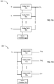
- Fig. 1A is a block diagram of a multiplexer 100A.
- the multiplexer 100A includes input terminals (In 1 ) through (In k ) (where k is an integer greater than one), analog switches 102 1 through 102 k (collectively analog switches 102), and an output terminal (Out).
- An input of each of the analog switches 102 1 through 102 k is coupled to a respective input terminal (In 1 ) through (In k ).
- An output of each of the analog switches 102 is coupled to a common terminal, e.g., the output terminal (Out).
- a switch controller 104 is coupled to control inputs of the analog switches 102 to control the state thereof.
- the switch controller 104 can turn on one of the analog switches 102, while turning off each other one of the analog switches 102. Without compensation, leakage current flowing from the output terminal (Out) through those analog switches 102 in the off-state can be significant.
- each of the analog switches 102 can be configured with buffer transistors between switch transistors and the output terminal (Out) to reduce GIDL induced in the switch transistors.
- Fig. 1B is a block diagram of a de-multiplexer 100B.
- the de-multiplexer 100B includes an input terminal (In), analog switches 102 1 through 102 m (where m is an integer greater than one), and output terminals (Out 1 ) through (Out m ).
- An input of each of the analog switches 102 is coupled to a common terminal, e.g., the input terminal (In).
- An output of each of the analog switches 102 is respectively coupled to an output terminal (Out 1 ) through (Out m ).
- the switch controller 104 is coupled to control inputs of the analog switches 102 to control the state thereof. For example, the switch controller 104 can turn on one of the analog switches 102, while turning off each other one of the analog switches 102.
- each of the analog switches 102 can be configured with buffer transistors between switch transistors and the input terminal (In) to reduce GIDL induced in the switch transistors.
- Fig. 2 is a schematic diagram showing an example analog switch 102.
- the analog switch 102 includes an n-type metal oxide semiconductor (NMOS) circuit 202 in parallel with a p-type metal oxide semiconductor (PMOS) circuit 204 between a switch input (IN) and a switch output (OUT).
- NMOS n-type metal oxide semiconductor
- PMOS p-type metal oxide semiconductor
- each of the NMOS circuit 202 and the PMOS circuit 204 includes a switch transistor and at least one buffer transistor.
- each of the NMOS circuit 202 and the PMOS circuit 204 includes both input and output buffer transistors coupled to respective source and drain of the switch transistor.
- each of the NMOS circuit 202 and the PMOS circuit 204 can include only an input buffer transistor or only an output buffer transistor.
- the NMOS circuit 202 includes a buffer transistor (MN in ), a switch transistor (MN), and a buffer transistor (MN out ).
- the transistors in the NMOS circuit 202 comprise N-channel transistors each having a substrate contact coupled to a supply voltage (Gnd).
- the supply voltage (Gnd) can be a reference voltage, such as electrical ground.
- the PMOS circuit 204 includes a buffer transistor (MP in ), a switch transistor (MP), and a buffer transistor (MP out ).
- the transistors in the PMOS circuit 204 comprise P-channel transistors each having a substrate contact coupled to a supply voltage (Vdd).
- the analog switch 102 can be fabricated using a complementary metal oxide semiconductor (CMOS) process as is known in the art.
- CMOS complementary metal oxide semiconductor
- Sources of the buffer transistors (MN in ) and (MP in ) are coupled to the switch input (IN).
- a drain of the buffer transistor (MN in ) is coupled to a source of the switch transistor (MN) (referred to as node B), and a drain of the buffer transistor (MP in ) is coupled to a source of the switch transistor (MP) (referred to as node A).
- a drain of the switch transistor (MN) is coupled to a source of the buffer transistor (MN out ) (referred to as node D), and a drain of the switch transistor (MP) is coupled to a source of the buffer transistor (MP out ) (referred to as node C). Drains of the buffer transistors (MN out ) and (MP out ) are coupled to the switch output (OUT).
- a gate of the switch transistor (MN) is coupled to receive an enable signal (EN).
- a gate of the switch transistor (MP) is coupled to receive a complement of the enable signal (EN_B).
- the enable signal is two-state signal that controls the state of the analog switch 102. If the enable signal is logic high, the analog switch 102 is on. Conversely, if the enable signal is logic low, the analog switch 102 is off.
- Gates of the buffer transistors (MN in ) and (MN out ) are coupled to receive a modulated N-channel gate voltage (NGATE).
- Gates of the buffer transistors (MP in ) and (MP out ) are coupled to receive a modulated P-channel gate voltage (PGATE).
- the analog switch 102 also includes a control circuit 208 configured to provide modulated gate voltages (NGATE) and (PGATE).
- the control circuit 208 can include a first circuit 210 and a second circuit 212.
- the first circuit 210 is configured to provide the modulated N-channel gate voltage (NGATE) for buffer transistor(s) in the NMOS circuit 202.
- the second circuit 212 is configured to provide a modulated P-channel gate voltage for buffer transistor(s) in the PMOS circuit 204.
- the first circuit 210 of the control circuit 208 comprises an N-channel transistor (MN n_off ) and a P-channel transistor (MP n _ on ). Drains of the transistors (MN n_off ) and (MP n _ on ) are coupled together to provide the modulated N-channel gate voltage (NGATE). A source of the transistor (MN n_off ) receives a GIDL mitigation voltage (V gidl ). A source of the transistor (MP n _ on ) receives the supply voltage (Vdd). Gates of the transistors (MN n_off ) and (MP n _ on ) receive the complement of the enable signal (EN_B). In Fig. 2 , NGATE refers to a common terminal such that the drains of the transistors (MN n_off ) and (MP n _ on ) are coupled to the gates of the transistors (MN in ) and (MN out ).
- the second circuit 212 of the control circuit 208 comprises an N-channel transistor (MN p_off ) and an N-channel transistor (MN p _ on ). Drains of the transistors (MN p _ off ) and (MN p _ on ) are coupled together to provide the modulated P-channel gate voltage (PGATE).
- PGATE refers to a common terminal such that the drains of the transistors (MN p_off ) and (MN p _ on ) are coupled to the gates of the transistors (MP in ) and (MP out ).
- a source of the transistor (MN p_off ) receives a GIDL mitigation voltage (V' gidl ).
- a source of the transistor (MN p_on ) receives the supply voltage (Gnd).
- Gates of the transistors (MN p _ off ) and (MN p_on ) receive the complement of the enable signal (EN_B) and the enable signal (EN), respectively.
- substrate terminals of the transistors (MN n _ off ), (MP n _ on ), (MN p _ off ), and (MN p _ on ) are coupled to the respective sources thereof.
- the substrate contacts of the NMOS devices can be coupled to the supply voltage (Gnd)
- the substrate contacts of the PMOS device can be coupled to the supply voltage (Vdd).
- Operation of the analog switch 102 can be understood with respect to the following example.
- the supply voltage (Gnd) is 0V
- the supply voltage (Vdd) is 1.8V
- the GIDL mitigation voltages (V gidl ) and (V' gidl ) are both 0.9V.
- logic low equates to the supply voltage (Gnd)
- logic high equates to the supply voltage (Vdd).
- the switch input (IN) receives an analog signal that varies between the supply voltage (Gnd) and the supply voltage (Vdd).
- the enable signal (EN) is at 1.8V and the complement of the enable signal (EN_B) is 0V.
- the transistor (MN n _ on ) is turned on, which pulls the modulated N-channel gate voltage (NGATE) to 1.8V (Vdd).
- the transistor (MP p _ on ) is turned on, which pulls the modulated P-channel gate voltage (PGATE) to 0V (Gnd).
- the analog switch 102 samples the switch input and the switch output follows the switch input.
- the enable signal (EN) is at 0V and the complement of the enable signal (EN_B) is 1.8V.
- the transistor (MN n_off ) is turned on, which pulls the modulated N-channel gate voltage (NGATE) to 0.9V (V gidl ).
- the buffer transistors (MN in ) and (MN out ) are either off or weakly on and, in either case, have high resistance between source and drain.
- the transistor (MP p _ off ) is turned on, which pulls the modulated P-channel gate voltage (PGATE) to 0.9V (V' gidl ).
- the buffer transistors (MP in ) and (MP out ) are either off or weakly on and, in either case, have high resistance between source and drain.
- the switch transistors (MN) and (MP) are off.
- Fig. 3 is a graph 300 showing NMOS leakage current versus gate voltage for the analog switch 102 in the off state.
- the graph 300 includes an axis 302 representing gate voltage of a buffer transistor in the NMOS circuit 202.
- the graph 300 includes an axis 304 representing NMOS leakage current.
- a curve 306 represents the NMOS leakage current for the conventional CMOS switch in the off state (e.g., the gate voltage is always Gnd).
- the NMOS leakage current is substantially constant in the conventional CMOS switch at a value of I leak .
- a curve 308 represents the NMOS leakage current versus gate voltage for the analog switch 102 as the gate voltage thereof varies between 0V and 2V.
- the NMOS leakage current is approximately double I leak at 0V. This assumes that the buffer transistor and the switch transistor in the NMOS circuit 202 are twice the size of the switch transistor in the conventional CMOS switch so that the on-resistance is the same between the two circuits.
- the NMOS leakage current of the analog switch 102 decreases and approaches 0.1 x I leak (ten times less than the conventional CMOS switch) (e.g., at 900 mV).
- the NMOS leakage current of the analog switch 102 begins to increase and approach Il eak .
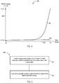
- Fig. 4 is a graph 400 showing NMOS leakage current versus drain voltage for the analog switch 102 and for a conventional CMOS switch, each in the off state.
- the graph 400 includes an axis 402 representing drain voltage.
- the "drain voltage” corresponds to the drain voltage of a buffer transistor in the NMOS circuit 202.
- the "drain voltage” corresponds to the drain voltage of the N-channel switch transistor.
- the graph 400 includes an axis 404 representing NMOS leakage current.
- a curve 406 represents NMOS leakage current for the conventional CMOS switch in the off-state (e.g., the gate voltage is GND) as the drain voltage varies between 0V and 2V.
- a curve 408 represents NMOS leakage current for the analog switch 102 as the drain voltage varies between 0V and 2V.
- the curve 408 is substantially constant across the range of drain voltage, since the GIDL current is substantially reduced as described above.
- the NMOS leakage current substantially comprises the sub-threshold leakage current.
- Fig. 5 is a flow diagram shown an example of a method 500 of operating the analog switch 102.
- a switch controller e.g., the switch controller 104 couples complementary enable signals to gates of switch transistors in the NMOS circuit 202 and the PMOS circuit 204 to control switch state of the analog switch 102.
- the control circuit 208 applies modulated gate voltages to gates of buffer transistors in the NMOS circuit 202 and the PMOS circuit 204.
- Each of the modulated gate voltages alternates between a respective supply voltage and a respective GIDL mitigation voltage.
- Modulated N-channel and modulated P-channel gate voltages can be a respective supply voltage when the switch state is on and a respective GIDL voltage when the switch state is off.
- the analog switch 102 can be used in various applications, including on various integrated circuit applications.
- the analog switch 102 can be used on a programmable integrated circuit, such as a field programmable gate array (FPGA).
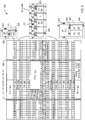
- FIG. 6 illustrates an example architecture of an FPGA 600 that includes a large number of different programmable tiles including multi-gigabit transceivers ("MGTs") 601, configurable logic blocks (“CLBs”) 602, random access memory blocks (“BRAMs”) 603, input/output blocks (“lOBs”) 604, configuration and clocking logic (“CONFIG/CLOCKS”) 605, digital signal processing blocks (“DSPs”) 606, specialized input/output blocks (“I/O”) 607 (e.g., configuration ports and clock ports), and other programmable logic 608 such as digital clock managers, analog-to-digital converters, system monitoring logic, and so forth.
- Some FPGAs also include dedicated processor blocks (“PROC”) 610.
- PROC dedicated processor blocks
- each programmable tile can include at least one programmable interconnect element ("INT") 611 having connections to input and output terminals 620 of a programmable logic element within the same tile, as shown by examples included at the top of FIG. 6 .
- Each programmable interconnect element 611 can also include connections to interconnect segments 622 of adjacent programmable interconnect element(s) in the same tile or other tile(s).
- Each programmable interconnect element 611 can also include connections to interconnect segments 624 of general routing resources between logic blocks (not shown).
- the general routing resources can include routing channels between logic blocks (not shown) comprising tracks of interconnect segments (e.g., interconnect segments 624) and switch blocks (not shown) for connecting interconnect segments.
- interconnect segments of the general routing resources can span one or more logic blocks.
- the programmable interconnect elements 611 taken together with the general routing resources implement a programmable interconnect structure ("programmable interconnect") for the illustrated FPGA.
- a CLB 602 can include a configurable logic element (“CLE”) 612 that can be programmed to implement user logic plus a single programmable interconnect element (“INT") 611.
- a BRAM 603 can include a BRAM logic element (“BRL”) 613 in addition to one or more programmable interconnect elements.
- BRAM logic element BRAM logic element
- the number of interconnect elements included in a tile depends on the height of the tile. In the pictured example, a BRAM tile has the same height as five CLBs, but other numbers (e.g., four) can also be used.
- a DSP tile 606 can include a DSP logic element (“DSPL”) 614 in addition to an appropriate number of programmable interconnect elements.
- An IOB 604 can include, for example, two instances of an input/output logic element ("IOL") 615 in addition to one instance of the programmable interconnect element 611.
- IOL input/output logic element
- the actual I/O pads connected, for example, to the I/O logic element 615 typically are not confined to the area of the input/output logic element 615.
- a horizontal area near the center of the die (shown in FIG. 6 ) is used for configuration, clock, and other control logic.
- Vertical columns 609 extending from this horizontal area or column are used to distribute the clocks and configuration signals across the breadth of the FPGA.
- Some FPGAs utilizing the architecture illustrated in FIG. 6 include additional logic blocks that disrupt the regular columnar structure making up a large part of the FPGA.
- the additional logic blocks can be programmable blocks and/or dedicated logic.
- processor block 610 spans several columns of CLBs and BRAMs.
- the processor block 610 can various components ranging from a single microprocessor to a complete programmable processing system of microprocessor(s), memory controllers, peripherals, and the like.
- FIG. 6 is intended to illustrate only an exemplary FPGA architecture.
- the numbers of logic blocks in a row, the relative width of the rows, the number and order of rows, the types of logic blocks included in the rows, the relative sizes of the logic blocks, and the interconnect/logic implementations included at the top of FIG. 6 are purely exemplary.
- more than one adjacent row of CLBs is typically included wherever the CLBs appear, to facilitate the efficient implementation of user logic, but the number of adjacent CLB rows varies with the overall size of the FPGA.
- the FPGA of FIG. 6 illustrates one example of a programmable IC that can employ examples of the interconnect circuits described herein.
- the interconnect circuits described herein can be used in other types of programmable ICs, such as complex programmable logic devices (CPLDs) or any type of programmable IC having a programmable interconnect structure for selectively coupling logic elements.
- CPLDs complex programmable logic devices
- the FPGA 600 can include analog circuits 650.
- the analog circuits 650 can include one or more analog switches 102 in various circuit configurations.
- the analog circuits 650 can include multiplexers, de-multiplexers, and the like where leakage current has a significant impact on circuit operation.
- the analog switches 102 can be employed to reduce leakage current, as described above.
- an apparatus includes an analog switch.
- the analog switch may include: an analog switch including an n-type metal oxide semiconductor (NMOS) circuit in parallel with a p-type metal oxide semiconductor (PMOS) circuit between a switch input and a switch output, the analog switch responsive to an enable signal that determines switch state thereof;
- the NMOS circuit may include a switch N-channel transistor coupled to a buffer N-channel transistor, a gate of the switch N-channel transistor coupled to the enable signal and a gate of the buffer N-channel transistor coupled to a modulated N-channel gate voltage;
- the PMOS circuit including a switch P-channel transistor coupled to a buffer P-channel transistor, a gate of the switch P-channel transistor coupled to a complement of the enable signal and a gate of the buffer P-channel transistor coupled to a modulated P-channel gate voltage; and a control circuit coupled to the analog switch to provide the modulated N-channel and modulated P-channel gate voltages each of which alternates between a respective supply voltage and a respective gate induced drain leakage (
- each of the modulated N-channel and modulated P-channel gate voltages may be a respective supply voltage when the switch state is on and a respective GIDL mitigation voltage when the switch state is off.
- the modulated N-channel gate voltage may alternate between a respective supply voltage being a first supply voltage and a respective GIDL mitigation voltage being a first GIDL mitigation voltage; and the modulated P-channel gate voltage may alternate between a respective supply voltage being a second supply voltage and a respective GIDL mitigation voltage being a second GIDL mitigation voltage.
- the first supply voltage may include a positive voltage and the second supply voltage may include a reference voltage, and the first and second GIDL mitigation voltages may be between the positive voltage and the reference voltage.
- each of the first and second GIDL mitigation voltages may be approximately equal to half of the difference between the positive voltage and the reference voltage.
- control circuit may include: a first circuit coupled to apply the modulated N-channel gate voltage to the gate of the buffer N-channel transistor; and a second circuit coupled to apply the modulated P-channel gate voltage to the gate of the buffer P-channel transistor.
- the first circuit may include: an N-channel transistor having a source coupled to the first GIDL mitigation voltage, a drain coupled to the gate of the buffer N-channel transistor, and a gate coupled to the complement of the enable signal; and a P-channel transistor having a source coupled to the first supply voltage, a drain coupled to the gate of the buffer N-channel transistor, and a gate coupled to the complement of the enable signal.
- the second circuit may include: a first N-channel transistor having a source coupled to the second GIDL mitigation voltage, a drain coupled to the gate of the buffer P-channel transistor, and a gate coupled to the complement of the enable signal; and a second N-channel transistor having a source coupled to the second supply voltage, a drain coupled to the gate of the buffer P-channel transistor, and a gate coupled to the enable signal.
- the buffer N-channel transistor and the buffer P-channel transistor may be coupled between the switch output and respective drains of the switch N-channel transistor and the switch P-channel transistor.
- the buffer N-channel transistor and the buffer P-channel transistor may be coupled between the switch input and respective sources of the switch N-channel transistor and the switch P-channel transistor.
- the buffer N-channel transistor may include an input buffer N-channel transistor and the buffer P-channel transistor may include an input buffer P-channel transistor;
- the NMOS circuit may include an output buffer N-channel transistor coupled between the switch output and a drain of the switch N-channel transistor, a gate of the output buffer N-channel transistor coupled to the modulated N-channel gate voltage;
- the PMOS circuit may include an output buffer P-channel transistor coupled between the switch output and a drain of the switch P-channel transistor, a gate of the output buffer P-channel transistor coupled to the modulated P-channel gate voltage.
- an apparatus may include: a plurality of analog switches coupled to a common terminal, each of the plurality of analog switches responsive to a respective enable signal that determines switch state thereof, each of the plurality of analog switches may include: an n-type metal oxide semiconductor (NMOS) circuit in parallel with a p-type metal oxide semiconductor (PMOS) circuit between a switch input and a switch output; the NMOS circuit including a switch N-channel transistor coupled to a buffer N-channel transistor, a gate of the switch N-channel transistor coupled to the respective enable signal and a gate of the buffer N-channel transistor coupled to a modulated N-channel gate voltage; the PMOS circuit including a switch P-channel transistor coupled to a buffer P-channel transistor, a gate of the switch P-channel transistor coupled to a complement of the respective enable signal and a gate of the buffer P-channel transistor coupled to a modulated P-channel gate voltage; and a control circuit coupled to NMOS and PMOS circuits to provide the modulated N-channel and modulated P-channel gate voltage
- each of the modulated N-channel and modulated P-channel gate voltages is a respective supply voltage when the switch state is on and a respective GIDL mitigation voltage when the switch state is off.
- the modulated N-channel gate voltage alternates between a respective supply voltage being a first supply voltage and a respective GIDL mitigation voltage being a first GIDL mitigation voltage; and the modulated P-channel gate voltage alternates between a respective supply voltage being a second supply voltage and a respective GIDL mitigation voltage being a second GIDL mitigation voltage.
- the first supply voltage may include a positive voltage and the second supply voltage may include a reference voltage, and wherein the first and second GIDL mitigation voltages are between the positive voltage and the reference voltage.
- the control circuit may include: a first circuit coupled to apply the modulated N-channel gate voltage to the gate of the buffer N-channel transistor, the first circuit including: an N-channel transistor having a source coupled to the first GIDL mitigation voltage, a drain coupled to the gate of the buffer N-channel transistor, and a gate coupled to the complement of the enable signal; and a P-channel transistor having a source coupled to the first supply voltage, a drain coupled to the gate of the buffer N-channel transistor, and a gate coupled to the complement of the enable signal; and a second circuit coupled to apply the modulated P-channel gate voltage to the gate of the buffer P-channel transistor, the second circuit including: a first N-channel transistor having a source coupled to the second GIDL mitigation voltage, a drain coupled to the gate of the buffer P-channel transistor, and a gate coupled to the complement of the enable signal; and a second N-channel transistor having a source coupled to the second supply voltage, a drain coupled to the gate of the buffer P-channel transistor, and a gate coupled to the complement of
- a method of operating an analog switch may include an n-type metal oxide semiconductor (NMOS) circuit in parallel with a p-type metal oxide semiconductor (PMOS) circuit between a switch input and a switch output, the method may include: coupling complementary enable signals to gates of switch transistors of the NMOS and PMOS circuits to control switch state of the analog switch; and applying modulated gate voltages to gates of buffer transistors of the NMOS and PMOS circuits, each of the modulated gate voltages alternating between a respective supply voltage and a respective gate induced drain leaking (GIDL) mitigation voltage based on the switch state.
- NMOS n-type metal oxide semiconductor
- PMOS p-type metal oxide semiconductor
- the analog switch is one of a plurality of analog switches coupled to a common terminal, and the buffer transistors are coupled between the switch transistors and the common terminal.
- each of the modulated gate voltages is a respective supply voltage when the switch state is on and a respective GIDL mitigation voltage when the switch state is off.
Landscapes
- Electronic Switches (AREA)
- Design And Manufacture Of Integrated Circuits (AREA)
Claims (14)
- Appareil (100), comprenant:un commutateur analogique (102) qui inclut un circuit métal-oxyde-semiconducteur de type n, NMOS, (202) en parallèle avec un circuit métal-oxyde-semiconducteur de type p, PMOS, (204) entre une entrée de commutation (In) et une sortie de commutation (Out), le commutateur analogique (102) étant sensible à un signal de validation (EN) qui détermine son état de commutation ;le circuit NMOS (202) incluant un transistor à canal N de commutation (MN) qui est couplé entre l'entrée de commutation (In) ou la sortie de commutation (Out) et une source ou un drain d'un transistor à canal N tampon (MNin, MNout), une grille du transistor à canal N de commutation (MN) étant couplée au signal de validation (EN) et une grille du transistor à canal N tampon (MNin, MNout) étant couplée à une tension de grille de canal N modulée (NGATE) ;le circuit PMOS (204) incluant un transistor à canal P de commutation (MP) qui est couplé entre l'entrée de commutation (In) ou la sortie de commutation (Out) et une source ou un drain d'un transistor à canal P tampon (MPin, MPout), une grille du transistor à canal P de commutation (MP) étant couplée à un complément (EN_B) du signal de validation (EN) et une grille du transistor à canal P tampon (MPin, MPout) étant couplée à une tension de grille de canal P modulée (PGATE) ; etun circuit de commande (208) qui est couplé au commutateur analogique (102) et qui reçoit le signal de validation (EN), le circuit de commande (208) étant configuré de manière à ce qu'il fournisse les tensions de grille de canal N modulée et de grille de canal P modulée (NGATE, PGATE) dont chacune réalise une alternance entre une tension d'alimentation respective (Vdd, Gnd) et une tension de limitation de fuite de drain induite par grille, GIDL, respective (Vgidl, V'gidl) sur la base de l'état du signal de validation (EN).
- Appareil (100) selon la revendication 1, dans lequel chacune des tensions de grille de canal N modulée et de grille de canal P modulée (NGATE, PGATE) est une tension d'alimentation respective (Vdd, Gnd) lorsque l'état de commutation est l'activation et est une tension de limitation de GIDL respective (Vgidl, V'gidl) lorsque l'état de commutation est la désactivation.
- Appareil (100) selon la revendication 2, dans lequel :la tension de grille de canal N modulée (NGATE) réalise une alternance entre une tension d'alimentation respective (Vdd) qui est une première tension d'alimentation et une tension de limitation de GIDL respective (Vgidl) qui est une première tension de limitation de GIDL ; etla tension de grille de canal P modulée (PGATE) réalise une alternance entre une tension d'alimentation respective (Gnd) qui est une seconde tension d'alimentation et une tension de limitation de GIDL respective (V'gidl) qui est une seconde tension de limitation de GIDL.
- Appareil (100) selon la revendication 3, dans lequel la première tension d'alimentation (Vdd) comprend une tension positive et la seconde tension d'alimentation (Gnd) comprend une tension de référence, et dans lequel les première et seconde tensions de limitation de GIDL (Vgidl, V'gidl) sont entre la tension positive et la tension de référence.
- Appareil (100) selon la revendication 4, dans lequel chacune des première et seconde tensions de limitation de GIDL (Vgidl, V'gidl) est égale à la moitié de la différence entre la tension positive et la tension de référence.
- Appareil (100) selon l'une quelconque des revendications 1 à 5, dans lequel le circuit de commande (208) comprend :un premier circuit (210) qui est couplé de manière à ce qu'il applique la tension de grille de canal N modulée (NGATE) sur la grille du transistor à canal N tampon (MNin, MNout) ; etun second circuit (212) qui est couplé de manière à ce qu'il applique la tension de grille de canal P modulée (PGATE) sur la grille du transistor à canal P tampon (MPin, MPout).
- Appareil (100) selon la revendication 6, dans lequel le premier circuit (210) comprend :un transistor à canal N (MNn_off) qui comporte une source qui est couplée à la première tension de limitation de GIDL (Vgidl), un drain qui est couplé à la grille du transistor à canal N tampon (MNin, MNout) et une grille qui est couplée au complément (EN_B) du signal de validation (EN) ; etun transistor à canal P (MPn_on) qui comporte une source qui est couplée à la première tension d'alimentation (Vdd), un drain qui est couplé à la grille du transistor à canal N tampon (MNin, MNout) et une grille qui est couplée au complément (EN_B) du signal de validation (EN).
- Appareil (100) selon la revendication 6, dans lequel le second circuit (212) comprend :un premier transistor à canal N (MNp_off) qui comporte une source qui est couplée à la seconde tension de limitation de GIDL (V'gidl), un drain qui est couplé à la grille du transistor à canal P tampon (MPin, MPout) et une grille qui est couplée au complément (EN_B) du signal de validation (EN) ; etun second transistor à canal N (MNp_on) qui comporte une source qui est couplée à la seconde tension d'alimentation (Gnd), un drain qui est couplé à la grille du transistor à canal P tampon (MPin, MPout) et une grille qui est couplée au signal de validation (EN).
- Appareil (100) selon l'une quelconque des revendications 1 à 8, dans lequel le transistor à canal N tampon (MNout) et le transistor à canal P tampon (MPout) sont couplés entre la sortie de commutation (Out) et les drains respectifs du transistor à canal N de commutation (MN) et du transistor à canal P de commutation (MP).
- Appareil (100) selon l'une quelconque des revendications 1 à 8, dans lequel le transistor à canal N tampon (MNin) et le transistor à canal P tampon (MPin) sont couplés entre l'entrée de commutation (In) et les sources respectives du transistor à canal N de commutation (MN) et du transistor à canal P de commutation (MP).
- Appareil selon la revendication 10, dans lequel :le transistor à canal N tampon (MNin, MNout) comprend un transistor à canal N tampon d'entrée (MNin) et le transistor à canal P tampon (MPin, MPout) comprend un transistor à canal P tampon d'entrée (MPin) ;le circuit NMOS (202) inclut un transistor à canal N tampon de sortie (MNout) qui est couplé entre la sortie de commutation (Out) et un drain du transistor à canal N de commutation (MN), une grille du transistor à canal N tampon de sortie (MNout) étant couplée à la tension de grille de canal N modulée (NGATE) ; etle circuit PMOS (204) inclut un transistor à canal P tampon de sortie (MPout) qui est couplé entre la sortie de commutation (Out) et un drain du transistor à canal P de commutation (MP), une grille du transistor à canal P tampon de sortie (MPout) étant couplée à la tension de grille de canal P modulée (PGATE).
- Procédé de fonctionnement d'un commutateur analogique (102) qui comprend un circuit métal-oxyde-semiconducteur de type n, NMOS, (202) en parallèle avec un circuit métal-oxyde-semiconducteur de type p, PMOS, (204) entre une entrée de commutation (In) et une sortie de commutation (Out), le procédé comprenant :le couplage de signaux de validation complémentaires (EN, EN_B) sur des grilles de transistors de commutation (MN, MP) des circuits NMOS et PMOS (202, 204) de manière à commander l'état de commutation du commutateur analogique (102), les transistors de commutation (MN, MP) étant couplés entre l'entrée de commutation (In) ou la sortie de commutation (Out) et des sources ou des drains de transistors tampon (MNin, MNout, MPin, MPout) des circuits NMOS et PMOS (202, 204) ; etl'application de tensions de grille modulées (NGATE, PGATE) sur des grilles des transistors tampon (MNin, MNout, MPin, MPout) des circuits NMOS et PMOS (202, 204), chacune des tensions de grille modulées (NGATE, PGATE) réalisant une alternance entre une tension d'alimentation respective (Vdd, Gnd) et une tension de limitation de fuite de drain induite par grille, GIDL, respective (Vgidl, V'gidl) sur la base des signaux de validation complémentaires (EN, EN_B).
- Procédé selon la revendication 12, dans lequel le commutateur analogique (102) est l'un d'une pluralité de commutateurs analogiques (102l-102k, 102m) qui sont couplés à une borne commune (In, Out), et les transistors tampon (MNin, MNout, MPin, MPout) sont couplés entre les transistors de commutation (MN, MP) et la borne commune (In, Out).
- Procédé selon la revendication 13, dans lequel chacune des tensions de grille modulées (NGATE, PGATE) est une tension d'alimentation respective (Vdd, Gnd) lorsque l'état de commutation est l'activation et est une tension de limitation de GIDL respective (Vgidl, V'gidl) lorsque l'état de commutation est la désactivation.
Applications Claiming Priority (2)
| Application Number | Priority Date | Filing Date | Title |
|---|---|---|---|
| US14/659,747 US10236873B2 (en) | 2015-03-17 | 2015-03-17 | Analog switch having reduced gate-induced drain leakage |
| PCT/US2016/022505 WO2016149290A1 (fr) | 2015-03-17 | 2016-03-15 | Commutateur analogique à fuite de drain induite par la grille réduite |
Publications (2)
| Publication Number | Publication Date |
|---|---|
| EP3272011A1 EP3272011A1 (fr) | 2018-01-24 |
| EP3272011B1 true EP3272011B1 (fr) | 2019-06-26 |
Family
ID=55629136
Family Applications (1)
| Application Number | Title | Priority Date | Filing Date |
|---|---|---|---|
| EP16711958.5A Active EP3272011B1 (fr) | 2015-03-17 | 2016-03-15 | Commutateur analogique à fuite de drain induite par la grille réduite |
Country Status (6)
| Country | Link |
|---|---|
| US (1) | US10236873B2 (fr) |
| EP (1) | EP3272011B1 (fr) |
| JP (1) | JP6686038B2 (fr) |
| KR (1) | KR102499454B1 (fr) |
| CN (1) | CN107408940B (fr) |
| WO (1) | WO2016149290A1 (fr) |
Families Citing this family (16)
| Publication number | Priority date | Publication date | Assignee | Title |
|---|---|---|---|---|
| US10033396B1 (en) | 2017-03-26 | 2018-07-24 | Nxp Usa, Inc. | Active switch having low leakage current |
| US9673831B1 (en) | 2017-03-26 | 2017-06-06 | Nxp Usa, Inc. | Passive switch having low leakage current |
| US10545053B2 (en) * | 2017-06-07 | 2020-01-28 | Xilinx, Inc. | Dynamic element matching in an integrated circuit |
| US20190020273A1 (en) * | 2017-07-17 | 2019-01-17 | Nanya Technology Corporation | Voltage system and method for operating the same |
| US10522542B1 (en) | 2018-06-28 | 2019-12-31 | Taiwan Semiconductor Manufacturing Co., Ltd. | Double rule integrated circuit layouts for a dual transmission gate |
| US10454476B2 (en) * | 2018-09-28 | 2019-10-22 | Intel Corporation | Calibrated biasing of sleep transistor in integrated circuits |
| US10972096B2 (en) * | 2019-06-28 | 2021-04-06 | Nxp Usa, Inc. | Electronic switch |
| US11237580B1 (en) * | 2020-09-09 | 2022-02-01 | Qualcomm Incorporated | Systems and methods providing leakage reduction for power gated domains |
| US11190178B1 (en) | 2020-10-28 | 2021-11-30 | Xilinx, Inc. | Gate induced drain leakage robust bootstrapped switch |
| CN115514356A (zh) | 2021-06-23 | 2022-12-23 | 恩智浦美国有限公司 | 模拟开关布置 |
| US12132476B2 (en) | 2021-07-07 | 2024-10-29 | Samsung Electro-Mechanics Co., Ltd. | Power supply switch circuit and operating method thereof |
| JP7682822B2 (ja) * | 2022-03-15 | 2025-05-26 | 株式会社東芝 | アナログスイッチ回路 |
| US11894840B2 (en) * | 2022-04-01 | 2024-02-06 | Psemi Corporation | Output buffer for a swappable single conductor interface |
| WO2024075785A1 (fr) * | 2022-10-07 | 2024-04-11 | 東京エレクトロン株式会社 | Dispositif de traitement de substrat et mandrin électrostatique |
| US12113520B2 (en) | 2022-12-22 | 2024-10-08 | Nxp B.V. | Circuit to reduce gate induced drain leakage |
| CN116682371A (zh) * | 2023-06-27 | 2023-09-01 | 上海天马微电子有限公司 | 显示面板及显示装置 |
Family Cites Families (8)
| Publication number | Priority date | Publication date | Assignee | Title |
|---|---|---|---|---|
| JPS60174518A (ja) * | 1984-02-20 | 1985-09-07 | Hitachi Ltd | Cmosアナログスイツチ |
| JP3688497B2 (ja) * | 1999-02-17 | 2005-08-31 | 株式会社東芝 | アナログスイッチ回路 |
| JP2003229748A (ja) * | 2002-02-04 | 2003-08-15 | Matsushita Electric Ind Co Ltd | アナログスイッチ回路 |
| JP3983220B2 (ja) * | 2003-12-24 | 2007-09-26 | 沖電気工業株式会社 | アナログスイッチ |
| JP4832965B2 (ja) * | 2006-06-07 | 2011-12-07 | パナソニック株式会社 | スイッチ回路装置、スイッチ回路装置を用いた無線回路装置及びサンプリング回路装置 |
| US8228109B2 (en) * | 2010-06-28 | 2012-07-24 | Freescale Semiconductor, Inc. | Transmission gate circuitry for high voltage terminal |
| JP5845112B2 (ja) * | 2012-02-29 | 2016-01-20 | セイコーインスツル株式会社 | スイッチ回路 |
| US9245886B2 (en) | 2013-07-12 | 2016-01-26 | Xilinx, Inc. | Switch supporting voltages greater than supply |
-
2015
- 2015-03-17 US US14/659,747 patent/US10236873B2/en active Active
-
2016
- 2016-03-15 KR KR1020177029720A patent/KR102499454B1/ko active Active
- 2016-03-15 WO PCT/US2016/022505 patent/WO2016149290A1/fr not_active Ceased
- 2016-03-15 JP JP2017548923A patent/JP6686038B2/ja not_active Expired - Fee Related
- 2016-03-15 EP EP16711958.5A patent/EP3272011B1/fr active Active
- 2016-03-15 CN CN201680016468.7A patent/CN107408940B/zh active Active
Non-Patent Citations (1)
| Title |
|---|
| None * |
Also Published As
| Publication number | Publication date |
|---|---|
| CN107408940A (zh) | 2017-11-28 |
| KR102499454B1 (ko) | 2023-02-13 |
| WO2016149290A1 (fr) | 2016-09-22 |
| KR20170128529A (ko) | 2017-11-22 |
| CN107408940B (zh) | 2021-01-05 |
| US20160277019A1 (en) | 2016-09-22 |
| US10236873B2 (en) | 2019-03-19 |
| EP3272011A1 (fr) | 2018-01-24 |
| JP6686038B2 (ja) | 2020-04-22 |
| JP2018511998A (ja) | 2018-04-26 |
Similar Documents
| Publication | Publication Date | Title |
|---|---|---|
| EP3272011B1 (fr) | Commutateur analogique à fuite de drain induite par la grille réduite | |
| EP2560284B1 (fr) | Appareil pour améliorer les performances de réseaux de portes à champ programmable et procédés associés | |
| US8896363B2 (en) | Analog switching circuit, associated control circuit and method | |
| US7755392B1 (en) | Level shift circuit without high voltage stress of transistors and operating at low voltages | |
| US9407266B2 (en) | Programmable single-supply level-shifter circuit | |
| US9628081B2 (en) | Interconnect circuits having low threshold voltage P-channel transistors for a programmable integrated circuit | |
| US20180212600A1 (en) | Bidirectional Integrated CMOS Switch | |
| US20160036434A1 (en) | Semiconductor integrated circuit device | |
| EP3201639B1 (fr) | Caractérisation de transistor à puce dans un circuit intégré | |
| TW201334415A (zh) | 三態閘 | |
| CN107508593B (zh) | 具有背栅极切换的半导体结构 | |
| US8836027B2 (en) | Switch circuit using LDMOS element | |
| US10263622B2 (en) | Semiconductor apparatus and method of controlling MOS transistor | |
| US9385703B2 (en) | Circuit and method for body biasing | |
| CN112689959A (zh) | 一种传输门电路、矩阵开关以及电子设备 | |
| US9166047B2 (en) | Switch circuit using LDMOS device | |
| US20060181313A1 (en) | Transistor logic circuit | |
| JP2004032251A (ja) | アナログスイッチ | |
| KR20160099360A (ko) | 스위치 및 스위치 보호 방법 | |
| JP2006196790A (ja) | 半導体集積回路 |
Legal Events
| Date | Code | Title | Description |
|---|---|---|---|
| STAA | Information on the status of an ep patent application or granted ep patent |
Free format text: STATUS: THE INTERNATIONAL PUBLICATION HAS BEEN MADE |
|
| PUAI | Public reference made under article 153(3) epc to a published international application that has entered the european phase |
Free format text: ORIGINAL CODE: 0009012 |
|
| STAA | Information on the status of an ep patent application or granted ep patent |
Free format text: STATUS: REQUEST FOR EXAMINATION WAS MADE |
|
| 17P | Request for examination filed |
Effective date: 20170830 |
|
| AK | Designated contracting states |
Kind code of ref document: A1 Designated state(s): AL AT BE BG CH CY CZ DE DK EE ES FI FR GB GR HR HU IE IS IT LI LT LU LV MC MK MT NL NO PL PT RO RS SE SI SK SM TR |
|
| AX | Request for extension of the european patent |
Extension state: BA ME |
|
| DAV | Request for validation of the european patent (deleted) | ||
| DAX | Request for extension of the european patent (deleted) | ||
| GRAP | Despatch of communication of intention to grant a patent |
Free format text: ORIGINAL CODE: EPIDOSNIGR1 |
|
| STAA | Information on the status of an ep patent application or granted ep patent |
Free format text: STATUS: GRANT OF PATENT IS INTENDED |
|
| INTG | Intention to grant announced |
Effective date: 20190308 |
|
| RIN1 | Information on inventor provided before grant (corrected) |
Inventor name: JENNINGS, JOHN K. Inventor name: DURBHA, CHANDRIKA Inventor name: CICAL, IONUT C. |
|
| GRAS | Grant fee paid |
Free format text: ORIGINAL CODE: EPIDOSNIGR3 |
|
| GRAA | (expected) grant |
Free format text: ORIGINAL CODE: 0009210 |
|
| STAA | Information on the status of an ep patent application or granted ep patent |
Free format text: STATUS: THE PATENT HAS BEEN GRANTED |
|
| AK | Designated contracting states |
Kind code of ref document: B1 Designated state(s): AL AT BE BG CH CY CZ DE DK EE ES FI FR GB GR HR HU IE IS IT LI LT LU LV MC MK MT NL NO PL PT RO RS SE SI SK SM TR |
|
| REG | Reference to a national code |
Ref country code: GB Ref legal event code: FG4D |
|
| REG | Reference to a national code |
Ref country code: CH Ref legal event code: EP |
|
| REG | Reference to a national code |
Ref country code: AT Ref legal event code: REF Ref document number: 1149471 Country of ref document: AT Kind code of ref document: T Effective date: 20190715 |
|
| REG | Reference to a national code |
Ref country code: DE Ref legal event code: R096 Ref document number: 602016015903 Country of ref document: DE |
|
| REG | Reference to a national code |
Ref country code: IE Ref legal event code: FG4D |
|
| REG | Reference to a national code |
Ref country code: NL Ref legal event code: MP Effective date: 20190626 |
|
| PG25 | Lapsed in a contracting state [announced via postgrant information from national office to epo] |
Ref country code: HR Free format text: LAPSE BECAUSE OF FAILURE TO SUBMIT A TRANSLATION OF THE DESCRIPTION OR TO PAY THE FEE WITHIN THE PRESCRIBED TIME-LIMIT Effective date: 20190626 Ref country code: LT Free format text: LAPSE BECAUSE OF FAILURE TO SUBMIT A TRANSLATION OF THE DESCRIPTION OR TO PAY THE FEE WITHIN THE PRESCRIBED TIME-LIMIT Effective date: 20190626 Ref country code: SE Free format text: LAPSE BECAUSE OF FAILURE TO SUBMIT A TRANSLATION OF THE DESCRIPTION OR TO PAY THE FEE WITHIN THE PRESCRIBED TIME-LIMIT Effective date: 20190626 Ref country code: FI Free format text: LAPSE BECAUSE OF FAILURE TO SUBMIT A TRANSLATION OF THE DESCRIPTION OR TO PAY THE FEE WITHIN THE PRESCRIBED TIME-LIMIT Effective date: 20190626 Ref country code: AL Free format text: LAPSE BECAUSE OF FAILURE TO SUBMIT A TRANSLATION OF THE DESCRIPTION OR TO PAY THE FEE WITHIN THE PRESCRIBED TIME-LIMIT Effective date: 20190626 Ref country code: NO Free format text: LAPSE BECAUSE OF FAILURE TO SUBMIT A TRANSLATION OF THE DESCRIPTION OR TO PAY THE FEE WITHIN THE PRESCRIBED TIME-LIMIT Effective date: 20190926 |
|
| REG | Reference to a national code |
Ref country code: LT Ref legal event code: MG4D |
|
| PG25 | Lapsed in a contracting state [announced via postgrant information from national office to epo] |
Ref country code: BG Free format text: LAPSE BECAUSE OF FAILURE TO SUBMIT A TRANSLATION OF THE DESCRIPTION OR TO PAY THE FEE WITHIN THE PRESCRIBED TIME-LIMIT Effective date: 20190926 Ref country code: GR Free format text: LAPSE BECAUSE OF FAILURE TO SUBMIT A TRANSLATION OF THE DESCRIPTION OR TO PAY THE FEE WITHIN THE PRESCRIBED TIME-LIMIT Effective date: 20190927 Ref country code: LV Free format text: LAPSE BECAUSE OF FAILURE TO SUBMIT A TRANSLATION OF THE DESCRIPTION OR TO PAY THE FEE WITHIN THE PRESCRIBED TIME-LIMIT Effective date: 20190626 Ref country code: RS Free format text: LAPSE BECAUSE OF FAILURE TO SUBMIT A TRANSLATION OF THE DESCRIPTION OR TO PAY THE FEE WITHIN THE PRESCRIBED TIME-LIMIT Effective date: 20190626 |
|
| REG | Reference to a national code |
Ref country code: AT Ref legal event code: MK05 Ref document number: 1149471 Country of ref document: AT Kind code of ref document: T Effective date: 20190626 |
|
| PG25 | Lapsed in a contracting state [announced via postgrant information from national office to epo] |
Ref country code: EE Free format text: LAPSE BECAUSE OF FAILURE TO SUBMIT A TRANSLATION OF THE DESCRIPTION OR TO PAY THE FEE WITHIN THE PRESCRIBED TIME-LIMIT Effective date: 20190626 Ref country code: AT Free format text: LAPSE BECAUSE OF FAILURE TO SUBMIT A TRANSLATION OF THE DESCRIPTION OR TO PAY THE FEE WITHIN THE PRESCRIBED TIME-LIMIT Effective date: 20190626 Ref country code: CZ Free format text: LAPSE BECAUSE OF FAILURE TO SUBMIT A TRANSLATION OF THE DESCRIPTION OR TO PAY THE FEE WITHIN THE PRESCRIBED TIME-LIMIT Effective date: 20190626 Ref country code: NL Free format text: LAPSE BECAUSE OF FAILURE TO SUBMIT A TRANSLATION OF THE DESCRIPTION OR TO PAY THE FEE WITHIN THE PRESCRIBED TIME-LIMIT Effective date: 20190626 Ref country code: RO Free format text: LAPSE BECAUSE OF FAILURE TO SUBMIT A TRANSLATION OF THE DESCRIPTION OR TO PAY THE FEE WITHIN THE PRESCRIBED TIME-LIMIT Effective date: 20190626 Ref country code: PT Free format text: LAPSE BECAUSE OF FAILURE TO SUBMIT A TRANSLATION OF THE DESCRIPTION OR TO PAY THE FEE WITHIN THE PRESCRIBED TIME-LIMIT Effective date: 20191028 Ref country code: SK Free format text: LAPSE BECAUSE OF FAILURE TO SUBMIT A TRANSLATION OF THE DESCRIPTION OR TO PAY THE FEE WITHIN THE PRESCRIBED TIME-LIMIT Effective date: 20190626 |
|
| PG25 | Lapsed in a contracting state [announced via postgrant information from national office to epo] |
Ref country code: IT Free format text: LAPSE BECAUSE OF FAILURE TO SUBMIT A TRANSLATION OF THE DESCRIPTION OR TO PAY THE FEE WITHIN THE PRESCRIBED TIME-LIMIT Effective date: 20190626 Ref country code: IS Free format text: LAPSE BECAUSE OF FAILURE TO SUBMIT A TRANSLATION OF THE DESCRIPTION OR TO PAY THE FEE WITHIN THE PRESCRIBED TIME-LIMIT Effective date: 20191026 Ref country code: SM Free format text: LAPSE BECAUSE OF FAILURE TO SUBMIT A TRANSLATION OF THE DESCRIPTION OR TO PAY THE FEE WITHIN THE PRESCRIBED TIME-LIMIT Effective date: 20190626 |
|
| PG25 | Lapsed in a contracting state [announced via postgrant information from national office to epo] |
Ref country code: TR Free format text: LAPSE BECAUSE OF FAILURE TO SUBMIT A TRANSLATION OF THE DESCRIPTION OR TO PAY THE FEE WITHIN THE PRESCRIBED TIME-LIMIT Effective date: 20190626 |
|
| PG25 | Lapsed in a contracting state [announced via postgrant information from national office to epo] |
Ref country code: DK Free format text: LAPSE BECAUSE OF FAILURE TO SUBMIT A TRANSLATION OF THE DESCRIPTION OR TO PAY THE FEE WITHIN THE PRESCRIBED TIME-LIMIT Effective date: 20190626 Ref country code: PL Free format text: LAPSE BECAUSE OF FAILURE TO SUBMIT A TRANSLATION OF THE DESCRIPTION OR TO PAY THE FEE WITHIN THE PRESCRIBED TIME-LIMIT Effective date: 20190626 |
|
| PG25 | Lapsed in a contracting state [announced via postgrant information from national office to epo] |
Ref country code: IS Free format text: LAPSE BECAUSE OF FAILURE TO SUBMIT A TRANSLATION OF THE DESCRIPTION OR TO PAY THE FEE WITHIN THE PRESCRIBED TIME-LIMIT Effective date: 20200224 |
|
| REG | Reference to a national code |
Ref country code: DE Ref legal event code: R097 Ref document number: 602016015903 Country of ref document: DE |
|
| PLBE | No opposition filed within time limit |
Free format text: ORIGINAL CODE: 0009261 |
|
| STAA | Information on the status of an ep patent application or granted ep patent |
Free format text: STATUS: NO OPPOSITION FILED WITHIN TIME LIMIT |
|
| PG2D | Information on lapse in contracting state deleted |
Ref country code: IS |
|
| 26N | No opposition filed |
Effective date: 20200603 |
|
| PG25 | Lapsed in a contracting state [announced via postgrant information from national office to epo] |
Ref country code: SI Free format text: LAPSE BECAUSE OF FAILURE TO SUBMIT A TRANSLATION OF THE DESCRIPTION OR TO PAY THE FEE WITHIN THE PRESCRIBED TIME-LIMIT Effective date: 20190626 |
|
| PG25 | Lapsed in a contracting state [announced via postgrant information from national office to epo] |
Ref country code: ES Free format text: LAPSE BECAUSE OF FAILURE TO SUBMIT A TRANSLATION OF THE DESCRIPTION OR TO PAY THE FEE WITHIN THE PRESCRIBED TIME-LIMIT Effective date: 20190626 Ref country code: MC Free format text: LAPSE BECAUSE OF FAILURE TO SUBMIT A TRANSLATION OF THE DESCRIPTION OR TO PAY THE FEE WITHIN THE PRESCRIBED TIME-LIMIT Effective date: 20190626 |
|
| REG | Reference to a national code |
Ref country code: CH Ref legal event code: PL |
|
| REG | Reference to a national code |
Ref country code: BE Ref legal event code: MM Effective date: 20200331 |
|
| PG25 | Lapsed in a contracting state [announced via postgrant information from national office to epo] |
Ref country code: LU Free format text: LAPSE BECAUSE OF NON-PAYMENT OF DUE FEES Effective date: 20200315 |
|
| PG25 | Lapsed in a contracting state [announced via postgrant information from national office to epo] |
Ref country code: LI Free format text: LAPSE BECAUSE OF NON-PAYMENT OF DUE FEES Effective date: 20200331 Ref country code: CH Free format text: LAPSE BECAUSE OF NON-PAYMENT OF DUE FEES Effective date: 20200331 |
|
| PG25 | Lapsed in a contracting state [announced via postgrant information from national office to epo] |
Ref country code: BE Free format text: LAPSE BECAUSE OF NON-PAYMENT OF DUE FEES Effective date: 20200331 |
|
| PG25 | Lapsed in a contracting state [announced via postgrant information from national office to epo] |
Ref country code: MT Free format text: LAPSE BECAUSE OF FAILURE TO SUBMIT A TRANSLATION OF THE DESCRIPTION OR TO PAY THE FEE WITHIN THE PRESCRIBED TIME-LIMIT Effective date: 20190626 Ref country code: CY Free format text: LAPSE BECAUSE OF FAILURE TO SUBMIT A TRANSLATION OF THE DESCRIPTION OR TO PAY THE FEE WITHIN THE PRESCRIBED TIME-LIMIT Effective date: 20190626 |
|
| PG25 | Lapsed in a contracting state [announced via postgrant information from national office to epo] |
Ref country code: MK Free format text: LAPSE BECAUSE OF FAILURE TO SUBMIT A TRANSLATION OF THE DESCRIPTION OR TO PAY THE FEE WITHIN THE PRESCRIBED TIME-LIMIT Effective date: 20190626 |
|
| P01 | Opt-out of the competence of the unified patent court (upc) registered |
Effective date: 20230530 |
|
| PGFP | Annual fee paid to national office [announced via postgrant information from national office to epo] |
Ref country code: GB Payment date: 20260304 Year of fee payment: 11 |
|
| PGFP | Annual fee paid to national office [announced via postgrant information from national office to epo] |
Ref country code: DE Payment date: 20260217 Year of fee payment: 11 Ref country code: IE Payment date: 20260309 Year of fee payment: 11 |
|
| PGFP | Annual fee paid to national office [announced via postgrant information from national office to epo] |
Ref country code: FR Payment date: 20260302 Year of fee payment: 11 |