EP3264471A1 - Verbesserte epi-integralität auf source-/drain-bereichen von finfet - Google Patents
Verbesserte epi-integralität auf source-/drain-bereichen von finfet Download PDFInfo
- Publication number
- EP3264471A1 EP3264471A1 EP17178152.9A EP17178152A EP3264471A1 EP 3264471 A1 EP3264471 A1 EP 3264471A1 EP 17178152 A EP17178152 A EP 17178152A EP 3264471 A1 EP3264471 A1 EP 3264471A1
- Authority
- EP
- European Patent Office
- Prior art keywords
- gate
- semiconductor fin
- trench isolation
- layer
- insulator layer
- Prior art date
- Legal status (The legal status is an assumption and is not a legal conclusion. Google has not performed a legal analysis and makes no representation as to the accuracy of the status listed.)
- Withdrawn
Links
Images






Classifications
-
- H—ELECTRICITY
- H10—SEMICONDUCTOR DEVICES; ELECTRIC SOLID-STATE DEVICES NOT OTHERWISE PROVIDED FOR
- H10D—INORGANIC ELECTRIC SEMICONDUCTOR DEVICES
- H10D62/00—Semiconductor bodies, or regions thereof, of devices having potential barriers
- H10D62/01—Manufacture or treatment
- H10D62/021—Forming source or drain recesses by etching e.g. recessing by etching and then refilling
-
- H—ELECTRICITY
- H10—SEMICONDUCTOR DEVICES; ELECTRIC SOLID-STATE DEVICES NOT OTHERWISE PROVIDED FOR
- H10D—INORGANIC ELECTRIC SEMICONDUCTOR DEVICES
- H10D30/00—Field-effect transistors [FET]
- H10D30/01—Manufacture or treatment
- H10D30/021—Manufacture or treatment of FETs having insulated gates [IGFET]
- H10D30/024—Manufacture or treatment of FETs having insulated gates [IGFET] of fin field-effect transistors [FinFET]
-
- H—ELECTRICITY
- H10—SEMICONDUCTOR DEVICES; ELECTRIC SOLID-STATE DEVICES NOT OTHERWISE PROVIDED FOR
- H10D—INORGANIC ELECTRIC SEMICONDUCTOR DEVICES
- H10D30/00—Field-effect transistors [FET]
- H10D30/60—Insulated-gate field-effect transistors [IGFET]
- H10D30/62—Fin field-effect transistors [FinFET]
- H10D30/6211—Fin field-effect transistors [FinFET] having fin-shaped semiconductor bodies integral with the bulk semiconductor substrates
-
- H—ELECTRICITY
- H10—SEMICONDUCTOR DEVICES; ELECTRIC SOLID-STATE DEVICES NOT OTHERWISE PROVIDED FOR
- H10D—INORGANIC ELECTRIC SEMICONDUCTOR DEVICES
- H10D30/00—Field-effect transistors [FET]
- H10D30/60—Insulated-gate field-effect transistors [IGFET]
- H10D30/791—Arrangements for exerting mechanical stress on the crystal lattice of the channel regions
- H10D30/797—Arrangements for exerting mechanical stress on the crystal lattice of the channel regions being in source or drain regions, e.g. SiGe source or drain
-
- H—ELECTRICITY
- H10—SEMICONDUCTOR DEVICES; ELECTRIC SOLID-STATE DEVICES NOT OTHERWISE PROVIDED FOR
- H10D—INORGANIC ELECTRIC SEMICONDUCTOR DEVICES
- H10D62/00—Semiconductor bodies, or regions thereof, of devices having potential barriers
- H10D62/10—Shapes, relative sizes or dispositions of the regions of the semiconductor bodies; Shapes of the semiconductor bodies
- H10D62/113—Isolations within a component, i.e. internal isolations
- H10D62/115—Dielectric isolations, e.g. air gaps
- H10D62/116—Dielectric isolations, e.g. air gaps adjoining the input or output regions of field-effect devices, e.g. adjoining source or drain regions
-
- H—ELECTRICITY
- H10—SEMICONDUCTOR DEVICES; ELECTRIC SOLID-STATE DEVICES NOT OTHERWISE PROVIDED FOR
- H10D—INORGANIC ELECTRIC SEMICONDUCTOR DEVICES
- H10D62/00—Semiconductor bodies, or regions thereof, of devices having potential barriers
- H10D62/10—Shapes, relative sizes or dispositions of the regions of the semiconductor bodies; Shapes of the semiconductor bodies
- H10D62/13—Semiconductor regions connected to electrodes carrying current to be rectified, amplified or switched, e.g. source or drain regions
- H10D62/149—Source or drain regions of field-effect devices
- H10D62/151—Source or drain regions of field-effect devices of IGFETs
-
- H—ELECTRICITY
- H10—SEMICONDUCTOR DEVICES; ELECTRIC SOLID-STATE DEVICES NOT OTHERWISE PROVIDED FOR
- H10D—INORGANIC ELECTRIC SEMICONDUCTOR DEVICES
- H10D64/00—Electrodes of devices having potential barriers
- H10D64/01—Manufacture or treatment
- H10D64/017—Manufacture or treatment using dummy gates in processes wherein at least parts of the final gates are self-aligned to the dummy gates, i.e. replacement gate processes
Definitions
- the present invention relates to integrated semiconductor devices, and more particularly to methods for manufacturing a fin-type field effect transistor (FinFET).
- FinFET fin-type field effect transistor
- a relatively high level of stress on epitaxially formed source/drain regions can improve the performance of a semiconductor device.
- FinFET fin field effect transistor
- the integrity protection of epitaxially formed regions is very important and advantageous to improve the device performance by maintaining a high level of stress on the epitaxial regions.
- the recess formed on the fin may have an irregular form, resulting in an incomplete epitaxial morphology, thereby decreasing the device performance.
- a dummy gate structure may be formed on opposite sides of a shallow trench isolation (STI) of the semiconductor fin to protect the distal ends of the fin to facilitate the epitaxial growth of the source and drain in subsequent processes.
- STI shallow trench isolation
- the inventor of the present invention discovered that in the prior art, after epitaxially forming the source and drain, during the removal of the dummy gate structure on the shallow trench isolation, an etching solution tends to cause damage to the semiconductor fin (e.g., silicon fin), or even removes a portion of the source and drain to cause damage to the source and drain, thereby degrading the performance of the semiconductor device.
- the semiconductor fin e.g., silicon fin
- a first aspect of the present invention provides a manufacturing method that can reduce the likelihood of damage when the dummy gate is removed.
- a method for manufacturing a semiconductor device includes providing a substrate structure including a substrate, at least one semiconductor fin on the substrate, and a trench isolation structure surrounding and laterally abutting the semiconductor fin and having an upper surface flush with an upper surface of the semiconductor fin, the trench isolation structure comprising a first trench isolation portion and a second trench isolation portion disposed on opposite sides of the semiconductor fin along a first direction parallel to a longitudinal direction of the semiconductor fin, and a third trench isolation portion and a fourth trench isolation portion on distal ends of the semiconductor fin along a second direction intersecting the first direction.
- the method further includes forming a patterned first hardmask layer having an opening on the substrate structure, the opening exposing an upper surface of the third and fourth trench isolation portions; forming a first insulator layer filling the opening to form an insulating portion including a portion of the first insulator layer in the opening and a portion of the trench isolation structure below the portion of the first insulator layer in the opening; removing the patterned first hardmask layer exposing a portion of the semiconductor fin below the patterned first hardmask layer and the upper surface of the trench isolation structure; and removing a portion of the first insulator layer and a portion of the exposed trench isolation structure such that an upper surface of the first and second trench isolation portions is lower than the upper surface of the semiconductor fin to expose an upper portion of the semiconductor fin and an upper portion of the insulating portion.
- the opening also exposes opposite distal ends of the semiconductor fin in the longitudinal direction.
- the method further includes, after forming the patterned first hardmask layer and prior to forming the first insulator layer, performing an etching process on the exposed third and fourth trench isolation portions and the distal ends of the semiconductor fin.
- the trench isolation structure includes a trench adjacent to the semiconductor fin and a dielectric layer filling the trench.
- the patterned first hardmask layer includes silicon nitride
- the first insulator layer includes silicon dioxide
- the dielectric layer includes silicon dioxide
- the method further includes forming a first gate structure surrounding a portion of the upper portion of the semiconductor fin and a second gate structure on the upper portion of the insulating portion.
- the first gate structure includes a first gate insulator layer surrounding a portion of the upper portion of the semiconductor fin, a first gate on the first gate insulator layer, and a second hardmask layer on the first gate.
- the second gate structure includes a second gate insulator layer on the upper portion of the insulating portion, a second gate on the second gate insulator layer, and a third hardmask layer on the second gate.
- the first gate insulator layer and the second insulator layer each include silicon dioxide; the first gate and the second gate each include polysilicon; the second hardmask layer and the third hardmask layer each include silicon nitride.
- the method further includes forming spacers on opposite side surfaces of the first gate structure and on opposite side surfaces of the second gate structure.
- the spacers cover the distal ends of the semiconductor fin in the longitudinal direction.
- the method further includes removing by etching a portion of the semiconductor fin that is not covered by the first gate structure and the spacers to form a recess region, and forming a source or a drain having a material different than a material of the semiconductor fin in the recess region.
- the recess region includes a first recess and a second recess on opposite sides of the first gate structure, and forming the source or the drain comprises forming the source in the first recess and forming the drain in the second recess.
- forming the patterned first hardmask layer may include forming a first hardmask layer on the substrate structure; forming a patterned mask layer on the first hardmask layer; etching the first hardmask layer using the patterned mask layer as a mask to form an opening that exposes an upper surface of the third and fourth trench portions of the semiconductor fin; and removing the patterned mask layer.
- forming the first insulator layer filling the opening includes forming the first insulator layer on the substrate structure filling the opening and covers the patterned first hardmask layer, and planarizing the first insulator layer to expose the upper surface of the patterned first hardmask layer.
- a second aspect of the present invention provides a semiconductor device.
- the semiconductor device includes a substrate; at least one semiconductor fin on the substrate; and a trench isolation structure surrounding and laterally abutting the semiconductor fin.
- the trench isolation structure includes first and second trench isolation portions on opposite sides of the semiconductor fin along a first direction parallel to a longitudinal direction of the semiconductor fin; and third and fourth trench isolation portions on opposite distal ends of the semiconductor fin along a second direction intersecting the first direction.
- the first and second trench isolation portions each have an upper surface that is lower than an upper surface of the semiconductor fin to expose an upper portion of the semiconductor fin and an upper portion of the first and second trench isolation portions.
- the trench isolation structure includes a trench adjacent to the semiconductor fin and a dielectric layer filling the trench.
- the semiconductor device may further include a first gate structure surrounding a portion of the upper portion of the semiconductor fin; and a second gate structure on the upper portion of the first and second trench isolation portions.
- the first gate structure includes a first gate insulator layer surrounding a portion of the upper portion of the semiconductor fin, a first gate on the first gate insulator layer, and a second hardmask layer on the first gate.
- the second gate structure comprises a second gate insulator layer on the upper portion of the first and second trench isolation portions, a second gate on the second gate insulator layer, and a third hardmask layer on the second gate.
- the first gate insulator layer and the second insulator layer each include silicon dioxide; the first gate and the second gate each include polysilicon; the second hardmask layer and the third hardmask layer each comprise silicon nitride.
- the semiconductor device may further includes spacers on opposite side surfaces of the first gate structure and on opposite side surfaces of the second gate structure, wherein the spacers cover the distal ends of the semiconductor fin in the longitudinal direction.
- the semiconductor device may further include a source or a drain having a material different than a material of the semiconductor fin on opposite sides of the first gate structure.
- a semiconductor device according to the second aspect of the present invention can be obtained by a method according to the first aspect of the present invention.
- Embodiments of the disclosure are described herein with reference to cross-sectional illustrations that are schematic illustrations of idealized embodiments (and intermediate structures) of the disclosure.
- the thickness of layers and regions in the drawings may be enlarged relative to other layers and regions for clarity. Additionally, variations from the shapes of the illustrations as a result, for example, of manufacturing techniques and/or tolerances, are to be expected.
- embodiments of the disclosure should not be construed as limited to the particular shapes of regions illustrated herein but are to include deviations in shapes that result, for example, from manufacturing.
- an implanted region illustrated as a rectangle will, typically, have rounded or curved features and/or a gradient of implant concentration at its edges rather than a discrete change from implanted to non-implanted region.
- a buried region formed by implantation may result in some implantation in the region between the buried region and the surface through which the implantation takes place.
- the regions illustrated in the figures are schematic in nature and their shapes are not intended to illustrate the actual shape of a region of a device and are not intended to limit the present invention.
- the present inventor discovered, in the prior art, after epitaxially forming the source and drain, in the removal of the dummy gate structure on the STI, the etchant (e.g., NH 4 OH) tends to cause damage to the semiconductor fin (e.g., silicon), for example, causing damage to the channel region, and sometimes the etchant also removes a portion of the source and drain causing damage to the source and drain, thereby degrading the performance of the device.
- the etchant e.g., NH 4 OH
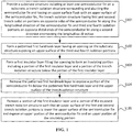
- FIG. 1 is a flowchart of a method for manufacturing a semiconductor device according to an embodiment of the present invention.
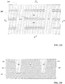
- FIGS. 2A-2C , FIGS. 3A-3C , FIGS. 4A-4C , FIGS. 5A-5C , FIGS. 6A-6D , FIGS. 7A-7C , FIGS. 8A-8C , FIGS. 9A-9C , FIGS. 10A-10B , FIGS. 11A AND 11B, and FIGS. 12A and 12B are simplified respective plan and cross-sectional views illustrating intermediate stages of a semiconductor structure in different process steps of a method of manufacturing according to some embodiments of the present invention.
- the method may include providing a semiconductor structure in step S101.
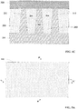
- FIG. 2A is a simplified plan view illustrating a structure of a stage in a manufacturing method of a semiconductor device in step S 101 according to an embodiment of the present invention.
- FIG. 2B is a simplified cross-sectional view illustrating a structure taken along the line A-A' of FIG. 2A .
- FIG. 2C is a simplified cross-sectional view illustrating a structure taken along the line B-B' of FIG. 2A .
- the substrate structure may include a substrate (e.g., silicon substrate) 201, one or more semiconductor fins 202 on substrate 201, and a trench isolation structure 210 surrounding the one or more semiconductor fins 201.
- trench isolation structure 210 abuts the corresponding one or more semiconductor fins 202 and has an upper surface flush with the upper surface of the one or more semiconductor fins 202.
- the one or more semiconductor fins will be referred to as the "semiconductor fin”.
- a FinFET can have one or more fins.
- exemplary embodiments will use a semiconductor fin to describe the present invention.
- the exemplary embodiments may also applied to a plurality of semiconductor fins.
- trench isolation structure 210 may include a first trench isolation portion 211 and a second trench isolation portion 212 on opposite sides of a semiconductor fin along a first direction parallel to a longitudinal direction of the semiconductor fin, and a third first trench isolation portion 213 and a fourth first trench isolation portion 214 on opposite distal ends of the semiconductor fin along a second direction intersecting the first direction, i.e., the second direction is the transverse direction to the first direction or the longitudinal direction.
- two longitudinally aligned semiconductor fins may share a same third trench isolation portion or a fourth trench isolation portion.
- the second direction is perpendicular to the longitudinal direction of the semiconductor fin.
- trench isolation structure 210 may include a trench 203 adjacent to a semiconductor fin and a dielectric layer 204 that fills the trench.
- the dielectric layer may include silicon dioxide.
- the step for forming the substrate structure may include forming an interface insulator layer (e.g., silicon dioxide) on a substrate (e.g., a silicon substrate), and forming a fourth hardmask layer (e.g., silicon nitride) on the interface insulator layer.
- the step for forming the substrate structure may further include etching the fourth hardmask layer, the interface insulator layer, and the substrate to form a semiconductor fin, wherein a trench is formed surrounding the semiconductor fin.
- the step for forming the substrate structure may further include forming a dielectric layer filling the trench using a deposition process.
- the step for forming the substrate structure may further include planarizing the dielectric layer.
- the step for forming the substrate structure may further include etching the dielectric layer in the trench to formed a recess in the dielectric layer. In one embodiment, the step for forming the substrate structure may further include removing the fourth hardmask layer. In one embodiment, the step for forming the substrate structure may further include removing the interface insulator layer and a portion of the dielectric layer to expose the semiconductor fin and such that the upper surface of the dielectric layer is flush with the upper surface of the semiconductor fin.
- the method may include forming a patterned first hardmask layer having an opening exposing an upper surface of the third and fourth trench isolation portions for the semiconductor fin on the substrate structure.
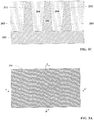
- FIG. 4A is a simplified plan view illustrating a structure of a stage in a manufacturing method of a semiconductor device in step S102 according to an embodiment of the present invention.
- FIG. 4B is a simplified cross-sectional view illustrating a structure taken along the line E-E' of FIG. 4A .
- FIG. 4C is a simplified cross-sectional view illustrating a structure taken along the line F-F' of FIG. 4A .
- a patterned first hardmask layer 320 is formed. Patterned first hardmask layer 320 has an opening 430 exposing the upper surface of respective third trench isolation portion 213 and fourth trench isolation portion 214. In one embodiment, as shown in FIGS.
- opening 430 may also expose the distal ends of the semiconductor fin in the longitudinal direction.
- the first hardmask layer may include a material having a relatively low etch selectivity relative to silicon and silicon dioxide.
- the etching process may include a reactive ion etching (RIE) and/or wet etching process.
- the first hardmask layer may include silicon nitride.
- the step of forming the first hardmask layer may include forming a hardmask layer 320 using a deposition process, as shown in FIGS. 3A , 3B, and 3C .
- the step of forming the first hardmask layer may also include forming a patterned mask layer (e.g., a photoresist not shown in the figures) on first hardmask layer 320 using a photolithography process.
- the step of forming the first hardmask layer may also include etching first hardmask layer 320 using the patterned mask layer as a mask (e.g., using RIE and/or wet etching process) to form an opening 430 exposing the upper surface of respective third trench isolation portion 213 and fourth trench isolation portion 214. .
- the step of forming the first hardmask layer may also include removing the mask layer to form a structure as shown in FIGS. 4A, 4B , and 4C .
- the method may also include forming a first insulator layer filling the opening to form an insulating portion including a portion of the first insulator layer and the underlying trench isolation structure.
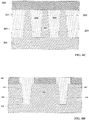
- FIG. 6A is a simplified plan view illustrating a structure of a stage in a manufacturing method of a semiconductor device in step S103 according to an embodiment of the present invention.
- FIG. 6B is a simplified cross-sectional view illustrating a structure taken along the line I-I' of FIG. 6A .
- FIG. 6C is a simplified cross-sectional view illustrating a structure taken along the line J-J' of FIG. 6A .
- a first insulator layer 540 is formed filling the opening to form an insulating portion including a portion of first insulator layer 540 and the underlying trench isolation structure.
- a first insulating portion 651 includes a first portion of first insulator layer 540 and third isolation portion 213 below the first portion of first insulator layer 540; a second insulating portion 651 includes a second portion of first insulator layer 540 and fourth isolation portion 214 below the second portion of first insulator layer 540.
- the insulating portion may include first insulating portion 651 and second insulating portion 652.
- first insulator layer 540 and third trench isolation portion 213 disposed therebelow are shown as an integrated insulating portion 651
- the second portion of first insulator layer 540 and fourth trench isolation portion 213 disposed therebelow are shown as an integrated insulating portion 652, as shown in FIG. 6D .
- First insulating portion 651 and second insulating portion 652 will be used in the drawings of subsequent steps.
- first insulator layer 540 has the same material, or different materials as that of dielectric layer 204.
- first insulator layer 540 may include silicon dioxide.
- step S103 may include forming a first insulator layer 540 on first hardmask layer 320 of the substrate structure using a deposition process, as shown in FIGS. 5A , 5B, and 5C .
- First insulator layer 540 fills opening 430 and covers first hardmask layer 320.
- step S103 may also include planarizing (e.g., chemical mechanical planarization) first insulator layer 540 to expose the upper surface of hardmask layer 320.
- the method may include performing an etch process on the third and fourth isolating portions and the distal ends of the semiconductor fin.
- the etched portion of the distal ends may range between 1 nm and 10 nm.
- the method may also include removing the first hardmask layer to expose a portion of the semiconductor fin disposed therebelow and an upper surface of the trench isolation structure.
- FIG. 7A is a simplified plan view illustrating a structure of a stage in a manufacturing method of a semiconductor device in step S104 according to an embodiment of the present invention.
- FIG. 7B is a simplified cross-sectional view illustrating a structure taken along the line K-K' of FIG. 7A .
- FIG. 7C is a simplified cross-sectional view illustrating a structure taken along the line L-L' of FIG. 7A .
- first hardmask layer 320 is removed to expose a portion of semiconductor fins 202 disposed therebelow and the upper surface of trench isolation structure 210, such as first trench isolation portion 211 and second trench isolation portion 212.
- hot phosphoric acid may be used to remove the first hardmask layer.
- the method may also include removing at least a portion of the insulator layer and a portion of the exposed trench isolation structure such that the upper surface of the first and second trench isolation portions are lower than the upper surface of the semiconductor fin to expose an upper portion of the semiconductor fin in order to expose an upper portion of the semiconductor fin and an upper portion of the isolating portion.
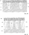
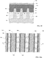
- FIG. 8A is a simplified plan view illustrating a structure of a stage in a manufacturing method of a semiconductor device in step S105 according to an embodiment of the present invention.
- FIG. 8B is a simplified cross-sectional view illustrating a structure taken along the line M-M' of FIG. 8A .
- FIG. 8C is a simplified cross-sectional view illustrating a structure taken along the line N-N' of FIG. 8A .
- At least a portion of the insulating portion e.g., first insulating portion 651 and second insulating portion 652 and at least a portion of the exposed portion of trench isolation structure 210 (e.g., first trench isolation portion 211 and second trench isolation portion 212) is removed (e.g., using RIE and/or wet etching process), such that the upper surfaces of first trench isolation portion 211 and second trench isolation portion 212 are lower than the upper surface of semiconductor fin 202 so as to expose an upper portion 801 of semiconductor fin 202 and expose an upper portion 802 of the insulating portion.
- the upper surface of the insulating portion after step S105 is substantially flush with the upper surface of the semiconductor fin, as shown in FIG. 8B .
- embodiments of the present invention provide a method of manufacturing a semiconductor device.
- the insulting portions e.g., first insulating portion 651 and second insulating portion 652 in the recess at the distal ends (in the longitudinal direction) of the semiconductor fin are raised with respect to the conventional shallow trench isolation.
- the upper surface of the insulting portions may be the same as the upper surface of the semiconductor fin, that may reduce the possibility of damage caused to the semiconductor fin in subsequent steps of removing the dummy gate (e.g., a second gate that will be described in detail below), thereby improving the device yield.
- the opening of the first hardmask layer may expose a distal end portion of the semiconductor fin in the longitudinal direction so that the formed first insulator layer may cover the distal end portion.
- the method may further include forming a first gate structure 910 that surrounds a portion of upper portion 801 of semiconductor fin 202 and a second gate structure 820 that is on upper portion 802 of the insulating portion, as shown in FIGS. 9A, 9B , and 9C .
- first gate structure 910 may include a first gate insulator layer 911 surrounding a portion of upper portion 801 of semiconductor fin, a first gate 912 on first gate insulator layer 911, and a second hardmask layer 913 on first gate 912, as shown in FIG. 9B .
- first gate insulator layer 911 may include silicon dioxide
- first gate 912 may include polysilicon
- second hardmask layer 913 may include silicon nitride.
- second gate structure 920 may include a second gate insulator layer 921 on upper portion 802 of the insulating portion, a second gate 922 on second gate insulator layer 921, and a third hardmask layer 923 on second gate 922, as shown in FIG. 9B .
- second gate insulator layer 921 may include silicon dioxide
- second gate 922 may include polysilicon
- third hardmask layer 923 may include silicon nitride.
- the first and second gate insulator layer are formed using a same process. The first and second gates are formed concurrently in a same gate forming process.
- the second and third hardmask layers are formed in a same hardmask forming process.
- the method may further include spacers 930 on opposite sides of first gate structure 910 and on opposite sides of second gate structure 920, as shown in FIGS. 10A and 10B .
- Spacers 930 cover the distal ends of the semiconductor fin in the longitudinal direction.
- spacers 930 may include silicon nitride.
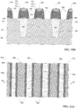
- the method may further include performing an etching process on portions of the semiconductor fin that are not covered by first gate structure 910 and spacers 930 to form a recess, as shown in FIGS. 11A and 11B .
- the etching process may include a self-aligning etching process.
- the recess may include a first recess 941 and a second recess 942 disposed on opposite sides of first gate structure 910.
- the method may further include forming a source or drain having a different material than that of the semiconductor fin.
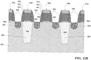
- a source 951 is formed in first recess 941
- a drain 952 is formed in second recess 942 using, e.g., an epitaxial process, as shown in FIGS. 12A and 12B .
- the semiconductor device thus manufactured has a source or drain with more regular morphology and improved performance.
- the lateral dimension between the second gate and the distal ends of the semiconductor fin may be adjusted, for example, the distance between the second gate and the distal ends of the semiconductor fin can be relatively large, e.g., the lateral distance between second gate and the distal ends of the semiconductor fin may be in the range of 2 nm and 20 nm, so that the likelihood of causing damage to the semiconductor fin can be reduced in subsequent step of removing the second gate.
- the method of manufacturing a semiconductor device can provide process flexibility and wide process windows so that damage to the semiconductor fin can be reduced during the removal of a dummy gate (e.g., a second gate).
- a dummy gate e.g., a second gate
- Embodiments of the present invention also provide a semiconductor device.
- the semiconductor device may include a substrate 201, at least one semiconductor fin 202 on substrate 201, and a trench isolation structure 210 surrounding the semiconductor fin.
- trench isolation structure 210 is adjacent to semiconductor fin 202.
- trench isolation structure 210 may include a first trench isolation portion 211 and a second trench isolation portion 212 on opposite sides of the semiconductor fin along a first direction parallel to the longitudinal direction of the semiconductor fin, as shown in FIGS. 8A , 8B, and 8C .
- first trench isolation portion 211 and second trench isolation portion 212 each have an upper surface that is lower than the upper surface of semiconductor fins 202, thereby exposing an upper portion 801 of semiconductor fin 202 and an upper potion 802 of a first insulating portion 651 and a second insulating portion 652.
- the trench isolation structure may include a trench 203 adjacent to the semiconductor fin and a dielectric layer 204 filling trench 203.
- Dielectric layer 204 may include silicon dioxide.
- Embodiments of the present invention also provide a semiconductor device, as shown in FIGS. 12A and 12B .
- the semiconductor device of FIGS. 12A and 12B may include the same or structure as that of the semiconductor device of FIGS. 8A , 8B, and 8C , that has been described in detail in above sections, and will not be repeated herein for the sake of brevity.
- the semiconductor device may further include a first gate structure 910 surrounding a portion of first upper portion 801 of semiconductor fins 202 and a second gate structure 920 disposed on a second upper portion 802 of a second gate structure 920.
- first gate structure 910 may include a first gate insulator layer 911 surrounding a portion of first upper portion 801, a first gate 912 on first gate insulator layer 911, and a second hardmask layer 913 on first gate 912.
- the first gate insulator layer may include silicon dioxide
- the first gate may include polysilicon
- the second hardmask layer may include silicon nitride.
- second gate structure 920 may include a second gate insulator layer 921 on second upper portion 802, a second gate 922 on second gate insulator layer 921, and a third hardmask layer 923 on second gate 922.
- the second gate insulator layer may include silicon dioxide
- the second gate may include polysilicon
- the third hardmask layer may include silicon nitride.
- the semiconductor device may further include spacers 930 on opposite side surfaces of first gate structure 910 and on the surface on opposite sides of second gate structure 920. Spacers 930 opposite side surfaces of second gate structure 920 cover the distal ends of the semiconductor fin in the longitudinal direction.
- spacers 930 may include silicon nitride.
- the semiconductor device may further include a source 951 and a drain 952 formed on opposite sides of first gate structure 910 and have a material different from the material of the semiconductor fin.
- the semiconductor device may include a source and a drain that have a more regular morphology, so that the performance and yield of the device can be improved, and the likelihood of damage caused to the semiconductor device during the removal of the dummy gate (e.g., the above-described second gate) is reduced.
- the dummy gate e.g., the above-described second gate
- references in the specification to "one embodiment”, “an embodiment”, “an example embodiment”, “some embodiments”, etc., indicate that the embodiment described may include a particular feature, structure, or characteristic, but every embodiment may not necessarily include the particular feature, structure, or characteristic. Moreover, such phrases are not necessarily referring to the same embodiment. Further, when a particular feature, structure, or characteristic is described in connection with an embodiment, it is submitted that it is within the knowledge of one skilled in the art to affect such feature, structure, or characteristic in connection with other embodiments whether or not explicitly described.
- embodiments of the present invention provide a detailed description of a method of manufacturing a semiconductor device and a semiconductor device manufactured by the described method. Details of well-known processes are omitted in order not to obscure the concepts presented herein.
Landscapes
- Insulated Gate Type Field-Effect Transistor (AREA)
Applications Claiming Priority (1)
| Application Number | Priority Date | Filing Date | Title |
|---|---|---|---|
| CN201610510635.5A CN107564859B (zh) | 2016-07-01 | 2016-07-01 | 半导体装置及其制造方法 |
Publications (1)
| Publication Number | Publication Date |
|---|---|
| EP3264471A1 true EP3264471A1 (de) | 2018-01-03 |
Family
ID=59276516
Family Applications (1)
| Application Number | Title | Priority Date | Filing Date |
|---|---|---|---|
| EP17178152.9A Withdrawn EP3264471A1 (de) | 2016-07-01 | 2017-06-27 | Verbesserte epi-integralität auf source-/drain-bereichen von finfet |
Country Status (3)
| Country | Link |
|---|---|
| US (1) | US10332980B2 (de) |
| EP (1) | EP3264471A1 (de) |
| CN (1) | CN107564859B (de) |
Families Citing this family (6)
| Publication number | Priority date | Publication date | Assignee | Title |
|---|---|---|---|---|
| KR102458311B1 (ko) | 2018-04-11 | 2022-10-24 | 삼성전자주식회사 | 집적회로 소자 |
| KR102479996B1 (ko) | 2018-05-17 | 2022-12-20 | 삼성전자주식회사 | 반도체 장치 |
| US10475693B1 (en) | 2018-06-07 | 2019-11-12 | Globalfoundries Inc. | Method for forming single diffusion breaks between finFET devices and the resulting devices |
| DE102018126937B4 (de) | 2018-07-31 | 2021-01-28 | Taiwan Semiconductor Manufacturing Co., Ltd. | Finnenschnitt-Isolationsbereiche und Verfahren zu ihrem Bilden |
| US11171236B2 (en) * | 2018-07-31 | 2021-11-09 | Taiwan Semiconductor Manufacturing Company, Ltd. | Cut-fin isolation regions and method forming same |
| US11854863B2 (en) * | 2021-06-24 | 2023-12-26 | Taiwan Semiconductor Manufacturing Company Ltd. | Semiconductor device including an isolation region having an edge being covered and manufacturing method for the same |
Citations (3)
| Publication number | Priority date | Publication date | Assignee | Title |
|---|---|---|---|---|
| US20140117454A1 (en) * | 2012-10-26 | 2014-05-01 | Taiwan Semiconductor Manufacturing Company, Ltd. | FinFET with Dummy Gate on Non-Recessed Shallow Trench Isolation (STI) |
| US20150187571A1 (en) * | 2013-12-27 | 2015-07-02 | Taiwan Semiconductor Manufacturing Company, Ltd. | Germanium-Containing FinFET and Methods for Forming the Same |
| US20160104673A1 (en) * | 2014-10-09 | 2016-04-14 | United Microelectronics Corp. | Fin-shaped field-effect transistor with a germanium epitaxial cap and a method for fabricating the same |
Family Cites Families (3)
| Publication number | Priority date | Publication date | Assignee | Title |
|---|---|---|---|---|
| US9559181B2 (en) * | 2013-11-26 | 2017-01-31 | Taiwan Semiconductor Manufacturing Company, Ltd. | Structure and method for FinFET device with buried sige oxide |
| US9368496B1 (en) * | 2015-01-30 | 2016-06-14 | Globalfoundries Inc. | Method for uniform recess depth and fill in single diffusion break for fin-type process and resulting devices |
| CN107045979B (zh) * | 2016-02-05 | 2019-11-01 | 中芯国际集成电路制造(上海)有限公司 | 半导体结构的形成方法 |
-
2016
- 2016-07-01 CN CN201610510635.5A patent/CN107564859B/zh active Active
-
2017
- 2017-06-02 US US15/612,805 patent/US10332980B2/en active Active
- 2017-06-27 EP EP17178152.9A patent/EP3264471A1/de not_active Withdrawn
Patent Citations (3)
| Publication number | Priority date | Publication date | Assignee | Title |
|---|---|---|---|---|
| US20140117454A1 (en) * | 2012-10-26 | 2014-05-01 | Taiwan Semiconductor Manufacturing Company, Ltd. | FinFET with Dummy Gate on Non-Recessed Shallow Trench Isolation (STI) |
| US20150187571A1 (en) * | 2013-12-27 | 2015-07-02 | Taiwan Semiconductor Manufacturing Company, Ltd. | Germanium-Containing FinFET and Methods for Forming the Same |
| US20160104673A1 (en) * | 2014-10-09 | 2016-04-14 | United Microelectronics Corp. | Fin-shaped field-effect transistor with a germanium epitaxial cap and a method for fabricating the same |
Also Published As
| Publication number | Publication date |
|---|---|
| CN107564859A (zh) | 2018-01-09 |
| US20180006135A1 (en) | 2018-01-04 |
| US10332980B2 (en) | 2019-06-25 |
| CN107564859B (zh) | 2020-02-28 |
Similar Documents
| Publication | Publication Date | Title |
|---|---|---|
| US10332980B2 (en) | EPI integrality on source/drain region of FinFET | |
| US10170375B2 (en) | FinFET devices with unique fin shape and the fabrication thereof | |
| CN108122768B (zh) | 半导体装置的形成方法 | |
| CN101577278B (zh) | 半导体结构及其形成方法 | |
| US7381618B2 (en) | Gate etch process for a high-voltage FET | |
| KR101368021B1 (ko) | 메모리 셀 어레이 형성 방법, 복수의 전계 효과 트랜지스터 형성 방법, 소스/드레인 영역 및 분리 트렌치 형성 방법, 및 기판 내로 일련의 이격 트렌치 형성 방법 | |
| US9935179B2 (en) | Method for making semiconductor device with filled gate line end recesses | |
| US9601568B2 (en) | Semiconductor device including STI structure | |
| CN102113110A (zh) | 具有扩展的有源区的半导体器件 | |
| CN107342322A (zh) | 半导体装置的鳍状结构以及鳍式场效晶体管装置 | |
| CN110634744B (zh) | 具有应力有源区的半导体器件及其形成方法 | |
| US10325813B2 (en) | Fin cut process and fin structure | |
| US20160380081A1 (en) | Finfet and method of fabricating the same | |
| US10347629B2 (en) | FinFET device | |
| TWI728966B (zh) | 半導體元件及其製作方法 | |
| CN115241272A (zh) | 半导体元件 | |
| KR100549579B1 (ko) | 셀 트랜지스터의 제조 방법 | |
| KR101051809B1 (ko) | 고전압 소자 및 그의 제조방법 | |
| KR100675887B1 (ko) | 반도체 소자의 트렌치 소자분리막 및 그 형성 방법 | |
| CN120435052A (zh) | 半导体结构的形成方法 | |
| KR101194742B1 (ko) | 반도체 소자의 형성 방법 | |
| CN120857537A (zh) | 半导体结构的形成方法 | |
| KR20070032475A (ko) | 반도체 소자의 제조방법 | |
| KR20040082751A (ko) | 플래시 메모리 소자의 제조 방법 |
Legal Events
| Date | Code | Title | Description |
|---|---|---|---|
| PUAI | Public reference made under article 153(3) epc to a published international application that has entered the european phase |
Free format text: ORIGINAL CODE: 0009012 |
|
| STAA | Information on the status of an ep patent application or granted ep patent |
Free format text: STATUS: THE APPLICATION HAS BEEN PUBLISHED |
|
| AK | Designated contracting states |
Kind code of ref document: A1 Designated state(s): AL AT BE BG CH CY CZ DE DK EE ES FI FR GB GR HR HU IE IS IT LI LT LU LV MC MK MT NL NO PL PT RO RS SE SI SK SM TR |
|
| AX | Request for extension of the european patent |
Extension state: BA ME |
|
| STAA | Information on the status of an ep patent application or granted ep patent |
Free format text: STATUS: REQUEST FOR EXAMINATION WAS MADE |
|
| 17P | Request for examination filed |
Effective date: 20180430 |
|
| RBV | Designated contracting states (corrected) |
Designated state(s): AL AT BE BG CH CY CZ DE DK EE ES FI FR GB GR HR HU IE IS IT LI LT LU LV MC MK MT NL NO PL PT RO RS SE SI SK SM TR |
|
| RAP1 | Party data changed (applicant data changed or rights of an application transferred) |
Owner name: SEMICONDUCTOR MANUFACTURING INTERNATIONAL (BEIJING Owner name: SEMICONDUCTOR MANUFACTURING INTERNATIONAL (SHANGHA |
|
| STAA | Information on the status of an ep patent application or granted ep patent |
Free format text: STATUS: EXAMINATION IS IN PROGRESS |
|
| 17Q | First examination report despatched |
Effective date: 20200309 |
|
| STAA | Information on the status of an ep patent application or granted ep patent |
Free format text: STATUS: THE APPLICATION IS DEEMED TO BE WITHDRAWN |
|
| 18D | Application deemed to be withdrawn |
Effective date: 20200721 |