EP3258554B1 - Laserkristallisierungsverfahren und -vorrichtung - Google Patents
Laserkristallisierungsverfahren und -vorrichtung Download PDFInfo
- Publication number
- EP3258554B1 EP3258554B1 EP17175915.2A EP17175915A EP3258554B1 EP 3258554 B1 EP3258554 B1 EP 3258554B1 EP 17175915 A EP17175915 A EP 17175915A EP 3258554 B1 EP3258554 B1 EP 3258554B1
- Authority
- EP
- European Patent Office
- Prior art keywords
- mirror
- laser beams
- cleaning
- transparent window
- laser
- Prior art date
- Legal status (The legal status is an assumption and is not a legal conclusion. Google has not performed a legal analysis and makes no representation as to the accuracy of the status listed.)
- Active
Links
Images








Classifications
-
- H—ELECTRICITY
- H10—SEMICONDUCTOR DEVICES; ELECTRIC SOLID-STATE DEVICES NOT OTHERWISE PROVIDED FOR
- H10P—GENERIC PROCESSES OR APPARATUS FOR THE MANUFACTURE OR TREATMENT OF DEVICES COVERED BY CLASS H10
- H10P34/00—Irradiation with electromagnetic or particle radiation of wafers, substrates or parts of devices
- H10P34/40—Irradiation with electromagnetic or particle radiation of wafers, substrates or parts of devices with high-energy radiation
- H10P34/42—Irradiation with electromagnetic or particle radiation of wafers, substrates or parts of devices with high-energy radiation with electromagnetic radiation, e.g. laser annealing
-
- H—ELECTRICITY
- H01—ELECTRIC ELEMENTS
- H01S—DEVICES USING THE PROCESS OF LIGHT AMPLIFICATION BY STIMULATED EMISSION OF RADIATION [LASER] TO AMPLIFY OR GENERATE LIGHT; DEVICES USING STIMULATED EMISSION OF ELECTROMAGNETIC RADIATION IN WAVE RANGES OTHER THAN OPTICAL
- H01S3/00—Lasers, i.e. devices using stimulated emission of electromagnetic radiation in the infrared, visible or ultraviolet wave range
- H01S3/02—Constructional details
- H01S3/03—Constructional details of gas laser discharge tubes
- H01S3/034—Optical devices within, or forming part of, the tube, e.g. windows, mirrors
- H01S3/0346—Protection of windows or mirrors against deleterious effects
-
- H—ELECTRICITY
- H10—SEMICONDUCTOR DEVICES; ELECTRIC SOLID-STATE DEVICES NOT OTHERWISE PROVIDED FOR
- H10P—GENERIC PROCESSES OR APPARATUS FOR THE MANUFACTURE OR TREATMENT OF DEVICES COVERED BY CLASS H10
- H10P14/00—Formation of materials, e.g. in the shape of layers or pillars
- H10P14/20—Formation of materials, e.g. in the shape of layers or pillars of semiconductor materials
- H10P14/38—Formation of materials, e.g. in the shape of layers or pillars of semiconductor materials characterised by treatments done after the formation of the materials
- H10P14/3802—Crystallisation or recrystallisation of non-monocrystalline semiconductor materials, e.g. regrowth
- H10P14/3808—Crystallisation or recrystallisation of non-monocrystalline semiconductor materials, e.g. regrowth using laser beams
-
- H—ELECTRICITY
- H01—ELECTRIC ELEMENTS
- H01S—DEVICES USING THE PROCESS OF LIGHT AMPLIFICATION BY STIMULATED EMISSION OF RADIATION [LASER] TO AMPLIFY OR GENERATE LIGHT; DEVICES USING STIMULATED EMISSION OF ELECTROMAGNETIC RADIATION IN WAVE RANGES OTHER THAN OPTICAL
- H01S3/00—Lasers, i.e. devices using stimulated emission of electromagnetic radiation in the infrared, visible or ultraviolet wave range
- H01S3/02—Constructional details
- H01S3/04—Arrangements for thermal management
- H01S3/0401—Arrangements for thermal management of optical elements being part of laser resonator, e.g. windows, mirrors, lenses
-
- B—PERFORMING OPERATIONS; TRANSPORTING
- B23—MACHINE TOOLS; METAL-WORKING NOT OTHERWISE PROVIDED FOR
- B23K—SOLDERING OR UNSOLDERING; WELDING; CLADDING OR PLATING BY SOLDERING OR WELDING; CUTTING BY APPLYING HEAT LOCALLY, e.g. FLAME CUTTING; WORKING BY LASER BEAM
- B23K26/00—Working by laser beam, e.g. welding, cutting or boring
- B23K26/50—Working by transmitting the laser beam through or within the workpiece
- B23K26/53—Working by transmitting the laser beam through or within the workpiece for modifying or reforming the material inside the workpiece, e.g. for producing break initiation cracks
-
- C—CHEMISTRY; METALLURGY
- C30—CRYSTAL GROWTH
- C30B—SINGLE-CRYSTAL GROWTH; UNIDIRECTIONAL SOLIDIFICATION OF EUTECTIC MATERIAL OR UNIDIRECTIONAL DEMIXING OF EUTECTOID MATERIAL; REFINING BY ZONE-MELTING OF MATERIAL; PRODUCTION OF A HOMOGENEOUS POLYCRYSTALLINE MATERIAL WITH DEFINED STRUCTURE; SINGLE CRYSTALS OR HOMOGENEOUS POLYCRYSTALLINE MATERIAL WITH DEFINED STRUCTURE; AFTER-TREATMENT OF SINGLE CRYSTALS OR A HOMOGENEOUS POLYCRYSTALLINE MATERIAL WITH DEFINED STRUCTURE; APPARATUS THEREFOR
- C30B1/00—Single-crystal growth directly from the solid state
- C30B1/02—Single-crystal growth directly from the solid state by thermal treatment, e.g. strain annealing
- C30B1/026—Solid phase epitaxial growth through a disordered intermediate layer
-
- G—PHYSICS
- G02—OPTICS
- G02B—OPTICAL ELEMENTS, SYSTEMS OR APPARATUS
- G02B1/00—Optical elements characterised by the material of which they are made; Optical coatings for optical elements
- G02B1/10—Optical coatings produced by application to, or surface treatment of, optical elements
- G02B1/18—Coatings for keeping optical surfaces clean, e.g. hydrophobic or photo-catalytic films
-
- H—ELECTRICITY
- H01—ELECTRIC ELEMENTS
- H01S—DEVICES USING THE PROCESS OF LIGHT AMPLIFICATION BY STIMULATED EMISSION OF RADIATION [LASER] TO AMPLIFY OR GENERATE LIGHT; DEVICES USING STIMULATED EMISSION OF ELECTROMAGNETIC RADIATION IN WAVE RANGES OTHER THAN OPTICAL
- H01S3/00—Lasers, i.e. devices using stimulated emission of electromagnetic radiation in the infrared, visible or ultraviolet wave range
- H01S3/005—Optical devices external to the laser cavity, specially adapted for lasers, e.g. for homogenisation of the beam or for manipulating laser pulses, e.g. pulse shaping
-
- H—ELECTRICITY
- H01—ELECTRIC ELEMENTS
- H01S—DEVICES USING THE PROCESS OF LIGHT AMPLIFICATION BY STIMULATED EMISSION OF RADIATION [LASER] TO AMPLIFY OR GENERATE LIGHT; DEVICES USING STIMULATED EMISSION OF ELECTROMAGNETIC RADIATION IN WAVE RANGES OTHER THAN OPTICAL
- H01S3/00—Lasers, i.e. devices using stimulated emission of electromagnetic radiation in the infrared, visible or ultraviolet wave range
- H01S3/02—Constructional details
- H01S3/03—Constructional details of gas laser discharge tubes
-
- H—ELECTRICITY
- H01—ELECTRIC ELEMENTS
- H01S—DEVICES USING THE PROCESS OF LIGHT AMPLIFICATION BY STIMULATED EMISSION OF RADIATION [LASER] TO AMPLIFY OR GENERATE LIGHT; DEVICES USING STIMULATED EMISSION OF ELECTROMAGNETIC RADIATION IN WAVE RANGES OTHER THAN OPTICAL
- H01S3/00—Lasers, i.e. devices using stimulated emission of electromagnetic radiation in the infrared, visible or ultraviolet wave range
- H01S3/02—Constructional details
- H01S3/03—Constructional details of gas laser discharge tubes
- H01S3/038—Electrodes, e.g. special shape, configuration or composition
-
- H—ELECTRICITY
- H01—ELECTRIC ELEMENTS
- H01S—DEVICES USING THE PROCESS OF LIGHT AMPLIFICATION BY STIMULATED EMISSION OF RADIATION [LASER] TO AMPLIFY OR GENERATE LIGHT; DEVICES USING STIMULATED EMISSION OF ELECTROMAGNETIC RADIATION IN WAVE RANGES OTHER THAN OPTICAL
- H01S3/00—Lasers, i.e. devices using stimulated emission of electromagnetic radiation in the infrared, visible or ultraviolet wave range
- H01S3/09—Processes or apparatus for excitation, e.g. pumping
- H01S3/097—Processes or apparatus for excitation, e.g. pumping by gas discharge of a gas laser
- H01S3/0971—Processes or apparatus for excitation, e.g. pumping by gas discharge of a gas laser transversely excited
-
- H—ELECTRICITY
- H01—ELECTRIC ELEMENTS
- H01S—DEVICES USING THE PROCESS OF LIGHT AMPLIFICATION BY STIMULATED EMISSION OF RADIATION [LASER] TO AMPLIFY OR GENERATE LIGHT; DEVICES USING STIMULATED EMISSION OF ELECTROMAGNETIC RADIATION IN WAVE RANGES OTHER THAN OPTICAL
- H01S3/00—Lasers, i.e. devices using stimulated emission of electromagnetic radiation in the infrared, visible or ultraviolet wave range
- H01S3/14—Lasers, i.e. devices using stimulated emission of electromagnetic radiation in the infrared, visible or ultraviolet wave range characterised by the material used as the active medium
- H01S3/22—Gases
- H01S3/223—Gases the active gas being polyatomic, i.e. containing two or more atoms
- H01S3/225—Gases the active gas being polyatomic, i.e. containing two or more atoms comprising an excimer or exciplex
-
- H—ELECTRICITY
- H01—ELECTRIC ELEMENTS
- H01S—DEVICES USING THE PROCESS OF LIGHT AMPLIFICATION BY STIMULATED EMISSION OF RADIATION [LASER] TO AMPLIFY OR GENERATE LIGHT; DEVICES USING STIMULATED EMISSION OF ELECTROMAGNETIC RADIATION IN WAVE RANGES OTHER THAN OPTICAL
- H01S5/00—Semiconductor lasers
- H01S5/02—Structural details or components not essential to laser action
- H01S5/0206—Substrates, e.g. growth, shape, material, removal or bonding
-
- H—ELECTRICITY
- H10—SEMICONDUCTOR DEVICES; ELECTRIC SOLID-STATE DEVICES NOT OTHERWISE PROVIDED FOR
- H10D—INORGANIC ELECTRIC SEMICONDUCTOR DEVICES
- H10D86/00—Integrated devices formed in or on insulating or conducting substrates, e.g. formed in silicon-on-insulator [SOI] substrates or on stainless steel or glass substrates
- H10D86/01—Manufacture or treatment
- H10D86/021—Manufacture or treatment of multiple TFTs
- H10D86/0221—Manufacture or treatment of multiple TFTs comprising manufacture, treatment or patterning of TFT semiconductor bodies
- H10D86/0223—Manufacture or treatment of multiple TFTs comprising manufacture, treatment or patterning of TFT semiconductor bodies comprising crystallisation of amorphous, microcrystalline or polycrystalline semiconductor materials
-
- H—ELECTRICITY
- H10—SEMICONDUCTOR DEVICES; ELECTRIC SOLID-STATE DEVICES NOT OTHERWISE PROVIDED FOR
- H10P—GENERIC PROCESSES OR APPARATUS FOR THE MANUFACTURE OR TREATMENT OF DEVICES COVERED BY CLASS H10
- H10P72/00—Handling or holding of wafers, substrates or devices during manufacture or treatment thereof
- H10P72/04—Apparatus for manufacture or treatment
- H10P72/0431—Apparatus for thermal treatment
- H10P72/0436—Apparatus for thermal treatment mainly by radiation
-
- B—PERFORMING OPERATIONS; TRANSPORTING
- B23—MACHINE TOOLS; METAL-WORKING NOT OTHERWISE PROVIDED FOR
- B23K—SOLDERING OR UNSOLDERING; WELDING; CLADDING OR PLATING BY SOLDERING OR WELDING; CUTTING BY APPLYING HEAT LOCALLY, e.g. FLAME CUTTING; WORKING BY LASER BEAM
- B23K2103/00—Materials to be soldered, welded or cut
- B23K2103/50—Inorganic materials other than metals or composite materials
- B23K2103/56—Inorganic materials other than metals or composite materials being semiconducting
-
- H—ELECTRICITY
- H01—ELECTRIC ELEMENTS
- H01S—DEVICES USING THE PROCESS OF LIGHT AMPLIFICATION BY STIMULATED EMISSION OF RADIATION [LASER] TO AMPLIFY OR GENERATE LIGHT; DEVICES USING STIMULATED EMISSION OF ELECTROMAGNETIC RADIATION IN WAVE RANGES OTHER THAN OPTICAL
- H01S3/00—Lasers, i.e. devices using stimulated emission of electromagnetic radiation in the infrared, visible or ultraviolet wave range
- H01S3/02—Constructional details
- H01S3/04—Arrangements for thermal management
- H01S3/0407—Liquid cooling, e.g. by water
-
- H—ELECTRICITY
- H01—ELECTRIC ELEMENTS
- H01S—DEVICES USING THE PROCESS OF LIGHT AMPLIFICATION BY STIMULATED EMISSION OF RADIATION [LASER] TO AMPLIFY OR GENERATE LIGHT; DEVICES USING STIMULATED EMISSION OF ELECTROMAGNETIC RADIATION IN WAVE RANGES OTHER THAN OPTICAL
- H01S3/00—Lasers, i.e. devices using stimulated emission of electromagnetic radiation in the infrared, visible or ultraviolet wave range
- H01S3/02—Constructional details
- H01S3/04—Arrangements for thermal management
- H01S3/041—Arrangements for thermal management for gas lasers
Definitions
- Embodiments of the present disclosure are generally directed to a laser crystallization method and device. More particularly, embodiments of the present disclosure are generally directed to a laser crystallization method and device that crystallizes amorphous silicon into polycrystalline silicon.
- Pixels of active matrix type display devices such as an organic light emitting devices (OLED) or a liquid crystal displays (LCD) comprise thin film transistors (TFTs) that include semiconductor layers.
- a semiconductor layer is typically made of polycrystalline silicon. Polycrystalline silicon has high mobility and is appropriate for organic light emitting devices to control brightness of emission layers based on current.
- Polycrystalline silicon can be generated by irradiating laser beams onto amorphous silicon and performing an annealing process thereto, during which a laser crystallization device is used.
- the laser crystallization device may be a gas laser device, such as an excimer laser device.
- a laser crystallization device excites a gas medium by an electric discharge process to generate laser beams, amplifies the laser beams by resonance, and outputs the resultant laser beams.
- Embodiments of the present disclosure can provide a laser crystallization method and device that reduces component contamination and increases a replacement period.
- An exemplary embodiment provides a laser crystallization method that includes exciting a gas medium in an airtight container to generate laser beams; amplifying the laser beams by reflecting the laser beams between a high reflection mirror and a low reflection mirror respectively disposed facing opposite end portions of the airtight container, wherein a first transparent window and a second transparent window fixed to respective end portions of the airtight container, and outputting the amplified laser beams; and disposing a cleaning mirror in a path of the laser beams that have propagated through the second transparent window.
- the cleaning mirror reflects the laser beams that have propagated through the second transparent window, especially all of the laser beams that have propagated through the second transparent window, back through the second transparent window. As by this reflection of laser beams back from the outside to the inside of the airtight container, contaminations on the second transparent window are removed, the mirror is named as cleaning mirror.
- Outputting the amplified laser beams may define a running state for in which the laser beams are irradiated to an irradiation target, and disposing the cleaning mirror may define an idle state of waiting for a next execution.
- the cleaning mirror may be moved away from the path of laser beams during the outputting of amplified laser beams.
- the cleaning mirror is combined with a transfer device that displaces the cleaning mirror between a first position in the path of the laser beams and a second position away from and out of the path of the laser beams.
- the transfer device may include a driving motor and a mirror frame that is rotated by the driving motor and that fixes the cleaning mirror.
- the cleaning mirror may be displaced between the first position and the second position by rotation of the mirror frame.
- the transfer device may include a driving motor, and a mirror frame that is linearly displaced by the driving motor and that fixes the cleaning mirror.
- the cleaning mirror may be displaced between the first position and the second position by linear motion of the mirror frame.
- the low reflection mirror and the cleaning mirror may be combined with the transfer device which exchanges positions thereof between outputting the amplified laser beams and disposing the cleaning mirror.
- the transfer device may include a driving motor and a mirror frame that is rotated by the driving motor and that fixes the low reflection mirror and the cleaning mirror. The positions of the low reflection mirror and the cleaning mirror may be exchanged by rotating the mirror frame.
- the low reflection mirror and the cleaning mirror may be combined with the transfer device, and the low reflection mirror may be moved away from the path of the laser beams when disposing the cleaning mirror.
- the transfer device may include a driving motor and a mirror frame that is linearly displaced by the driving motor and that fixes the low reflection mirror and the cleaning mirror.
- One of the low reflection mirror and the cleaning mirror may be disposed to face the second transparent window by a linear displacement of the mirror frame.
- a laser crystallization device that includes an airtight container that is a gas laser device charged with a gas medium, a first transparent window and a second transparent window fixed to respective end portions of the airtight container that face each other along the center axis of the airtight container, a high reflection mirror installed outside the first transparent window and a low reflection mirror installed outside the second transparent window, wherein the low reflection mirror has a reflectivity that is lower than its transmittance, and a cleaning mirror.
- laser beams are output from the airtight container through the second transparent window and the low reflection mirror to an irradiation target, and the cleaning mirror is positioned away from and out of a path of laser beams output from the airtight container.
- the cleaning mirror is disposed in the path of the laser beams output from the airtight container, wherein the laser beams are reflected back into the airtight container.
- the laser crystallization device may further include a shutter that transmits respectively allows transmitting laser beams propagating through the low reflection mirror in the running state, and blocks laser beams propagating through the low reflection mirror in the idle state.
- the low reflection mirror and the cleaning mirror may be combined with a transfer device, and one of the low reflection mirror and the cleaning mirror may be disposed in the path of the laser beams by operation of the transfer device.
- the transfer device may include a driving motor and a mirror frame that is rotated by the driving motor and that fixes the low reflection mirror and the cleaning mirror, and the positions of the low reflection mirror and the cleaning mirror are exchanged by rotating the mirror frame.
- the transfer device may include a driving motor and a mirror frame that is linearly translated by the driving motor and that fixes the low reflection mirror and the cleaning mirror, and one of the low reflection mirror and the cleaning mirror is disposed to face the second transparent window by linear translation of the mirror frame.
- the cleaning mirror may be combined with a transfer device that displaces the cleaning mirror between a first position in the path of the laser beams and a second position away from and out of the path of the laser beams.
- the transfer device may include a driving motor and a mirror frame that is rotated by the driving motor and that fixes the cleaning mirror, and the cleaning mirror is displaced between the first position and the second position by rotation of the mirror frame.
- the transfer device may include a driving motor and a mirror frame that is linearly displaced by the driving motor and that fixes the cleaning mirror, and the cleaning mirror is displaced between the first position and the second position by linear motion of the mirror frame.
- the laser beams reflected back into the airtight container may remove contamination material attached to an internal side of the second transparent window.
- the laser crystallization device may further include a pair of electrodes symmetrically disposed with respect to a center of the airtight container, a high-voltage power supply connected to one of the pair of electrodes, a reflection mirror that changes a propagation direction of the laser beams; and a condensing lens that condenses the laser beams to the irradiation target.
- a voltage is applied to the electrodes, the gas medium is excited to generate laser beams.
- contamination of the second transparent window can be reduced by the cleaning mirror to maintain a high transmittance for a long time frame.
- a replacement period of the second transparent window may be increased, and an operational cost of a laser crystallization device may be reduced.
- any part such as a layer, film, region, or plate, is positioned on another part, it means the part is directly on the other part or above the other part with at least one intermediate part.
- FIG. 1 and FIG. 2 are schematic diagrams of a laser crystallization device according to an exemplary embodiment.
- a laser crystallization device 100 includes an airtight container 10 charged with a gas medium, a pair of electrodes 20 installed in the airtight container 10, a laser resonance portion 30 installed outside the airtight container 10, and a cleaning mirror 40.
- the laser crystallization device 100 is a gas laser device, such as an excimer laser device, that is a high-power ultraviolet laser device.
- the word excimer indicates that molecules are stable in the excited state.
- the gas medium in the airtight container 10 is a mixture gas of a rare gas such as Kr, Ar, and Xe, and hydrogen chloride (HCI).
- the airtight container 10 has a cylindrical shape, and the pair of electrodes 20 are symmetrically disposed with respect to a center axis (shown with dashed lines) of the airtight container 10.
- One of the pair of electrodes 20 is grounded and the other thereof is connected to a high-voltage power supply 21.
- a voltage is applied to the electrode 20, a discharge occurs between the pair of electrodes 20 and the gas medium is excited to generate the laser beams.
- a first transparent window 11 and a second transparent window 12 are fixed to respective end portions of the airtight container 10.
- the first transparent window 11 and the second transparent window 12 face each other along the center axis of the airtight container 10 and transmit the laser beams.
- the first transparent window 11 and the second transparent window 12 may be made of glass or sapphire, and an anti-reflection coating layer that increases transmittance may be provided on a surface thereof.
- the laser resonance portion 30 includes a high reflection mirror 31 installed outside the first transparent window 11, especially outside the airtight container 10 and facing the first transparent window 11, and a low reflection mirror 32 installed outside the second transparent window 12, especially outside the airtight container 10 and facing the second transparent window 12.
- the high reflection mirror 31 has a reflectivity that is close to 100 %.
- the low reflection mirror 32 has a reflectivity that is lower than its transmittance. For example, it may have about 10 % reflectivity and about 90 % transmittance.
- the laser beams transmitted through the first transparent window 11 are reflected by the high reflection mirror 31.
- a portion of the laser beams transmitted through the second transparent window 12 is reflected by the low reflection mirror 32 and the remaining portion thereof is transmitted through the low reflection mirror 32.
- the laser beams propagate between the high reflection mirror 31 and the low reflection mirror 32 to generate resonance and be amplified.
- the amplified laser beams especially only the amplified laser beams but not the unamplified laser beams or laser beams with comparatively lower amplification or intensity, propagate through the low reflection mirror 32 and are output to an irradiation target.
- the laser crystallization device 100 includes a fan motor and a cooling pipe combined with the airtight container 10.
- the fan motor circulates the gas medium in the airtight container 10, and the cooling pipe cools the gas medium by heat-exchanging the gas medium with cooling water.
- the laser crystallization device 100 includes a shutter 51, a reflection mirror 52, and a condensing lens 53 installed outside the low reflection mirror 32.
- the shutter 51 transmits respectively enables transmission of or blocks the laser beams (LB) propagating through the low reflection mirror 32.
- the reflection mirror 52 changes a propagation direction of the laser beams, and the condensing lens 53 condenses the laser beams to the irradiation target.
- the irradiation target is an amorphous silicon layer 62 provided on a substrate 61.
- the amorphous silicon layer 62 is crystallized into a polycrystalline silicon layer by annealing caused by irradiation of laser beams.
- the substrate 61 and the amorphous silicon layer 62 are fixed to a stage 63, and the stage 63 can move the substrate 61 and the amorphous silicon layer 62 so that the laser beams (LB) can scan the amorphous silicon layer 62.
- the pair of electrodes 20 can be corroded by arcing discharged from a chlorine component of the gas medium.
- Hydrogen chloride (HCI) in the gas medium is ionized into hydrogen ions and chlorine ions, and the chlorine ions can corrode the electrode 20.
- An impurity that includes a corrosive material in the airtight container 10 generally attaches to an internal side of the second transparent window 12.
- the intensity of laser beams propagating through the first transparent window 11 from inside the airtight container 10 substantially corresponds to the intensity of laser beams propagating through the first transparent window 11 from outside the airtight container 10, that is, reflected by the high reflection mirror 31.
- the intensity of laser beams propagating through the second transparent window 12 from inside the airtight container 10 is much greater than the intensity of laser beams propagating through the second transparent window 12 from outside the airtight container 10, that is, reflected by the low reflection mirror 32.
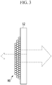
- FIG. 3 is an enlarged view of the second transparent window 12 in a laser crystallization device shown in FIG. 1 .
- the intensity of the laser beams propagating through the second transparent window 12 from inside the airtight container 10 is 100%, and the intensity of the laser beams reflected from the low reflection mirror 32 and propagating through the second transparent window 12 is about 10%.
- the laser crystallization device 100 alternates between a running state of outputting laser beams to the irradiation target and an idle state that is a standby state of waiting for a next output run.
- the running state and the idle state may be distinguished by whether an irradiation target is provided on the stage 63.
- FIG. 1 shows the laser crystallization device in a running state
- FIG. 2 shows the laser crystallization device in an idle state.
- the shutter 51 In a running state, the shutter 51 is moved away from the path of the laser beams (LB) to allow the laser beams (LBs) to propagate, and in the idle state, the shutter 51 is disposed to face the low reflection mirror 32.
- a voltage is maintained to the electrode 20 in the idle state so that the laser crystallization device 100 maintains a discharge.
- the cleaning mirror 40 is disposed between the second transparent window 12 and the low reflection mirror 32 to reflect the laser beams back through the second transparent window 12.
- the cleaning mirror 40 is a high reflection mirror with about 100% reflectivity. In the case the cleaning mirror 40 is a high reflection mirror, especially with about 100% reflectivity, the shutter 51 may be omitted.
- FIG. 4 is an enlarged view of the second transparent window 12 in a laser crystallization device shown in FIG. 2 .
- the cleaning mirror 40 in an idle state, reflects substantially 100% of the laser beams received through the second transparent window 12. Therefore, a laser impact with an intensity that is substantially the same as that of the laser impact on the second transparent window 12 from inside the airtight container 10 is applied to the second transparent window 12 from outside the airtight container 10 to remove the contaminated material 80 on the second transparent window 12.
- an excimer laser oscillates about every 600th of a second to about a 50th of a second, and a duration of the laser pulse is on the order of nanoseconds (ns).
- a duration of the laser pulse is on the order of nanoseconds (ns).
- the cleaning mirror 40 in an idle state, is disposed in the path of laser beams propagating through the second transparent window 12, and in a running state, it is moved away from the path of laser beams.
- the cleaning mirror 40 may be combined with a transfer device that can move the cleaning mirror 40.
- the transfer device may interlock or cooperate with a device for moving the shutter 51, and in this case, the cleaning mirror 40 and the shutter 51 move simultaneously.
- FIG. 5 is a schematic diagram of a cleaning mirror in a laser crystallization device shown in FIG. 1 .
- a transfer device 70A includes a driving motor 71, a rotation bar 72 combined with a rotation shaft of the driving motor 71, and a mirror frame 73 fixed to the rotation bar 72.
- the cleaning mirror 40 is fixed to the mirror frame 73, and its position is determined by a rotation direction and an angular displacement of the driving motor 71.
- the cleaning mirror 40 is disposed in the path of the laser beams in an idle state, referred to as a first position, and is moved out of the path of the laser beams in a running state, referred to as a second position.
- FIG. 5 illustrates a case in which the cleaning mirror 40 rotates by 90° in a clockwise direction to be disposed in the first position in an idle state, and rotates by 90° in a counterclockwise direction to be disposed in the second position in a running state.
- G. 6 is a schematic diagram of an exemplary variation of a transfer device shown in FIG. 5 .
- a transfer device 70B includes a driving motor 71 and a linear motion (LM) guide.
- the LM guide includes a rotation screw 74 combined with the driving motor 71, a slider 75 combined with the rotation screw 74, a mirror frame 73 fixed to the slider 75, and a rail 76 that guides the slider 75.
- the cleaning mirror 40 is fixed to the mirror frame 73.
- the slider 75 and the mirror frame 73 move on the rail 76 to move the cleaning mirror 40.
- a displacement direction and a displacement magnitude of the cleaning mirror 40 are determined by the rotation direction and the rotation magnitude of the driving motor 71.
- the cleaning mirror 40 is disposed in the first position in the path of the laser beams in an idle state, and it is disposed in the second position, away from the path of the laser beams, in a running state.
- FIG. 7 is a schematic diagram of an exemplary variation of a mirror frame shown in FIG. 6 .
- a mirror frame 731 of a transfer device 70C includes an opening 77 that is displaced from the cleaning mirror 40 in a direction parallel to the rail 76.
- the opening 77 is disposed in the path of the laser beams in a running state, and the cleaning mirror 40 is displaced by the slider 75 to be disposed in the path of the laser beams in an idle state.
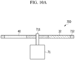
- FIG. 8 and FIG. 9 are schematic diagrams of a laser crystallization device according to another exemplary embodiment and FIG. 10A and FIG. 10B are schematic diagrams of a low reflection mirror and a cleaning mirror shown in FIG. 8 and FIG. 9 .
- a shutter 51 is also shown in the embodiments of FIGS. 8 and 9 , the shutter 51 may be omitted.
- a laser crystallization device 200 has the low reflection mirror 32 and the cleaning mirror 40 combined with a transfer device 70D, and one of the low reflection mirror 32 and the cleaning mirror 40 is disposed in the path of the laser beams by operation of the transfer device 70D.
- the transfer device 70D includes a driving motor 71 and a mirror frame 732 combined with a rotation shaft 711 of the driving motor 71.
- the mirror frame 732 is a circular plate, and the rotation shaft 711 is combined with a center of the mirror frame 732.
- the low reflection mirror 32 and the cleaning mirror 40 are fixed to the mirror frame 732, and are symmetrically disposed with respect to the rotation shaft 711.
- the low reflection mirror 32 in a running state, is disposed in the path of the laser beams, and the cleaning mirror 40 is moved away from the path of the laser beams.
- the mirror frame 732 rotates by 180° in a clockwise direction or counterclockwise direction. Therefore, the cleaning mirror 40 is disposed in the path of the laser beams, and the low reflection mirror 32 is moved away from the path of the laser beams.
- FIG. 11 is a schematic diagram of an exemplary variation of a transfer device shown in FIG. 10A and FIG. 10B .
- a transfer device 70E includes a driving motor 71 and an LM guide.
- the LM guide includes a rotation screw 74 combined with the driving motor 71, a slider 75 combined with the rotation screw 74, a mirror frame 733 fixed to the slider 75, and a rail 76 that guides the slider 75.
- the low reflection mirror 32 and the cleaning mirror 40 are fixed in the mirror frame 733 parallel to the rail 76.
- the slider 75 and the mirror frame 733 move on the rail 76 to move the low reflection mirror 32 and the cleaning mirror 40.
- the low reflection mirror 32 is disposed in the path of the laser beams that have propagated through the second transparent window 12, and the cleaning mirror 40 is moved away from the path of the laser beams.
- the cleaning mirror 40 is disposed in the path of the laser beams that have propagated through the second transparent window 12, and the low reflection mirror 32 is moved away from the path of the laser beams.
- the laser crystallization device 200 has a same configuration as an exemplary embodiment described with reference to FIGS. 1-7 except that the low reflection mirror 32 and the cleaning mirror 40 are fixed to a mirror frame to selectively face the second transparent window 12.
- contamination of the second transparent window 12 is reduced by the cleaning mirror 40 and a high transmittance can be maintained for a long duration. Therefore, a replacement period of the second transparent window 12 can be increased and an operational cost of the laser crystallization devices 100 and 200 can be reduced.
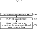
- FIG. 12 is a flowchart of a laser crystallization method according to an exemplary embodiment.
- a laser crystallization method includes a first step S10 of exciting a gas medium in an airtight container to generate laser beams, a second step S20 of transmitting the laser beams through a first transparent window and a second transparent window fixed to respective end portions of the airtight container, amplifying the laser beams using a high reflection mirror and a low reflection mirror, and outputting the amplified laser beams, and a third step S30 of disposing a cleaning mirror in a path of the laser beams that have propagated through the second transparent window.
- laser beams are generated in the first step S10.
- a pair of electrodes 20 are disposed in the airtight container 10. One of the pair of electrodes 20 is grounded and the other thereof is connected to the high-voltage power supply 21.
- a voltage is applied to the connected electrode 20, and discharging begins in the space between the pair of electrodes 20 that excites the gas medium to generate laser beams.
- laser beams are output during the second step S20.
- the high reflection mirror 31 is disposed outside the first transparent window 11, and the low reflection mirror 32 is disposed outside the second transparent window 12.
- the laser beams being reflected between the high reflection mirror 31 and the low reflection mirror 32 generate resonance and are amplified, and the amplified laser beams propagate through the low reflection mirror 32 to be output to the irradiation target.
- the first step S10 and the second step S20 occur substantially simultaneously.
- the irradiation target is an amorphous silicon layer
- the amorphous silicon layer is annealed into a polycrystalline silicon layer by irradiation of the laser beams.
- the second step S20 is the running state in which laser beams are irradiated to the irradiation target.
- the cleaning mirror is disposed in the third step S30.
- the third step S30 is the idle state, that is, a standby state for the next output run, and the second step S20 and the third step S30 are alternately and repeatedly performed.
- the cleaning mirror 40 is disposed to face the second transparent window 12.
- the cleaning mirror 40 is a high reflection mirror with almost 100% reflectivity, and it reflects the laser beams that have propagated through the second transparent window 12 back to the second transparent window 12 to remove the contamination material 80 attached to the internal side of the second transparent window 12.
- the cleaning mirror 40 is combined with the transfer device and can be displaced by the transfer device.
- the cleaning mirror 40 is moved away from and out of the path of the laser beams during the second step S20, and displaced by the transfer device to be disposed between the second transparent window 12 and the low reflection mirror 32 in the third step S30.
- the transfer device may have one of the configurations of FIG. 5 , FIG. 6 , or FIG. 7 .
- the cleaning mirror 40 and the low reflection mirror 32 are combined with the transfer device and can be displaced by the transfer device.
- the transfer device disposes one of the cleaning mirror 40 or the low reflection mirror 32 in the path of the laser beams.
- the low reflection mirror 32 is disposed in the path of the laser beams, and the cleaning mirror 40 is disposed out of the path of the laser beams.
- the transfer device exchanges positions of the low reflection mirror 32 and the cleaning mirror 40 so that the cleaning mirror 40 is disposed in the path of the laser beams.
- the transfer device may have one of the configurations of FIG. 10A , FIG. 10B , or FIG. 11 .
- the impurities that were absorbed into the second transparent window 12 during the second step S20 are removed by the laser beams reflected from the cleaning mirror 40 in the third step S30, and the contaminates are removed from the second transparent window 12.
- FIG. 13 and FIG. 14 are graphs of transmittance as a function of wavelength of a second transparent window of a laser crystallization device according to a comparative example and a laser crystallization device according to an exemplary embodiment
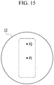
- FIG. 15 is a front view of a second transparent window for locating a point for measuring transmittance.
- FIG. 13 shows a result of measuring transmittance at a center point of a second transparent window
- FIG. 14 shows a result of measuring transmittance at a surrounding point of a second transparent window
- P1 represents a center point
- P2 represents a surrounding point
- the surrounding point P2 is a point halfway between the center point P1 and an edge of the second transparent window 12, and a dotted line outlines a region in the second transparent window 12 through which laser beams are actually transmitted.
- the comparative example is a case when the cleaning mirror is not used, and in both the comparative example and an exemplary embodiment, transmittance of the second transparent window is measured after irradiation of forty million shots.
- Output characteristics of the laser beams of the comparative example and an exemplary embodiment are 1.6 kV and 200 Hz.
- transmittance of a 308 nm wavelength laser beam through the second transparent window is 93.7% in the comparative example, and is 98.0% in an exemplary embodiment.
- transmittance of the 308 nm wavelength laser beam through the second transparent window is 90.7% in the comparative example, and is 96.1% in the exemplary embodiment.
- An exemplary embodiment that uses a cleaning mirror has a 5% transmittance improvement as compared to the comparative example.
Landscapes
- Physics & Mathematics (AREA)
- Electromagnetism (AREA)
- Optics & Photonics (AREA)
- Engineering & Computer Science (AREA)
- Plasma & Fusion (AREA)
- Chemical & Material Sciences (AREA)
- General Physics & Mathematics (AREA)
- Chemical Kinetics & Catalysis (AREA)
- Crystallography & Structural Chemistry (AREA)
- Materials Engineering (AREA)
- Thermal Sciences (AREA)
- Metallurgy (AREA)
- Organic Chemistry (AREA)
- Condensed Matter Physics & Semiconductors (AREA)
- Mechanical Engineering (AREA)
- Oil, Petroleum & Natural Gas (AREA)
- General Chemical & Material Sciences (AREA)
- Recrystallisation Techniques (AREA)
- Lasers (AREA)
- Health & Medical Sciences (AREA)
- Toxicology (AREA)
- Physical Or Chemical Processes And Apparatus (AREA)
Claims (12)
- Laserkristallisationsverfahren, umfassend:Anregen eines Gasmediums in einem luftdichten Behälter (10), wobei Laserstrahlen erzeugt werden;Verstärken der Laserstrahlen durch Reflektieren der Laserstrahlen zwischen einem stark reflektierendem Spiegel (31) und einem schwach reflektierenden Spiegel (32), die jeweils gegenüberliegenden Endabschnitten des luftdichten Behälter (10) zugewandt angeordnet sind, wobei ein erstes transparentes Fenster (11) und ein zweites transparentes Fenster (12) an jeweiligen Endabschnitten des luftdichten Behälters (10) befestigt sind, und Ausgeben der verstärkten Laserstrahlen;gekennzeichnet durchAnordnen eines Reinigungsspiegels (40) in einem Weg der Laserstrahlen, die sich durch das zweite transparente Fenster (12) ausgebreitet haben, um Verunreinigungen auf dem zweiten transparenten Fenster (12) zu entfernen, indem alle Laserstrahlen, die sich durch das zweite transparente Fenster (12) ausgebreitet haben, durch das zweite transparente Fenster (12) zurückreflektiert werdenwobei der Reinigungsspiegel (40) während des Ausgebens der verstärkten Laserstrahlen von dem Weg der Laserstrahlen entfernt positioniert ist; undwobei der Reinigungsspiegel (40) mit einer Transfervorrichtung (70A, 70B, 70C, 70D, 70E) kombiniert ist, die den Reinigungsspiegel (40) zwischen einer ersten Position in dem Weg der Laserstrahlen und einer zweiten Position von dem Weg der Laserstrahlen entfernt und außerhalb von diesem verlagert;die Transfervorrichtung (70A, 70D; 70B, 70C, 70E) einen Antriebsmotor (71) und einen Spiegelrahmen (73, 732, 731, 733) beinhaltet, der abgelenkt oder linear von dem Antriebsmotor (71) verlagert wird und der den Reinigungsspiegel (40) befestigt, undder Reinigungsspiegel (40) zwischen der ersten Position und der zweiten Position durch Ablenkung beziehungsweise lineare Bewegung des Spiegelrahmens (73, 732, 731, 733) verlagert wird.
- Laserkristallisationsverfahren nach Anspruch 1, wobei
das Ausgeben der verstärkten Laserstrahlen ein Betriebszustand ist, wobei die Laserstrahlen auf ein Strahlungsziel gestrahlt werden, und das Anordnen des Reinigungsspiegels (40) ein Ruhezustand des Wartens auf einen nächsten Ausgabedurchlauf ist. - Laserkristallisationsverfahren nach Anspruch 1, wobei
der schwach reflektierende Spiegel (32) und der Reinigungsspiegel (40) mit der Transfervorrichtung (70D, 70E) kombiniert sind, die die Positionen von diesen zwischen dem Ausgeben der verstärkten Laserstrahlen und dem Anordnen des Reinigungsspiegels (40) wechselt. - Laserkristallisationsverfahren nach Anspruch 3, wobei
die Transfervorrichtung (70D) einen Antriebsmotor (71) und einen Spiegelrahmen (732) beinhaltet, der durch den Antriebsmotor (71) gedreht wird und der den schwach reflektierenden Spiegel (32) und den Reinigungsspiegel (40) befestigt, und
die Positionen des schwach reflektierenden Spiegels (32) und des Reinigungsspiegels (40) durch Drehen des Spiegelrahmens (732) gewechselt werden. - Laserkristallisationsverfahren nach Anspruch 1, wobei
der schwach reflektierende Spiegel (32) und der Reinigungsspiegel (40) mit der Transfervorrichtung (70D, 70E) kombiniert sind, und
der schwach reflektierende Spiegel (32) von dem Weg der Laserstrahlen wegbewegt wird, wenn der Reinigungsspiegel (40) angeordnet wird. - Laserkristallisationsverfahren nach Anspruch 5, wobei
die Transfervorrichtung (70E) einen Antriebsmotor (71) und einen Spiegelrahmen (733) beinhaltet, der linear von dem Antriebsmotor (71) verschoben wird und der den schwach reflektierenden Spiegel (32) und den Reinigungsspiegel (40) befestigt, und
einer des schwach reflektierenden Spiegels (32) und des Reinigungsspiegels (40) durch lineare Verschiebung des Spiegelrahmens (733) derart angeordnet wird, dass er dem zweiten transparenten Fenster (12) zugewandt ist. - Laserkristallisationsvorrichtung, umfassend:einen luftdichten Behälter (10), bei dem es sich um eine Gaslaservorrichtung handelt, die mit einem Gasmedium befüllt ist, ein erstes transparentes Fenster (11) und ein zweites transparentes Fenster (12), die an jeweiligen Endabschnitten des luftdichten Behälters (10) befestigt sind, die einander entlang einer Mittelachse des luftdichten Behälters (10) zugewandt sind;einen stark reflektierenden Spiegel (31), der außerhalb des ersten transparenten Fensters (11) installiert ist und einen schwach reflektierenden Spiegel (32), der außerhalb des zweiten transparenten Fensters (12) installiert ist, wobei der schwach reflektierende Spiegel (32) eine Reflektivität aufweist, die geringer als seine Durchlässigkeit ist, gekennzeichnet durcheinen Reinigungsspiegel (40) wobei die Laserkristallisationsvorrichtung derart angepasst ist, dasswährend eines Betriebszustands Laserstrahlen von dem luftdichten Behälter (10) durch das zweite transparente Fenster (12) und den schwach reflektierenden Spiegel (32) zu einem Strahlungsziel ausgegeben werden, und der Reinigungsspiegel (40) entfernt von einem Weg der Laserstrahlen, die von dem luftdichten Behälter (10) ausgegeben werden, und außerhalb von diesem positioniert ist, undwährend eines Ruhezustands der Reinigungsspiegel (40) in dem Weg der Laserstrahlen, die von dem luftdichten Behälter (10) ausgegeben werden, angeordnet ist, wobei die Laserstrahlen in den luftdichten Behälter (10) zurückreflektiert werden, um Verunreinigungen auf dem zweiten transparenten Fenster (12) zu entfernen, indem alle Laserstrahlen, die sich durch das zweite transparente Fenster (12) ausgebreitet haben, durch das zweite transparente Fenster (12) zurückreflektiert werden ferner umfassend eine Blende (51), die die Übertragung von Laserstrahlen, die sich im Betriebszustand durch den schwach reflektierenden Spiegel (32) ausbreiten, zulässt und Laserstrahlen, die sich im Ruhezustand durch den schwach reflektierenden Spiegel (32) ausbreiten, blockiert;wobei der schwach reflektierende Spiegel (32) und der Reinigungsspiegel (40) mit einer Transfervorrichtung (70D, 70E) kombiniert sind, und einer von dem schwach reflektierenden Spiegel (32) und dem Reinigungsspiegel (40) durch den Betrieb der Transfervorrichtung (70D, 70E) in dem Weg der Laserstrahlen angeordnet wird;dadurch gekennzeichnet, dassdie Transfervorrichtung (70D; 70E) einen Antriebsmotor (71) und einen Spiegelrahmen (732; 733) beinhaltet, der von dem Antriebsmotor (71) gedreht oder linear verschoben wird und der den schwach reflektierenden Spiegel (32) und den Reinigungsspiegel (40) befestigt, undeiner von dem schwach reflektierenden Spiegel (32) und dem Reinigungsspiegel (40) angeordnet ist, um dem zweiten transparenten Fenster (12) zugewandt zu sein, indem der Spiegelrahmen (732; 733) abgelenkt beziehungsweise linear verschoben wird.
- Laserkristallisationsvorrichtung nach Anspruch 7, wobei
der Reinigungsspiegel (40) mit einer Transfervorrichtung (70A, 70B, 70C, 70D, 70E) kombiniert ist, die den Reinigungsspiegel (40) zwischen einer ersten Position in dem Weg der Laserstrahlen und einer zweiten Position von dem Weg der Laserstrahlen entfernt und außerhalb von diesem bewegt. - Laserkristallisationsvorrichtung nach Anspruch 8, wobei
die Transfervorrichtung (70A, 70D) einen Antriebsmotor (71) und einen Spiegelrahmen (73, 732) beinhaltet, der durch den Antriebsmotor (71) gedreht wird und der den Reinigungsspiegel (40) befestigt, und
der Reinigungsspiegel (40) zwischen der ersten Position und der zweiten Position durch Drehen des Spiegelrahmens (73, 732) verlagert wird. - Laserkristallisationsvorrichtung nach Anspruch 8, wobei
die Transfervorrichtung (70B, 70C, 70E) einen Antriebsmotor (71) und einen Spiegelrahmen (73, 731, 733) beinhaltet, der von dem Antriebsmotor (71) linear verlagert wird und der den Reinigungsspiegel (40) befestigt, und
der Reinigungsspiegel (40) zwischen der ersten Position und der zweiten Position durch lineare Bewegung des Spiegelrahmens (73, 731, 733) verlagert wird. - Laserkristallisationsvorrichtung nach wenigstens einem der Ansprüche 7 bis 10, wobei die Laserkristallisationsvorrichtung derart angepasst ist, dass die Laserstrahlen, die in den luftdichten Behälter (10) zurückreflektiert werden, Verunreinigungsmaterial (80) entfernen, dass ein einer Innenseite des zweiten transparenten Fensters (12) haftet.
- Laserkristallisationsvorrichtung nach wenigstens einem der Ansprüche 7 bis 11, ferner umfassend:ein Paar von Elektroden (20), die in Bezug auf die Mittelachse des luftdichten Behälters (10) symmetrisch angeordnet sind, wobei das Gasmedium angeregt wird, um Laserstrahlen zu erzeugen, wenn eine Spannung an die Elektroden (20) angelegt wird;eine Hochspannungsstromversorgung (21), die mit einer von dem Paar von Elektroden (20) verbunden ist;einen reflektierenden Spiegel (52), der eine Ausbreitungsrichtung der Laserstrahlen ändert; undeine Kondensorlinse (53), die die Laserstrahlen auf das Strahlungsziel kondensiert.
Applications Claiming Priority (1)
| Application Number | Priority Date | Filing Date | Title |
|---|---|---|---|
| KR1020160073882A KR102486989B1 (ko) | 2016-06-14 | 2016-06-14 | 레이저 결정화 장치 및 레이저 결정화 방법 |
Publications (2)
| Publication Number | Publication Date |
|---|---|
| EP3258554A1 EP3258554A1 (de) | 2017-12-20 |
| EP3258554B1 true EP3258554B1 (de) | 2019-08-07 |
Family
ID=59061881
Family Applications (1)
| Application Number | Title | Priority Date | Filing Date |
|---|---|---|---|
| EP17175915.2A Active EP3258554B1 (de) | 2016-06-14 | 2017-06-14 | Laserkristallisierungsverfahren und -vorrichtung |
Country Status (4)
| Country | Link |
|---|---|
| US (1) | US11087980B2 (de) |
| EP (1) | EP3258554B1 (de) |
| KR (1) | KR102486989B1 (de) |
| CN (1) | CN107498194B (de) |
Families Citing this family (4)
| Publication number | Priority date | Publication date | Assignee | Title |
|---|---|---|---|---|
| KR102622712B1 (ko) * | 2017-10-13 | 2024-01-08 | 더 트러스티이스 오브 콜롬비아 유니버시티 인 더 시티 오브 뉴욕 | 스팟 빔 및 라인 빔 결정화를 위한 시스템들 및 방법들 |
| US11128097B2 (en) * | 2019-08-02 | 2021-09-21 | Samsung Electronics Co., Ltd. | Light source apparatus |
| KR102733491B1 (ko) * | 2019-08-26 | 2024-11-22 | 삼성디스플레이 주식회사 | 레이저 광원 및 레이저 결정화 장치 |
| KR20240110165A (ko) | 2023-01-05 | 2024-07-15 | 삼성디스플레이 주식회사 | 윈도우, 이를 포함하는 표시 장치 및 윈도우의 제조방법 |
Family Cites Families (24)
| Publication number | Priority date | Publication date | Assignee | Title |
|---|---|---|---|---|
| US3624531A (en) * | 1969-09-05 | 1971-11-30 | Westinghouse Electric Corp | Laser resonator assemblage |
| JPS6047485A (ja) * | 1983-08-25 | 1985-03-14 | Nec Corp | ガスレ−ザ装置 |
| JPS639172A (ja) * | 1986-06-30 | 1988-01-14 | Komatsu Ltd | 縦型レ−ザヘツド |
| JPS63209187A (ja) | 1987-02-26 | 1988-08-30 | Nikon Corp | エキシマレ−ザ装置 |
| JPH01117381A (ja) * | 1987-10-30 | 1989-05-10 | Shimadzu Corp | エキシマレーザ用光共振器 |
| JP2844787B2 (ja) * | 1990-01-18 | 1999-01-06 | 日本電気株式会社 | 光学窓遮蔽機構付チャンバ |
| US5091913A (en) * | 1990-04-10 | 1992-02-25 | Tsinghua Unversity | Quartz crystal tuning he-ne double frequency laser |
| JP2599286Y2 (ja) | 1993-01-12 | 1999-08-30 | 株式会社小松製作所 | ガスレーザ装置のウインド機構 |
| JPH06237034A (ja) | 1993-02-10 | 1994-08-23 | Nec Corp | 放電励起ガスレーザ装置 |
| US5805625A (en) * | 1994-02-09 | 1998-09-08 | Walter Langner | Laser |
| WO1998007022A1 (en) | 1996-08-16 | 1998-02-19 | Imaging Research, Inc. | A digital imaging system for assays in well plates, gels and blots |
| US7006541B2 (en) * | 1998-06-01 | 2006-02-28 | Lambda Physik Ag | Absolute wavelength calibration of lithography laser using multiple element or tandem see through hollow cathode lamp |
| US7039086B2 (en) * | 2001-04-09 | 2006-05-02 | Cymer, Inc. | Control system for a two chamber gas discharge laser |
| US6768765B1 (en) * | 2001-06-07 | 2004-07-27 | Lambda Physik Ag | High power excimer or molecular fluorine laser system |
| JP4397571B2 (ja) * | 2001-09-25 | 2010-01-13 | 株式会社半導体エネルギー研究所 | レーザ照射方法およびレーザ照射装置、並びに半導体装置の作製方法 |
| US6970492B2 (en) | 2002-05-17 | 2005-11-29 | Lambda Physik Ag | DUV and VUV laser with on-line pulse energy monitor |
| DE10252443A1 (de) * | 2002-11-12 | 2004-05-27 | Trumpf Lasertechnik Gmbh | Vorrichtung zur Ablenkung eines Laserstrahls |
| KR20040066308A (ko) | 2003-01-17 | 2004-07-27 | 삼성전자주식회사 | 노광용 레이저 장치의 부분반사 미러 |
| US20050041697A1 (en) * | 2003-06-12 | 2005-02-24 | Martin Seifert | Portable laser |
| JP4182034B2 (ja) * | 2004-08-05 | 2008-11-19 | ファナック株式会社 | 切断加工用レーザ装置 |
| JP2006344908A (ja) | 2005-06-10 | 2006-12-21 | Sumitomo Heavy Ind Ltd | レーザ発振器及びレーザ発振器の運転方法 |
| JP5630758B2 (ja) * | 2006-08-09 | 2014-11-26 | 株式会社小松製作所 | エキシマレーザ装置 |
| KR101164063B1 (ko) | 2009-10-27 | 2012-07-12 | 주식회사 케이씨텍 | 레이저 세정장치 |
| JP5820689B2 (ja) * | 2011-10-28 | 2015-11-24 | ギガフォトン株式会社 | レーザ装置 |
-
2016
- 2016-06-14 KR KR1020160073882A patent/KR102486989B1/ko active Active
-
2017
- 2017-03-22 US US15/466,330 patent/US11087980B2/en active Active
- 2017-06-14 CN CN201710447134.1A patent/CN107498194B/zh active Active
- 2017-06-14 EP EP17175915.2A patent/EP3258554B1/de active Active
Non-Patent Citations (1)
| Title |
|---|
| None * |
Also Published As
| Publication number | Publication date |
|---|---|
| CN107498194B (zh) | 2021-07-09 |
| EP3258554A1 (de) | 2017-12-20 |
| KR102486989B1 (ko) | 2023-01-10 |
| US20170358449A1 (en) | 2017-12-14 |
| US11087980B2 (en) | 2021-08-10 |
| CN107498194A (zh) | 2017-12-22 |
| KR20170141310A (ko) | 2017-12-26 |
Similar Documents
| Publication | Publication Date | Title |
|---|---|---|
| US6847006B2 (en) | Laser annealing apparatus and semiconductor device manufacturing method | |
| US11087980B2 (en) | Laser crystallization device | |
| TWI389352B (zh) | 雷射輻射方法、和使用該雷射輻射方法製造半導體裝置的方法 | |
| US8446924B2 (en) | Laser annealing method and apparatus | |
| KR101357017B1 (ko) | 레이저 결정화 장치 | |
| US7795154B2 (en) | Method for manufacturing semiconductor device that uses laser ablation, to selectively remove one or more material layers | |
| CN109979805A (zh) | 通过光纤激光器使非晶硅衬底均匀再结晶的工艺和系统 | |
| CN101303969B (zh) | 照射设备、半导体制造设备与方法和显示装置制造方法 | |
| CN112510474B (zh) | 激光光源和包括该激光光源的激光晶化设备 | |
| US9966721B2 (en) | Laser system | |
| JP2005340788A (ja) | レーザ照射方法およびそれを用いた半導体装置の作製方法 | |
| US20170248782A1 (en) | Laser irradiation device | |
| KR20180131667A (ko) | 고체 레이저 결정화 장치 | |
| US20160172814A1 (en) | Laser unit and extreme ultraviolet light generating system | |
| JP4944705B2 (ja) | 半導体装置の作製方法及び配線の作製方法 | |
| JP4602023B2 (ja) | 半導体装置の作製方法 | |
| JP2005109460A (ja) | レーザ照射装置、レーザ照射方法及び半導体装置の作製方法 | |
| KR20200140961A (ko) | 레이저 결정화 시스템 및 레이저 결정화 방법 | |
| JP2003203876A (ja) | レーザ照射装置 | |
| US20070278193A1 (en) | Device and method to create a low divergence, high power laser beam for material processing applications | |
| US20210366710A1 (en) | Method for manufacturing semiconductor crystalline thin film and laser annealing system | |
| CN120076687A (zh) | 用于制造显示装置的设备 | |
| JP2003203877A (ja) | レーザ照射方法および半導体装置の作製方法 | |
| KR20070062797A (ko) | 실리콘 결정화 장치 |
Legal Events
| Date | Code | Title | Description |
|---|---|---|---|
| PUAI | Public reference made under article 153(3) epc to a published international application that has entered the european phase |
Free format text: ORIGINAL CODE: 0009012 |
|
| STAA | Information on the status of an ep patent application or granted ep patent |
Free format text: STATUS: THE APPLICATION HAS BEEN PUBLISHED |
|
| AK | Designated contracting states |
Kind code of ref document: A1 Designated state(s): AL AT BE BG CH CY CZ DE DK EE ES FI FR GB GR HR HU IE IS IT LI LT LU LV MC MK MT NL NO PL PT RO RS SE SI SK SM TR |
|
| AX | Request for extension of the european patent |
Extension state: BA ME |
|
| STAA | Information on the status of an ep patent application or granted ep patent |
Free format text: STATUS: REQUEST FOR EXAMINATION WAS MADE |
|
| 17P | Request for examination filed |
Effective date: 20180620 |
|
| RBV | Designated contracting states (corrected) |
Designated state(s): AL AT BE BG CH CY CZ DE DK EE ES FI FR GB GR HR HU IE IS IT LI LT LU LV MC MK MT NL NO PL PT RO RS SE SI SK SM TR |
|
| GRAP | Despatch of communication of intention to grant a patent |
Free format text: ORIGINAL CODE: EPIDOSNIGR1 |
|
| STAA | Information on the status of an ep patent application or granted ep patent |
Free format text: STATUS: GRANT OF PATENT IS INTENDED |
|
| RIC1 | Information provided on ipc code assigned before grant |
Ipc: H01S 3/034 20060101AFI20190118BHEP |
|
| INTG | Intention to grant announced |
Effective date: 20190221 |
|
| GRAS | Grant fee paid |
Free format text: ORIGINAL CODE: EPIDOSNIGR3 |
|
| GRAA | (expected) grant |
Free format text: ORIGINAL CODE: 0009210 |
|
| STAA | Information on the status of an ep patent application or granted ep patent |
Free format text: STATUS: THE PATENT HAS BEEN GRANTED |
|
| AK | Designated contracting states |
Kind code of ref document: B1 Designated state(s): AL AT BE BG CH CY CZ DE DK EE ES FI FR GB GR HR HU IE IS IT LI LT LU LV MC MK MT NL NO PL PT RO RS SE SI SK SM TR |
|
| REG | Reference to a national code |
Ref country code: GB Ref legal event code: FG4D |
|
| REG | Reference to a national code |
Ref country code: CH Ref legal event code: EP Ref country code: AT Ref legal event code: REF Ref document number: 1165274 Country of ref document: AT Kind code of ref document: T Effective date: 20190815 |
|
| REG | Reference to a national code |
Ref country code: DE Ref legal event code: R096 Ref document number: 602017005838 Country of ref document: DE |
|
| REG | Reference to a national code |
Ref country code: IE Ref legal event code: FG4D |
|
| REG | Reference to a national code |
Ref country code: NL Ref legal event code: MP Effective date: 20190807 |
|
| REG | Reference to a national code |
Ref country code: LT Ref legal event code: MG4D |
|
| PG25 | Lapsed in a contracting state [announced via postgrant information from national office to epo] |
Ref country code: FI Free format text: LAPSE BECAUSE OF FAILURE TO SUBMIT A TRANSLATION OF THE DESCRIPTION OR TO PAY THE FEE WITHIN THE PRESCRIBED TIME-LIMIT Effective date: 20190807 Ref country code: NO Free format text: LAPSE BECAUSE OF FAILURE TO SUBMIT A TRANSLATION OF THE DESCRIPTION OR TO PAY THE FEE WITHIN THE PRESCRIBED TIME-LIMIT Effective date: 20191107 Ref country code: PT Free format text: LAPSE BECAUSE OF FAILURE TO SUBMIT A TRANSLATION OF THE DESCRIPTION OR TO PAY THE FEE WITHIN THE PRESCRIBED TIME-LIMIT Effective date: 20191209 Ref country code: SE Free format text: LAPSE BECAUSE OF FAILURE TO SUBMIT A TRANSLATION OF THE DESCRIPTION OR TO PAY THE FEE WITHIN THE PRESCRIBED TIME-LIMIT Effective date: 20190807 Ref country code: BG Free format text: LAPSE BECAUSE OF FAILURE TO SUBMIT A TRANSLATION OF THE DESCRIPTION OR TO PAY THE FEE WITHIN THE PRESCRIBED TIME-LIMIT Effective date: 20191107 Ref country code: HR Free format text: LAPSE BECAUSE OF FAILURE TO SUBMIT A TRANSLATION OF THE DESCRIPTION OR TO PAY THE FEE WITHIN THE PRESCRIBED TIME-LIMIT Effective date: 20190807 Ref country code: LT Free format text: LAPSE BECAUSE OF FAILURE TO SUBMIT A TRANSLATION OF THE DESCRIPTION OR TO PAY THE FEE WITHIN THE PRESCRIBED TIME-LIMIT Effective date: 20190807 Ref country code: NL Free format text: LAPSE BECAUSE OF FAILURE TO SUBMIT A TRANSLATION OF THE DESCRIPTION OR TO PAY THE FEE WITHIN THE PRESCRIBED TIME-LIMIT Effective date: 20190807 |
|
| REG | Reference to a national code |
Ref country code: AT Ref legal event code: MK05 Ref document number: 1165274 Country of ref document: AT Kind code of ref document: T Effective date: 20190807 |
|
| PG25 | Lapsed in a contracting state [announced via postgrant information from national office to epo] |
Ref country code: RS Free format text: LAPSE BECAUSE OF FAILURE TO SUBMIT A TRANSLATION OF THE DESCRIPTION OR TO PAY THE FEE WITHIN THE PRESCRIBED TIME-LIMIT Effective date: 20190807 Ref country code: LV Free format text: LAPSE BECAUSE OF FAILURE TO SUBMIT A TRANSLATION OF THE DESCRIPTION OR TO PAY THE FEE WITHIN THE PRESCRIBED TIME-LIMIT Effective date: 20190807 Ref country code: AL Free format text: LAPSE BECAUSE OF FAILURE TO SUBMIT A TRANSLATION OF THE DESCRIPTION OR TO PAY THE FEE WITHIN THE PRESCRIBED TIME-LIMIT Effective date: 20190807 Ref country code: GR Free format text: LAPSE BECAUSE OF FAILURE TO SUBMIT A TRANSLATION OF THE DESCRIPTION OR TO PAY THE FEE WITHIN THE PRESCRIBED TIME-LIMIT Effective date: 20191108 Ref country code: IS Free format text: LAPSE BECAUSE OF FAILURE TO SUBMIT A TRANSLATION OF THE DESCRIPTION OR TO PAY THE FEE WITHIN THE PRESCRIBED TIME-LIMIT Effective date: 20191207 |
|
| PG25 | Lapsed in a contracting state [announced via postgrant information from national office to epo] |
Ref country code: TR Free format text: LAPSE BECAUSE OF FAILURE TO SUBMIT A TRANSLATION OF THE DESCRIPTION OR TO PAY THE FEE WITHIN THE PRESCRIBED TIME-LIMIT Effective date: 20190807 |
|
| PG25 | Lapsed in a contracting state [announced via postgrant information from national office to epo] |
Ref country code: PL Free format text: LAPSE BECAUSE OF FAILURE TO SUBMIT A TRANSLATION OF THE DESCRIPTION OR TO PAY THE FEE WITHIN THE PRESCRIBED TIME-LIMIT Effective date: 20190807 Ref country code: RO Free format text: LAPSE BECAUSE OF FAILURE TO SUBMIT A TRANSLATION OF THE DESCRIPTION OR TO PAY THE FEE WITHIN THE PRESCRIBED TIME-LIMIT Effective date: 20190807 Ref country code: IT Free format text: LAPSE BECAUSE OF FAILURE TO SUBMIT A TRANSLATION OF THE DESCRIPTION OR TO PAY THE FEE WITHIN THE PRESCRIBED TIME-LIMIT Effective date: 20190807 Ref country code: AT Free format text: LAPSE BECAUSE OF FAILURE TO SUBMIT A TRANSLATION OF THE DESCRIPTION OR TO PAY THE FEE WITHIN THE PRESCRIBED TIME-LIMIT Effective date: 20190807 Ref country code: DK Free format text: LAPSE BECAUSE OF FAILURE TO SUBMIT A TRANSLATION OF THE DESCRIPTION OR TO PAY THE FEE WITHIN THE PRESCRIBED TIME-LIMIT Effective date: 20190807 Ref country code: EE Free format text: LAPSE BECAUSE OF FAILURE TO SUBMIT A TRANSLATION OF THE DESCRIPTION OR TO PAY THE FEE WITHIN THE PRESCRIBED TIME-LIMIT Effective date: 20190807 |
|
| PG25 | Lapsed in a contracting state [announced via postgrant information from national office to epo] |
Ref country code: SK Free format text: LAPSE BECAUSE OF FAILURE TO SUBMIT A TRANSLATION OF THE DESCRIPTION OR TO PAY THE FEE WITHIN THE PRESCRIBED TIME-LIMIT Effective date: 20190807 Ref country code: SM Free format text: LAPSE BECAUSE OF FAILURE TO SUBMIT A TRANSLATION OF THE DESCRIPTION OR TO PAY THE FEE WITHIN THE PRESCRIBED TIME-LIMIT Effective date: 20190807 Ref country code: IS Free format text: LAPSE BECAUSE OF FAILURE TO SUBMIT A TRANSLATION OF THE DESCRIPTION OR TO PAY THE FEE WITHIN THE PRESCRIBED TIME-LIMIT Effective date: 20200224 Ref country code: CZ Free format text: LAPSE BECAUSE OF FAILURE TO SUBMIT A TRANSLATION OF THE DESCRIPTION OR TO PAY THE FEE WITHIN THE PRESCRIBED TIME-LIMIT Effective date: 20190807 |
|
| REG | Reference to a national code |
Ref country code: DE Ref legal event code: R097 Ref document number: 602017005838 Country of ref document: DE |
|
| PLBE | No opposition filed within time limit |
Free format text: ORIGINAL CODE: 0009261 |
|
| STAA | Information on the status of an ep patent application or granted ep patent |
Free format text: STATUS: NO OPPOSITION FILED WITHIN TIME LIMIT |
|
| PG2D | Information on lapse in contracting state deleted |
Ref country code: IS |
|
| 26N | No opposition filed |
Effective date: 20200603 |
|
| PG25 | Lapsed in a contracting state [announced via postgrant information from national office to epo] |
Ref country code: SI Free format text: LAPSE BECAUSE OF FAILURE TO SUBMIT A TRANSLATION OF THE DESCRIPTION OR TO PAY THE FEE WITHIN THE PRESCRIBED TIME-LIMIT Effective date: 20190807 |
|
| PG25 | Lapsed in a contracting state [announced via postgrant information from national office to epo] |
Ref country code: ES Free format text: LAPSE BECAUSE OF FAILURE TO SUBMIT A TRANSLATION OF THE DESCRIPTION OR TO PAY THE FEE WITHIN THE PRESCRIBED TIME-LIMIT Effective date: 20190807 |
|
| PG25 | Lapsed in a contracting state [announced via postgrant information from national office to epo] |
Ref country code: MC Free format text: LAPSE BECAUSE OF FAILURE TO SUBMIT A TRANSLATION OF THE DESCRIPTION OR TO PAY THE FEE WITHIN THE PRESCRIBED TIME-LIMIT Effective date: 20190807 |
|
| REG | Reference to a national code |
Ref country code: CH Ref legal event code: PL |
|
| PG25 | Lapsed in a contracting state [announced via postgrant information from national office to epo] |
Ref country code: LU Free format text: LAPSE BECAUSE OF NON-PAYMENT OF DUE FEES Effective date: 20200614 |
|
| REG | Reference to a national code |
Ref country code: BE Ref legal event code: MM Effective date: 20200630 |
|
| PG25 | Lapsed in a contracting state [announced via postgrant information from national office to epo] |
Ref country code: LI Free format text: LAPSE BECAUSE OF NON-PAYMENT OF DUE FEES Effective date: 20200630 Ref country code: CH Free format text: LAPSE BECAUSE OF NON-PAYMENT OF DUE FEES Effective date: 20200630 Ref country code: IE Free format text: LAPSE BECAUSE OF NON-PAYMENT OF DUE FEES Effective date: 20200614 |
|
| PG25 | Lapsed in a contracting state [announced via postgrant information from national office to epo] |
Ref country code: BE Free format text: LAPSE BECAUSE OF NON-PAYMENT OF DUE FEES Effective date: 20200630 |
|
| PG25 | Lapsed in a contracting state [announced via postgrant information from national office to epo] |
Ref country code: MT Free format text: LAPSE BECAUSE OF FAILURE TO SUBMIT A TRANSLATION OF THE DESCRIPTION OR TO PAY THE FEE WITHIN THE PRESCRIBED TIME-LIMIT Effective date: 20190807 Ref country code: CY Free format text: LAPSE BECAUSE OF FAILURE TO SUBMIT A TRANSLATION OF THE DESCRIPTION OR TO PAY THE FEE WITHIN THE PRESCRIBED TIME-LIMIT Effective date: 20190807 |
|
| PG25 | Lapsed in a contracting state [announced via postgrant information from national office to epo] |
Ref country code: MK Free format text: LAPSE BECAUSE OF FAILURE TO SUBMIT A TRANSLATION OF THE DESCRIPTION OR TO PAY THE FEE WITHIN THE PRESCRIBED TIME-LIMIT Effective date: 20190807 |
|
| P01 | Opt-out of the competence of the unified patent court (upc) registered |
Effective date: 20230516 |
|
| PGFP | Annual fee paid to national office [announced via postgrant information from national office to epo] |
Ref country code: GB Payment date: 20260526 Year of fee payment: 10 |
|
| PGFP | Annual fee paid to national office [announced via postgrant information from national office to epo] |
Ref country code: DE Payment date: 20260520 Year of fee payment: 10 |
|
| PGFP | Annual fee paid to national office [announced via postgrant information from national office to epo] |
Ref country code: FR Payment date: 20260527 Year of fee payment: 10 |