EP3257109B1 - Electrical connection tape - Google Patents
Electrical connection tape Download PDFInfo
- Publication number
- EP3257109B1 EP3257109B1 EP16749792.4A EP16749792A EP3257109B1 EP 3257109 B1 EP3257109 B1 EP 3257109B1 EP 16749792 A EP16749792 A EP 16749792A EP 3257109 B1 EP3257109 B1 EP 3257109B1
- Authority
- EP
- European Patent Office
- Prior art keywords
- tape
- composition
- solder powder
- electrical connection
- carrier film
- Prior art date
- Legal status (The legal status is an assumption and is not a legal conclusion. Google has not performed a legal analysis and makes no representation as to the accuracy of the status listed.)
- Active
Links
Images

Classifications
-
- B—PERFORMING OPERATIONS; TRANSPORTING
- B23—MACHINE TOOLS; METAL-WORKING NOT OTHERWISE PROVIDED FOR
- B23K—SOLDERING OR UNSOLDERING; WELDING; CLADDING OR PLATING BY SOLDERING OR WELDING; CUTTING BY APPLYING HEAT LOCALLY, e.g. FLAME CUTTING; WORKING BY LASER BEAM
- B23K1/00—Soldering, e.g. brazing, or unsoldering
- B23K1/0008—Soldering, e.g. brazing, or unsoldering specially adapted for particular articles or work
- B23K1/0016—Soldering of electronic components
-
- B—PERFORMING OPERATIONS; TRANSPORTING
- B23—MACHINE TOOLS; METAL-WORKING NOT OTHERWISE PROVIDED FOR
- B23K—SOLDERING OR UNSOLDERING; WELDING; CLADDING OR PLATING BY SOLDERING OR WELDING; CUTTING BY APPLYING HEAT LOCALLY, e.g. FLAME CUTTING; WORKING BY LASER BEAM
- B23K1/00—Soldering, e.g. brazing, or unsoldering
- B23K1/20—Preliminary treatment of work or areas to be soldered, e.g. in respect of a galvanic coating
- B23K1/203—Fluxing, i.e. applying flux onto surfaces
-
- B—PERFORMING OPERATIONS; TRANSPORTING
- B23—MACHINE TOOLS; METAL-WORKING NOT OTHERWISE PROVIDED FOR
- B23K—SOLDERING OR UNSOLDERING; WELDING; CLADDING OR PLATING BY SOLDERING OR WELDING; CUTTING BY APPLYING HEAT LOCALLY, e.g. FLAME CUTTING; WORKING BY LASER BEAM
- B23K3/00—Tools, devices or special appurtenances for soldering, e.g. brazing, or unsoldering, not specially adapted for particular methods
- B23K3/04—Heating appliances
-
- B—PERFORMING OPERATIONS; TRANSPORTING
- B23—MACHINE TOOLS; METAL-WORKING NOT OTHERWISE PROVIDED FOR
- B23K—SOLDERING OR UNSOLDERING; WELDING; CLADDING OR PLATING BY SOLDERING OR WELDING; CUTTING BY APPLYING HEAT LOCALLY, e.g. FLAME CUTTING; WORKING BY LASER BEAM
- B23K35/00—Rods, electrodes, materials, or media, for use in soldering, welding, or cutting
-
- B—PERFORMING OPERATIONS; TRANSPORTING
- B23—MACHINE TOOLS; METAL-WORKING NOT OTHERWISE PROVIDED FOR
- B23K—SOLDERING OR UNSOLDERING; WELDING; CLADDING OR PLATING BY SOLDERING OR WELDING; CUTTING BY APPLYING HEAT LOCALLY, e.g. FLAME CUTTING; WORKING BY LASER BEAM
- B23K35/00—Rods, electrodes, materials, or media, for use in soldering, welding, or cutting
- B23K35/02—Rods, electrodes, materials, or media, for use in soldering, welding, or cutting characterised by mechanical features, e.g. shape
- B23K35/0222—Rods, electrodes, materials, or media, for use in soldering, welding, or cutting characterised by mechanical features, e.g. shape for use in soldering or brazing
- B23K35/0233—Sheets or foils
- B23K35/0238—Sheets or foils layered
-
- B—PERFORMING OPERATIONS; TRANSPORTING
- B23—MACHINE TOOLS; METAL-WORKING NOT OTHERWISE PROVIDED FOR
- B23K—SOLDERING OR UNSOLDERING; WELDING; CLADDING OR PLATING BY SOLDERING OR WELDING; CUTTING BY APPLYING HEAT LOCALLY, e.g. FLAME CUTTING; WORKING BY LASER BEAM
- B23K35/00—Rods, electrodes, materials, or media, for use in soldering, welding, or cutting
- B23K35/02—Rods, electrodes, materials, or media, for use in soldering, welding, or cutting characterised by mechanical features, e.g. shape
- B23K35/0222—Rods, electrodes, materials, or media, for use in soldering, welding, or cutting characterised by mechanical features, e.g. shape for use in soldering or brazing
- B23K35/0244—Powders, particles or spheres; Preforms made therefrom
-
- B—PERFORMING OPERATIONS; TRANSPORTING
- B23—MACHINE TOOLS; METAL-WORKING NOT OTHERWISE PROVIDED FOR
- B23K—SOLDERING OR UNSOLDERING; WELDING; CLADDING OR PLATING BY SOLDERING OR WELDING; CUTTING BY APPLYING HEAT LOCALLY, e.g. FLAME CUTTING; WORKING BY LASER BEAM
- B23K35/00—Rods, electrodes, materials, or media, for use in soldering, welding, or cutting
- B23K35/22—Rods, electrodes, materials, or media, for use in soldering, welding, or cutting characterised by the composition or nature of the material
- B23K35/24—Selection of soldering or welding materials proper
- B23K35/26—Selection of soldering or welding materials proper with the principal constituent melting at less than 400°C
- B23K35/262—Sn as the principal constituent
-
- B—PERFORMING OPERATIONS; TRANSPORTING
- B23—MACHINE TOOLS; METAL-WORKING NOT OTHERWISE PROVIDED FOR
- B23K—SOLDERING OR UNSOLDERING; WELDING; CLADDING OR PLATING BY SOLDERING OR WELDING; CUTTING BY APPLYING HEAT LOCALLY, e.g. FLAME CUTTING; WORKING BY LASER BEAM
- B23K35/00—Rods, electrodes, materials, or media, for use in soldering, welding, or cutting
- B23K35/22—Rods, electrodes, materials, or media, for use in soldering, welding, or cutting characterised by the composition or nature of the material
- B23K35/36—Selection of non-metallic compositions, e.g. coatings or fluxes; Selection of soldering or welding materials, conjoint with selection of non-metallic compositions, both selections being of interest
- B23K35/362—Selection of compositions of fluxes
-
- C—CHEMISTRY; METALLURGY
- C09—DYES; PAINTS; POLISHES; NATURAL RESINS; ADHESIVES; COMPOSITIONS NOT OTHERWISE PROVIDED FOR; APPLICATIONS OF MATERIALS NOT OTHERWISE PROVIDED FOR
- C09J—ADHESIVES; NON-MECHANICAL ASPECTS OF ADHESIVE PROCESSES IN GENERAL; ADHESIVE PROCESSES NOT PROVIDED FOR ELSEWHERE; USE OF MATERIALS AS ADHESIVES
- C09J7/00—Adhesives in the form of films or foils
- C09J7/10—Adhesives in the form of films or foils without carriers
-
- H—ELECTRICITY
- H01—ELECTRIC ELEMENTS
- H01R—ELECTRICALLY-CONDUCTIVE CONNECTIONS; STRUCTURAL ASSOCIATIONS OF A PLURALITY OF MUTUALLY-INSULATED ELECTRICAL CONNECTING ELEMENTS; COUPLING DEVICES; CURRENT COLLECTORS
- H01R4/00—Electrically-conductive connections between two or more conductive members in direct contact, i.e. touching one another; Means for effecting or maintaining such contact; Electrically-conductive connections having two or more spaced connecting locations for conductors and using contact members penetrating insulation
- H01R4/04—Electrically-conductive connections between two or more conductive members in direct contact, i.e. touching one another; Means for effecting or maintaining such contact; Electrically-conductive connections having two or more spaced connecting locations for conductors and using contact members penetrating insulation using electrically conductive adhesives
-
- B—PERFORMING OPERATIONS; TRANSPORTING
- B23—MACHINE TOOLS; METAL-WORKING NOT OTHERWISE PROVIDED FOR
- B23K—SOLDERING OR UNSOLDERING; WELDING; CLADDING OR PLATING BY SOLDERING OR WELDING; CUTTING BY APPLYING HEAT LOCALLY, e.g. FLAME CUTTING; WORKING BY LASER BEAM
- B23K2101/00—Articles made by soldering, welding or cutting
- B23K2101/36—Electric or electronic devices
-
- B—PERFORMING OPERATIONS; TRANSPORTING
- B23—MACHINE TOOLS; METAL-WORKING NOT OTHERWISE PROVIDED FOR
- B23K—SOLDERING OR UNSOLDERING; WELDING; CLADDING OR PLATING BY SOLDERING OR WELDING; CUTTING BY APPLYING HEAT LOCALLY, e.g. FLAME CUTTING; WORKING BY LASER BEAM
- B23K2101/00—Articles made by soldering, welding or cutting
- B23K2101/36—Electric or electronic devices
- B23K2101/42—Printed circuits
-
- C—CHEMISTRY; METALLURGY
- C09—DYES; PAINTS; POLISHES; NATURAL RESINS; ADHESIVES; COMPOSITIONS NOT OTHERWISE PROVIDED FOR; APPLICATIONS OF MATERIALS NOT OTHERWISE PROVIDED FOR
- C09J—ADHESIVES; NON-MECHANICAL ASPECTS OF ADHESIVE PROCESSES IN GENERAL; ADHESIVE PROCESSES NOT PROVIDED FOR ELSEWHERE; USE OF MATERIALS AS ADHESIVES
- C09J2203/00—Applications of adhesives in processes or use of adhesives in the form of films or foils
- C09J2203/326—Applications of adhesives in processes or use of adhesives in the form of films or foils for bonding electronic components such as wafers, chips or semiconductors
-
- C—CHEMISTRY; METALLURGY
- C09—DYES; PAINTS; POLISHES; NATURAL RESINS; ADHESIVES; COMPOSITIONS NOT OTHERWISE PROVIDED FOR; APPLICATIONS OF MATERIALS NOT OTHERWISE PROVIDED FOR
- C09J—ADHESIVES; NON-MECHANICAL ASPECTS OF ADHESIVE PROCESSES IN GENERAL; ADHESIVE PROCESSES NOT PROVIDED FOR ELSEWHERE; USE OF MATERIALS AS ADHESIVES
- C09J2301/00—Additional features of adhesives in the form of films or foils
- C09J2301/20—Additional features of adhesives in the form of films or foils characterized by the structural features of the adhesive itself
- C09J2301/204—Additional features of adhesives in the form of films or foils characterized by the structural features of the adhesive itself the adhesive coating being discontinuous
-
- C—CHEMISTRY; METALLURGY
- C09—DYES; PAINTS; POLISHES; NATURAL RESINS; ADHESIVES; COMPOSITIONS NOT OTHERWISE PROVIDED FOR; APPLICATIONS OF MATERIALS NOT OTHERWISE PROVIDED FOR
- C09J—ADHESIVES; NON-MECHANICAL ASPECTS OF ADHESIVE PROCESSES IN GENERAL; ADHESIVE PROCESSES NOT PROVIDED FOR ELSEWHERE; USE OF MATERIALS AS ADHESIVES
- C09J2433/00—Presence of (meth)acrylic polymer
-
- C—CHEMISTRY; METALLURGY
- C09—DYES; PAINTS; POLISHES; NATURAL RESINS; ADHESIVES; COMPOSITIONS NOT OTHERWISE PROVIDED FOR; APPLICATIONS OF MATERIALS NOT OTHERWISE PROVIDED FOR
- C09J—ADHESIVES; NON-MECHANICAL ASPECTS OF ADHESIVE PROCESSES IN GENERAL; ADHESIVE PROCESSES NOT PROVIDED FOR ELSEWHERE; USE OF MATERIALS AS ADHESIVES
- C09J2463/00—Presence of epoxy resin
Definitions
- the present disclosure is directed to materials for joining electrical or mechanical components, and more particularly to materials for attaching electronic components and associated devices onto electronic substrates.
- EP 2055756 A1 discloses an adhesive tape electrically connecting conductive components includes a resin layer containing a thermosetting resin, a solder powder and a curing agent.
- the content of the solder powder is preferably 20 parts by weight or more, more preferably 40 parts by weight, per 100 parts by weight in total of all components other than the solder powder.
- EP 2017315 A1 discloses an adhesive tape comprising a tape-like base and a tape-like adhesive material provided on a main surface of the base, with a linear slit for dividing and peeling the base provided along a longitudinal direction of the base.
- EP 2017315 A1 also discloses that conductive particles may be dispersed in the adhesive material, with the dispersion amount ranging from 0.1 to 30 vol%.
- US 2002/056925 A1 discloses an interconnections scheme for a tape automated bonding package, a flip chip package and an active matrix liquid crystal display panel, wherein an electrically conductive adhesive is used to form an electrical interconnection between an active electronic device and its components.
- the electrically conductive adhesive can be a mixture comprising a polymer resin, a no-clean solder flux and a plurality of electrically conducting particles with an electrically conducting fusible coating which provides a metallurgical bond between the conducting particles as well as to the substrate.
- One aspect of the present disclosure is directed to a thermal managing electrical connection tape comprising a carrier film and a composition including solder powder, with the composition being applied to the carrier film as defined in the claims.
- Embodiments of the tape further includes providing a soldering flux in the composition, with the soldering flux having the solder powder disposed therein.
- the composition contains between about 50 wt % and about 70 wt % soldering flux.
- the composition further contains between about 30 wt % and about 50 wt % solder powder.
- the composition may be patterned with epoxy and/or acrylic.
- the composition may include at least one of epoxy and acrylic.
- the composition may include "suction cup" morphology.
- the composition includes filler materials that increase reliability at high pressures.
- the filler material includes glass frit.
- the composition further may include additives for process temperature and residue evaluations.
- the additives may include liquid crystal "thermochromic" dyes.
- Drying the tape in a drying furnace may include drying the tape at 10-15 °C below a boiling point of a solvent of the composition for 5-15 minutes.
- the method comprises: laminating a tape between two substrates containing metallization to be connected, the tape including a resilient carrier film and a composition having soldering flux and solder powder applied to the carrier film; heating the laminated tape and substrates to a melting temperature of the solder powder; as the temperature raises, melting the carrier film on which the composition is applied; once bulk melting of the carrier film has begun, the soldering flux deoxidizes and acts as a transport mechanism for the solder powder; when the melting temperature is reached, the deoxidized solder wets only the substrate metallization, and stranded solder powder is transported by a liquid flux to a desired metallization area; and cooling the tape.
- Embodiments of the method further may include laminating of the tape between the two substrates at a temperature 90-187 °C and a pressure 0.14 to 227 kPa (0.02-33 psi) for 1-10 seconds.
- the melting temperature of the solder powder is between 137-289 °C.
- Thermal managing electrical connection tape of embodiments of the present disclosure is designed to take advantage of a metal's affinity for other metals.
- a thermal managing electrical connection tape of embodiments of the present disclosure includes a resilient film having a flux composition, including soldering flux and a solder powder, applied to the film.
- the tape is laminated (or pressed in place) between two substrates containing metallization to be connected.
- the substrates can be fabricated from any suitable metal, such as copper, silver, tin, gold, etc.
- the thermal managing electrical connection tape sometimes referred to as "TMECT,” is then heated in accordance with a temperature profile that reaches a melt temperature of the particular metal or alloy used in the substrate.
- the temperatures and the times are dependent on the metal or alloy used, the film thickness and the type of substrate.
- the temperature to be applied can be 10-20 °C above the melting temperature of the metal or alloy, and the duration can be between 20-30 seconds.
- the tape having the resilient carrier film and the soldering flux/solder powder composition melts. Once bulk melting has begun, the flux both deoxidizes and acts as a transport mechanism for the solder.
- the solder alloy melt temperature is reached, the deoxidized solder wets only the substrate metallization, and the stranded solder is transported by the liquid flux to the desired metallization areas. After the solder has been transported to the metallization, the entire sample is allowed to cool.
- the final product is two substrates electrically connected on the metalized areas only, and contains completely electrically isolated connections.
- a thermal managing electrical connection tape is generally indicated at 100, and includes a resilient film 120 having a soldering flux composition 110 applied to the film.
- the flux composition 110 includes a soldering flux and a solder powder 140 incorporated or embedded within the soldering flux.
- the film 120 may include a carrier film suitable for material applications.
- the flux composition 110 may include a solvent, polymer, an activator, a rosin or resin, a corrosion inhibitor, or combinations of these constituents.
- the solvent may be methylcyclohexane or ethanol.
- the polymer may be Versamid ® 940 or Polyvinylpyrrolidone (PVP).
- the activator may be a dicarboxylic acid such as adipic acid or may be dibromobutendiol, or iodobenzoic acid, or cyclohexylamine HCl.
- the resin may be, for example, Dymerex.
- the corrosion inhibitor may be, for example, benzotriazole.
- solder powder 140 is compatible with the soldering flux of the flux composition 110.
- solder powder 140 may include a lead-free solder.
- solder powder 140 may include a mixture of tin, silver, and copper.
- solder powder 140 may include SAC305 solder alloy.
- Solder powder 140 may include particles of any size compatible with the application.
- solder powder 140 may include Type 3 particle sizes of 25 ⁇ m to 45 ⁇ m. Any suitable solder compatible with the flux composition 110 can be provided.
- the flux composition 110 and the solder powder 140 may be in any mixture composition.
- the composition may vary depending on the end application.
- the flux composition 110 includes about 30 wt % to about 50 wt % solder powder 140 and about 50 wt % to about 70 wt % soldering flux.
- the flux composition 110 may include a slurry containing about 40 wt % solder powder 140 and about 60 wt % soldering flux.
- the slurry may be cast on the film 120, dried in a drying furnace and slit to the desired film width to create a TMECT.
- the drying temperature may be approximately 10-15 °C below a boiling point of the solvent for approximately 5-15 minutes, depending on the cast thickness.
- a TMECT can also be patterned with epoxy and/or acrylic 250, which is interspersed within the flux composition 110.
- the patterned epoxy and/or acrylic TMECT 200 is designed to add strength and the ability to increase a bond line of a processed substrate.
- the epoxy and/or acrylic TMECT 250 may also limit solder shorting potential.
- a TMECT can be processed to construct "suction cup" morphology, indicated at 350, which is formed on a bottom of the tape.
- the suction cup morphology 350 can eliminate a typical lamination step required for anisotropic conductive films by making the tape 300 able to be initially pressed and fixed to its desired substrate without added heat.
- a TMECT generally indicated at 400, contains filler materials, the filler being glass frit 450, to make the process more reliable at higher pressures.
- a TMECT may also contain additives 550, such as Leuco, Leuco-like, or liquid crystal "thermochromic” dyes for process temperature and residue evaluations.
- additives 550 such as Leuco, Leuco-like, or liquid crystal "thermochromic" dyes for process temperature and residue evaluations.
- a tape generally indicated at 600 includes a carrier film 620 and a paste 610 (epoxy and/or acrylic) applied to the film.
- the paste 610 includes conductive particles 630 embedded in the paste.
- a typical ACF includes a conducting particle, for example, a polymer plated with layers of Ni/Au, in an epoxy and/or acrylic matrix.
- ACF can be laminated in place by curing the epoxy and/or acrylic, which essentially glues the film to the substrate. Electrical connections between metalized substrates are then made by applying between 1-100 mPa of pressure (film and substrate dependent) to the substrates, thus crushing the conductive particles between the metallization and creating a low current carrying capacity connection.
- the thermal managing electrical connection tape of embodiments of the present disclosure can be most closely related to the ACF platform, but can be used as a replacement for any of the above-identified compositions and processes.
- the TMECT is highly reliable in connecting fine pitched features, does not require pressure, can be directly attached to the substrate without use of paste, offers a low resistance connection, does not need to be refrigerated, inexpensive to manufacture and in some instance can eliminate a classic ACF lamination and standard perform placement process step.
- the TMECT can also easily be adapted for standard die attach processes such as Die transfer film (DTF) and wafer backside (WBS) processing.
- DTF Die transfer film
- WBS wafer backside
- FIG. 7 is a process diagram illustrating a method of using thermal managing electrical connection film as an ACF replacement.
- the first step 701 includes placing the film on a first metalized substrate. Next, the film is laminated or pressed onto the first metalized substrate (step 702). The sample is allowed to cool and the laminate backing is removed in step 703. After cooling, the second metalized substrate is aligned with the first metalized substrate (step 704) to form an assembly. The assembly is then brought to the alloy melt temperature and held for about 90 seconds (step 705). Finally, the assembly is allowed to cool to room temperature (step 706).
- a method of fabricating an assembly comprising a thermal managing electrical connection tape includes laminating a tape between two substrates containing metallization to be connected, with the tape including a resilient carrier film and a composition having soldering flux and solder powder applied to the carrier film.
- the laminated tape and substrates is heated to a melting temperature of the solder powder.
- the carrier film melts on which the composition is applied.
- the soldering flux deoxidizes and acts as a transport mechanism for the solder powder.
- the deoxidized solder wets only the substrate metallization, and stranded solder powder is transported by a liquid flux to a desired metallization area.
- Embodiments of the method include laminating of the tape between the two substrates at a temperature 90-187 °C and a pressure 0.14 to 227 kPa (0.02-33 psi) for 1-10 seconds. Melting temperature of the solder powder is between 137-289 °C.
- a thermal managing electrical connection tape including a carrier film and a flux composition having soldering flux and solder powder was prepared.
- the tape was prepared by adding 15.5 wt % methylcyclohexane to a glass or stainless steel container with mixing capability. About 46.6 wt % ethanol was added to the solution and mixed until homogeneous. Next, about 15.6 wt % of Versamid ® 940 was added to the solution, and mixed until the solution was clear. Approximately 9.6 wt % of Dymerex was then added to the solution and again mixed until the solution was clear. Then, about 0.2 wt % iodobenzoic acid was added to the solution and mixed until the solution was clear.
- a solder powder, SAC305 Type 3 was then added to the soldering flux solution to create a slurry comprising about 40 wt % solder powder and 60 wt % flux film.
- the composition may vary depending on the end application.
- the slurry was cast with a carrier film into a tape, dried in a drying furnace, and slit to the desired tape width. Depending on the cast thickness, the drying temperature is approximately 10-15 °C below a boiling point of the solvent for approximately 5-15 minutes.
Landscapes
- Engineering & Computer Science (AREA)
- Mechanical Engineering (AREA)
- Chemical & Material Sciences (AREA)
- Organic Chemistry (AREA)
- Electric Connection Of Electric Components To Printed Circuits (AREA)
- Cable Accessories (AREA)
- Connections Effected By Soldering, Adhesion, Or Permanent Deformation (AREA)
Description
- The present disclosure is directed to materials for joining electrical or mechanical components, and more particularly to materials for attaching electronic components and associated devices onto electronic substrates.
- As electronic devices become more advanced, the ability to quickly connect increasingly fine pitched metalized features among combinations of substrates is becoming increasingly difficult. Traditionally, depending on substrate type, these connections have been produced by screen printing solder paste or anisotropic conductive paste (ACP), applying anisotropic conductive film (ACF), or by use of preforms, wave soldering, wire bonding, or solder wire. However, each of these methods has individual drawbacks. Screen printing technology is pitch limited and not applicable in many applications, such as flex attach. ACF is highly pressure dependent, offers only a low current carrying capacity connection, degrades over time, and is costly to manufacture. Preforms need to be placed in or around solder deposits to keep them in position during processing. Wave soldering requires large amounts of energy and is not applicable in many attach applications. Wire bonding is a relatively slow and costly process with high reliability issues for many applications. Lastly, solder wire is also a slow process and is prone to splattering flux or solder to unwanted areas of a substrate.
-
EP 2055756 A1 discloses an adhesive tape electrically connecting conductive components includes a resin layer containing a thermosetting resin, a solder powder and a curing agent. The content of the solder powder is preferably 20 parts by weight or more, more preferably 40 parts by weight, per 100 parts by weight in total of all components other than the solder powder.EP 2017315 A1 discloses an adhesive tape comprising a tape-like base and a tape-like adhesive material provided on a main surface of the base, with a linear slit for dividing and peeling the base provided along a longitudinal direction of the base.EP 2017315 A1 also discloses that conductive particles may be dispersed in the adhesive material, with the dispersion amount ranging from 0.1 to 30 vol%.US 2002/056925 A1 discloses an interconnections scheme for a tape automated bonding package, a flip chip package and an active matrix liquid crystal display panel, wherein an electrically conductive adhesive is used to form an electrical interconnection between an active electronic device and its components. The electrically conductive adhesive can be a mixture comprising a polymer resin, a no-clean solder flux and a plurality of electrically conducting particles with an electrically conducting fusible coating which provides a metallurgical bond between the conducting particles as well as to the substrate. - One aspect of the present disclosure is directed to a thermal managing electrical connection tape comprising a carrier film and a composition including solder powder, with the composition being applied to the carrier film as defined in the claims.
- Embodiments of the tape further includes providing a soldering flux in the composition, with the soldering flux having the solder powder disposed therein. The composition contains between about 50 wt % and about 70 wt % soldering flux. The composition further contains between about 30 wt % and about 50 wt % solder powder. The composition may be patterned with epoxy and/or acrylic. The composition may include at least one of epoxy and acrylic. The composition may include "suction cup" morphology. The composition includes filler materials that increase reliability at high pressures. The filler material includes glass frit. The composition further may include additives for process temperature and residue evaluations. The additives may include liquid crystal "thermochromic" dyes.
- Another aspect of the present disclosure is directed to a method of fabricating a thermal managing electrical connection as defined in the claims. Drying the tape in a drying furnace may include drying the tape at 10-15 °C below a boiling point of a solvent of the composition for 5-15 minutes.
- Another aspect of the present disclosure is directed to a method of fabricating an assembly comprising a thermal managing electrical connection tape. In one embodiment, the method comprises: laminating a tape between two substrates containing metallization to be connected, the tape including a resilient carrier film and a composition having soldering flux and solder powder applied to the carrier film; heating the laminated tape and substrates to a melting temperature of the solder powder; as the temperature raises, melting the carrier film on which the composition is applied; once bulk melting of the carrier film has begun, the soldering flux deoxidizes and acts as a transport mechanism for the solder powder; when the melting temperature is reached, the deoxidized solder wets only the substrate metallization, and stranded solder powder is transported by a liquid flux to a desired metallization area; and cooling the tape.
- Embodiments of the method further may include laminating of the tape between the two substrates at a temperature 90-187 °C and a pressure 0.14 to 227 kPa (0.02-33 psi) for 1-10 seconds. The melting temperature of the solder powder is between 137-289 °C.
-
-
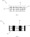
FIG. 1 is a schematic view of a tape of an embodiment of the present disclosure; -
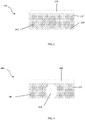
FIG. 2 is a schematic view of a tape of another embodiment of the present disclosure; -
FIG. 3 is a schematic view of a tape having suction cup morphology of another embodiment of the present disclosure; -
FIG. 4 is a schematic view of a tape of another embodiment of the present disclosure; -
FIG. 5 is a schematic view of a tape of another embodiment of the present disclosure; -
FIG. 6 is a schematic view of a tape of another embodiment of the present disclosure; and -
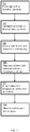
FIG. 7 is a diagram showing use of thermal managing electrical connection tape. - This invention is not limited in its application to the details of construction and the arrangement of components set forth in the following description or illustrated in the drawings. The invention is capable of embodiments and of being practiced or of being carried out in various ways beyond those exemplarily presented herein.
- Thermal managing electrical connection tape of embodiments of the present disclosure is designed to take advantage of a metal's affinity for other metals. A thermal managing electrical connection tape of embodiments of the present disclosure includes a resilient film having a flux composition, including soldering flux and a solder powder, applied to the film. The tape is laminated (or pressed in place) between two substrates containing metallization to be connected. In certain embodiments, the substrates can be fabricated from any suitable metal, such as copper, silver, tin, gold, etc. The thermal managing electrical connection tape, sometimes referred to as "TMECT," is then heated in accordance with a temperature profile that reaches a melt temperature of the particular metal or alloy used in the substrate. In certain embodiments, the temperatures and the times are dependent on the metal or alloy used, the film thickness and the type of substrate. For example, the temperature to be applied can be 10-20 °C above the melting temperature of the metal or alloy, and the duration can be between 20-30 seconds. As the temperature rises, the tape having the resilient carrier film and the soldering flux/solder powder composition melts. Once bulk melting has begun, the flux both deoxidizes and acts as a transport mechanism for the solder. When the solder alloy melt temperature is reached, the deoxidized solder wets only the substrate metallization, and the stranded solder is transported by the liquid flux to the desired metallization areas. After the solder has been transported to the metallization, the entire sample is allowed to cool. The final product is two substrates electrically connected on the metalized areas only, and contains completely electrically isolated connections.
- Referring to
FIG. 1 , a thermal managing electrical connection tape is generally indicated at 100, and includes aresilient film 120 having asoldering flux composition 110 applied to the film. As shown, theflux composition 110 includes a soldering flux and asolder powder 140 incorporated or embedded within the soldering flux. In some embodiments, thefilm 120 may include a carrier film suitable for material applications. Theflux composition 110 may include a solvent, polymer, an activator, a rosin or resin, a corrosion inhibitor, or combinations of these constituents. In some embodiments, the solvent may be methylcyclohexane or ethanol. In some embodiments, the polymer may be Versamid® 940 or Polyvinylpyrrolidone (PVP). In some embodiments, the activator may be a dicarboxylic acid such as adipic acid or may be dibromobutendiol, or iodobenzoic acid, or cyclohexylamine HCl. In some embodiments, the resin may be, for example, Dymerex. In some embodiments, the corrosion inhibitor may be, for example, benzotriazole. - The
solder powder 140 is compatible with the soldering flux of theflux composition 110. In some embodiments,solder powder 140 may include a lead-free solder. In some embodiments,solder powder 140 may include a mixture of tin, silver, and copper. For example,solder powder 140 may include SAC305 solder alloy.Solder powder 140 may include particles of any size compatible with the application. For example,solder powder 140 may include Type 3 particle sizes of 25 µm to 45 µm. Any suitable solder compatible with theflux composition 110 can be provided. - The
flux composition 110 and thesolder powder 140 may be in any mixture composition. The composition may vary depending on the end application. In the invention theflux composition 110 includes about 30 wt % to about 50 wt% solder powder 140 and about 50 wt % to about 70 wt % soldering flux. For example, theflux composition 110 may include a slurry containing about 40 wt% solder powder 140 and about 60 wt % soldering flux. The slurry may be cast on thefilm 120, dried in a drying furnace and slit to the desired film width to create a TMECT. For example, the drying temperature may be approximately 10-15 °C below a boiling point of the solvent for approximately 5-15 minutes, depending on the cast thickness. - Referring to
FIG. 2 , a TMECT, generally indicated at 200, can also be patterned with epoxy and/oracrylic 250, which is interspersed within theflux composition 110. The patterned epoxy and/oracrylic TMECT 200 is designed to add strength and the ability to increase a bond line of a processed substrate. The epoxy and/oracrylic TMECT 250 may also limit solder shorting potential. - Referring to
FIG. 3 , a TMECT, generally indicated at 300, can be processed to construct "suction cup" morphology, indicated at 350, which is formed on a bottom of the tape. Thesuction cup morphology 350 can eliminate a typical lamination step required for anisotropic conductive films by making thetape 300 able to be initially pressed and fixed to its desired substrate without added heat. - Referring to
FIG. 4 , a TMECT, generally indicated at 400, contains filler materials, the filler beingglass frit 450, to make the process more reliable at higher pressures. - Referring to
FIG. 5 , a TMECT, generally indicated at 500, may also containadditives 550, such as Leuco, Leuco-like, or liquid crystal "thermochromic" dyes for process temperature and residue evaluations. - The
tapes FIGS. 1-5 , respectively, contrast with anisotropic conductive paste (ACF), an example of which is shown inFIG. 6 . As shown, a tape generally indicated at 600 includes acarrier film 620 and a paste 610 (epoxy and/or acrylic) applied to the film. In one embodiment thepaste 610 includesconductive particles 630 embedded in the paste. A typical ACF includes a conducting particle, for example, a polymer plated with layers of Ni/Au, in an epoxy and/or acrylic matrix. ACF can be laminated in place by curing the epoxy and/or acrylic, which essentially glues the film to the substrate. Electrical connections between metalized substrates are then made by applying between 1-100 mPa of pressure (film and substrate dependent) to the substrates, thus crushing the conductive particles between the metallization and creating a low current carrying capacity connection. - In some embodiments, the thermal managing electrical connection tape of embodiments of the present disclosure can be most closely related to the ACF platform, but can be used as a replacement for any of the above-identified compositions and processes. The TMECT is highly reliable in connecting fine pitched features, does not require pressure, can be directly attached to the substrate without use of paste, offers a low resistance connection, does not need to be refrigerated, inexpensive to manufacture and in some instance can eliminate a classic ACF lamination and standard perform placement process step. The TMECT can also easily be adapted for standard die attach processes such as Die transfer film (DTF) and wafer backside (WBS) processing.
-
FIG. 7 is a process diagram illustrating a method of using thermal managing electrical connection film as an ACF replacement. Thefirst step 701 includes placing the film on a first metalized substrate. Next, the film is laminated or pressed onto the first metalized substrate (step 702). The sample is allowed to cool and the laminate backing is removed instep 703. After cooling, the second metalized substrate is aligned with the first metalized substrate (step 704) to form an assembly. The assembly is then brought to the alloy melt temperature and held for about 90 seconds (step 705). Finally, the assembly is allowed to cool to room temperature (step 706). - In a certain embodiment, a method of fabricating an assembly comprising a thermal managing electrical connection tape includes laminating a tape between two substrates containing metallization to be connected, with the tape including a resilient carrier film and a composition having soldering flux and solder powder applied to the carrier film. The laminated tape and substrates is heated to a melting temperature of the solder powder. As the temperature rises, the carrier film melts on which the composition is applied. Once bulk melting of the carrier film has begun, the soldering flux deoxidizes and acts as a transport mechanism for the solder powder. When the melting temperature is reached, the deoxidized solder wets only the substrate metallization, and stranded solder powder is transported by a liquid flux to a desired metallization area. Finally, the tape is cooled. Embodiments of the method include laminating of the tape between the two substrates at a temperature 90-187 °C and a pressure 0.14 to 227 kPa (0.02-33 psi) for 1-10 seconds. Melting temperature of the solder powder is between 137-289 °C.
- A thermal managing electrical connection tape including a carrier film and a flux composition having soldering flux and solder powder was prepared. The tape was prepared by adding 15.5 wt % methylcyclohexane to a glass or stainless steel container with mixing capability. About 46.6 wt % ethanol was added to the solution and mixed until homogeneous. Next, about 15.6 wt % of Versamid® 940 was added to the solution, and mixed until the solution was clear. Approximately 9.6 wt % of Dymerex was then added to the solution and again mixed until the solution was clear. Then, about 0.2 wt % iodobenzoic acid was added to the solution and mixed until the solution was clear. About 1.4 wt % of dibromobutendiol was then added to the solution and mixed until the solution was clear. Next, about 0.2 wt % cyclohexylamine HCl was added to the solution and mixed until the solution was clear. About 10.8 wt % adipic acid was then added to the solution and mixed until the solution was clear. Finally, about 0.1 wt % benzotriazole was added to the solution and mixed until the solution was clear.
- A solder powder, SAC305 Type 3, was then added to the soldering flux solution to create a slurry comprising about 40 wt % solder powder and 60 wt % flux film. The composition may vary depending on the end application. The slurry was cast with a carrier film into a tape, dried in a drying furnace, and slit to the desired tape width. Depending on the cast thickness, the drying temperature is approximately 10-15 °C below a boiling point of the solvent for approximately 5-15 minutes.
Claims (10)
- A thermal managing electrical connection tape comprising:a carrier film; anda composition including solder powder and soldering flux;wherein the composition contains between 50 wt % and 70 wt % soldering flux and between 30 wt % and 50 wt % solder powder, the composition being applied to the carrier film, characterized in that the composition includes glass frit.
- The thermal managing electrical connection tape of claim 1, wherein the solder powder is disposed in the soldering flux.
- The thermal managing electrical connection tape of claim 1 or claim 2, wherein the composition includes at least one of epoxy and acrylic.
- The thermal managing electrical connection tape of claim 1, wherein the composition is configured to have a suction cup morphology (350) formed on the bottom of the tape.
- The thermal managing electrical connection tape of claim 1, wherein the composition further includes liquid crystal thermochromic dyes.
- A method of fabricating a thermal managing electrical connection tape, the method comprising:providing a composition including a soldering flux and optionally epoxy and/or acrylic;adding a solder powder to the composition, wherein the composition contains between 50 wt % and 70 wt % soldering flux and between 30 wt % and 50 wt % solder powder;casting the composition on a carrier film;drying the carrier film in a drying furnace to form a dried tape; andcutting the dried tape to a desired width to form a thermal managing electrical connection tape, the method characterized in that the composition includes glass fritt.
- The method of claim 6, wherein drying the tape in a drying furnace includes drying the tape at 10-15 °C below a boiling point of a solvent of the composition for 5-15 minutes.
- A method of fabricating an assembly comprising a thermal managing electrical connection tape, the method comprising:laminating a tape between two substrates containing metallization to be connected, the tape including a resilient carrier film and a composition having soldering flux and solder powder applied to the carrier film, wherein the composition contains between 50 wt % and 70 wt % soldering flux and between 30 wt % and 50 wt % solder powder;heating the laminated tape and substrates to a melting temperature of the solder powder;as the temperature raises, melting the carrier film on which the composition is applied;once bulk melting of the carrier film has begun, the soldering flux deoxidizes and acts as a transport mechanism for the solder powder;when the melting temperature is reached, the deoxidized solder wets only the substrate metallization, and stranded solder powder is transported by a liquid flux to a desired metallization area; andcooling the tape, the method characterized in that the composition includes glass fritt.
- The method of claim 8, wherein the laminating of the tape between the two substrates is achieved at a temperature 90-187°C and a pressure 0.14 to 227 kPa (0.02-33 psi) for 1-10 seconds.
- The method of claim 8, wherein the melting temperature of the solder powder is between 137-289 °C.
Priority Applications (1)
| Application Number | Priority Date | Filing Date | Title |
|---|---|---|---|
| EP22162649.2A EP4037103A1 (en) | 2015-02-11 | 2016-02-10 | Electrical connection tape |
Applications Claiming Priority (2)
| Application Number | Priority Date | Filing Date | Title |
|---|---|---|---|
| US201562114820P | 2015-02-11 | 2015-02-11 | |
| PCT/US2016/017331 WO2016130662A1 (en) | 2015-02-11 | 2016-02-10 | Electrical connection tape |
Related Child Applications (2)
| Application Number | Title | Priority Date | Filing Date |
|---|---|---|---|
| EP22162649.2A Division-Into EP4037103A1 (en) | 2015-02-11 | 2016-02-10 | Electrical connection tape |
| EP22162649.2A Division EP4037103A1 (en) | 2015-02-11 | 2016-02-10 | Electrical connection tape |
Publications (3)
| Publication Number | Publication Date |
|---|---|
| EP3257109A1 EP3257109A1 (en) | 2017-12-20 |
| EP3257109A4 EP3257109A4 (en) | 2018-08-01 |
| EP3257109B1 true EP3257109B1 (en) | 2022-06-22 |
Family
ID=56614813
Family Applications (2)
| Application Number | Title | Priority Date | Filing Date |
|---|---|---|---|
| EP22162649.2A Pending EP4037103A1 (en) | 2015-02-11 | 2016-02-10 | Electrical connection tape |
| EP16749792.4A Active EP3257109B1 (en) | 2015-02-11 | 2016-02-10 | Electrical connection tape |
Family Applications Before (1)
| Application Number | Title | Priority Date | Filing Date |
|---|---|---|---|
| EP22162649.2A Pending EP4037103A1 (en) | 2015-02-11 | 2016-02-10 | Electrical connection tape |
Country Status (6)
| Country | Link |
|---|---|
| US (1) | US10625356B2 (en) |
| EP (2) | EP4037103A1 (en) |
| JP (1) | JP6995621B2 (en) |
| KR (1) | KR102038377B1 (en) |
| TW (1) | TWI772254B (en) |
| WO (1) | WO2016130662A1 (en) |
Families Citing this family (1)
| Publication number | Priority date | Publication date | Assignee | Title |
|---|---|---|---|---|
| US10160066B2 (en) * | 2016-11-01 | 2018-12-25 | GM Global Technology Operations LLC | Methods and systems for reinforced adhesive bonding using solder elements and flux |
Family Cites Families (25)
| Publication number | Priority date | Publication date | Assignee | Title |
|---|---|---|---|---|
| US4667869A (en) | 1981-10-05 | 1987-05-26 | Raychem Corporation | Soldering methods and devices |
| JPH0247459B2 (en) | 1982-07-28 | 1990-10-19 | Dainippon Ink & Chemicals | SHINKINEMACHITSUKUEKISHOKAGOBUTSU |
| JPS5921650U (en) * | 1982-07-28 | 1984-02-09 | 岩崎電気株式会社 | double-sided adhesive |
| JPS61276873A (en) | 1985-05-31 | 1986-12-06 | Sony Chem Kk | Electrically conductive anisotropic adhesive |
| JP3134703B2 (en) | 1995-03-07 | 2001-02-13 | 松下電器産業株式会社 | Apparatus and method for applying flux for soldering electronic components |
| DE69636971T2 (en) * | 1995-05-24 | 2007-12-13 | Fry's Metals Inc. | SOFT LOT FLUX ON EPOXY BASE WITHOUT VOLATILE ORGANIC COMPOUNDS |
| DE69710089T2 (en) * | 1996-08-16 | 2002-08-22 | Hugh P. Craig | PRINTABLE COMPOSITIONS AND THEIR APPLICATION ON DIELECTRIC SURFACES FOR THE PRODUCTION OF PRINTED CIRCUITS |
| US7022266B1 (en) * | 1996-08-16 | 2006-04-04 | Dow Corning Corporation | Printable compositions, and their application to dielectric surfaces used in the manufacture of printed circuit boards |
| US6337522B1 (en) * | 1997-07-10 | 2002-01-08 | International Business Machines Corporation | Structure employing electrically conductive adhesives |
| JP2001164210A (en) | 1999-12-13 | 2001-06-19 | Sumitomo Bakelite Co Ltd | Anisotropic conductive film and electronic equipment using the same |
| US7182241B2 (en) * | 2002-08-09 | 2007-02-27 | Micron Technology, Inc. | Multi-functional solder and articles made therewith, such as microelectronic components |
| US7303698B2 (en) | 2003-11-19 | 2007-12-04 | E.I. Du Pont De Nemours And Company | Thick film conductor case compositions for LTCC tape |
| JP4715847B2 (en) * | 2006-04-24 | 2011-07-06 | 日立化成工業株式会社 | Adhesive tape |
| JPWO2007125650A1 (en) | 2006-04-27 | 2009-09-10 | 住友ベークライト株式会社 | Adhesive tape, semiconductor package and electronic equipment |
| US7754005B2 (en) * | 2006-05-02 | 2010-07-13 | Kyphon Sarl | Bone cement compositions comprising an indicator agent and related methods thereof |
| EP2055756A1 (en) * | 2006-08-25 | 2009-05-06 | Sumitomo Bakelite Company, Ltd. | Adhesive tape, joint structure, and semiconductor package |
| TWI414580B (en) * | 2006-10-31 | 2013-11-11 | 住友電木股份有限公司 | Adhesive tape and semiconductor device using the same |
| JP5277564B2 (en) | 2007-05-29 | 2013-08-28 | 住友ベークライト株式会社 | Semiconductor wafer bonding method and semiconductor device manufacturing method |
| US7911059B2 (en) * | 2007-06-08 | 2011-03-22 | SeniLEDS Optoelectronics Co., Ltd | High thermal conductivity substrate for a semiconductor device |
| EP2357876A4 (en) | 2008-09-05 | 2012-04-25 | Sumitomo Bakelite Co | ELECTROCONDUCTIVE CONNECTION MATERIAL, METHOD FOR CONNECTING TERMINALS TO OTHER BY USING THE ELECTROCONDUCTIVE CONNECTION MATERIAL, AND METHOD FOR MANUFACTURING CONNECTION TERMINAL |
| JP4959778B2 (en) | 2009-12-10 | 2012-06-27 | 信越化学工業株式会社 | Photocurable resin composition, film adhesive using the composition, and adhesive sheet |
| JP5728636B2 (en) * | 2010-09-29 | 2015-06-03 | パナソニックIpマネジメント株式会社 | Conductive adhesive, circuit board using the same, and electronic component module |
| WO2012063386A1 (en) | 2010-11-08 | 2012-05-18 | パナソニック株式会社 | Production method for solder transfer base material, solder precoating method, and solder transfer base material |
| TWI612591B (en) | 2011-10-26 | 2018-01-21 | 日立化成股份有限公司 | Reflow film, solder bump forming method, solder bonding forming method, and semiconductor device |
| JP2015009394A (en) * | 2013-06-27 | 2015-01-19 | 京セラ株式会社 | Piezoelectric actuator and liquid discharge head and recording device using piezoelectric actuator |
-
2016
- 2016-02-10 US US15/549,535 patent/US10625356B2/en active Active
- 2016-02-10 WO PCT/US2016/017331 patent/WO2016130662A1/en not_active Ceased
- 2016-02-10 EP EP22162649.2A patent/EP4037103A1/en active Pending
- 2016-02-10 KR KR1020177025406A patent/KR102038377B1/en active Active
- 2016-02-10 EP EP16749792.4A patent/EP3257109B1/en active Active
- 2016-02-10 JP JP2017542083A patent/JP6995621B2/en active Active
- 2016-02-15 TW TW105104335A patent/TWI772254B/en active
Also Published As
| Publication number | Publication date |
|---|---|
| US20180036818A1 (en) | 2018-02-08 |
| TW201635314A (en) | 2016-10-01 |
| JP6995621B2 (en) | 2022-01-14 |
| US10625356B2 (en) | 2020-04-21 |
| WO2016130662A1 (en) | 2016-08-18 |
| EP3257109A4 (en) | 2018-08-01 |
| EP3257109A1 (en) | 2017-12-20 |
| KR102038377B1 (en) | 2019-10-31 |
| KR20170118783A (en) | 2017-10-25 |
| TWI772254B (en) | 2022-08-01 |
| JP2018505060A (en) | 2018-02-22 |
| EP4037103A1 (en) | 2022-08-03 |
Similar Documents
| Publication | Publication Date | Title |
|---|---|---|
| US5328087A (en) | Thermally and electrically conductive adhesive material and method of bonding with same | |
| CN102482540B (en) | Anisotropic conductive adhesive for ultrasonic bonding, and electronic component connection method using same | |
| CN101432095B (en) | Solder Foam and Electronics | |
| US5445308A (en) | Thermally conductive connection with matrix material and randomly dispersed filler containing liquid metal | |
| CN103106951B (en) | Anisotropic conductive material | |
| CN101641176B (en) | High temperature welding material | |
| CN100594089C (en) | Solder composition, connecting process and substrate producing process using soldering | |
| US6646355B2 (en) | Structure comprising beam leads bonded with electrically conductive adhesive | |
| TW201124542A (en) | Preparation of metallurgic network compositions and methods of use thereof | |
| WO2003097294A1 (en) | Solder compositions for attaching a die to a substrate | |
| CN104245204A (en) | Bonding method, bond structure, and manufacturing method for same | |
| CN1947480B (en) | How to install electronic components | |
| JP2008238233A (en) | Lead-free alloy joining material, joining method and joined body | |
| JP5077684B2 (en) | Au-Sn alloy solder paste for pin transfer | |
| JP2011251330A (en) | High-temperature lead-free solder paste | |
| US10625356B2 (en) | Electrical connection tape | |
| JP6335588B2 (en) | Method for producing anisotropic conductive adhesive | |
| CN112961633A (en) | Low-temperature cured conductive adhesive and preparation method thereof | |
| KR100777255B1 (en) | Anisotropic conductive film and mounting method of electronic component using same | |
| JP5113390B2 (en) | Wiring connection method | |
| JP2007081198A (en) | Conductive connection method between terminals | |
| JP2023176346A (en) | Manufacturing method of circuit connection structure and circuit connection device | |
| WO2019146587A1 (en) | Joining layer of semiconductor module, semiconductor module, and method for manufacturing same | |
| JP2007260695A (en) | Bonding material, bonding method, and bonded body | |
| CN107405729A (en) | Soldering paste |
Legal Events
| Date | Code | Title | Description |
|---|---|---|---|
| STAA | Information on the status of an ep patent application or granted ep patent |
Free format text: STATUS: THE INTERNATIONAL PUBLICATION HAS BEEN MADE |
|
| PUAI | Public reference made under article 153(3) epc to a published international application that has entered the european phase |
Free format text: ORIGINAL CODE: 0009012 |
|
| STAA | Information on the status of an ep patent application or granted ep patent |
Free format text: STATUS: REQUEST FOR EXAMINATION WAS MADE |
|
| 17P | Request for examination filed |
Effective date: 20170911 |
|
| AK | Designated contracting states |
Kind code of ref document: A1 Designated state(s): AL AT BE BG CH CY CZ DE DK EE ES FI FR GB GR HR HU IE IS IT LI LT LU LV MC MK MT NL NO PL PT RO RS SE SI SK SM TR |
|
| AX | Request for extension of the european patent |
Extension state: BA ME |
|
| DAV | Request for validation of the european patent (deleted) | ||
| DAX | Request for extension of the european patent (deleted) | ||
| A4 | Supplementary search report drawn up and despatched |
Effective date: 20180703 |
|
| RIC1 | Information provided on ipc code assigned before grant |
Ipc: B23K 35/362 20060101ALI20180627BHEP Ipc: B23K 101/36 20060101ALN20180627BHEP Ipc: B23K 35/36 20060101ALI20180627BHEP Ipc: B23K 35/02 20060101ALI20180627BHEP Ipc: B23K 35/26 20060101ALI20180627BHEP Ipc: H01R 4/04 20060101AFI20180627BHEP Ipc: B23K 35/00 20060101ALI20180627BHEP |
|
| STAA | Information on the status of an ep patent application or granted ep patent |
Free format text: STATUS: EXAMINATION IS IN PROGRESS |
|
| 17Q | First examination report despatched |
Effective date: 20191211 |
|
| REG | Reference to a national code |
Ref country code: DE Ref legal event code: R079 Ref document number: 602016072998 Country of ref document: DE Free format text: PREVIOUS MAIN CLASS: H01R0004000000 Ipc: H01R0004040000 |
|
| GRAP | Despatch of communication of intention to grant a patent |
Free format text: ORIGINAL CODE: EPIDOSNIGR1 |
|
| STAA | Information on the status of an ep patent application or granted ep patent |
Free format text: STATUS: GRANT OF PATENT IS INTENDED |
|
| RIC1 | Information provided on ipc code assigned before grant |
Ipc: B23K 101/42 20060101ALN20211217BHEP Ipc: B23K 101/36 20060101ALN20211217BHEP Ipc: C09J 7/10 20180101ALI20211217BHEP Ipc: B23K 1/20 20060101ALI20211217BHEP Ipc: B23K 1/00 20060101ALI20211217BHEP Ipc: B23K 3/04 20060101ALI20211217BHEP Ipc: B23K 35/362 20060101ALI20211217BHEP Ipc: B23K 35/36 20060101ALI20211217BHEP Ipc: B23K 35/26 20060101ALI20211217BHEP Ipc: B23K 35/02 20060101ALI20211217BHEP Ipc: B23K 35/00 20060101ALI20211217BHEP Ipc: H01R 4/04 20060101AFI20211217BHEP |
|
| INTG | Intention to grant announced |
Effective date: 20220126 |
|
| GRAS | Grant fee paid |
Free format text: ORIGINAL CODE: EPIDOSNIGR3 |
|
| GRAA | (expected) grant |
Free format text: ORIGINAL CODE: 0009210 |
|
| STAA | Information on the status of an ep patent application or granted ep patent |
Free format text: STATUS: THE PATENT HAS BEEN GRANTED |
|
| AK | Designated contracting states |
Kind code of ref document: B1 Designated state(s): AL AT BE BG CH CY CZ DE DK EE ES FI FR GB GR HR HU IE IS IT LI LT LU LV MC MK MT NL NO PL PT RO RS SE SI SK SM TR |
|
| REG | Reference to a national code |
Ref country code: GB Ref legal event code: FG4D |
|
| REG | Reference to a national code |
Ref country code: CH Ref legal event code: EP |
|
| REG | Reference to a national code |
Ref country code: DE Ref legal event code: R096 Ref document number: 602016072998 Country of ref document: DE |
|
| REG | Reference to a national code |
Ref country code: AT Ref legal event code: REF Ref document number: 1500392 Country of ref document: AT Kind code of ref document: T Effective date: 20220715 |
|
| REG | Reference to a national code |
Ref country code: IE Ref legal event code: FG4D |
|
| REG | Reference to a national code |
Ref country code: NL Ref legal event code: FP |
|
| REG | Reference to a national code |
Ref country code: LT Ref legal event code: MG9D |
|
| PG25 | Lapsed in a contracting state [announced via postgrant information from national office to epo] |
Ref country code: SE Free format text: LAPSE BECAUSE OF FAILURE TO SUBMIT A TRANSLATION OF THE DESCRIPTION OR TO PAY THE FEE WITHIN THE PRESCRIBED TIME-LIMIT Effective date: 20220622 Ref country code: NO Free format text: LAPSE BECAUSE OF FAILURE TO SUBMIT A TRANSLATION OF THE DESCRIPTION OR TO PAY THE FEE WITHIN THE PRESCRIBED TIME-LIMIT Effective date: 20220922 Ref country code: LT Free format text: LAPSE BECAUSE OF FAILURE TO SUBMIT A TRANSLATION OF THE DESCRIPTION OR TO PAY THE FEE WITHIN THE PRESCRIBED TIME-LIMIT Effective date: 20220622 Ref country code: HR Free format text: LAPSE BECAUSE OF FAILURE TO SUBMIT A TRANSLATION OF THE DESCRIPTION OR TO PAY THE FEE WITHIN THE PRESCRIBED TIME-LIMIT Effective date: 20220622 Ref country code: GR Free format text: LAPSE BECAUSE OF FAILURE TO SUBMIT A TRANSLATION OF THE DESCRIPTION OR TO PAY THE FEE WITHIN THE PRESCRIBED TIME-LIMIT Effective date: 20220923 Ref country code: FI Free format text: LAPSE BECAUSE OF FAILURE TO SUBMIT A TRANSLATION OF THE DESCRIPTION OR TO PAY THE FEE WITHIN THE PRESCRIBED TIME-LIMIT Effective date: 20220622 Ref country code: BG Free format text: LAPSE BECAUSE OF FAILURE TO SUBMIT A TRANSLATION OF THE DESCRIPTION OR TO PAY THE FEE WITHIN THE PRESCRIBED TIME-LIMIT Effective date: 20220922 |
|
| REG | Reference to a national code |
Ref country code: AT Ref legal event code: MK05 Ref document number: 1500392 Country of ref document: AT Kind code of ref document: T Effective date: 20220622 |
|
| PG25 | Lapsed in a contracting state [announced via postgrant information from national office to epo] |
Ref country code: RS Free format text: LAPSE BECAUSE OF FAILURE TO SUBMIT A TRANSLATION OF THE DESCRIPTION OR TO PAY THE FEE WITHIN THE PRESCRIBED TIME-LIMIT Effective date: 20220622 Ref country code: LV Free format text: LAPSE BECAUSE OF FAILURE TO SUBMIT A TRANSLATION OF THE DESCRIPTION OR TO PAY THE FEE WITHIN THE PRESCRIBED TIME-LIMIT Effective date: 20220622 |
|
| PG25 | Lapsed in a contracting state [announced via postgrant information from national office to epo] |
Ref country code: SM Free format text: LAPSE BECAUSE OF FAILURE TO SUBMIT A TRANSLATION OF THE DESCRIPTION OR TO PAY THE FEE WITHIN THE PRESCRIBED TIME-LIMIT Effective date: 20220622 Ref country code: SK Free format text: LAPSE BECAUSE OF FAILURE TO SUBMIT A TRANSLATION OF THE DESCRIPTION OR TO PAY THE FEE WITHIN THE PRESCRIBED TIME-LIMIT Effective date: 20220622 Ref country code: RO Free format text: LAPSE BECAUSE OF FAILURE TO SUBMIT A TRANSLATION OF THE DESCRIPTION OR TO PAY THE FEE WITHIN THE PRESCRIBED TIME-LIMIT Effective date: 20220622 Ref country code: PT Free format text: LAPSE BECAUSE OF FAILURE TO SUBMIT A TRANSLATION OF THE DESCRIPTION OR TO PAY THE FEE WITHIN THE PRESCRIBED TIME-LIMIT Effective date: 20221024 Ref country code: ES Free format text: LAPSE BECAUSE OF FAILURE TO SUBMIT A TRANSLATION OF THE DESCRIPTION OR TO PAY THE FEE WITHIN THE PRESCRIBED TIME-LIMIT Effective date: 20220622 Ref country code: EE Free format text: LAPSE BECAUSE OF FAILURE TO SUBMIT A TRANSLATION OF THE DESCRIPTION OR TO PAY THE FEE WITHIN THE PRESCRIBED TIME-LIMIT Effective date: 20220622 Ref country code: CZ Free format text: LAPSE BECAUSE OF FAILURE TO SUBMIT A TRANSLATION OF THE DESCRIPTION OR TO PAY THE FEE WITHIN THE PRESCRIBED TIME-LIMIT Effective date: 20220622 Ref country code: AT Free format text: LAPSE BECAUSE OF FAILURE TO SUBMIT A TRANSLATION OF THE DESCRIPTION OR TO PAY THE FEE WITHIN THE PRESCRIBED TIME-LIMIT Effective date: 20220622 |
|
| PG25 | Lapsed in a contracting state [announced via postgrant information from national office to epo] |
Ref country code: PL Free format text: LAPSE BECAUSE OF FAILURE TO SUBMIT A TRANSLATION OF THE DESCRIPTION OR TO PAY THE FEE WITHIN THE PRESCRIBED TIME-LIMIT Effective date: 20220622 Ref country code: IS Free format text: LAPSE BECAUSE OF FAILURE TO SUBMIT A TRANSLATION OF THE DESCRIPTION OR TO PAY THE FEE WITHIN THE PRESCRIBED TIME-LIMIT Effective date: 20221022 |
|
| REG | Reference to a national code |
Ref country code: DE Ref legal event code: R097 Ref document number: 602016072998 Country of ref document: DE |
|
| PG25 | Lapsed in a contracting state [announced via postgrant information from national office to epo] |
Ref country code: AL Free format text: LAPSE BECAUSE OF FAILURE TO SUBMIT A TRANSLATION OF THE DESCRIPTION OR TO PAY THE FEE WITHIN THE PRESCRIBED TIME-LIMIT Effective date: 20220622 |
|
| PG25 | Lapsed in a contracting state [announced via postgrant information from national office to epo] |
Ref country code: DK Free format text: LAPSE BECAUSE OF FAILURE TO SUBMIT A TRANSLATION OF THE DESCRIPTION OR TO PAY THE FEE WITHIN THE PRESCRIBED TIME-LIMIT Effective date: 20220622 |
|
| PLBE | No opposition filed within time limit |
Free format text: ORIGINAL CODE: 0009261 |
|
| STAA | Information on the status of an ep patent application or granted ep patent |
Free format text: STATUS: NO OPPOSITION FILED WITHIN TIME LIMIT |
|
| 26N | No opposition filed |
Effective date: 20230323 |
|
| P01 | Opt-out of the competence of the unified patent court (upc) registered |
Effective date: 20230524 |
|
| PG25 | Lapsed in a contracting state [announced via postgrant information from national office to epo] |
Ref country code: SI Free format text: LAPSE BECAUSE OF FAILURE TO SUBMIT A TRANSLATION OF THE DESCRIPTION OR TO PAY THE FEE WITHIN THE PRESCRIBED TIME-LIMIT Effective date: 20220622 |
|
| PG25 | Lapsed in a contracting state [announced via postgrant information from national office to epo] |
Ref country code: MC Free format text: LAPSE BECAUSE OF FAILURE TO SUBMIT A TRANSLATION OF THE DESCRIPTION OR TO PAY THE FEE WITHIN THE PRESCRIBED TIME-LIMIT Effective date: 20220622 |
|
| REG | Reference to a national code |
Ref country code: CH Ref legal event code: PL |
|
| REG | Reference to a national code |
Ref country code: BE Ref legal event code: MM Effective date: 20230228 |
|
| PG25 | Lapsed in a contracting state [announced via postgrant information from national office to epo] |
Ref country code: LU Free format text: LAPSE BECAUSE OF NON-PAYMENT OF DUE FEES Effective date: 20230210 Ref country code: LI Free format text: LAPSE BECAUSE OF NON-PAYMENT OF DUE FEES Effective date: 20230228 Ref country code: CH Free format text: LAPSE BECAUSE OF NON-PAYMENT OF DUE FEES Effective date: 20230228 |
|
| REG | Reference to a national code |
Ref country code: IE Ref legal event code: MM4A |
|
| PG25 | Lapsed in a contracting state [announced via postgrant information from national office to epo] |
Ref country code: IT Free format text: LAPSE BECAUSE OF FAILURE TO SUBMIT A TRANSLATION OF THE DESCRIPTION OR TO PAY THE FEE WITHIN THE PRESCRIBED TIME-LIMIT Effective date: 20220622 Ref country code: IE Free format text: LAPSE BECAUSE OF NON-PAYMENT OF DUE FEES Effective date: 20230210 |
|
| PG25 | Lapsed in a contracting state [announced via postgrant information from national office to epo] |
Ref country code: BE Free format text: LAPSE BECAUSE OF NON-PAYMENT OF DUE FEES Effective date: 20230228 |
|
| PG25 | Lapsed in a contracting state [announced via postgrant information from national office to epo] |
Ref country code: BG Free format text: LAPSE BECAUSE OF FAILURE TO SUBMIT A TRANSLATION OF THE DESCRIPTION OR TO PAY THE FEE WITHIN THE PRESCRIBED TIME-LIMIT Effective date: 20220622 |
|
| PG25 | Lapsed in a contracting state [announced via postgrant information from national office to epo] |
Ref country code: BG Free format text: LAPSE BECAUSE OF FAILURE TO SUBMIT A TRANSLATION OF THE DESCRIPTION OR TO PAY THE FEE WITHIN THE PRESCRIBED TIME-LIMIT Effective date: 20220622 |
|
| PG25 | Lapsed in a contracting state [announced via postgrant information from national office to epo] |
Ref country code: CY Free format text: LAPSE BECAUSE OF FAILURE TO SUBMIT A TRANSLATION OF THE DESCRIPTION OR TO PAY THE FEE WITHIN THE PRESCRIBED TIME-LIMIT; INVALID AB INITIO Effective date: 20160210 |
|
| PG25 | Lapsed in a contracting state [announced via postgrant information from national office to epo] |
Ref country code: HU Free format text: LAPSE BECAUSE OF FAILURE TO SUBMIT A TRANSLATION OF THE DESCRIPTION OR TO PAY THE FEE WITHIN THE PRESCRIBED TIME-LIMIT; INVALID AB INITIO Effective date: 20160210 |
|
| PG25 | Lapsed in a contracting state [announced via postgrant information from national office to epo] |
Ref country code: TR Free format text: LAPSE BECAUSE OF FAILURE TO SUBMIT A TRANSLATION OF THE DESCRIPTION OR TO PAY THE FEE WITHIN THE PRESCRIBED TIME-LIMIT Effective date: 20220622 |
|
| PGFP | Annual fee paid to national office [announced via postgrant information from national office to epo] |
Ref country code: NL Payment date: 20260121 Year of fee payment: 11 |
|
| PGFP | Annual fee paid to national office [announced via postgrant information from national office to epo] |
Ref country code: GB Payment date: 20260121 Year of fee payment: 11 |
|
| PGFP | Annual fee paid to national office [announced via postgrant information from national office to epo] |
Ref country code: DE Payment date: 20260121 Year of fee payment: 11 |
|
| PGFP | Annual fee paid to national office [announced via postgrant information from national office to epo] |
Ref country code: FR Payment date: 20260121 Year of fee payment: 11 |