EP3254307B1 - Radially outward pad design for electrostatic chuck surface - Google Patents
Radially outward pad design for electrostatic chuck surface Download PDFInfo
- Publication number
- EP3254307B1 EP3254307B1 EP16746928.7A EP16746928A EP3254307B1 EP 3254307 B1 EP3254307 B1 EP 3254307B1 EP 16746928 A EP16746928 A EP 16746928A EP 3254307 B1 EP3254307 B1 EP 3254307B1
- Authority
- EP
- European Patent Office
- Prior art keywords
- electrostatic chuck
- chuck assembly
- elongated features
- gas
- substrate
- Prior art date
- Legal status (The legal status is an assumption and is not a legal conclusion. Google has not performed a legal analysis and makes no representation as to the accuracy of the status listed.)
- Active
Links
Images

Classifications
-
- C—CHEMISTRY; METALLURGY
- C23—COATING METALLIC MATERIAL; COATING MATERIAL WITH METALLIC MATERIAL; CHEMICAL SURFACE TREATMENT; DIFFUSION TREATMENT OF METALLIC MATERIAL; COATING BY VACUUM EVAPORATION, BY SPUTTERING, BY ION IMPLANTATION OR BY CHEMICAL VAPOUR DEPOSITION, IN GENERAL; INHIBITING CORROSION OF METALLIC MATERIAL OR INCRUSTATION IN GENERAL
- C23C—COATING METALLIC MATERIAL; COATING MATERIAL WITH METALLIC MATERIAL; SURFACE TREATMENT OF METALLIC MATERIAL BY DIFFUSION INTO THE SURFACE, BY CHEMICAL CONVERSION OR SUBSTITUTION; COATING BY VACUUM EVAPORATION, BY SPUTTERING, BY ION IMPLANTATION OR BY CHEMICAL VAPOUR DEPOSITION, IN GENERAL
- C23C14/00—Coating by vacuum evaporation, by sputtering or by ion implantation of the coating forming material
- C23C14/22—Coating by vacuum evaporation, by sputtering or by ion implantation of the coating forming material characterised by the process of coating
- C23C14/50—Substrate holders
-
- C—CHEMISTRY; METALLURGY
- C23—COATING METALLIC MATERIAL; COATING MATERIAL WITH METALLIC MATERIAL; CHEMICAL SURFACE TREATMENT; DIFFUSION TREATMENT OF METALLIC MATERIAL; COATING BY VACUUM EVAPORATION, BY SPUTTERING, BY ION IMPLANTATION OR BY CHEMICAL VAPOUR DEPOSITION, IN GENERAL; INHIBITING CORROSION OF METALLIC MATERIAL OR INCRUSTATION IN GENERAL
- C23C—COATING METALLIC MATERIAL; COATING MATERIAL WITH METALLIC MATERIAL; SURFACE TREATMENT OF METALLIC MATERIAL BY DIFFUSION INTO THE SURFACE, BY CHEMICAL CONVERSION OR SUBSTITUTION; COATING BY VACUUM EVAPORATION, BY SPUTTERING, BY ION IMPLANTATION OR BY CHEMICAL VAPOUR DEPOSITION, IN GENERAL
- C23C14/00—Coating by vacuum evaporation, by sputtering or by ion implantation of the coating forming material
- C23C14/04—Coating on selected surface areas, e.g. using masks
- C23C14/042—Coating on selected surface areas, e.g. using masks using masks
-
- H—ELECTRICITY
- H01—ELECTRIC ELEMENTS
- H01L—SEMICONDUCTOR DEVICES NOT COVERED BY CLASS H10
- H01L21/00—Processes or apparatus adapted for the manufacture or treatment of semiconductor or solid state devices or of parts thereof
- H01L21/67—Apparatus specially adapted for handling semiconductor or electric solid state devices during manufacture or treatment thereof; Apparatus specially adapted for handling wafers during manufacture or treatment of semiconductor or electric solid state devices or components ; Apparatus not specifically provided for elsewhere
- H01L21/67005—Apparatus not specifically provided for elsewhere
- H01L21/67011—Apparatus for manufacture or treatment
- H01L21/67098—Apparatus for thermal treatment
- H01L21/67109—Apparatus for thermal treatment mainly by convection
-
- H—ELECTRICITY
- H01—ELECTRIC ELEMENTS
- H01L—SEMICONDUCTOR DEVICES NOT COVERED BY CLASS H10
- H01L21/00—Processes or apparatus adapted for the manufacture or treatment of semiconductor or solid state devices or of parts thereof
- H01L21/67—Apparatus specially adapted for handling semiconductor or electric solid state devices during manufacture or treatment thereof; Apparatus specially adapted for handling wafers during manufacture or treatment of semiconductor or electric solid state devices or components ; Apparatus not specifically provided for elsewhere
- H01L21/683—Apparatus specially adapted for handling semiconductor or electric solid state devices during manufacture or treatment thereof; Apparatus specially adapted for handling wafers during manufacture or treatment of semiconductor or electric solid state devices or components ; Apparatus not specifically provided for elsewhere for supporting or gripping
- H01L21/6831—Apparatus specially adapted for handling semiconductor or electric solid state devices during manufacture or treatment thereof; Apparatus specially adapted for handling wafers during manufacture or treatment of semiconductor or electric solid state devices or components ; Apparatus not specifically provided for elsewhere for supporting or gripping using electrostatic chucks
- H01L21/6833—Details of electrostatic chucks
-
- H—ELECTRICITY
- H01—ELECTRIC ELEMENTS
- H01L—SEMICONDUCTOR DEVICES NOT COVERED BY CLASS H10
- H01L21/00—Processes or apparatus adapted for the manufacture or treatment of semiconductor or solid state devices or of parts thereof
- H01L21/67—Apparatus specially adapted for handling semiconductor or electric solid state devices during manufacture or treatment thereof; Apparatus specially adapted for handling wafers during manufacture or treatment of semiconductor or electric solid state devices or components ; Apparatus not specifically provided for elsewhere
- H01L21/683—Apparatus specially adapted for handling semiconductor or electric solid state devices during manufacture or treatment thereof; Apparatus specially adapted for handling wafers during manufacture or treatment of semiconductor or electric solid state devices or components ; Apparatus not specifically provided for elsewhere for supporting or gripping
- H01L21/687—Apparatus specially adapted for handling semiconductor or electric solid state devices during manufacture or treatment thereof; Apparatus specially adapted for handling wafers during manufacture or treatment of semiconductor or electric solid state devices or components ; Apparatus not specifically provided for elsewhere for supporting or gripping using mechanical means, e.g. chucks, clamps or pinches
- H01L21/68714—Apparatus specially adapted for handling semiconductor or electric solid state devices during manufacture or treatment thereof; Apparatus specially adapted for handling wafers during manufacture or treatment of semiconductor or electric solid state devices or components ; Apparatus not specifically provided for elsewhere for supporting or gripping using mechanical means, e.g. chucks, clamps or pinches the wafers being placed on a susceptor, stage or support
- H01L21/6875—Apparatus specially adapted for handling semiconductor or electric solid state devices during manufacture or treatment thereof; Apparatus specially adapted for handling wafers during manufacture or treatment of semiconductor or electric solid state devices or components ; Apparatus not specifically provided for elsewhere for supporting or gripping using mechanical means, e.g. chucks, clamps or pinches the wafers being placed on a susceptor, stage or support characterised by a plurality of individual support members, e.g. support posts or protrusions
-
- H—ELECTRICITY
- H01—ELECTRIC ELEMENTS
- H01L—SEMICONDUCTOR DEVICES NOT COVERED BY CLASS H10
- H01L21/00—Processes or apparatus adapted for the manufacture or treatment of semiconductor or solid state devices or of parts thereof
- H01L21/67—Apparatus specially adapted for handling semiconductor or electric solid state devices during manufacture or treatment thereof; Apparatus specially adapted for handling wafers during manufacture or treatment of semiconductor or electric solid state devices or components ; Apparatus not specifically provided for elsewhere
- H01L21/683—Apparatus specially adapted for handling semiconductor or electric solid state devices during manufacture or treatment thereof; Apparatus specially adapted for handling wafers during manufacture or treatment of semiconductor or electric solid state devices or components ; Apparatus not specifically provided for elsewhere for supporting or gripping
- H01L21/687—Apparatus specially adapted for handling semiconductor or electric solid state devices during manufacture or treatment thereof; Apparatus specially adapted for handling wafers during manufacture or treatment of semiconductor or electric solid state devices or components ; Apparatus not specifically provided for elsewhere for supporting or gripping using mechanical means, e.g. chucks, clamps or pinches
- H01L21/68714—Apparatus specially adapted for handling semiconductor or electric solid state devices during manufacture or treatment thereof; Apparatus specially adapted for handling wafers during manufacture or treatment of semiconductor or electric solid state devices or components ; Apparatus not specifically provided for elsewhere for supporting or gripping using mechanical means, e.g. chucks, clamps or pinches the wafers being placed on a susceptor, stage or support
- H01L21/68757—Apparatus specially adapted for handling semiconductor or electric solid state devices during manufacture or treatment thereof; Apparatus specially adapted for handling wafers during manufacture or treatment of semiconductor or electric solid state devices or components ; Apparatus not specifically provided for elsewhere for supporting or gripping using mechanical means, e.g. chucks, clamps or pinches the wafers being placed on a susceptor, stage or support characterised by a coating or a hardness or a material
-
- H—ELECTRICITY
- H02—GENERATION; CONVERSION OR DISTRIBUTION OF ELECTRIC POWER
- H02N—ELECTRIC MACHINES NOT OTHERWISE PROVIDED FOR
- H02N13/00—Clutches or holding devices using electrostatic attraction, e.g. using Johnson-Rahbek effect
Definitions
- Embodiments disclosed herein generally relate to electrostatic chucks; more specifically, embodiments disclosed herein generally relate to a pattern for an electrostatic chuck surface.
- Electrostatic chucks are widely used to hold substrates, such as semiconductor substrates, during substrate processing in processing chambers used for various applications, such as physical vapor deposition (PVD), etching, or chemical vapor deposition. Electrostatic chucks typically include one or more electrodes embedded within a unitary chuck body, which comprises a dielectric or semi-conductive ceramic material across which an electrostatic clamping field can be generated. Semi-conductive ceramic materials, such as aluminum nitride, boron nitride, or aluminum oxide doped with a metal oxide, for example, may be used to enable Johnsen-Rahbek or non-Coulombic electrostatic clamping fields to be generated.
- document WO 2014/149182 A1 describes a substrate support assembly comprising an electrostatic chuck having an electrode embedded therein and having an aperture disposed therethrough, a conductive liner disposed on the surface of the electrostatic chuck within the aperture, a conductive tubing extending from a lower surface of the electrostatic chuck and axially aligned with the aperture, and a conductive coating at least partially within the aperture and at least partially within the conductive tubing, wherein the conductive coating provides a conductive path between the conductive liner and the conductive tubing.
- Variability of the chucking force applied across the surface of a substrate during processing can cause an undesired deformation of the substrate, and can cause the generation and deposition of particles on the interface between the substrate and the electrostatic chuck. These particles can interfere with operation of the electrostatic chuck by affecting the amounts of chucking force. When the substrates are subsequently moved to and from the electrostatic chuck, these deposited particles can also scratch or gouge the substrates and ultimately lead to breakage of the substrate as well as wear away the surface of the electrostatic chuck.
- conventional electrostatic chucks may experience a sudden spike in temperature as a backside gas is introduced during deposition processes.
- Non-uniform or excessive heat transfer between a substrate and the electrostatic chuck can also cause damage to the substrate and/or chuck.
- an over chucked substrate may result in an excessively large area of contact or an excessively concentrated area of contact between the substrate and chuck surfaces.
- Heat transfer occurring at the area of contact may exceed physical limitations of the substrate and/or chuck, resulting in cracks or breakage, and possibly generating and depositing particles on the chuck surface that may cause further damage or wear.
- an electrostatic chuck assembly includes a body having an outer edge connecting a frontside surface and a backside surface.
- the body has chucking electrodes disposed therein.
- a wafer spacing mask is formed on the frontside surface of the body.
- the wafer spacing mask has a plurality of elongated features.
- the elongated features have long axes that are radial aligned from the center to the outer edge.
- the wafer spacing mask has a plurality of radially aligned gas passages defined between the elongated features.
- a processing chamber in another embodiment, includes an electrostatic chuck assembly disposed in a processing volume of the processing chamber.
- the electrostatic chuck assembly includes a body having an outer edge connecting a frontside surface and a backside surface.
- the body has chucking electrodes disposed therein.
- a wafer spacing mask is formed on the frontside surface of the body.
- the wafer spacing mask has a plurality of elongated features.
- the elongated features have long axes that are radial aligned from the center to the outer edge.
- the wafer spacing mask has a plurality of radially aligned gas passages defined between the elongated features.
- the chuck surface may be designed to reduce or minimize the deformation of a chucked substrate, thereby reducing the probability of generating particles due to deformation of the substrate.
- the chuck surface may employ particular arrangement(s) of contact points with the substrates, and/or may use particular material(s) having desired properties.
- FIG. 1 illustrates a schematic sectional side view of a PVD chamber 100 within which an exemplary an electrostatic chuck assembly 120 may be operated, according to one embodiment.
- the PVD chamber 100 includes chamber walls 110, a chamber lid 112, and a chamber bottom 114 defining a processing volume 116.
- the processing volume 116 may be maintained in a vacuum during processing by a pumping system 118.
- the chamber walls 110, chamber lid 112 and the chamber bottom 114 may be formed from conductive materials, such as aluminum and/or stainless steel.
- a dielectric isolator 126 may be disposed between the chamber lid 112 and the chamber walls 110, and may provide electrical isolation between the chamber walls 110 and the chamber lid 112.
- the chamber walls 110 and the chamber bottom 114 may be electrically grounded during operation.
- the electrostatic chuck assembly 120 is disposed in the processing volume 116 for supporting a substrate 122 along a contact surface 158.
- the electrostatic chuck assembly 120 may move vertically within the processing volume 116 to facilitate substrate processing and substrate transfer.
- a chucking power source 132 may be coupled to the electrostatic chuck assembly 120 for securing the substrate 122 on the electrostatic chuck assembly 120, and may provide DC power or RF power to one or more chucking electrodes 150.
- the chucking electrodes 150 may have any suitable shape, such as semicircles, "D"-shaped plates, disks, rings, wedges, strips, and so forth.
- the chucking electrodes 150 may be made of any suitable electrically conductive material, such as a metal or metal alloy, for example.
- a target 124 may be mounted on the chamber lid 112 and faces the electrostatic chuck assembly 120.
- the target 124 includes materials to be deposited on the substrate 122 during processing.
- a target power source 138 may be coupled to the target 124, and may provide DC power or RF power to the target to generate a negative voltage or bias to the target 124 during operation, or to drive plasma 146 in the chamber 100.
- the target power source 138 may be a pulsed power source.
- the target power source 138 may provide power to the target 124 up to about 10 kW, and at a frequency within a range of about 0.5 MHz to about 60 MHz, or more preferably between about 2 MHz and about 13.56 MHz.
- the target 124 may be formed from one or more conductive materials for forming dielectric material by reactive sputtering. In one embodiment, the target 124 may include a metal or an alloy.
- a shield assembly 128 may be disposed within the processing volume 116.
- the shield assembly 128 surrounds the target 124 and the substrate 122 disposed over the electrostatic chuck assembly 120 to retain processing chemistry within the chamber and to protect inner surfaces of chamber walls 110, chamber bottom 114 and other chamber components.
- the shield assembly 128 may be electrically grounded during operation.
- a cover ring 123 may be positioned about the perimeter of the substrate 122 and rest on a portion of the shield assembly 128 during processing.
- the cover ring 123 may generally be positioned or moved within chamber 100 as the electrostatic chuck assembly 120 moves vertically.
- the cover ring 123 may be shaped to promote deposition near the edge of the substrate while preventing edge defects.
- the cover ring 123 may prevent deposition material from forming in and around the bottom of the processing chamber 100, for instance on the chamber bottom 114.
- a process gas source 130 is fluidly connected to the processing volume 116 to provide one or more processing gases.
- a flow controller 136 may be coupled between the process gas source 130 and the processing volume 116 to control gas flow delivered to the processing volume 116.
- a magnetron 134 may be disposed externally over the chamber lid 112.
- the magnetron 134 includes a plurality of magnets 152.
- the magnets 152 produce a magnetic field within the processing volume 116 near a front face 148 of the target 124 to generate a plasma 146 so that a significant flux of ions strike the target 124 causing sputter emission of the target material.
- the magnets 152 may rotate or linearly scan the target to increase uniformity of the magnetic field across the front face 148 of the target 124.
- the plurality of magnets 152 may be mounted on a frame 140 connected to a shaft 142.
- the shaft 142 may be axially aligned with a central axis 144 of the electrostatic chuck assembly 120 so that the magnets 152 rotate about the central axis 144.
- the physical vapor deposition chamber 100 may be used to deposit a film onto substrate 122.
- Figure 1 schematically illustrates the physical vapor deposition chamber 100 in a processing configuration to deposit a film onto substrate 122.
- a gas mixture including one or more reactive gases and one or more inert gases may be delivered to the processing volume 116 from the gas source 130.
- the plasma 146 formed near the front face 148 of the target 124 may include ions of the one or more inert gases and the one or more reactive gases.
- the ions in the plasma 146 strike the front face 148 of the target 124 sputtering the conductive material, which then reacts with the reactive gases to form a film onto the substrate 122.
- the target 124 may be formed from a metal, such as aluminum, tantalum, hafnium, titanium, copper, niobium, or an alloy thereof.
- the reactive gases may include an oxidizing agent, a nitriding agent, or other reactive gases.
- the reactive gases may include oxygen for forming a metal oxide, or nitrogen for forming a metal nitride.
- the inert gases may include argon.
- PVD chamber 100 was described above with respect to the operation of an exemplary electrostatic chuck assembly to treat a substrate 122, note that a PVD chamber having the same or a similar configuration may also be used to deposit materials to produce a desired surface on the electrostatic chuck assembly120.
- the PVD chamber 100 may use a mask to produce the electrostatic chuck surface shown in Figure 4 .
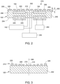
- FIG 2 illustrates a schematic cross-sectional detail view of the electrostatic chuck assembly 120 shown in Figure 1 .
- the body 202 may be fabricated from a dielectric material, such as a ceramic such as aluminum nitride and the like.
- the body 202 alternatively may be fabricated from plastic materials, such as from sheets of polyimide, polyether ether ketone, and the like.
- the body 202 has a backside surface 204 and a frontside surface 205.
- the frontside surface 205 is utilized to support the substrate 122.
- a wafer spacing mask 210 is formed on the frontside surface 205 to minimize the contact area between the substrate 122 and the electrostatic chuck assembly 120.
- the wafer spacing mask 210 may be integrally formed from the material comprising the body 202, or may be comprised of one or more separate layers of material deposited on the frontside surface 205 of the body 202.
- the wafer spacing mask 210 may have a top surface 208 and a bottom surface 206.
- the bottom surface 206 may be disposed directly upon the frontside surface 205 of the electrostatic chuck assembly 120.
- a thickness 260 of the wafer spacing mask 210 may be preferentially selected and spatially distributed across the frontside surface 205 to form features such as a plurality of mesas 215 and, optionally, an outer peripheral ring 225.
- the mesas 215 are generally configured to support the substrate 122 along the top surface 208 during processing.
- Gas passages 220 are formed between the mesas 215, allowing backside gas to be provided between the substrate 122 and the frontside surface 205 of the electrostatic chuck assembly 120.
- the outer peripheral ring 225 may be a solid ring or segments in a structure similar to the mesas 215 on the top surface 208 of the electrostatic chuck assembly 120, and utilized to confine or regulate the presence of the flow of backside gas from under the substrate 122 through the gas passages 220.
- the outer peripheral ring 225 is similar to the mesas 215 in shape and configuration. Alternately, the outer peripheral ring 225 may be utilized to center the substrate 122 on the electrostatic chuck assembly 120.
- a heat transfer gas source 230 is coupled through the electrostatic chuck assembly 120 to the frontside surface 205 to provide backside gas to the gas passages 220 defined between the mesas 215.
- the heat transfer gas source 230 provides a heat transfer gas (i.e., the backside gas) that flows between the backside of the substrate 122 and the electrostatic chuck assembly 120 in order to help regulate the rate of heat transfer between the electrostatic chuck assembly 120 and the substrate 122.
- the heat transfer gas may flow from outwards from a center of the electrostatic chuck assembly 120 and through the gas passages 220 around the mesas 215 and over the outer peripheral ring 225 into the processing volume 116 (shown in Figure 1 ).
- the heat transfer gas may comprise an inert gas, such as argon, helium, nitrogen, or a process gas.
- the heat transfer gas such as argon, may be a process gas, and wherein a flow rate into the chamber volume is measured to obtain predictable results.
- the heat transfer gas may be delivered to the gas passages 220 through one or more inlets 222 in the electrostatic chuck assembly 120 that are in fluid communication with one or more gas passages 220 and the heat transfer gas source 230.
- the outer peripheral ring 225 contacts the substrate near its edge and may be preferentially designed to control the amount of heat transfer gas that escapes from between the substrate 122 and the electrostatic chuck assembly 120 into the processing volume.
- the outer peripheral ring 225 and mesas 215 may be configured to provide a resistance to flow the transfer gas such that a pressure of the gas present between the substrate 122 and electrostatic chuck assembly 120 does not exceed a predetermined value.
- Temperature regulation of the body 202, and ultimately the substrate 122, may further be monitored and controlled using one or more cooling channels 245 disposed in a cooling plate 240 disposed in contact with the backside surface 204 of the body 202.
- the cooling channels 245 are coupled to and in fluid communication with a fluid source 250 that provides a coolant fluid, such as water, though any other suitable coolant fluid, whether gas or liquid, may be used.
- the wafer spacing mask 210 may be formed by depositing material through a mask onto the frontside surface 205.
- the use of a mask may allow better control of the size, shape, and distribution of features in the wafer spacing mask 210, thereby controlling the both the contact area of the mesas 215 and the conductance of the gas passages 220 defined between the mesas 215.
- each individual mesa 215 may generally have any suitable shape and height, each of which may be preferentially selected to fulfill particular design parameters (such as a desired chucking force and/or heat transfer).
- the top surface 208 of the mesas 215 of the wafer spacing mask 210 may form a planar surface.
- the top surface 208 of the mesas 215 of the wafer spacing mask 210 may form a non-planar surface, for example, a concave or convex surface.
- mesas 215 may have a mesa height 262 of about 1 micron to about 100 microns, or more preferably between about 1 micron and 30 microns.
- the surface of the mesas 215 that supports the substrate 122 may have a small rounded bump-like shape to minimize total contact area between the mesas 215 and the substrate 122.
- mesas 215 may include a small bump or protrusion atop a generally flat surface.
- the frontside surface 205 itself may vary between relative high and low points (similar to mesas 215 and gas passages 220), and wafer spacing mask 210 may be formed on this non-uniform surface.
- a non-uniform mask profile may be used to form the wafer spacing mask 210.
- the non-uniform mask profile may permit the height of each mesa 215 or depth of each gas passage 220 to be controlled individually or in combination.
- a wafer spacing mask 210 created using the non-uniform mask profile may advantageously provide a more uniform chucking force across a substrate.
- Figure 3 illustrates a schematic cross-sectional detail view of a wafer spacing mask deposited onto an electrostatic chuck assembly, according to one embodiment.
- the height of mesas 215 increase with lateral distance from a centerline 360 of the electrostatic chuck assembly 120, so that a maximum mesa height occurs at the outermost mesa 325, corresponding to outer peripheral ring 225.
- the heights of the mesas 215 may be at a minimum at mesas 315 most proximate the centerline 360.
- individual mesas 215 may have any suitable shape and the mask profile may be selected to provide mesas 215 having different sizes and/or shapes.
- the mask profile may provide for lateral symmetry so that corresponding mesas 215 at a particular lateral distance from centerline 360 have the same height and/or shape.
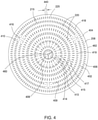
- Figure 4 illustrates a top view of the frontside surface 205 of the electrostatic chuck assembly 120.
- the frontside surface 205 of the electrostatic chuck assembly 120 has the wafer spacing mask 210 of deposited thereon.
- the frontside surface 205 of the electrostatic chuck assembly 120 can be characterized as having raised areas 402 defined by the wafer spacing mask 210 and unmodified areas 404 defined by the portions of the frontside surface 205 substantially uncovered by the wafer spacing mask 210.
- the unmodified areas 404 of the frontside surface 205 may include a layer of the same materials deposited to form the wafer spacing mask 210 which remains below the top surface 208 of the mesas 215 and defines the gas passages 220.
- the wafer spacing mask 210 may also include elongated features 406 that correspond to the mesas 215 of Figure 2 .
- the wafer spacing mask 210 may also include cylindrical features 408, and 410, and center tap features 414.
- the top surface 208 may also have lift pin hole openings 416.
- the cylindrical features 410 may be formed inward of the lift pin hole openings 416 in place of an elongated feature to locally reduce the substrate contact area and allow more gas flow to compensate for thermal non-uniformities caused by presence of the lift pin hole openings 416 extending through the body 202 of the electrostatic chuck assembly 120.
- the long axis of the elongated features 406 of the wafer spacing mask 210 may generally be radially aligned from a centerline 460 to an outer edge 462 of the electrostatic chuck assembly 120. Additionally, the rounded features 408, and 410 may also be radially aligned the elongated features 406 from the centerline 460 to the outer edge 462. An outermost ring 418 of mesas 215 may define the outer peripheral ring 225. Gas passages 220 are defined between the top surfaces 208 of the mesas 215 defining the wafer spacing mask 210. The gas passages 220 may also radially aligned from the centerline 460 to the outer edge 462 of the electrostatic chuck assembly 120, or may also extend in different directions, such as concentrically from the centerline 460 of the electrostatic chuck assembly 120.
- the elongated features 406 may be arranged in concentric rows 409 emanating from the center.
- each concentric row 409 has the same number of elongated features 406.
- the number of elongated features 406 in each of the concentric rows 409 may increase from the centerline 460 to the outer edge 462.
- the number of elongated features 406 in the row 409 nearest the outer edge 462 is greater than the number of elongated features 406 in the concentric row 409 nearest the centerline 460.
- the number of elongated features 406 may double in one or more subsequent concentric row 409.
- the number of elongated features 406 in a first row 413 may be half of the number of elongated features 406 in a second row 415.
- the number of elongated features 406 in the second row 415 may be half of number of elongated features 406 in a fourth row 417.
- the number of elongated features 406 in the fourth row 417 may be half of number of elongated features 406 in a sixth row 419. That is, the number of elongated features 406 may double in every other row 409 starting from the centerline 460 to the outer edge 462. In this manner, a spacing 440 between elongated features 406 in the rows 409 remains fairly consistent.
- the spacing 440 between adjacent elongated features 406 in a row 409 may have a lateral distance of about 0.1 inches to about 0.5 inches.
- the radial length of long axis of the elongated feature 406 may be within a range of about 0.1 inches to about 0.5 inches.
- the spacing between radially aligned elongated features 406 in adjacent rows 409 may be within a range of about 0.1 inches to about 0.5 inches.
- the material composition of the wafer spacing mask 210 may be preferentially selected based on several properties.
- the material composition for an improved top surface 208 may be selected to exhibit one or more of high hardness, a high modulus of elasticity, low coefficient of friction, and/or a low wear factor.
- the wafer spacing mask 210 may be fabricated from titanium nitride.
- the wafer spacing mask 210 may be fabricated from diamond-like carbon (DLC) compositions, such as DYLYN TM (a trademark of Sulzer Ltd.) and the like.
- DLC diamond-like carbon
- the radial aligned gas passages 220 and mesas 215 reduce the pressure of the backside gas flowing through the gas passages 220.
- the radial aligned gas passages 220 and mesas 215 promote the flow of the backside gas by reducing the conductance of the gas flow.
- the radial aligned gas passages 220 and mesas 215 may reduce the backside gas pressure at the outer edge 462 from non-radial aligned gas passages and mesas from about 50% to about 70%, such as about 64% at less than 10 SCCM flow rates on a 300 mm electrostatic chuck assembly 120 as compared to conventional electrostatic chuck assemblies not having radially aligned elongated features.
- the backside gas having a pressure of about 3 Torr and 3 SCCM at the inlet, such as inlet 222, and a pressure of about 7 Torr on the outer edge of a conventional ESC, having non-radial aligned mesas may have the pressure reduced to about 4 Torr on the ESC 120 having radial aligned gas passages 220 and mesas 215.
- the reduced pressure beneficially increases the velocity of the backside gas by about 100%.
- the backside gas having a pressure of about 3 Torr and 0.1 SCCM at an inlet, such as inlet 222, and a pressure of about 4 Torr on the outer edge of a conventional ESC, having non-radial aligned mesas may be able to reduce the pressure to about 2 Torr on the ESC 120 having radial aligned gas passages 220 and mesas 215.
- the reduced pressure beneficially increases the velocity of the backside gas by about 100%.
- the improved backside gas pressure and velocity promotes thermal uniformity of the substrate 122 disposed on the wafer spacing mask 210. Since the backside gas flows more freely, the backside gas is better able to regulate the temperature of the substrate 122 as heat is be transferred from the substrate 122 more readily.
- the radial aligned gas passages 220 and mesas 215 produce a backside gas pressure between about 2.5 Torr and about 8 Torr, such as 2.5 Torr, at the outer edge 462 when flowing about 0.1 SCCM of backside gas through the inlet 222 at a pressure of about 3 Torr.
- the radial aligned gas passages 220 and mesas 215 produce a backside gas pressure of about 4 Torr at the outer edge 462 when flowing about 3 SCCM of backside gas through the inlet 222 at a pressure of about 3 Torr.
- the maximum velocity of the backside gas at the outer edge 462 is between about 6 mm/s and about 1 mm/s, such as about 5.77 mm/s when flowing about 3 SCCM of backside gas through the inlet 222 into the gas passages 220. In one embodiment, the maximum velocity is 4 mm/s when a rate of 3 SCCM of backside gas is flowed into the inlet 222 at 3 Torr. In another embodiment, the maximum velocity is 1.31 mm/s when a rate of 21 SCCM of backside gas is flowed into the inlet 222 at 3 Torr.
- the maximum velocity of the backside gas at the outer edge 462 is between about 6 mm/s and about 1 mm/s, such as about 4 mm/s when flowing about 0.1 SCCM to about 1 SCCM of backside gas through the inlet 222 into the gas passages 220.
- the maximum velocity is 2.1 mm/s when a rate of 0.1 SCCM of backside gas is flowed into the inlet 222 at 3 Torr.
- the maximum velocity is 4.7 mm/s when a rate of 0.1 SCCM of backside gas is flowed into the inlet 222 at 3 Torr.
- the total area of top surface 208 of the wafer spacing mask 210 that is in contact with the substrate 122 is about 20 cm 2 to about 60 cm 2 , which is an increase in surface contact area of nearly three times greater than conventional wafer spacing masks.
- the increased contact area of the radial aligned mesas 215 increases the theoretical chucking force on the substrate from about 800 grams to about 3300 grams for the same chucking voltage.
- the addition contact area of the radial aligned gas passages 220 and mesas 215 with the substrate 122 reduce the overall stress on the substrate 122 significantly while the actual surface area of the electrostatic chuck assembly 120 in contact with substrate 122 is only between about 3% to about 15%.
- the radial aligned mesas 215 reduce the friction between the substrates 122 and the electrostatic chuck assembly 120.
- the radial aligned mesas 215 reduce wear and particle generation due to greater surface contact between the substrate 122 and the electrostatic chuck assembly 120.
- the greater contact area between the electrostatic chuck assembly 120 and the substrate 122 provides additional support to the substrate and thus lowers the overall stress across the substrate 122 from chucking the substrate 122.
- the electrostatic chuck assembly 120 having radial aligned mesas 215, may reduce the stress about 30% on the substrate 122 over a conventional electrostatic chuck assembly.
- the radial aligned mesas 215 reduce the temperature gradient from the centerline 460 to outer edge 462 of the substrate 122 as compared to a conventional electrostatic chuck assembly.
- the substrate 122 especially along the outside perimeter, experiences a reduction in the stress, from the increased contact area, and temperature gradient, from the decrease pressure and increase velocity of the backside gas, which may damage (i.e., crack) the substrate.
- the stress on the substrate 122 is dependent on not only the thermal gradient but also the material.
- a TTN film on the substrate 122 may be about 58 MPa at a time corresponding to the greatest temperature gradient in the film and then reach less than about 8 MPa after about 10 seconds.
- a DLC film on the substrate 122 may be about 50 MPa at a time corresponding to the greatest temperature gradient in the film and then reach less than about 11 MPa after about 10 seconds.
- the substrate 122 stress is maximum at a time step of about 0 seconds to about 1 second due to a maximum difference in the temperature at the initial time step.
- the fatigue stress on the substrate during 0 to 3 seconds is very critical , which will result in fracture of the material in contact, hence preheating the substrate and controlled landing of the substrate on the Electrostatic chuck are both very critical .
- Convective heating of the substrate by increasing the inlet temperature is a possibility during the substrate transport in to the change.
- the blades of the heater can also be actively maintained at elevated temperature based on the process recipe +/- 50 degree C to reduce the thermal shock and thermal transient fatigue stress on initial 3 second contact.
- the radially outward design of the mesas 215 and gas passages 220 on the frontside surface 205 of the electrostatic chuck assembly 120 improves thermal uniformity on substrates processed thereon.
- the radially outward design of the mesas 215 and gas passages 220 provide better control of backside gas for the electrostatic chuck assembly 120.
- the radially outward design of the mesas 215 and gas passages 220 promote reduced wear characteristics due to more surface area contact between the substrate 122 and the electrostatic chuck assembly 120.
- the radially outward design of the mesas 215 and gas passages 220 on the top surface 208 of the electrostatic chuck assembly 120 provides improved support to substrate backside due to improved contact area for reducing the stress, and subsequent damage, to the substrate 122.
- the disclosed embodiments of the present invention provide a pattern of features for an electrostatic chuck assembly that are directed toward providing reduced particle generation and reduced wear of substrates and chucking devices.
Landscapes
- Engineering & Computer Science (AREA)
- Chemical & Material Sciences (AREA)
- Microelectronics & Electronic Packaging (AREA)
- General Physics & Mathematics (AREA)
- Power Engineering (AREA)
- Computer Hardware Design (AREA)
- Manufacturing & Machinery (AREA)
- Physics & Mathematics (AREA)
- Condensed Matter Physics & Semiconductors (AREA)
- Organic Chemistry (AREA)
- Materials Engineering (AREA)
- Metallurgy (AREA)
- Chemical Kinetics & Catalysis (AREA)
- Mechanical Engineering (AREA)
- Container, Conveyance, Adherence, Positioning, Of Wafer (AREA)
- Drying Of Semiconductors (AREA)
Applications Claiming Priority (2)
| Application Number | Priority Date | Filing Date | Title |
|---|---|---|---|
| US14/616,647 US20160230269A1 (en) | 2015-02-06 | 2015-02-06 | Radially outward pad design for electrostatic chuck surface |
| PCT/US2016/012362 WO2016126360A1 (en) | 2015-02-06 | 2016-01-06 | Radially outward pad design for electrostatic chuck surface |
Publications (3)
| Publication Number | Publication Date |
|---|---|
| EP3254307A1 EP3254307A1 (en) | 2017-12-13 |
| EP3254307A4 EP3254307A4 (en) | 2018-08-15 |
| EP3254307B1 true EP3254307B1 (en) | 2022-03-02 |
Family
ID=56564492
Family Applications (1)
| Application Number | Title | Priority Date | Filing Date |
|---|---|---|---|
| EP16746928.7A Active EP3254307B1 (en) | 2015-02-06 | 2016-01-06 | Radially outward pad design for electrostatic chuck surface |
Country Status (7)
Families Citing this family (12)
| Publication number | Priority date | Publication date | Assignee | Title |
|---|---|---|---|---|
| US9646843B2 (en) * | 2014-12-08 | 2017-05-09 | Applied Materials, Inc. | Tunable magnetic field to improve uniformity |
| KR102669903B1 (ko) * | 2016-08-30 | 2024-05-28 | 주성엔지니어링(주) | 기판 처리 장치 |
| US20180148835A1 (en) | 2016-11-29 | 2018-05-31 | Lam Research Corporation | Substrate support with varying depths of areas between mesas and corresponding temperature dependent method of fabricating |
| US11469130B2 (en) | 2017-06-16 | 2022-10-11 | Jusung Engineering Co., Ltd. | Substrate processing apparatus and rotating electrical connector for vacuum |
| KR102359591B1 (ko) * | 2017-06-16 | 2022-02-08 | 주성엔지니어링(주) | 진공용 회전 전기 커넥터 |
| CN108538776B (zh) * | 2018-03-29 | 2021-11-16 | 北京北方华创微电子装备有限公司 | 静电卡盘及其制造方法 |
| SG11202010673RA (en) | 2018-06-22 | 2021-01-28 | Applied Materials Inc | Methods of minimizing wafer backside damage in semiconductor wafer processing |
| JP7134826B2 (ja) * | 2018-10-11 | 2022-09-12 | 東京エレクトロン株式会社 | 静電チャックの生産方法 |
| CN110158029B (zh) * | 2019-07-05 | 2020-07-17 | 北京北方华创微电子装备有限公司 | 掩膜结构和fcva设备 |
| KR20240042451A (ko) * | 2021-08-13 | 2024-04-02 | 샤인 테크놀로지스 엘엘씨 | 이온 및 동위원소 생산과 같은 고진공 응용을 위한 자기 회전 장치 |
| AU2022358410A1 (en) | 2021-10-01 | 2024-04-11 | Shine Technologies, Llc | Ion production system with fibrous lattice for ion collection |
| WO2024076562A1 (en) * | 2022-10-03 | 2024-04-11 | Applied Materials, Inc. | Web coating method and vented cooling drum with integral electrostatic clamping |
Family Cites Families (19)
| Publication number | Priority date | Publication date | Assignee | Title |
|---|---|---|---|---|
| US5646814A (en) * | 1994-07-15 | 1997-07-08 | Applied Materials, Inc. | Multi-electrode electrostatic chuck |
| US5825607A (en) * | 1996-05-08 | 1998-10-20 | Applied Materials, Inc. | Insulated wafer spacing mask for a substrate support chuck and method of fabricating same |
| JP3805134B2 (ja) * | 1999-05-25 | 2006-08-02 | 東陶機器株式会社 | 絶縁性基板吸着用静電チャック |
| JP3859937B2 (ja) * | 2000-06-02 | 2006-12-20 | 住友大阪セメント株式会社 | 静電チャック |
| US7161121B1 (en) * | 2001-04-30 | 2007-01-09 | Lam Research Corporation | Electrostatic chuck having radial temperature control capability |
| KR100422444B1 (ko) * | 2001-05-29 | 2004-03-12 | 삼성전자주식회사 | 정전 척에 설치되는 웨이퍼 공간 지지장치 및 그 제조방법 |
| US6946403B2 (en) * | 2003-10-28 | 2005-09-20 | Axcelis Technologies, Inc. | Method of making a MEMS electrostatic chuck |
| US7663860B2 (en) * | 2003-12-05 | 2010-02-16 | Tokyo Electron Limited | Electrostatic chuck |
| US7697260B2 (en) * | 2004-03-31 | 2010-04-13 | Applied Materials, Inc. | Detachable electrostatic chuck |
| JP5069452B2 (ja) * | 2006-04-27 | 2012-11-07 | アプライド マテリアルズ インコーポレイテッド | 二重温度帯を有する静電チャックをもつ基板支持体 |
| US8422193B2 (en) * | 2006-12-19 | 2013-04-16 | Axcelis Technologies, Inc. | Annulus clamping and backside gas cooled electrostatic chuck |
| JP2010521820A (ja) * | 2007-03-12 | 2010-06-24 | 東京エレクトロン株式会社 | 基板内での処理の均一性を改善するための動的な温度背面ガス制御 |
| US7576018B2 (en) * | 2007-03-12 | 2009-08-18 | Tokyo Electron Limited | Method for flexing a substrate during processing |
| US7667944B2 (en) * | 2007-06-29 | 2010-02-23 | Praxair Technology, Inc. | Polyceramic e-chuck |
| TWI475594B (zh) * | 2008-05-19 | 2015-03-01 | Entegris Inc | 靜電夾頭 |
| EP2321846A4 (en) * | 2008-08-12 | 2012-03-14 | Applied Materials Inc | ELECTROSTATIC FODDER ASSEMBLY |
| US8861170B2 (en) * | 2009-05-15 | 2014-10-14 | Entegris, Inc. | Electrostatic chuck with photo-patternable soft protrusion contact surface |
| NL2009189A (en) * | 2011-08-17 | 2013-02-19 | Asml Netherlands Bv | Support table for a lithographic apparatus, lithographic apparatus and device manufacturing method. |
| KR102042083B1 (ko) * | 2013-03-15 | 2019-11-27 | 어플라이드 머티어리얼스, 인코포레이티드 | 정전 척의 수리 및 복원을 위한 방법 및 장치 |
-
2015
- 2015-02-06 US US14/616,647 patent/US20160230269A1/en not_active Abandoned
-
2016
- 2016-01-06 CN CN202210254455.0A patent/CN114686834A/zh active Pending
- 2016-01-06 CN CN201680004654.9A patent/CN107208261A/zh active Pending
- 2016-01-06 EP EP16746928.7A patent/EP3254307B1/en active Active
- 2016-01-06 WO PCT/US2016/012362 patent/WO2016126360A1/en active Application Filing
- 2016-01-06 KR KR1020177024969A patent/KR102619126B1/ko active Active
- 2016-01-06 JP JP2017541608A patent/JP6711838B2/ja active Active
- 2016-01-08 TW TW105100585A patent/TWI685916B/zh active
Also Published As
| Publication number | Publication date |
|---|---|
| JP6711838B2 (ja) | 2020-06-17 |
| WO2016126360A1 (en) | 2016-08-11 |
| TW201637122A (zh) | 2016-10-16 |
| US20160230269A1 (en) | 2016-08-11 |
| EP3254307A4 (en) | 2018-08-15 |
| KR102619126B1 (ko) | 2023-12-27 |
| EP3254307A1 (en) | 2017-12-13 |
| CN114686834A (zh) | 2022-07-01 |
| KR20170110712A (ko) | 2017-10-11 |
| CN107208261A (zh) | 2017-09-26 |
| JP2018505561A (ja) | 2018-02-22 |
| TWI685916B (zh) | 2020-02-21 |
Similar Documents
| Publication | Publication Date | Title |
|---|---|---|
| EP3254307B1 (en) | Radially outward pad design for electrostatic chuck surface | |
| US9218997B2 (en) | Electrostatic chuck having reduced arcing | |
| US9068265B2 (en) | Gas distribution plate with discrete protective elements | |
| CN106935541B (zh) | 用于静电卡盘表面的垫设计 | |
| JP6149945B2 (ja) | 静電チャック装置 | |
| KR102825074B1 (ko) | 통합된 베벨 퍼지 기능 및 후면을 갖는 웨이퍼 가열기 | |
| KR20190095075A (ko) | 플라스마 처리 장치 | |
| JP2010027860A (ja) | フォーカスリング及び基板載置台、並びにそれらを備えたプラズマ処理装置 | |
| JP2023507091A (ja) | 端部/中央部の不均一性を軽減するためにウエハの外周近傍に凹部を備えた半導体処理チャック | |
| US11495483B2 (en) | Backside gas leakby for bevel deposition reduction | |
| US20240249924A1 (en) | Bipolar electrostatic chuck electrode designs | |
| TWI869158B (zh) | 可偏壓靜電吸盤 | |
| US11929278B2 (en) | Low impedance current path for edge non-uniformity tuning | |
| US20250125180A1 (en) | Bipolar electrostatic chuck electrode with self-induced dc voltage | |
| US20240203705A1 (en) | Surface topologies of electrostatic substrate support for particle reduction | |
| TW202527467A (zh) | 具有自感應dc電壓的雙極靜電吸盤電極 | |
| TW202527185A (zh) | 可偏壓靜電吸盤 | |
| KR20210131692A (ko) | 내식각성이 향상된 플라즈마 처리장치 |
Legal Events
| Date | Code | Title | Description |
|---|---|---|---|
| STAA | Information on the status of an ep patent application or granted ep patent |
Free format text: STATUS: THE INTERNATIONAL PUBLICATION HAS BEEN MADE |
|
| PUAI | Public reference made under article 153(3) epc to a published international application that has entered the european phase |
Free format text: ORIGINAL CODE: 0009012 |
|
| STAA | Information on the status of an ep patent application or granted ep patent |
Free format text: STATUS: REQUEST FOR EXAMINATION WAS MADE |
|
| 17P | Request for examination filed |
Effective date: 20170810 |
|
| AK | Designated contracting states |
Kind code of ref document: A1 Designated state(s): AL AT BE BG CH CY CZ DE DK EE ES FI FR GB GR HR HU IE IS IT LI LT LU LV MC MK MT NL NO PL PT RO RS SE SI SK SM TR |
|
| AX | Request for extension of the european patent |
Extension state: BA ME |
|
| DAV | Request for validation of the european patent (deleted) | ||
| DAX | Request for extension of the european patent (deleted) | ||
| A4 | Supplementary search report drawn up and despatched |
Effective date: 20180716 |
|
| RIC1 | Information provided on ipc code assigned before grant |
Ipc: H01L 21/683 20060101AFI20180710BHEP Ipc: H01L 21/67 20060101ALI20180710BHEP Ipc: H01L 21/687 20060101ALI20180710BHEP |
|
| REG | Reference to a national code |
Ref country code: DE Ref legal event code: R079 Ref document number: 602016069598 Country of ref document: DE Free format text: PREVIOUS MAIN CLASS: H01L0021683000 Ipc: H02N0013000000 |
|
| GRAP | Despatch of communication of intention to grant a patent |
Free format text: ORIGINAL CODE: EPIDOSNIGR1 |
|
| STAA | Information on the status of an ep patent application or granted ep patent |
Free format text: STATUS: GRANT OF PATENT IS INTENDED |
|
| RIC1 | Information provided on ipc code assigned before grant |
Ipc: H01L 21/687 20060101ALI20210211BHEP Ipc: C23C 14/50 20060101ALI20210211BHEP Ipc: H02N 13/00 20060101AFI20210211BHEP Ipc: H01L 21/683 20060101ALI20210211BHEP Ipc: H01L 21/67 20060101ALI20210211BHEP |
|
| INTG | Intention to grant announced |
Effective date: 20210304 |
|
| GRAJ | Information related to disapproval of communication of intention to grant by the applicant or resumption of examination proceedings by the epo deleted |
Free format text: ORIGINAL CODE: EPIDOSDIGR1 |
|
| STAA | Information on the status of an ep patent application or granted ep patent |
Free format text: STATUS: REQUEST FOR EXAMINATION WAS MADE |
|
| INTC | Intention to grant announced (deleted) | ||
| GRAS | Grant fee paid |
Free format text: ORIGINAL CODE: EPIDOSNIGR3 |
|
| STAA | Information on the status of an ep patent application or granted ep patent |
Free format text: STATUS: GRANT OF PATENT IS INTENDED |
|
| GRAP | Despatch of communication of intention to grant a patent |
Free format text: ORIGINAL CODE: EPIDOSNIGR1 |
|
| STAA | Information on the status of an ep patent application or granted ep patent |
Free format text: STATUS: GRANT OF PATENT IS INTENDED |
|
| INTG | Intention to grant announced |
Effective date: 20210818 |
|
| GRAA | (expected) grant |
Free format text: ORIGINAL CODE: 0009210 |
|
| STAA | Information on the status of an ep patent application or granted ep patent |
Free format text: STATUS: THE PATENT HAS BEEN GRANTED |
|
| AK | Designated contracting states |
Kind code of ref document: B1 Designated state(s): AL AT BE BG CH CY CZ DE DK EE ES FI FR GB GR HR HU IE IS IT LI LT LU LV MC MK MT NL NO PL PT RO RS SE SI SK SM TR |
|
| REG | Reference to a national code |
Ref country code: GB Ref legal event code: FG4D |
|
| REG | Reference to a national code |
Ref country code: CH Ref legal event code: EP Ref country code: AT Ref legal event code: REF Ref document number: 1473080 Country of ref document: AT Kind code of ref document: T Effective date: 20220315 |
|
| REG | Reference to a national code |
Ref country code: DE Ref legal event code: R096 Ref document number: 602016069598 Country of ref document: DE |
|
| REG | Reference to a national code |
Ref country code: IE Ref legal event code: FG4D |
|
| REG | Reference to a national code |
Ref country code: LT Ref legal event code: MG9D |
|
| REG | Reference to a national code |
Ref country code: NL Ref legal event code: MP Effective date: 20220302 |
|
| PG25 | Lapsed in a contracting state [announced via postgrant information from national office to epo] |
Ref country code: SE Free format text: LAPSE BECAUSE OF FAILURE TO SUBMIT A TRANSLATION OF THE DESCRIPTION OR TO PAY THE FEE WITHIN THE PRESCRIBED TIME-LIMIT Effective date: 20220302 Ref country code: RS Free format text: LAPSE BECAUSE OF FAILURE TO SUBMIT A TRANSLATION OF THE DESCRIPTION OR TO PAY THE FEE WITHIN THE PRESCRIBED TIME-LIMIT Effective date: 20220302 Ref country code: NO Free format text: LAPSE BECAUSE OF FAILURE TO SUBMIT A TRANSLATION OF THE DESCRIPTION OR TO PAY THE FEE WITHIN THE PRESCRIBED TIME-LIMIT Effective date: 20220602 Ref country code: LT Free format text: LAPSE BECAUSE OF FAILURE TO SUBMIT A TRANSLATION OF THE DESCRIPTION OR TO PAY THE FEE WITHIN THE PRESCRIBED TIME-LIMIT Effective date: 20220302 Ref country code: HR Free format text: LAPSE BECAUSE OF FAILURE TO SUBMIT A TRANSLATION OF THE DESCRIPTION OR TO PAY THE FEE WITHIN THE PRESCRIBED TIME-LIMIT Effective date: 20220302 Ref country code: ES Free format text: LAPSE BECAUSE OF FAILURE TO SUBMIT A TRANSLATION OF THE DESCRIPTION OR TO PAY THE FEE WITHIN THE PRESCRIBED TIME-LIMIT Effective date: 20220302 Ref country code: BG Free format text: LAPSE BECAUSE OF FAILURE TO SUBMIT A TRANSLATION OF THE DESCRIPTION OR TO PAY THE FEE WITHIN THE PRESCRIBED TIME-LIMIT Effective date: 20220602 |
|
| REG | Reference to a national code |
Ref country code: AT Ref legal event code: MK05 Ref document number: 1473080 Country of ref document: AT Kind code of ref document: T Effective date: 20220302 |
|
| PG25 | Lapsed in a contracting state [announced via postgrant information from national office to epo] |
Ref country code: PL Free format text: LAPSE BECAUSE OF FAILURE TO SUBMIT A TRANSLATION OF THE DESCRIPTION OR TO PAY THE FEE WITHIN THE PRESCRIBED TIME-LIMIT Effective date: 20220302 Ref country code: LV Free format text: LAPSE BECAUSE OF FAILURE TO SUBMIT A TRANSLATION OF THE DESCRIPTION OR TO PAY THE FEE WITHIN THE PRESCRIBED TIME-LIMIT Effective date: 20220302 Ref country code: GR Free format text: LAPSE BECAUSE OF FAILURE TO SUBMIT A TRANSLATION OF THE DESCRIPTION OR TO PAY THE FEE WITHIN THE PRESCRIBED TIME-LIMIT Effective date: 20220603 Ref country code: FI Free format text: LAPSE BECAUSE OF FAILURE TO SUBMIT A TRANSLATION OF THE DESCRIPTION OR TO PAY THE FEE WITHIN THE PRESCRIBED TIME-LIMIT Effective date: 20220302 |
|
| PG25 | Lapsed in a contracting state [announced via postgrant information from national office to epo] |
Ref country code: NL Free format text: LAPSE BECAUSE OF FAILURE TO SUBMIT A TRANSLATION OF THE DESCRIPTION OR TO PAY THE FEE WITHIN THE PRESCRIBED TIME-LIMIT Effective date: 20220302 |
|
| PG25 | Lapsed in a contracting state [announced via postgrant information from national office to epo] |
Ref country code: SM Free format text: LAPSE BECAUSE OF FAILURE TO SUBMIT A TRANSLATION OF THE DESCRIPTION OR TO PAY THE FEE WITHIN THE PRESCRIBED TIME-LIMIT Effective date: 20220302 Ref country code: SK Free format text: LAPSE BECAUSE OF FAILURE TO SUBMIT A TRANSLATION OF THE DESCRIPTION OR TO PAY THE FEE WITHIN THE PRESCRIBED TIME-LIMIT Effective date: 20220302 Ref country code: RO Free format text: LAPSE BECAUSE OF FAILURE TO SUBMIT A TRANSLATION OF THE DESCRIPTION OR TO PAY THE FEE WITHIN THE PRESCRIBED TIME-LIMIT Effective date: 20220302 Ref country code: PT Free format text: LAPSE BECAUSE OF FAILURE TO SUBMIT A TRANSLATION OF THE DESCRIPTION OR TO PAY THE FEE WITHIN THE PRESCRIBED TIME-LIMIT Effective date: 20220704 Ref country code: EE Free format text: LAPSE BECAUSE OF FAILURE TO SUBMIT A TRANSLATION OF THE DESCRIPTION OR TO PAY THE FEE WITHIN THE PRESCRIBED TIME-LIMIT Effective date: 20220302 Ref country code: CZ Free format text: LAPSE BECAUSE OF FAILURE TO SUBMIT A TRANSLATION OF THE DESCRIPTION OR TO PAY THE FEE WITHIN THE PRESCRIBED TIME-LIMIT Effective date: 20220302 Ref country code: AT Free format text: LAPSE BECAUSE OF FAILURE TO SUBMIT A TRANSLATION OF THE DESCRIPTION OR TO PAY THE FEE WITHIN THE PRESCRIBED TIME-LIMIT Effective date: 20220302 |
|
| PG25 | Lapsed in a contracting state [announced via postgrant information from national office to epo] |
Ref country code: IS Free format text: LAPSE BECAUSE OF FAILURE TO SUBMIT A TRANSLATION OF THE DESCRIPTION OR TO PAY THE FEE WITHIN THE PRESCRIBED TIME-LIMIT Effective date: 20220702 Ref country code: AL Free format text: LAPSE BECAUSE OF FAILURE TO SUBMIT A TRANSLATION OF THE DESCRIPTION OR TO PAY THE FEE WITHIN THE PRESCRIBED TIME-LIMIT Effective date: 20220302 |
|
| REG | Reference to a national code |
Ref country code: DE Ref legal event code: R097 Ref document number: 602016069598 Country of ref document: DE |
|
| PLBE | No opposition filed within time limit |
Free format text: ORIGINAL CODE: 0009261 |
|
| STAA | Information on the status of an ep patent application or granted ep patent |
Free format text: STATUS: NO OPPOSITION FILED WITHIN TIME LIMIT |
|
| PG25 | Lapsed in a contracting state [announced via postgrant information from national office to epo] |
Ref country code: DK Free format text: LAPSE BECAUSE OF FAILURE TO SUBMIT A TRANSLATION OF THE DESCRIPTION OR TO PAY THE FEE WITHIN THE PRESCRIBED TIME-LIMIT Effective date: 20220302 |
|
| 26N | No opposition filed |
Effective date: 20221205 |
|
| PG25 | Lapsed in a contracting state [announced via postgrant information from national office to epo] |
Ref country code: SI Free format text: LAPSE BECAUSE OF FAILURE TO SUBMIT A TRANSLATION OF THE DESCRIPTION OR TO PAY THE FEE WITHIN THE PRESCRIBED TIME-LIMIT Effective date: 20220302 |
|
| PG25 | Lapsed in a contracting state [announced via postgrant information from national office to epo] |
Ref country code: IT Free format text: LAPSE BECAUSE OF FAILURE TO SUBMIT A TRANSLATION OF THE DESCRIPTION OR TO PAY THE FEE WITHIN THE PRESCRIBED TIME-LIMIT Effective date: 20220302 |
|
| REG | Reference to a national code |
Ref country code: CH Ref legal event code: PL |
|
| GBPC | Gb: european patent ceased through non-payment of renewal fee |
Effective date: 20230106 |
|
| PG25 | Lapsed in a contracting state [announced via postgrant information from national office to epo] |
Ref country code: LU Free format text: LAPSE BECAUSE OF NON-PAYMENT OF DUE FEES Effective date: 20230106 |
|
| REG | Reference to a national code |
Ref country code: BE Ref legal event code: MM Effective date: 20230131 |
|
| PG25 | Lapsed in a contracting state [announced via postgrant information from national office to epo] |
Ref country code: LI Free format text: LAPSE BECAUSE OF NON-PAYMENT OF DUE FEES Effective date: 20230131 Ref country code: GB Free format text: LAPSE BECAUSE OF NON-PAYMENT OF DUE FEES Effective date: 20230106 Ref country code: CH Free format text: LAPSE BECAUSE OF NON-PAYMENT OF DUE FEES Effective date: 20230131 |
|
| PG25 | Lapsed in a contracting state [announced via postgrant information from national office to epo] |
Ref country code: BE Free format text: LAPSE BECAUSE OF NON-PAYMENT OF DUE FEES Effective date: 20230131 |
|
| PG25 | Lapsed in a contracting state [announced via postgrant information from national office to epo] |
Ref country code: IE Free format text: LAPSE BECAUSE OF NON-PAYMENT OF DUE FEES Effective date: 20230106 |
|
| PG25 | Lapsed in a contracting state [announced via postgrant information from national office to epo] |
Ref country code: MC Free format text: LAPSE BECAUSE OF FAILURE TO SUBMIT A TRANSLATION OF THE DESCRIPTION OR TO PAY THE FEE WITHIN THE PRESCRIBED TIME-LIMIT Effective date: 20220302 |
|
| PG25 | Lapsed in a contracting state [announced via postgrant information from national office to epo] |
Ref country code: MC Free format text: LAPSE BECAUSE OF FAILURE TO SUBMIT A TRANSLATION OF THE DESCRIPTION OR TO PAY THE FEE WITHIN THE PRESCRIBED TIME-LIMIT Effective date: 20220302 |
|
| PGFP | Annual fee paid to national office [announced via postgrant information from national office to epo] |
Ref country code: FR Payment date: 20241220 Year of fee payment: 10 |
|
| PGFP | Annual fee paid to national office [announced via postgrant information from national office to epo] |
Ref country code: DE Payment date: 20241218 Year of fee payment: 10 |
|
| PG25 | Lapsed in a contracting state [announced via postgrant information from national office to epo] |
Ref country code: CY Free format text: LAPSE BECAUSE OF FAILURE TO SUBMIT A TRANSLATION OF THE DESCRIPTION OR TO PAY THE FEE WITHIN THE PRESCRIBED TIME-LIMIT; INVALID AB INITIO Effective date: 20160106 |
|
| PG25 | Lapsed in a contracting state [announced via postgrant information from national office to epo] |
Ref country code: HU Free format text: LAPSE BECAUSE OF FAILURE TO SUBMIT A TRANSLATION OF THE DESCRIPTION OR TO PAY THE FEE WITHIN THE PRESCRIBED TIME-LIMIT; INVALID AB INITIO Effective date: 20160106 |