EP3248305B1 - Ethernet-switch für faseroptisches netzwerk - Google Patents
Ethernet-switch für faseroptisches netzwerk Download PDFInfo
- Publication number
- EP3248305B1 EP3248305B1 EP16703345.5A EP16703345A EP3248305B1 EP 3248305 B1 EP3248305 B1 EP 3248305B1 EP 16703345 A EP16703345 A EP 16703345A EP 3248305 B1 EP3248305 B1 EP 3248305B1
- Authority
- EP
- European Patent Office
- Prior art keywords
- transistor
- circuit
- signal
- wake
- power supply
- Prior art date
- Legal status (The legal status is an assumption and is not a legal conclusion. Google has not performed a legal analysis and makes no representation as to the accuracy of the status listed.)
- Active
Links
- 238000004891 communication Methods 0.000 claims description 29
- 239000003990 capacitor Substances 0.000 claims description 18
- 238000012545 processing Methods 0.000 claims description 11
- 239000000835 fiber Substances 0.000 claims description 10
- 238000000034 method Methods 0.000 claims description 6
- 230000008859 change Effects 0.000 claims description 5
- 230000008569 process Effects 0.000 claims description 5
- 230000008054 signal transmission Effects 0.000 claims description 2
- 239000013307 optical fiber Substances 0.000 description 31
- 230000003287 optical effect Effects 0.000 description 16
- 238000001514 detection method Methods 0.000 description 6
- 230000004913 activation Effects 0.000 description 5
- 230000005540 biological transmission Effects 0.000 description 4
- 230000009849 deactivation Effects 0.000 description 3
- 230000000694 effects Effects 0.000 description 3
- 230000008901 benefit Effects 0.000 description 2
- 230000005669 field effect Effects 0.000 description 2
- 238000012546 transfer Methods 0.000 description 2
- RYGMFSIKBFXOCR-UHFFFAOYSA-N Copper Chemical compound [Cu] RYGMFSIKBFXOCR-UHFFFAOYSA-N 0.000 description 1
- 238000013459 approach Methods 0.000 description 1
- 229910052802 copper Inorganic materials 0.000 description 1
- 239000010949 copper Substances 0.000 description 1
- 238000006073 displacement reaction Methods 0.000 description 1
- 238000007726 management method Methods 0.000 description 1
- 239000002184 metal Substances 0.000 description 1
- 229910052751 metal Inorganic materials 0.000 description 1
- 230000005693 optoelectronics Effects 0.000 description 1
- 230000008520 organization Effects 0.000 description 1
- 230000004044 response Effects 0.000 description 1
- 229920006395 saturated elastomer Polymers 0.000 description 1
- 230000035945 sensitivity Effects 0.000 description 1
- 230000009466 transformation Effects 0.000 description 1
- 230000002618 waking effect Effects 0.000 description 1
Images


Classifications
-
- H—ELECTRICITY
- H04—ELECTRIC COMMUNICATION TECHNIQUE
- H04Q—SELECTING
- H04Q11/00—Selecting arrangements for multiplex systems
- H04Q11/0001—Selecting arrangements for multiplex systems using optical switching
- H04Q11/0005—Switch and router aspects
-
- H—ELECTRICITY
- H04—ELECTRIC COMMUNICATION TECHNIQUE
- H04B—TRANSMISSION
- H04B10/00—Transmission systems employing electromagnetic waves other than radio-waves, e.g. infrared, visible or ultraviolet light, or employing corpuscular radiation, e.g. quantum communication
- H04B10/40—Transceivers
-
- H—ELECTRICITY
- H04—ELECTRIC COMMUNICATION TECHNIQUE
- H04Q—SELECTING
- H04Q11/00—Selecting arrangements for multiplex systems
- H04Q11/0001—Selecting arrangements for multiplex systems using optical switching
- H04Q11/0062—Network aspects
- H04Q11/0067—Provisions for optical access or distribution networks, e.g. Gigabit Ethernet Passive Optical Network (GE-PON), ATM-based Passive Optical Network (A-PON), PON-Ring
-
- H—ELECTRICITY
- H04—ELECTRIC COMMUNICATION TECHNIQUE
- H04Q—SELECTING
- H04Q11/00—Selecting arrangements for multiplex systems
- H04Q11/0001—Selecting arrangements for multiplex systems using optical switching
- H04Q11/0005—Switch and router aspects
- H04Q2011/0007—Construction
-
- H—ELECTRICITY
- H04—ELECTRIC COMMUNICATION TECHNIQUE
- H04Q—SELECTING
- H04Q11/00—Selecting arrangements for multiplex systems
- H04Q11/0001—Selecting arrangements for multiplex systems using optical switching
- H04Q11/0005—Switch and router aspects
- H04Q2011/0037—Operation
- H04Q2011/0039—Electrical control
Definitions
- the invention relates to an Ethernet switch for fiber optic network.
- the transit of information is mainly in the form of a light signal that travels along an optical fiber.
- the optical fiber makes it possible to pass a very large amount of information with a low attenuation.
- a computer or other communication equipment does not provide a light signal able to pass directly into an optical fiber.
- a computer delivers an electrical signal that passes through copper wires.
- This electrical signal into an optical signal is commonly done by a switch.
- a switch In an Ethernet environment, light information from an optical fiber is received by an Ethernet switch that will transmit the information to a plurality of devices, such as computers.
- the Ethernet switch is shared. In the same way, several Ethernet switches are connected to the same optical fiber in order to transit the maximum of available information.
- the document US2012 / 045202 discusses a low energy bi-directional receiver and its method of use.
- the circuit includes one or more power saving control circuits that will reduce the maximum power consumption during transceiver silence phases and are capable of switching portions of the transceiver between standard operating modes and energy saving modes. Such an embodiment allows only point energy savings over very short periods of time.
- the document US7,447,437 deals with an interface for the transfer of opto-electronic data.
- the circuit has a sleep mode when no activity is detected. A wake up signal is present during light detection to restore functionality.
- the subject of the invention is a media converter switch which has a lower power consumption than the devices of the prior art.
- the switch is notable in that it comprises a wake-up circuit connected to the first photodetector and to the communication port configured to generate an electric wake-up signal upon reception of a light signal by the first photodetector and / or a signal on the communication port, the wake-up circuit being connected to the power supply circuit to initiate power to the first light emitter and the communication port.
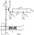
- the figure 1 shows a fiber optic network 1A, 1B, 1C and 1D which has several Ethernet switches 2A, 2B and 2C connected in series.
- a light signal arrives at the first Ethernet switch 2A from the optical fiber 1A and then passes through the first Ethernet switch 2A which re-transmits the light signal in the following optical fiber 1B to the second Ethernet switch 2B.
- the switches 2 must be constantly powered to detect the optical signal that arrives to process and / or reissue.
- the light signal arrives for example at the switch 2B where it is converted into an electrical signal to a terminal via a port 3 of electrical signal communication.
- the port 3 is configured to allow the transit of Ethernet connections.
- Port 3 is for example an RJ45 connector also called 8P8C.
- switch 2 can be broken down into several features.
- the switch comprises a first photodetector 4a which is configured to detect the light signal coming from the first optical fiber 1A.
- the first photodetector 4a will transform the light signal into an electrical signal.
- the switch 2 also comprises a first light emitter 5a which is configured to emit a light signal into the first optical fiber 1A.
- the first light emitter 5a will transform the electrical signal into a light signal.
- the first photodetector 4a and the first light emitter 5a are connected to a control circuit 6 which is configured to process the signals received by the first photodetector 4a and to define the signals to be emitted by the first light emitter 5a.
- the switch 2 also comprises one or more ports 3 for communication by electrical signals that can be embodied by jacks RJ45 standard.
- the switch 2 is connected to at least one terminal 6 which can be a computer and / or a camera via one or more communication ports 3.
- the information provided and / or received by the communication ports 3 is processed by the control circuit 7.
- the images captured by the camera are for example re-transmitted via the optical fiber for the end user who can in return send information triggering for example a displacement of the camera.
- the switch 2 further comprises a power supply circuit 8 which comprises a power source and / or a power supply terminal 8a intended to be connected to a power source.
- the power source 8 will supply the electrical energy to the first photodetector 4a, to the first light emitter 5a and to the control circuit 7.
- the switch further comprises a second photodetector 4b and a second light emitter 5b intended to be associated with a second optical fiber 1B.
- a light signal may be received from the first optical fiber 1A and retransmitted to the second optical fiber 1B and / or vice versa.
- the control circuit 7 comprises a processing circuit 9 configured to process electrical signals from the ports 3 and photodetectors 4 and to generate the electrical signals that will be sent on the ports 3 as well as on the light emitters 5.
- the processing circuit 9 is fed by the supply circuit 8.
- One way to limit the consumption of the Ethernet switch 2 is to provide a sleep mode in which some functions of the switch are disabled.
- switch 2 When switch 2 is in standby, no signal should be sent whether in electrical or optical form. It is therefore particularly advantageous not to supply the light emitters 5. It is also possible not to supply the circuit configured to emit the electrical signals. On the other hand, the circuits and elements involved in receiving the signals are fed in order to detect a re-entrant signal.
- the processing circuit 9 may not be powered or powered in part.
- a wake-up circuit 10 which will analyze the optical and electrical signals to initiate an awakening phase.
- a wake-up light signal is emitted on the first optical fiber to the first Ethernet switch 2.
- the wake-up light signal is received by the first photodetector 4a which will emit an electric wake-up signal to the ordered.
- the control circuit 7 and more particularly the wakeup circuit 10 will control the supply circuit 8 to supply again the light emitter 5a and / or 5b and the processing circuit 9.
- the new supply of the light emitter 5b will cause the emission of a wake-up signal on the second optical fiber 1B to destination of the second switch which causes the awakening of the second switch 2B.
- the wake-up signal includes information on the recipient of the information to be transmitted so that the control circuit 7 can determine whether the information waiting for it is intended or not. This information on the recipient avoids sending a wake-up signal to the next switch 2 while the information is not intended for him.
- This embodiment is particularly advantageous when the switch 2 has more than two connections to optical fibers which avoids transmitting a wake-up signal in an optical fiber unnecessarily.
- control circuit 7 may also be configured to engage the sleep mode when the photodetectors 4 do not detect a light signal for a predetermined period.
- the standby mode can be engaged if no incoming signal is received for more than one microsecond, preferably more than 3 microseconds, advantageously more than 5 microseconds.
- the control circuit 7 carries out the countdown of the predetermined period. If at the end of the count, no signal has been transmitted to the control circuit 7 it can engage the sleep mode.
- This functionality can be integrated into a standby circuit that can be implemented with the wake-up circuit 10 or in the power supply circuit 8.
- switches 2 engage the cascade sleep mode.
- a terminal 6 When a terminal 6 wants to exchange data with another terminal 6 via the network, it must transmit its information on the various optical fibers 1. This access to the network will initiate the awakening of the Ethernet switches 2.
- the wake-up signal is initiated by the terminal 6 by means of an electrical connection.
- the electrical connection connects the terminal 6 to the Ethernet switch 2 and more particularly to the port 3.
- the wake-up signal emitted by the terminal 6 comes to control a switch, for example a relay or a transistor which itself comes activate the light emitter 5 or simulate the reception of an optical signal by a photodetector 4.
- the port 3 is connected to the wake-up circuit 10 so that the reception of an electrical signal on the port 3 triggers the waking phase as described above.
- the terminal 6 when the terminal 6 has completed its communication, it informs the switch 2. If the switch 2 does not receive other light signals, it can cut off the power of the light emitters 5. The transmitter light 5 being off, no more signal passes and switches 2 will go to sleep cascade. Standby of switch 2 is performed if all signal receivers indicate that no signal is being received.
- the figure 3 illustrates a particular embodiment of detection of the awakening optical signal by the wakeup circuit 10.
- the photodetector 4 is polarized so as to transform a light signal into a representative current.
- the photodetector 4 is a photodiode.
- a first terminal of the photodetector 4 is connected to a first potential source which applies a first potential V1.
- a second terminal of the photodetector 4 is connected to the control circuit 7 which will process the electrical signals received and more particularly to the processing circuit 9.
- a transimpedance amplifier 11 is arranged between the photodetector 4 and the processing circuit 9 so as to shape the signal from the photodetector 4 and polarize the photodetector 4.
- the transimpedance amplifier is configured to apply a voltage V REF .
- the amplifier transforms the current signal delivered by the photodetector into a voltage signal which will be processed by the processing circuit 9 in a logical manner. It is advantageous to use a feedback resistance of the amplifier and thereby form a resistive transimpedance amplifier type device.
- the switch 2 comprises a wake-up circuit 10 which is configured to detect an electrical signal emitted by the photodetector 4 in response to a received light signal.
- the wake-up circuit 10 is connected between the photodetector and the potential source V1 to recover an electrical signal representative of the optical signals received.
- the wake-up circuit 10 is connected to the first terminal of the photodetector 4.
- the wake-up circuit 10 will transmit information that will initiate the awakening of the switch 2. This information is advantageously transmitted directly to the supply circuit 8.
- a first transistor T1 having a control electrode connected to the photodetector 4 so that the current emitted by the photodetector 4 changes the current delivered by the transistor T1.
- the signal at the output of the transistor T1 therefore changes according to the received light signal.
- the transistor reaches saturation as soon as receiving a signal by the photodetector so that the signal at the output of the transistor is of logic type, that is to say with the delivery of a 1 or a 0.
- the received light signal is transformed into a signal logic at the output of transistor T1.
- a first capacitor C1 is connected between the output of the first transistor T1 and the supply circuit 8 in association with a first resistor R4 so that the current delivered by the transistor T1 generates a current pulse forming a wake-up signal for the supply circuit 8.
- the current emitted by the transistor T1 is transformed into a current pulse which will form the wake-up signal to the supply circuit 8.
- the wake-up circuit 10 comprises a transistor T1 biased between second and third potential sources which respectively apply the potentials V2 and V3.
- the first terminal of the transistor T1 is connected to the second potential source V2 and the second terminal of the transistor T1 is connected to the third potential source V3.
- the control electrode of the transistor T1 is connected to the photodetector 4 so that the current flowing through the transistor T1 changes as a function of the current emitted by the photodetector 4.
- a second resistor R2 is disposed between the third potential source V3 and the second terminal of the transistor T1.
- the second terminal of the transistor T1 is connected to a third resistor R3 via a first capacitor C1.
- a first terminal of the first capacitor C1 is connected to the photodetector 4 and a second terminal of the first capacitor C1 is connected to the third resistor R3.
- the third resistor R3 is connected to the fourth potential source V4.
- the second terminal of the capacitor C1 and the terminal of the resistor R3 are connected to the supply circuit 8 to provide it with the electric wake-up command.
- connection 12 is made between the second terminal of the photodetector 4 or the first terminal of the capacitor C1 and the supply circuit 8. This connection makes it possible to send an electrical signal representative of the received light signal to the supply circuit 10.
- the first terminal of the photodetector 4 is connected to the potential source V1, advantageously via a resistor R1.
- the control electrode of the transistor T1 is connected between the potential source V1 and the other terminal of the photodetector 4.
- the signal detected by the photodetector 4 results in the emission of a current representative of the emitted signal.
- the current emitted by the photodetector 4 passes through the first resistor R1 and it modifies the intensity of the current delivered by the transistor T1.
- the current delivered by the transistor T1 to the assembly formed by the capacitor C1 and the resistor R3 will generate a pulse that will be detected by the supply circuit 8 as the wake-up signal of the switch 2.
- the transistor T1 is a bipolar transistor whose base electrode is connected to the photodetector 4. It is also advantageous to provide that the bipolar transistor T1 will be in a state of saturation when current flows through the photodetector. In this way the collector electrode will get closer to the value of the third potential.
- the ratio R1 / R2 and the current gain of the transistor T1 make it possible to set a detected optical power threshold beyond which the transistor T1 is saturated.
- the current emitted by the photodetector also reaches a threshold which will saturate the transistor T1
- a pulse is sent by the capacitor C1 and the line 12 passes to the high state. Line 12 remains high as long as the received optical power is above the threshold value.
- This arrangement makes it possible to form a logic signal from the received light signal. This electrical signal is different from the signal sent to the circuit 9.
- a field effect transistor T1 is usable.
- the resistor R1 acts as a resistor to the potential of the first source V1 which allows to cancel at least partly the leakage currents of the transistor T1.
- the second terminal of the transistor T1 is directly connected to the supply circuit 8 by the line 12.
- a light emitter When a light emitter is powered, it generates optical power, this power is read by the photodetector 4.
- the photodetector 4 emits a current representative of the activation of the optical fiber 1, which results in the transmission of the corresponding signal on the line 12.
- the line 12 indicates to the wake-up circuit as well as to the Standby circuit that the optical fiber is activated. When the fiber is no longer activated, the signal emitted by the line 12 for the circuit 8 changes.
- the standby circuit may initiate a standby switch or more particularly the portion of the switch that is associated with the deactivated optical fiber.
- the wake-up circuit also serves as a standby circuit. Alternatively, it is possible to connect the line 12 to the standby circuit.
- the capacitor C1 and the resistor R3 are not used.
- the photodetector 4 detects the activation of the optical fiber and the wake-up signal is emitted by the transistor T1 which reaches saturation. In this way, the activation of the optical fiber causes the activation of the line 12 and the awakening of the switch. Deactivation of the optical fiber causes deactivation of line 12 and possibly switching the switch off. In other words, as long as signals are received by the photodetector 4, the photodetector 4 sends a current and the transistor T1 does the same.
- the supply circuit 8 then receives a signal representative of the activity of the photodetector 4. When the optical signals stop, the photodetector 4 no longer emits current and this absence of an electrical signal is received by the supply circuit 8 which can put the switch to sleep.
- the detection threshold of the photodetector 4 By judiciously choosing the values of the first and second resistors R1 and R2, it is possible to set the detection threshold of the photodetector 4. For example, it is possible to use a resistor R1 having a value of 220KOhms and a resistor R2 having a value of 100KOhms so as to fix that the current resulting in the saturation of the transistor T1 is obtained for a threshold detection of the photodetector of the order of -24dBm (4 ⁇ Watt).
- the consumption of the photodetector 4 is equal to its dark current which is very low. It is also particularly advantageous to turn off the power of the processing circuit 9 to reduce the consumption of the switch 2 while ensuring the reception and processing of incoming electrical signals.
- the wake-up circuit 10 comprises a connection to one of the communication ports 3 by electrical signals.
- the wake-up circuit 10 comprises a first reception input of a wake-up signal formed for example by the port 3. This first input is connected to a fifth potential source V5 via a fourth resistor R4.
- a second transistor T2 is biased between a sixth potential source V6 and a seventh potential source V7.
- the control electrode of the second transistor T2 is connected to the first input.
- the first terminal of the transistor T2 is connected to the sixth potential source V6.
- the second terminal of the transistor is connected to the seventh potential source V7 via a fifth resistor R5.
- the second terminal of transistor T2 is connected to a sixth resistor R6 via a second capacitor C2.
- a first terminal of the capacitor C2 is connected to the second terminal of the transistor T2.
- the second terminal of the capacitor C2 is connected to the sixth resistor R6 and to the supply circuit.
- the operation of transistor T2 is advantageously identical to that of transistor T1 in order to output a logic signal of type 1 or 0.
- the sixth resistor R6 is connected to an eighth potential source V8.
- the second terminal of transistor T2 is connected directly to supply circuit 8 via line 13.
- the first input terminal is placed at a predetermined potential different from the potential V5, for example ground.
- a current then flows through the fourth resistor R4.
- a current is generated on the second terminal of the transistor T2.
- This current generated by the transistor T2 charges the second capacitor C2 which in combination with the sixth resistor R6 will create a pulse which is detected by the supply circuit 8 as a wake-up signal of the switch.
- the pulse represents the wake-up electrical signal which indicates to the power supply circuit 8 that the terminal 6 wants to transmit information via the optical fiber.
- the transistor T2 is advantageously a bipolar transistor whose base electrode is connected to the first input terminal. It is also advantageous to provide that the current flowing through the fourth resistor R4 will cause the saturation of the transistor T2 so that the potential present on the collector electrode will be close to the fifth potential. Alternatively, it is also possible to use a field effect transistor.
- the resistor R4 will act as a resistor to the potential V5 and will at least partially cancel the leakage currents of the transistor T2.
- a direct connection 13 between the second transistor T2 and the supply circuit 8 is particularly advantageous when the supply circuit 8 is configured to manage the supply of the various functions of the switch according to the signals sent by the terminal 6.
- the operating mode of the line 13 is identical to that described for the line 12. It is the same for the RC circuit formed by the capacitor C2 and the resistor R6 which is as advantageous as the RC circuit formed by capacitor C1 and resistor R3
- the first input terminal is on average at the preset potential and the transistor T2 sends a current.
- the direct connection between the transistor T2 and the supply circuit 8 is in the high state representative of a transfer of data from the user.
- the average value is calculated on a time base of a few milliseconds, for example 1 millisecond, advantageously between 2 and 5 milliseconds.
- the transistor T2 When the data flow stops, the transistor T2 no longer emits current and the direct connection between the transistor T2 and the control circuit goes to the state low.
- the power supply circuit 8 detects the change of state and can initiate the standby of the switch 2.
- the supply circuit 8 is advantageously configured not to supply the electrical communication port 3 or the first light emitter when the first and second direct connections 12, 13 are in the low state.
- the first input terminal is connected to a coil which connects the transit lines of the received signals represented by Rx + and Rx-.
- the first input terminal is at the preset potential.
- the potential of the first input terminal changes and the control circuit is able to detect the stop of the data transmission.
- This embodiment is particularly advantageous for passing the wake-up signal via the common mode of the cable communication pairs materialized by Rx + and Rx-. The advantage of passing the wake-up signal through the metal lines receiving the Rx + and Rx- signals is to locate the activity detection on the optical ports that emit optical power as soon as they are active.
- the wake-up signal is introduced into the communication pairs Tx + and Tx- and it transits to the terminal where it is dissociated, for example according to the previous embodiment, in the communication pairs Rx + and Rx. -.
- control electrode of the second transistor T2 is connected to a device configured to extract the common mode from the lines of the Rx + and Rx- communications used for the transmission of signals from the terminal 6. to switch 2.
Landscapes
- Engineering & Computer Science (AREA)
- Computer Networks & Wireless Communication (AREA)
- Physics & Mathematics (AREA)
- Electromagnetism (AREA)
- Signal Processing (AREA)
- Optical Communication System (AREA)
- Electronic Switches (AREA)
Claims (7)
- Ethernet-Switch (2) für Glasfasernetze (1), der umfasst:- einen ersten Lichtemitter (5a), der zum Übertragen eines Lichtsignals in der Glasfaser (1) vorgesehen ist,- einen ersten Fotodetektor (4a), der so vorgesehen ist, dass er ein von der Glasfaser (1) kommendes Lichtsignal in ein elektrisches Signal umwandelt,- mindestens einen Port (3) zur Kommunikation elektrischer Signale mit einem Endgerät (6),- eine Versorgungsschaltung (8), die so vorgesehen ist, dass sie den ersten Lichtemitter (5a) und den ersten Fotodetektor (4a) versorgt,- eine Aufweckschaltung (10), die an den ersten Fotodetektor (4a) und an den Kommunikationsport (3) gelegt und so vorgesehen ist, dass sie beim Empfang eines Lichtsignals durch den ersten Fotodetektor (4a) und/oder eines elektrischen Signals am Kommunikationsport (3) ein elektrisches Aufwecksignal erzeugt, wobei die Aufweckschaltung (10) an die Versorgungsschaltung (8) gelegt ist, um die Versorgung des ersten Lichtsenders (5a) und des Kommunikationsports (3) auszulösen,und dadurch gekennzeichnet, dass die Aufweckschaltung (10) umfasst:- einen ersten Transistor (T1) mit einer Steuerelektrode, die an den ersten Fotodetektor (4a) gelegt ist, sodass der vom ersten Fotodetektor (4a) abgegebene Strom dafür sorgt, dass sich der vom ersten Transistor (T1) abgegebene Strom fortbewegt,- einen ersten Kondensator (C1), der zwischen den Ausgang des ersten Transistors (T1) und die Versorgungsschaltung (8) in Verbindung mit einem ersten Widerstand (R4) so gelegt ist, dass der vom ersten Transistor (T1) gelieferte Strom einen Stromimpuls erzeugt, der ein Aufwecksignal für die Versorgungsschaltung (8) bildet.
- Ethernet-Switch (1) nach Anspruch 1, dadurch gekennzeichnet, dass er eine Verarbeitungsschaltung (9) umfasst, die von der Versorgungsschaltung (8) versorgt wird und so vorgesehen ist, dass sie elektrische Signale verarbeitet, die von den Kommunikationsports (3) und den Fotodetektoren (4) kommen, und um elektrische Signale zu erzeugen, die an die Ports (3) und die Lichtemitter (5) geschickt werden, sowie dadurch, dass die Aufweckschaltung (10) mit der Versorgungsschaltung (8) verbunden ist, um die Versorgung der Verarbeitungsschaltung (9) auszulösen.
- Ethernet-Switch nach einem der Ansprüche 1 und 2, dadurch gekennzeichnet, dass die Aufweckschaltung (10) eine erste Direktverbindung (12) zwischen dem Ausgang des ersten Transistors (T1) und der Versorgungsschaltung (8) umfasst.
- Ethernet-Switch nach einem der Ansprüche 1 und 2, dadurch gekennzeichnet, dass die Aufweckschaltung (10) umfasst:- einen zweiten Transistor (T2) mit einer Steuerelektrode, die an einen Kommunikationsport (3) zur elektrischen Kommunikation gelegt ist, in der Weise, dass das am Kommunikationsport (3) anliegende Potenzial dafür sorgt, dass sich die von dem zweiten Transistor (T2) gelieferte Stromstärke bewegt,- einen ersten Kondensator, der zwischen dem Ausgang des zweiten Transistors (T2) und der Versorgungsschaltung (8) in Verbindung mit einem zweiten Widerstand (R6) so geschaltet ist, dass der vom zweiten Transistor (T2) gelieferte Strom einen Stromimpuls erzeugt, der ein Aufwecksignal für die Versorgungsschaltung (8) bildet.
- Ethernet-Switch nach einem der Ansprüche 1, 2 und 4, dadurch gekennzeichnet, dass die Aufweckschaltung (10) eine zweite Direktverbindung (13) zwischen dem Ausgang des zweiten Transistors (T2) und der Versorgungsschaltung (8) umfasst.
- Ethernet-Schalter nach den Ansprüchen 3 und 5, dadurch gekennzeichnet, dass die Versorgungsschaltung (8) so vorgesehen ist, dass sie weder den elektrischen Kommunikationsport (3) noch den ersten Lichtemitter (5a) versorgt, wenn die erste und zweite Direktverbindung (12, 13) auf LOW stehen.
- Ethernet-Switch nach Anspruch 4, dadurch gekennzeichnet, dass die Steuerelektrode des zweiten Transistors (T2) an eine Vorrichtung gelegt ist, die so vorgesehen ist, dass sie den gemeinsamen Modus der Kommunikationsleitungen (Rx+, Rx-) herauszieht, die zur Übertragung von Signalen von dem Endgerät (6) zum Switch (2) verwendet werden.
Applications Claiming Priority (2)
| Application Number | Priority Date | Filing Date | Title |
|---|---|---|---|
| FR1550404A FR3031856B1 (fr) | 2015-01-19 | 2015-01-19 | Commutateur ethernet pour reseau en fibre optique. |
| PCT/FR2016/050093 WO2016116690A1 (fr) | 2015-01-19 | 2016-01-19 | Commutateur éthernet pour réseau en fibre optique |
Publications (2)
| Publication Number | Publication Date |
|---|---|
| EP3248305A1 EP3248305A1 (de) | 2017-11-29 |
| EP3248305B1 true EP3248305B1 (de) | 2018-12-05 |
Family
ID=52988285
Family Applications (1)
| Application Number | Title | Priority Date | Filing Date |
|---|---|---|---|
| EP16703345.5A Active EP3248305B1 (de) | 2015-01-19 | 2016-01-19 | Ethernet-switch für faseroptisches netzwerk |
Country Status (8)
| Country | Link |
|---|---|
| US (1) | US10547919B2 (de) |
| EP (1) | EP3248305B1 (de) |
| JP (1) | JP6685310B2 (de) |
| CN (1) | CN107534493B (de) |
| BR (1) | BR112017015365B1 (de) |
| CA (1) | CA2974284C (de) |
| FR (1) | FR3031856B1 (de) |
| WO (1) | WO2016116690A1 (de) |
Families Citing this family (4)
| Publication number | Priority date | Publication date | Assignee | Title |
|---|---|---|---|---|
| EP3643003B1 (de) | 2017-06-22 | 2020-10-14 | Signify Holding B.V. | Verbessertes glasfaser-poe-netzwerk |
| FR3070938B1 (fr) * | 2017-09-14 | 2019-08-23 | Psa Automobiles Sa | Systeme de gestion d’un reseau ethernet sur fibre optique d’un vehicule |
| CN111865424B (zh) * | 2020-05-25 | 2022-01-11 | 深圳市周立功单片机有限公司 | 一种汽车光纤以太网通信装置 |
| US20240178914A1 (en) * | 2022-11-29 | 2024-05-30 | Harris Global Communications, Inc. | Radio frequency over omni-directional free space optics |
Family Cites Families (8)
| Publication number | Priority date | Publication date | Assignee | Title |
|---|---|---|---|---|
| US6810216B1 (en) * | 1999-07-02 | 2004-10-26 | Nokia Corporation | Fast infrared transceiver with reduced power consumption |
| US7447437B2 (en) * | 2004-06-09 | 2008-11-04 | Infineon Technologies Fiber Optics Gmbh | Interface arrangement for opto-electronic data transfer, and plug-in opto-electronic transceiver |
| KR100932908B1 (ko) * | 2007-10-23 | 2009-12-21 | 한국전자통신연구원 | 광 액세스 망에서 광망 종단 장치 및 광 회선 단말의 전력절감 방법 |
| US20120030320A1 (en) * | 2010-07-30 | 2012-02-02 | Broadcom Corporation | Network power management |
| US20120045202A1 (en) * | 2010-08-17 | 2012-02-23 | Xu Jiang | High Speed Bi-Directional Transceiver, Circuits and Devices Therefor, and Method(s) of Using the Same |
| US8699885B2 (en) * | 2011-05-12 | 2014-04-15 | Cortina Systems, Inc. | Power control in an optical network unit |
| CN102725997B (zh) * | 2011-12-09 | 2016-11-23 | 华为技术有限公司 | 数据交换设备低功耗实现方法及其装置和数据交换设备 |
| CN103227758B (zh) * | 2013-03-25 | 2016-01-20 | 深圳市三旺通信技术有限公司 | 一种光纤以太网交换机及控制方法 |
-
2015
- 2015-01-19 FR FR1550404A patent/FR3031856B1/fr not_active Expired - Fee Related
-
2016
- 2016-01-19 CA CA2974284A patent/CA2974284C/fr active Active
- 2016-01-19 BR BR112017015365-3A patent/BR112017015365B1/pt active IP Right Grant
- 2016-01-19 WO PCT/FR2016/050093 patent/WO2016116690A1/fr active Application Filing
- 2016-01-19 JP JP2017537967A patent/JP6685310B2/ja active Active
- 2016-01-19 EP EP16703345.5A patent/EP3248305B1/de active Active
- 2016-01-19 CN CN201680010251.5A patent/CN107534493B/zh active Active
- 2016-01-19 US US15/544,664 patent/US10547919B2/en active Active
Non-Patent Citations (1)
| Title |
|---|
| None * |
Also Published As
| Publication number | Publication date |
|---|---|
| CA2974284C (fr) | 2022-08-30 |
| BR112017015365B1 (pt) | 2023-12-19 |
| JP6685310B2 (ja) | 2020-04-22 |
| CN107534493B (zh) | 2020-11-10 |
| FR3031856A1 (fr) | 2016-07-22 |
| FR3031856B1 (fr) | 2017-02-10 |
| US20180014094A1 (en) | 2018-01-11 |
| BR112017015365A2 (pt) | 2018-01-16 |
| JP2018507610A (ja) | 2018-03-15 |
| EP3248305A1 (de) | 2017-11-29 |
| US10547919B2 (en) | 2020-01-28 |
| CA2974284A1 (fr) | 2016-07-28 |
| WO2016116690A1 (fr) | 2016-07-28 |
| CN107534493A (zh) | 2018-01-02 |
Similar Documents
| Publication | Publication Date | Title |
|---|---|---|
| EP3248305B1 (de) | Ethernet-switch für faseroptisches netzwerk | |
| EP0709254B1 (de) | Elektronisches Informationsübertragungssystem auf stromführenden Leitungen, insbesonders für ein Kraftfahrzeug | |
| EP0052536B1 (de) | Sendermodul-Ausgangsleistungsstabilisierungsanordnung für ein Lichtwellenleiter-Übertragungssystem | |
| EP0034957A1 (de) | Vorrichtung zur automatischen Regulierung der Ausgangsleistung eines Sendermoduls für ein Übertragungssystem mit optischen Fasern | |
| EP0004815A2 (de) | Verfahren zum Übertragen elektrischer Signale mittels optischer Verbindung und Vorrichtung zur automatischen Verstärkungsregelung eines an der optischen Verbindung gekuppelten Empfangsweges | |
| EP0369833A1 (de) | Zugriffseinheit für einen Übertragungsweg eines lokalen Netzes | |
| FR2511824A1 (fr) | Systeme emetteur-recepteur de transmission numerique par voie optique et a debit variable | |
| EP0194177B1 (de) | Teilnehmerschnittstellenschaltung mit Überwachungsbetrieb bei verringerter Speisung | |
| EP0034082A2 (de) | Vorrichtung zur Alarmauslösung im Falle eines ungenügenden Übertragungspegels für den Empfängermodul eines Übertragungssystems mit optischen Fasern | |
| EP0566464A1 (de) | Quelle für optische Pulse und optisches Solitonübertragungssystem mit dieser Quelle | |
| FR2812987A1 (fr) | Procede, dispositif et systeme de commutation de lignes d'alimentation en energie electrique | |
| CH637779A5 (fr) | Detecteur photoelectrique. | |
| EP4059160A1 (de) | Drahtlose optische kommunikationsvorrichtung | |
| EP0014634A1 (de) | Aktive Kopplungsanordnung zwischen einer optischen Bus-Leitung und einem der Teilnehmern und Bus-Leitung, die solche Kopplungsanordnungen enthält | |
| EP0002971A1 (de) | Kopplungsanordnung für eine optische Übertragungsleitung und solche Anordnungen enthaltendes Übertragungssystem | |
| EP0962869A1 (de) | Zwei-Standard-Schnittstellenschaltung für serielle Verbindung | |
| EP0112227B1 (de) | Einrichtung zum Unterdrücken von Auswirkungen der thermischen Zeitkonstanten bei einer Anordnung mit lichtemittierender Diode | |
| CA2399165A1 (fr) | Procede et dispositif pour l'attribution automatique d'adresses a une pluralite de modules interconnectes par un reseau de communication a topologie complexe | |
| JPH0575544A (ja) | 自動利得調整回路 | |
| EP0961422B1 (de) | Optischer Sender mit mehreren optischen Quellen | |
| WO2022264028A1 (fr) | Dispositif de contrôle de l'émission/réception d'un point d'accès d'un réseau optique non filaire | |
| EP4213413B1 (de) | Empfangsvorrichtung, system, empfangsverfahren und lichtsignalkommunikationsverfahren | |
| EP4238244A1 (de) | Diskrete optoelektronische vorrichtung für einen zugangspunkt oder ein endgerät eines drahtlosen optischen netzwerks | |
| FR3062266A1 (fr) | Transpondeur pour la transmission de donnees dans le proche infrarouge | |
| FR2661793A1 (fr) | Systeme de transmission de donnees entre un frontal et des terminaux. |
Legal Events
| Date | Code | Title | Description |
|---|---|---|---|
| STAA | Information on the status of an ep patent application or granted ep patent |
Free format text: STATUS: THE INTERNATIONAL PUBLICATION HAS BEEN MADE |
|
| PUAI | Public reference made under article 153(3) epc to a published international application that has entered the european phase |
Free format text: ORIGINAL CODE: 0009012 |
|
| STAA | Information on the status of an ep patent application or granted ep patent |
Free format text: STATUS: REQUEST FOR EXAMINATION WAS MADE |
|
| 17P | Request for examination filed |
Effective date: 20170718 |
|
| AK | Designated contracting states |
Kind code of ref document: A1 Designated state(s): AL AT BE BG CH CY CZ DE DK EE ES FI FR GB GR HR HU IE IS IT LI LT LU LV MC MK MT NL NO PL PT RO RS SE SI SK SM TR |
|
| AX | Request for extension of the european patent |
Extension state: BA ME |
|
| DAV | Request for validation of the european patent (deleted) | ||
| DAX | Request for extension of the european patent (deleted) | ||
| GRAP | Despatch of communication of intention to grant a patent |
Free format text: ORIGINAL CODE: EPIDOSNIGR1 |
|
| STAA | Information on the status of an ep patent application or granted ep patent |
Free format text: STATUS: GRANT OF PATENT IS INTENDED |
|
| INTG | Intention to grant announced |
Effective date: 20180618 |
|
| GRAS | Grant fee paid |
Free format text: ORIGINAL CODE: EPIDOSNIGR3 |
|
| GRAA | (expected) grant |
Free format text: ORIGINAL CODE: 0009210 |
|
| STAA | Information on the status of an ep patent application or granted ep patent |
Free format text: STATUS: THE PATENT HAS BEEN GRANTED |
|
| AK | Designated contracting states |
Kind code of ref document: B1 Designated state(s): AL AT BE BG CH CY CZ DE DK EE ES FI FR GB GR HR HU IE IS IT LI LT LU LV MC MK MT NL NO PL PT RO RS SE SI SK SM TR |
|
| REG | Reference to a national code |
Ref country code: GB Ref legal event code: FG4D Free format text: NOT ENGLISH |
|
| REG | Reference to a national code |
Ref country code: CH Ref legal event code: EP |
|
| REG | Reference to a national code |
Ref country code: AT Ref legal event code: REF Ref document number: 1074395 Country of ref document: AT Kind code of ref document: T Effective date: 20181215 |
|
| REG | Reference to a national code |
Ref country code: IE Ref legal event code: FG4D Free format text: LANGUAGE OF EP DOCUMENT: FRENCH |
|
| REG | Reference to a national code |
Ref country code: DE Ref legal event code: R096 Ref document number: 602016007842 Country of ref document: DE |
|
| RAP2 | Party data changed (patent owner data changed or rights of a patent transferred) |
Owner name: IFOTEC |
|
| REG | Reference to a national code |
Ref country code: NL Ref legal event code: MP Effective date: 20181205 |
|
| REG | Reference to a national code |
Ref country code: AT Ref legal event code: MK05 Ref document number: 1074395 Country of ref document: AT Kind code of ref document: T Effective date: 20181205 |
|
| REG | Reference to a national code |
Ref country code: LT Ref legal event code: MG4D |
|
| PG25 | Lapsed in a contracting state [announced via postgrant information from national office to epo] |
Ref country code: HR Free format text: LAPSE BECAUSE OF FAILURE TO SUBMIT A TRANSLATION OF THE DESCRIPTION OR TO PAY THE FEE WITHIN THE PRESCRIBED TIME-LIMIT Effective date: 20181205 Ref country code: NO Free format text: LAPSE BECAUSE OF FAILURE TO SUBMIT A TRANSLATION OF THE DESCRIPTION OR TO PAY THE FEE WITHIN THE PRESCRIBED TIME-LIMIT Effective date: 20190305 Ref country code: BG Free format text: LAPSE BECAUSE OF FAILURE TO SUBMIT A TRANSLATION OF THE DESCRIPTION OR TO PAY THE FEE WITHIN THE PRESCRIBED TIME-LIMIT Effective date: 20190305 Ref country code: ES Free format text: LAPSE BECAUSE OF FAILURE TO SUBMIT A TRANSLATION OF THE DESCRIPTION OR TO PAY THE FEE WITHIN THE PRESCRIBED TIME-LIMIT Effective date: 20181205 Ref country code: LT Free format text: LAPSE BECAUSE OF FAILURE TO SUBMIT A TRANSLATION OF THE DESCRIPTION OR TO PAY THE FEE WITHIN THE PRESCRIBED TIME-LIMIT Effective date: 20181205 Ref country code: LV Free format text: LAPSE BECAUSE OF FAILURE TO SUBMIT A TRANSLATION OF THE DESCRIPTION OR TO PAY THE FEE WITHIN THE PRESCRIBED TIME-LIMIT Effective date: 20181205 Ref country code: AT Free format text: LAPSE BECAUSE OF FAILURE TO SUBMIT A TRANSLATION OF THE DESCRIPTION OR TO PAY THE FEE WITHIN THE PRESCRIBED TIME-LIMIT Effective date: 20181205 Ref country code: FI Free format text: LAPSE BECAUSE OF FAILURE TO SUBMIT A TRANSLATION OF THE DESCRIPTION OR TO PAY THE FEE WITHIN THE PRESCRIBED TIME-LIMIT Effective date: 20181205 |
|
| PG25 | Lapsed in a contracting state [announced via postgrant information from national office to epo] |
Ref country code: SE Free format text: LAPSE BECAUSE OF FAILURE TO SUBMIT A TRANSLATION OF THE DESCRIPTION OR TO PAY THE FEE WITHIN THE PRESCRIBED TIME-LIMIT Effective date: 20181205 Ref country code: AL Free format text: LAPSE BECAUSE OF FAILURE TO SUBMIT A TRANSLATION OF THE DESCRIPTION OR TO PAY THE FEE WITHIN THE PRESCRIBED TIME-LIMIT Effective date: 20181205 Ref country code: RS Free format text: LAPSE BECAUSE OF FAILURE TO SUBMIT A TRANSLATION OF THE DESCRIPTION OR TO PAY THE FEE WITHIN THE PRESCRIBED TIME-LIMIT Effective date: 20181205 Ref country code: GR Free format text: LAPSE BECAUSE OF FAILURE TO SUBMIT A TRANSLATION OF THE DESCRIPTION OR TO PAY THE FEE WITHIN THE PRESCRIBED TIME-LIMIT Effective date: 20190306 |
|
| PG25 | Lapsed in a contracting state [announced via postgrant information from national office to epo] |
Ref country code: NL Free format text: LAPSE BECAUSE OF FAILURE TO SUBMIT A TRANSLATION OF THE DESCRIPTION OR TO PAY THE FEE WITHIN THE PRESCRIBED TIME-LIMIT Effective date: 20181205 |
|
| PG25 | Lapsed in a contracting state [announced via postgrant information from national office to epo] |
Ref country code: IT Free format text: LAPSE BECAUSE OF FAILURE TO SUBMIT A TRANSLATION OF THE DESCRIPTION OR TO PAY THE FEE WITHIN THE PRESCRIBED TIME-LIMIT Effective date: 20181205 Ref country code: PL Free format text: LAPSE BECAUSE OF FAILURE TO SUBMIT A TRANSLATION OF THE DESCRIPTION OR TO PAY THE FEE WITHIN THE PRESCRIBED TIME-LIMIT Effective date: 20181205 Ref country code: PT Free format text: LAPSE BECAUSE OF FAILURE TO SUBMIT A TRANSLATION OF THE DESCRIPTION OR TO PAY THE FEE WITHIN THE PRESCRIBED TIME-LIMIT Effective date: 20190405 Ref country code: CZ Free format text: LAPSE BECAUSE OF FAILURE TO SUBMIT A TRANSLATION OF THE DESCRIPTION OR TO PAY THE FEE WITHIN THE PRESCRIBED TIME-LIMIT Effective date: 20181205 |
|
| PG25 | Lapsed in a contracting state [announced via postgrant information from national office to epo] |
Ref country code: RO Free format text: LAPSE BECAUSE OF FAILURE TO SUBMIT A TRANSLATION OF THE DESCRIPTION OR TO PAY THE FEE WITHIN THE PRESCRIBED TIME-LIMIT Effective date: 20181205 Ref country code: IS Free format text: LAPSE BECAUSE OF FAILURE TO SUBMIT A TRANSLATION OF THE DESCRIPTION OR TO PAY THE FEE WITHIN THE PRESCRIBED TIME-LIMIT Effective date: 20190405 Ref country code: SK Free format text: LAPSE BECAUSE OF FAILURE TO SUBMIT A TRANSLATION OF THE DESCRIPTION OR TO PAY THE FEE WITHIN THE PRESCRIBED TIME-LIMIT Effective date: 20181205 Ref country code: EE Free format text: LAPSE BECAUSE OF FAILURE TO SUBMIT A TRANSLATION OF THE DESCRIPTION OR TO PAY THE FEE WITHIN THE PRESCRIBED TIME-LIMIT Effective date: 20181205 Ref country code: SM Free format text: LAPSE BECAUSE OF FAILURE TO SUBMIT A TRANSLATION OF THE DESCRIPTION OR TO PAY THE FEE WITHIN THE PRESCRIBED TIME-LIMIT Effective date: 20181205 |
|
| REG | Reference to a national code |
Ref country code: CH Ref legal event code: PL |
|
| REG | Reference to a national code |
Ref country code: DE Ref legal event code: R097 Ref document number: 602016007842 Country of ref document: DE |
|
| PG25 | Lapsed in a contracting state [announced via postgrant information from national office to epo] |
Ref country code: LU Free format text: LAPSE BECAUSE OF NON-PAYMENT OF DUE FEES Effective date: 20190119 |
|
| PLBE | No opposition filed within time limit |
Free format text: ORIGINAL CODE: 0009261 |
|
| STAA | Information on the status of an ep patent application or granted ep patent |
Free format text: STATUS: NO OPPOSITION FILED WITHIN TIME LIMIT |
|
| REG | Reference to a national code |
Ref country code: IE Ref legal event code: MM4A |
|
| PG25 | Lapsed in a contracting state [announced via postgrant information from national office to epo] |
Ref country code: DK Free format text: LAPSE BECAUSE OF FAILURE TO SUBMIT A TRANSLATION OF THE DESCRIPTION OR TO PAY THE FEE WITHIN THE PRESCRIBED TIME-LIMIT Effective date: 20181205 Ref country code: SI Free format text: LAPSE BECAUSE OF FAILURE TO SUBMIT A TRANSLATION OF THE DESCRIPTION OR TO PAY THE FEE WITHIN THE PRESCRIBED TIME-LIMIT Effective date: 20181205 Ref country code: MC Free format text: LAPSE BECAUSE OF FAILURE TO SUBMIT A TRANSLATION OF THE DESCRIPTION OR TO PAY THE FEE WITHIN THE PRESCRIBED TIME-LIMIT Effective date: 20181205 |
|
| 26N | No opposition filed |
Effective date: 20190906 |
|
| PG25 | Lapsed in a contracting state [announced via postgrant information from national office to epo] |
Ref country code: LI Free format text: LAPSE BECAUSE OF NON-PAYMENT OF DUE FEES Effective date: 20190131 Ref country code: CH Free format text: LAPSE BECAUSE OF NON-PAYMENT OF DUE FEES Effective date: 20190131 |
|
| PG25 | Lapsed in a contracting state [announced via postgrant information from national office to epo] |
Ref country code: IE Free format text: LAPSE BECAUSE OF NON-PAYMENT OF DUE FEES Effective date: 20190119 |
|
| PG25 | Lapsed in a contracting state [announced via postgrant information from national office to epo] |
Ref country code: TR Free format text: LAPSE BECAUSE OF FAILURE TO SUBMIT A TRANSLATION OF THE DESCRIPTION OR TO PAY THE FEE WITHIN THE PRESCRIBED TIME-LIMIT Effective date: 20181205 |
|
| PG25 | Lapsed in a contracting state [announced via postgrant information from national office to epo] |
Ref country code: MT Free format text: LAPSE BECAUSE OF FAILURE TO SUBMIT A TRANSLATION OF THE DESCRIPTION OR TO PAY THE FEE WITHIN THE PRESCRIBED TIME-LIMIT Effective date: 20181205 |
|
| PG25 | Lapsed in a contracting state [announced via postgrant information from national office to epo] |
Ref country code: CY Free format text: LAPSE BECAUSE OF FAILURE TO SUBMIT A TRANSLATION OF THE DESCRIPTION OR TO PAY THE FEE WITHIN THE PRESCRIBED TIME-LIMIT Effective date: 20181205 |
|
| PG25 | Lapsed in a contracting state [announced via postgrant information from national office to epo] |
Ref country code: HU Free format text: LAPSE BECAUSE OF FAILURE TO SUBMIT A TRANSLATION OF THE DESCRIPTION OR TO PAY THE FEE WITHIN THE PRESCRIBED TIME-LIMIT; INVALID AB INITIO Effective date: 20160119 |
|
| PG25 | Lapsed in a contracting state [announced via postgrant information from national office to epo] |
Ref country code: MK Free format text: LAPSE BECAUSE OF FAILURE TO SUBMIT A TRANSLATION OF THE DESCRIPTION OR TO PAY THE FEE WITHIN THE PRESCRIBED TIME-LIMIT Effective date: 20181205 |
|
| PGFP | Annual fee paid to national office [announced via postgrant information from national office to epo] |
Ref country code: DE Payment date: 20240126 Year of fee payment: 9 Ref country code: GB Payment date: 20240125 Year of fee payment: 9 |
|
| PGFP | Annual fee paid to national office [announced via postgrant information from national office to epo] |
Ref country code: FR Payment date: 20240125 Year of fee payment: 9 Ref country code: BE Payment date: 20240126 Year of fee payment: 9 |