EP3227975B1 - Verbindungsadapter für eine anschlussklemmenanordnung - Google Patents
Verbindungsadapter für eine anschlussklemmenanordnung Download PDFInfo
- Publication number
- EP3227975B1 EP3227975B1 EP15790997.9A EP15790997A EP3227975B1 EP 3227975 B1 EP3227975 B1 EP 3227975B1 EP 15790997 A EP15790997 A EP 15790997A EP 3227975 B1 EP3227975 B1 EP 3227975B1
- Authority
- EP
- European Patent Office
- Prior art keywords
- circuit board
- electrical
- printed circuit
- connector
- comb
- Prior art date
- Legal status (The legal status is an assumption and is not a legal conclusion. Google has not performed a legal analysis and makes no representation as to the accuracy of the status listed.)
- Active
Links
Images


Classifications
-
- H—ELECTRICITY
- H01—ELECTRIC ELEMENTS
- H01R—ELECTRICALLY-CONDUCTIVE CONNECTIONS; STRUCTURAL ASSOCIATIONS OF A PLURALITY OF MUTUALLY-INSULATED ELECTRICAL CONNECTING ELEMENTS; COUPLING DEVICES; CURRENT COLLECTORS
- H01R31/00—Coupling parts supported only by co-operation with counterpart
- H01R31/06—Intermediate parts for linking two coupling parts, e.g. adapter
-
- H—ELECTRICITY
- H01—ELECTRIC ELEMENTS
- H01R—ELECTRICALLY-CONDUCTIVE CONNECTIONS; STRUCTURAL ASSOCIATIONS OF A PLURALITY OF MUTUALLY-INSULATED ELECTRICAL CONNECTING ELEMENTS; COUPLING DEVICES; CURRENT COLLECTORS
- H01R9/00—Structural associations of a plurality of mutually-insulated electrical connecting elements, e.g. terminal strips or terminal blocks; Terminals or binding posts mounted upon a base or in a case; Bases therefor
- H01R9/22—Bases, e.g. strip, block, panel
- H01R9/24—Terminal blocks
- H01R9/26—Clip-on terminal blocks for side-by-side rail- or strip-mounting
-
- H—ELECTRICITY
- H05—ELECTRIC TECHNIQUES NOT OTHERWISE PROVIDED FOR
- H05K—PRINTED CIRCUITS; CASINGS OR CONSTRUCTIONAL DETAILS OF ELECTRIC APPARATUS; MANUFACTURE OF ASSEMBLAGES OF ELECTRICAL COMPONENTS
- H05K1/00—Printed circuits
- H05K1/02—Details
- H05K1/0213—Electrical arrangements not otherwise provided for
- H05K1/0237—High frequency adaptations
- H05K1/0245—Lay-out of balanced signal pairs, e.g. differential lines or twisted lines
-
- H—ELECTRICITY
- H05—ELECTRIC TECHNIQUES NOT OTHERWISE PROVIDED FOR
- H05K—PRINTED CIRCUITS; CASINGS OR CONSTRUCTIONAL DETAILS OF ELECTRIC APPARATUS; MANUFACTURE OF ASSEMBLAGES OF ELECTRICAL COMPONENTS
- H05K1/00—Printed circuits
- H05K1/02—Details
- H05K1/11—Printed elements for providing electric connections to or between printed circuits
- H05K1/117—Pads along the edge of rigid circuit boards, e.g. for pluggable connectors
-
- H—ELECTRICITY
- H05—ELECTRIC TECHNIQUES NOT OTHERWISE PROVIDED FOR
- H05K—PRINTED CIRCUITS; CASINGS OR CONSTRUCTIONAL DETAILS OF ELECTRIC APPARATUS; MANUFACTURE OF ASSEMBLAGES OF ELECTRICAL COMPONENTS
- H05K1/00—Printed circuits
- H05K1/02—Details
- H05K1/14—Structural association of two or more printed circuits
- H05K1/144—Stacked arrangements of planar printed circuit boards
-
- H—ELECTRICITY
- H05—ELECTRIC TECHNIQUES NOT OTHERWISE PROVIDED FOR
- H05K—PRINTED CIRCUITS; CASINGS OR CONSTRUCTIONAL DETAILS OF ELECTRIC APPARATUS; MANUFACTURE OF ASSEMBLAGES OF ELECTRICAL COMPONENTS
- H05K2201/00—Indexing scheme relating to printed circuits covered by H05K1/00
- H05K2201/04—Assemblies of printed circuits
- H05K2201/042—Stacked spaced PCBs; Planar parts of folded flexible circuits having mounted components in between or spaced from each other
-
- H—ELECTRICITY
- H05—ELECTRIC TECHNIQUES NOT OTHERWISE PROVIDED FOR
- H05K—PRINTED CIRCUITS; CASINGS OR CONSTRUCTIONAL DETAILS OF ELECTRIC APPARATUS; MANUFACTURE OF ASSEMBLAGES OF ELECTRICAL COMPONENTS
- H05K2201/00—Indexing scheme relating to printed circuits covered by H05K1/00
- H05K2201/09—Shape and layout
- H05K2201/09145—Edge details
- H05K2201/09172—Notches between edge pads
Definitions
- the present invention relates to a connection adapter for a terminal arrangement.
- the field device In process engineering, operation of a field device, such as an actuator or a sensor, is often controlled by a control system.
- the field device frequently comprises a field device interface, which is connected via a connecting line to a control system interface of the control system.
- the field device interfaces of the field devices are frequently connected to the control system interface of the control system by means of the plurality of connection lines via a terminal arrangement, such as a terminal block arrangement.
- a terminal arrangement such as a terminal block arrangement.
- electrical terminals such as screw terminals
- connection means for a terminal block wherein the connecting means comprises a fan-shaped printed circuit board with a number of spaced-apart tongues.
- connection adapter which can be connected to a number of electrical connection terminals of a terminal arrangement, and which has an electrical connector interface.
- the electrical device such as a field device or a control system
- a pre-assembled multi-pin cable with one or more connected connectors for example FLK, D-SUB, ELCO, Fujitusu FCN, IEC 60603 or from Phoenix Contact Mini Combicon, Combicon or Power Combicon family of the typical number of poles, a so-called system cable, to which connection adapters are connected in order to connect the electrical device to the terminal arrangement.
- the system cable has a FLK connector with the typical pole numbers 14, 16, 20, 24, 26, 34, 40, 50, 60 or 64, a high density (HD) variant of a FLK connector, a D-sub connector with the typical number of poles 9, 15, 25, 37, 50 or 62, an HD variant of a D-Sub connector, an ELCO connector with the typical number of poles 20, 38, 56, 90 or 120, a 40-pin Fujitsu FCN connector, an IEC 60603 connector, a connector of the Phoenix Contact (PxC) Mini-Combicon family, the PxC Combicon family or the PxC Power-Combicon family with 2 to 20 poles and / or another PxC connector.
- a FLK connector with the typical pole numbers 14, 16, 20, 24, 26, 34, 40, 50, 60 or 64
- a high density (HD) variant of a FLK connector a D-sub connector with the typical number of poles 9, 15, 25, 37, 50 or 62
- an HD variant of a D-Sub connector an ELCO
- the object is achieved by a connection adapter for a terminal arrangement, wherein the terminal arrangement comprises a number of electrical connection terminals, comprising: a circuit board having a comb-shaped line structure with the number of comb teeth, the comb teeth each having an electrical contact surface; an electrical connector interface for a connector, wherein the electrical connector interface having electrical terminals, which are electrically connected to the electrical contact surfaces of the comb teeth, and wherein the electrical connector interface is disposed on the circuit board.
- an electrical device such as a field device, a system controller or a control technology, by means of a system cable, which is connectable to the electrical connector interface, can be efficiently and inexpensively connected to the terminal assembly.
- the terminal arrangement may be a terminal block arrangement, in particular a terminal block arrangement arranged in a control cabinet.
- the numbers may be 1, 2, 3, 4, 5, 6, 7, 8, 9, 10, 15, 20, 25, 30, 35, 40, 45, or 50.
- the number may be a connector used corresponding number or any number of poles.
- the electrical connection terminals can be formed by screw terminals. In this case, by screwing the screw terminals further a mechanical fixation of the connection adapter to the terminal assembly can be achieved.
- the comb-shaped line structure may be formed by conductor tracks on the circuit board.
- the electrical contact surfaces may each be formed by a copper layer.
- the comb teeth are each coated on one side, on two sides or on all sides with copper.
- connection adapter in each case one electrical contact surface of a comb tooth of the printed circuit board is electrically connected to one electrical connection each of the electrical connector interface.
- connection adapter of the connection adapter is formed with a connector, in particular with a FLK connector or a D-sub connector, wherein the connector is electrically connected to the electrical terminals of the electrical connector terminal.
- the electrical connector may be materially connected to the circuit board, in particular by soldering to the electrical terminals of the electrical connector terminal.
- the connector can also feature an HD version of an FLK connector, an HD version of a D-Sub connector, an ELCO connector, a Fujitsu FCN connector, an IEC 60603 connector, a PxC Mini-Combicon family connector, the PxC Combicon family or the PxC Power-Combicon family or any other PxC connector.
- connection adapter of the connector is positively or positively connected to the circuit board.
- the connector can be fixed to the circuit board.
- the Connector can be screwed or locked to the PCB.
- the printed circuit board can have an opening for passing through a screw and / or a latching opening.
- connection adapter In a further advantageous embodiment of the connection adapter, the comb teeth of the printed circuit board are rectangular or rounded. As a result, the advantage is achieved that the comb teeth can be easily inserted into the electrical terminals.
- connection adapter adjacent comb teeth of the circuit board by a recess, in particular by a rectangular or rounded recess, spaced, which is adapted to receive a housing web of the terminal assembly between adjacent electrical terminals.
- an electrical contact surface of a comb-tooth of the number of comb teeth of the printed circuit board has a rectangular shape, a square shape, a circular shape, a triangular shape or a pentagonal shape.
- a comb tooth has a plurality of electrical contact surfaces, which are electrically conductively connected to one another via electrically conductive webs, in particular via copper webs arranged on the printed circuit board.
- the plurality is 2, 3, 4, 5, 6, 7, 8, 9, 10, 15, 20, 24, 25, 30, 35, 40, 45 or 50.
- the plurality may be a connector used corresponding number or any number of poles.
- an electrical contact surface of the plurality of electrical contact surfaces may have a rectangular shape, a square shape, a circular shape, a triangular shape or a pentagonal shape.
- connection adapter is formed with an electrical signal transmission interface, in particular an electrical signal transmission interface formed in or on the circuit board, wherein the electrical signal transmission interface is electrically connected to the electrical connector interface.
- the electrical signal transmission interface may comprise a number of electrical terminals formed by breakdown contacts in the printed circuit board.
- the number is 1, 2, 3, 4, 5, 6, 7, 8, 9, 10, 15, 20, 25, 30, 35, 40, 45 or 50.
- the number can be a connector used corresponding number or any number of poles.
- the electrical signal transmission interface may comprise a number of electrical terminals, which are formed by electrical contact surfaces, in particular on an edge, of the printed circuit board.
- the number is 1, 2, 3, 4, 5, 6, 7, 8, 9, 10, 15, 20, 25, 30, 35, 40, 45 or 50.
- the number can be a connector used corresponding number or any number of poles.
- connection adapter is formed with: a further printed circuit board having a comb-shaped line structure with a plurality of comb teeth, wherein the comb teeth each have an electrical contact surface; and a further electrical signal transmission interface, in particular a further electrical signal transmission interface formed in or on the further printed circuit board, the further signal transmission interface being electrically connected to the electrical signal transmission interface of the printed circuit board and to the electrical contact surfaces of the comb teeth of the further printed circuit board.
- the connection adapter can be connected by means of the connection adapter to a multi-level connection terminal arrangement, in particular to a two-storey terminal block.
- the comb teeth of the other circuit board and the electrical contact surfaces may be formed as in the circuit board.
- connection adapter In a further advantageous embodiment of the connection adapter, the further signal transmission interface is electrically connected to the electrical signal transmission interface via a sandwich strip or a flexible printed circuit board component, in particular an arcuate or S-shaped flexible printed circuit board component.
- the sandwich strip may comprise a plurality of contact pins.
- the plurality is 2, 3, 4, 5, 6, 7, 8, 9, 10, 15, 20, 25, 30, 35, 40, 45, or 50.
- the plurality may have a number corresponding to the inserted connector or any number of poles.
- the flexible printed circuit board component may comprise a Starflex printed circuit board and / or a polyamide printed circuit board.
- the printed circuit board and the flexible printed circuit board part are laminated or pressed.
- connection adapter in each case one electrical contact surface of a comb tooth of the further printed circuit board is electrically connected to one electrical connection each of the electrical connector interface.
- connection adapter can be connected to a terminal arrangement with superimposed rows of electrical connection terminals.
- the spacer bolt may be a plastic bolt. Furthermore, the spacer bolt can be screwed to the circuit board and / or the other circuit board.
- connection adapter is formed with: a further number of further printed circuit boards, wherein each printed circuit board has a comb-shaped line structure with a plurality of comb teeth each having an electrical contact surface and an electrical signal transmission interface, and wherein the electrical contact surfaces of at least one printed circuit board the further number of further printed circuit boards are connected to the electrical signal transmission interface of this printed circuit board.
- the comb teeth of the further number of further circuit boards and their electrical contact surfaces may be formed as in the circuit board.
- the further number may be 1, 2, 3, 4, 5, 6, 7, 8, 9 or 10.
- the further number may be a number corresponding to the inserted connector or an arbitrary number of poles.
- the plurality of comb teeth may further be 2, 3, 4, 5, 6, 7, 8, 9, 10, 15, 20, 25, 30, 35, 40, 45 or 50.
- the plurality may be a number corresponding to the inserted connector or any number of poles.
- the further electrical signal transmission interfaces can be designed like the electrical signal transmission interface.
- the electrical signal interfaces of adjacent printed circuit boards can be electrically connected, in particular by means of a sandwich strip or a flexible printed circuit board section, in order to electrically connect the electrical contact surfaces with the electrical connections of the electrical connector interface.
- adjacent printed circuit boards of the further number of further printed circuit boards can be arranged one above the other and at a distance, in particular spaced apart by means of a spacer bolt.
- connection adapter in each case one electrical contact surface of one comb tooth of the further number of further printed circuit boards is electrically connected to in each case one electrical connection of the electrical connector interface.
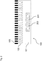
- Fig. 1 shows a schematic representation of a connection adapter 100 according to one embodiment.
- the connection adapter 100 comprises a printed circuit board 101 with twenty comb teeth 103, each having an electrical contact surface 105, an electrical connector interface 107, which has twenty electrical connections 109, two openings 111, by means of which a connector can be positively or positively connected to the circuit board 101 , a labeling field 113, a marking field 115 and three bores 117.
- connection adapter 100 for a terminal arrangement may be formed with: the circuit board 101 having a comb-shaped line structure with the number of comb teeth 103, the comb teeth 103 each having an electrical contact surface 105; the electrical connector interface 107 for a connector, wherein the electrical connector interface 107 electrical connections 109 which are electrically connected to the electrical contact surfaces 105 of the comb teeth 103, and wherein the electrical connector interface 107 is disposed on the circuit board 101.
- the terminal arrangement may be a terminal block arrangement, in particular a terminal block arrangement arranged in a control cabinet.
- the numbers may be 1, 2, 3, 4, 5, 6, 7, 8, 9, 10, 15, 20, 25, 30, 35, 40, 45 or 50. According to one embodiment, the number may be a number corresponding to the connector used or any number of poles.
- the electrical connection terminals can be formed by screw terminals. In this case, by screwing the screw terminals further a mechanical fixation of the connection adapter 100 can be achieved at the terminal assembly.
- the comb-shaped line structure may be formed by conductor tracks on the printed circuit board 101.
- the electrical contact surfaces 105 may each be formed by a copper layer.
- the comb teeth 103 are each coated on one side, on two sides or on all sides with copper.
- the electrical connector interface 107 may have an interface for connection to a FLK connector, an HD variant of an FLK connector, a D-sub connector, an HD variant of a D-sub connector, an ELCO connector, a Fujitsu FCN Connectors, an IEC 60603 connector, a PxC Mini-Combicon family connector, the PxC Combicon family or the PxC Power-Combicon family, and / or any other PxC connector.
- the printed circuit board 101 may be a FR4 printed circuit board.
- a terminal assembly for contacting a control side of a terminal assembly, such as a terminal, different, for example, the grid of the terminal assembly adapted, as universal and / or specially designed printed circuit boards 101 for different numbers of poles, in particular system cable dependent, are used.
- This can be a faster and easier way non-interchangeable connection of an electrical device, such as a controller, are made possible to the terminal assembly.
- the comb teeth 103 of the printed circuit board 101 can be made somewhat narrower than the terminal spaces of the electrical connection terminals in order to be able to compensate for small deviations in the grid of the terminal arrangement.
- the electrical connection terminals can each comprise a clamping body which can be pressed against a comb tooth 103 to fix the comb teeth 103 mechanically to the electrical connection terminal and to electrically contact the electrical connection surface 105 of the comb teeth 103, for example via a clamping surface ,
- the clamping body is made of galvanized steel.
- connection adapters 100 may be connected to the terminal assembly.
- the connection adapters 100 of the plurality of connection adapters 100 can be made in various adaptations, such as variants, to facilitate connection to the terminal arrangement. This can be advantageous in particular in the case of a multi-level terminal arrangement.
- the comb teeth 105 can be staggered to allow access with a tool, such as a screwdriver, to a plane of a multi-level terminal assembly.
- the various adaptations of the connection adapter 100 may be referred to as left, right, top, center, bottom, and all combinations resulting therefrom.
- the associated designation such as a terminal block designation
- the labeling field 113 on the printed circuit board 101.
- a mark for left and right adaptation for example by means of different colors, can be applied.
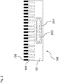
- connection adapter 100 comprises the circuit board 101 with twenty comb teeth 103, each having an electrical contact surface 105, and a connector 201 which includes twenty electrical terminals 203 and is connected to the non-illustrated electrical connector interface 107.
- the connector 201 may be formed as a FLK connector or as a system connector. Further, a width of the comb teeth 103 2mm and a distance of two adjacent comb teeth 103 may be 3mm. A length of the comb teeth 103 may further be 18mm. A width of the circuit board 101 may further be 105mm. Further, a height of the circuit board 101 without the comb teeth 103 may be 20mm.
- a pitch of the comb teeth may be selected depending on the terminal blocks to be adapted.
- the pitch can be performed at all conceivable intervals, in particular with a minimum tine width of 1mm and / or a minimum distance between adjacent tines of 1mm, and tine widths.
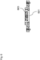
- Fig. 3 shows a schematic representation of the connection adapter 100 according to another embodiment.
- the Indian Fig. 3 illustrated connection adapter 100 differs from that in the Fig. 2 illustrated connection adapter 100 only by the height of the circuit board 101 without the comb teeth 103. This can in the in the Fig. 3 shown connection adapter 100 15mm.
- Fig. 4 shows a perspective view of the connection adapter 100 according to another embodiment.
- the connection adapter 100 comprises the circuit board 101 with twenty comb teeth 103, each having an electrical contact surface 105, and the connector 201. Further, the circuit board 101, two holes 117 and a plurality of holes 401 on. For example, can be realized by a position of the circuit board 101 by means of the holes 401 a through hole for not shown interconnects.
- connection assembly 500 comprises twenty terminal blocks 501 arranged in series, each having an electrical connection terminal 503 on both sides.
- the comb teeth 103 of the connection adapter 100 are inserted into the electrical terminals 501.
- Fig. 6 shows a plan view of a two-storey terminal block 601.
- the two-storey terminal 601 is formed as a screw terminal and comprises four screws 603. By tightening the screws 603 can be inserted into the associated unillustrated electrical terminal 503 unimagined comb teeth 103 with the electrical terminal 503 mechanically fixed and the electrical contact surface 105 of the comb tooth 103 are electrically connected to the electrical terminal 503.
- connection assembly 500 comprises twenty two-tier terminal blocks 601, each having two electrical terminals 503 on both sides.
- the comb teeth 103 of the connection adapters 100 are inserted into the electrical terminals 503.
- Figs. 8 to 10 show various embodiments of an electrical contact surface 105 of a comb-tooth 103.
- Fig. 8A shows a side view of a comb tooth 103
- the electrical contact surface 105 is formed by a full-surface four-sided copper coating of the comb tooth 103.
- a thickness of the copper coating may be 35 ⁇ m to 105 ⁇ m.
- a thickness of the comb tooth 103 may be 1.5 mm or more.
- Fig. 8B shows a view of the in Fig. 8A pictured comb teeth 103.
- Fig. 9A shows a side view of a comb-tooth 103 with a plurality of electrical contact surfaces 105, which is arranged on an upper side and a lower side of the comb-tooth 103.
- the plurality of electrical contact surfaces 105 may be formed by a copper coating having a thickness of 35 ⁇ m to 105 ⁇ m. Further, a thickness of the comb tooth 103 may be 1.5 mm or more.
- Fig. 9B shows a view of the in Fig. 9A illustrated comb teeth 103.
- the electrical contact surfaces 105 of the plurality of electrical contact surfaces 105 are connected by means of electrically conductive webs 901 and have different geometric shapes.
- the geometric shapes are square shapes, circular shapes, triangular shapes and pentagonal shapes. By choosing the geometric shapes, a contacting of the electrical connection terminal 503 can be optimized, in particular in the case of corrosion or in the case of the formation of oxide layers.
- Fig. 10A shows a side view of a comb tooth 103
- the electrical contact surface 105 is formed by a two-sided copper coating of the comb tooth 103.
- a thickness of the copper coating may be 35 ⁇ m to 105 ⁇ m.
- a thickness of the Comb teeth 103 1.5mm or more.
- Fig. 10B shows a view of the in Fig. 10A illustrated comb teeth 103.
- the electrical contact surface 105 may extend over the entire width of the comb tooth 103.
- the electrical contact surface 105 extends to the edges of the comb tooth 103.
- Fig. 11A shows a plan view of the circuit board 101 according to one embodiment.
- the printed circuit board 101 has ten comb teeth 103, each having an electrical contact surface 105, an electrical signal transmission interface 1101 with ten electrical connections 1103 and six openings 1105 for attaching a spacer bolt.
- the connector 201 is arranged with twenty electrical terminals 203 on the circuit board 101.
- the electrical connections 1103 may be formed by plated-through holes of the printed circuit board 101.
- the circuit board 101 may further comprise 2, 4, 6, 8 or 10 openings 1105, which may be formed by bores.
- connection adapter 100 may be formed with the electrical signal transmission interface 1101, in particular an electrical signal transmission interface 1101 formed in or on the circuit board 101, wherein the electrical signal transmission interface 1101 is electrically connected to the electrical connector interface 107.
- Fig. 11B shows a plan view of another circuit board 1107 according to one embodiment.
- the further circuit board 1107 has ten comb teeth 1109, which each have an electrical contact surface 1111, an electrical signal transmission interface 1113 with ten electrical connections 1115 and six openings 1105 for fastening a spacer bolt.
- the electrical connections 1115 may be formed by plated-through holes of the further printed circuit board 1107.
- the further circuit board 1107 may further comprise 2, 4, 6, 8 or 10 openings 1105, which may be formed by bores.
- connection adapter 100 may be formed with: the further circuit board 1107 having a comb-shaped line structure with a plurality of comb teeth 1109, the comb teeth 1109 each having an electrical contact surface 1111; and another electrical signal transmission interface 1113, in particular a further electrical signal transmission interface 1113 formed in or on the further printed circuit board 1107, the further signal transmission interface 1113 being electrically connected to the electrical signal transmission interface 1101 of the printed circuit board 101 and to the electrical contact surfaces 1111 of the comb teeth 1109 of the further printed circuit board 1107.
- the electrical connections 1103 may be electrically connected to the electrical connections 1115 by means of a connecting line, in particular by means of a solderable cable connection of different numbers of poles, or a sandwich strip.
- the electrical connections 203 of the connector 201 arranged on the printed circuit board 101 can be electrically connected to the electrical contact surfaces 1111 of the further printed circuit board 1107.
- the upper row of electrical terminals 203 which may include a pin 1
- the lower row of electrical terminals 203 which may include a pin 2
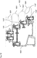
- Fig. 12 shows a cross-sectional view of an arrangement with a plurality of double-tiered terminal blocks 601 and the connection adapter 100 according to another embodiment.
- the connection adapter 100 comprises the printed circuit board 101 with the electrical signal transmission interface 1101 (not shown), the further printed circuit board 1107 with the further electrical signal transmission interface 1113, a sandwich strip 1201, which electrically connects the electrical signal transmission interface 1101 and the further electrical signal transmission interface 1113, and spacer bolts 1203, which mechanically connect the circuit board 101 with the other circuit board 1107. Furthermore, dimensions and dimensions are shown in the unit millimeters.
- the sandwich strip 1201 may comprise a plurality of contact pins. Furthermore, the contact pins of the sandwich strip 1201 can be soldered to the unillustrated electrical connections 1103, 1115. Furthermore, the spacer bolts 1203 may be plastic bolts. The spacer bolts 1203 may further be bolted to the circuit board 101 and the other circuit board 1107, respectively. For example, screws are guided through the openings 1105, not shown.
- Fig. 13 shows a perspective view of the in Fig. 12 shown arrangement.
- the terminal assembly 500 is formed by an array of two-tiered terminal blocks 601. Further shows Fig. 14 a perspective view of in Fig. 12 shown arrangement with another connection adapter 100th
- Fig. 15 shows a schematic representation of the connection adapter 100 according to another embodiment.
- the connection adapter 100 comprises the circuit board 101, the further circuit board 1107 and a flexible circuit board section 1501, which connects the circuit board 101 and the further circuit board 1107 mechanically and electrically.
- the printed circuit board 101 also has comb teeth 103 with electrical contact surfaces 105.
- the connector 201 is disposed on the circuit board 101.
- the further printed circuit board 1107 also has comb teeth 1109 with electrical contact surfaces 1111.
- the flexible printed circuit board component 1501 conductor tracks.
- a compensation of lateral offset and / or height differences of individual levels of a multi-level terminal arrangement 500 can be made possible.
- Fig. 16 shows a cross-sectional view of an arrangement with the in Fig. 6 shown double-tiered terminal 601 and the connection adapter 100 according to the in Fig. 15 shown embodiment.
- the connection adapter 100 includes the circuit board 101 on which the connector 201 is disposed, the flexible board portion 1501, and the other board 1107.
- the connection adapter 100 is connected to the two-level terminal 601.
- Fig. 17 shows a cross-sectional view of an arrangement with a three-tier terminal 1701 and the connection adapter 100 according to another embodiment.
- the connection adapter 100 includes the circuit board 101 on which the connector 201 is disposed, two flexible circuit board parts 1501, and two other circuit boards 1107. Further, the connection adapter 100 is connected to the three-level terminal block 1701.
- two flexible board portions 1501 may be mechanically and electrically connected to another board 1107.
- a flexible printed circuit board component 1501 from above and a flexible printed circuit board component 1501 from below are laminated to the further printed circuit board 1107.
- Fig. 18 shows a cross-sectional view of an arrangement with a four-tiered terminal 1801 and the connection adapter 100 according to another embodiment.
- the connection adapter 100 includes the circuit board 101 on which the connector 201 is disposed, three flexible circuit board parts 1501, and three other circuit boards 1107. Further, the connection adapter 100 is connected to the four-level terminal block 1701.
Landscapes
- Engineering & Computer Science (AREA)
- Microelectronics & Electronic Packaging (AREA)
- Coupling Device And Connection With Printed Circuit (AREA)
Priority Applications (1)
| Application Number | Priority Date | Filing Date | Title |
|---|---|---|---|
| PL15790997T PL3227975T3 (pl) | 2014-12-04 | 2015-11-09 | Adapter przyłączeniowy dla układu zacisków przyłączeniowych |
Applications Claiming Priority (2)
| Application Number | Priority Date | Filing Date | Title |
|---|---|---|---|
| DE102014117868.8A DE102014117868A1 (de) | 2014-12-04 | 2014-12-04 | Verbindungsadapter für eine Anschlussklemmenanordnung |
| PCT/EP2015/076092 WO2016087164A1 (de) | 2014-12-04 | 2015-11-09 | Verbindungsadapter für eine anschlussklemmenanordnung |
Publications (2)
| Publication Number | Publication Date |
|---|---|
| EP3227975A1 EP3227975A1 (de) | 2017-10-11 |
| EP3227975B1 true EP3227975B1 (de) | 2019-04-10 |
Family
ID=54476998
Family Applications (1)
| Application Number | Title | Priority Date | Filing Date |
|---|---|---|---|
| EP15790997.9A Active EP3227975B1 (de) | 2014-12-04 | 2015-11-09 | Verbindungsadapter für eine anschlussklemmenanordnung |
Country Status (6)
| Country | Link |
|---|---|
| US (1) | US10193287B2 (pl) |
| EP (1) | EP3227975B1 (pl) |
| CN (1) | CN107112655B (pl) |
| DE (1) | DE102014117868A1 (pl) |
| PL (1) | PL3227975T3 (pl) |
| WO (1) | WO2016087164A1 (pl) |
Cited By (1)
| Publication number | Priority date | Publication date | Assignee | Title |
|---|---|---|---|---|
| US20250183605A1 (en) * | 2023-12-04 | 2025-06-05 | Channel Well Technology Co., Ltd. | Multifunctional charging and data adapter |
Families Citing this family (5)
| Publication number | Priority date | Publication date | Assignee | Title |
|---|---|---|---|---|
| DE102015120788A1 (de) | 2015-11-30 | 2017-06-01 | Phoenix Contact Gmbh & Co. Kg | Schleifenbrücke |
| DE102016122263A1 (de) * | 2016-11-18 | 2018-05-24 | Phoenix Contact Gmbh & Co. Kg | Rangierverbinder und Verfahren zum Herstellen eines Rangierverbinders |
| CN108539479A (zh) * | 2018-05-11 | 2018-09-14 | 系新电子技术(苏州)有限公司 | 一种组合式线缆连接装置 |
| CN109618491A (zh) * | 2018-12-29 | 2019-04-12 | 联想(北京)有限公司 | 一种电路板 |
| US11749922B2 (en) * | 2020-09-01 | 2023-09-05 | Ge Infrastructure Technology Llc | Dual-sided connector for printed circuit board |
Family Cites Families (13)
| Publication number | Priority date | Publication date | Assignee | Title |
|---|---|---|---|---|
| JPS50145462U (pl) * | 1974-05-20 | 1975-12-02 | ||
| GB2035716A (en) * | 1978-08-09 | 1980-06-18 | Westinghouse Brake & Signal | Improvements relating to electrical signal connectors |
| US4936785A (en) * | 1988-12-19 | 1990-06-26 | Krug Eric M | Interchangeable adapter module for electronic devices |
| DE4438804C1 (de) * | 1994-10-31 | 1996-03-28 | Weidmueller Interface | Modulare Steuerungsanlage mit Busleiter z. B. zur Gebäudeautomatisierung |
| SE507939C2 (sv) * | 1996-04-23 | 1998-08-03 | Asea Brown Boveri | Anordning för överföring av elektriska signaler |
| US6004139A (en) * | 1997-06-24 | 1999-12-21 | International Business Machines Corporation | Memory module interface card adapter |
| US6261104B1 (en) * | 1999-08-16 | 2001-07-17 | Micron Electronics, Inc. | Riser card assembly and method for its installation |
| DE10148470A1 (de) * | 2001-10-01 | 2003-04-17 | Siemens Ag | Vorrichtung und Verfahren zum elektrischen und mechanischen Verbinden von Komponenten eines Automatisierungssystems |
| DE10251615A1 (de) * | 2002-11-06 | 2004-05-19 | Valeo Schalter Und Sensoren Gmbh | Steckerelement und Platinenaufbau |
| DE102006025604A1 (de) * | 2006-05-24 | 2007-11-29 | Friedrich Lütze Gmbh & Co. Kg | Vorrichtung zum selbsttätigen Abschalten oder Schalten eines elektrischen Verbrauchers |
| DE202007011112U1 (de) * | 2007-08-09 | 2007-11-15 | Mc Technology Gmbh | Adapterplatte, Steckfassung und Vorrichtung zur Verbindung einer elektronischen Steuerung mit ihren Anschlussleitungen |
| US8113864B2 (en) * | 2010-05-13 | 2012-02-14 | Delta Electronics, Inc. | Quick-detachable terminal seat and programmable logic controller having the same |
| KR101735474B1 (ko) | 2010-08-23 | 2017-05-16 | 삼성전자주식회사 | 인쇄회로기판 조립체의 몰딩방법 |
-
2014
- 2014-12-04 DE DE102014117868.8A patent/DE102014117868A1/de not_active Withdrawn
-
2015
- 2015-11-09 US US15/532,023 patent/US10193287B2/en active Active
- 2015-11-09 CN CN201580065941.6A patent/CN107112655B/zh not_active Expired - Fee Related
- 2015-11-09 WO PCT/EP2015/076092 patent/WO2016087164A1/de not_active Ceased
- 2015-11-09 EP EP15790997.9A patent/EP3227975B1/de active Active
- 2015-11-09 PL PL15790997T patent/PL3227975T3/pl unknown
Non-Patent Citations (1)
| Title |
|---|
| None * |
Cited By (1)
| Publication number | Priority date | Publication date | Assignee | Title |
|---|---|---|---|---|
| US20250183605A1 (en) * | 2023-12-04 | 2025-06-05 | Channel Well Technology Co., Ltd. | Multifunctional charging and data adapter |
Also Published As
| Publication number | Publication date |
|---|---|
| DE102014117868A1 (de) | 2016-06-09 |
| US20170271830A1 (en) | 2017-09-21 |
| EP3227975A1 (de) | 2017-10-11 |
| US10193287B2 (en) | 2019-01-29 |
| CN107112655B (zh) | 2019-10-11 |
| WO2016087164A1 (de) | 2016-06-09 |
| CN107112655A (zh) | 2017-08-29 |
| PL3227975T3 (pl) | 2019-08-30 |
Similar Documents
| Publication | Publication Date | Title |
|---|---|---|
| EP3227975B1 (de) | Verbindungsadapter für eine anschlussklemmenanordnung | |
| EP1758206B1 (de) | Vertikale Steckmöglichkeit bei Reihenklemme mit Etagenversatz | |
| DE69719025T2 (de) | Ansteckbare elektrische anschlussleiste | |
| EP2236330A1 (de) | Elektrische Heizvorrichtung für ein Kraftfahrzeug | |
| DE112019004328T5 (de) | Lötfreie Verbindung zu Hochfrequenzlitze | |
| EP1239544B1 (de) | Elektrisches Gerät mit Busleiterabschnitt | |
| EP2111088A2 (de) | Modulare Montagebasis für elektrische Geräte | |
| EP3553898A1 (de) | Stromführungsprofil und abgriffsteckverbinder | |
| DE102017116342A1 (de) | Leiterplattenanordnung mit einer Kontaktvorrichtung zur leitenden Verbindung der Leiterplatten der Leiterplattenanordnung nach Art eines Bussystems | |
| DE102008025433A1 (de) | Klemmenanschlußblock | |
| EP2120296A1 (de) | Anreihbares Elektronikgehäuse mit einer Anschlußleiste | |
| DE102017117300A1 (de) | Querbrücker und Reihenklemmenanordnung | |
| DE102009016160B4 (de) | Verfahren zur Herstellung einer Kontaktvorrichtung und Kontaktvorrichtung | |
| DE102015115819A1 (de) | Leiterbrückenelement sowie Bestückungsgurt und Leiterplatten mit einem solchen | |
| EP3874919B1 (de) | Gehäuse für einen switch für bahnanwendungen | |
| EP3503312A1 (de) | Stromführungsprofil | |
| DE60301460T2 (de) | Anordnung für die elektrische Verbindung eines Bauteils auf der Oberfläche einer Leiterplatte | |
| DE202018100964U1 (de) | Kontakt- und Busschienenanordnung | |
| EP2673847B1 (de) | Direktsteckverbinder zur elektrischen direktkontaktierung einer leiterplatte | |
| EP1623484B1 (de) | Kontaktleiste zur elektrischen kontaktierung von beidseitig auf einer leiterplatte verlaufenden metallischen leiterbahnen | |
| LU500973B1 (de) | Steckeinrichtung und Bausatz mit einer Steckeinrichtung | |
| WO2015124482A1 (de) | Steckeranschlusselement, verbindungsanordnung mit mehreren steckeranschlusselementen in einem elektrischen gerät und einpresswerkzeug zur ausbildung einer verbindungsanordnung | |
| DE2139701B2 (de) | Elektronische Anlage mit einem Rahmen zur Aufnahme von steckbaren Karten mit gedruckten Schaltungen | |
| DE102018118976A1 (de) | Vorrichtung zur Übertragung von elektrischen Signalen oder von elektrischem Strom, eine elektrische Baugruppe sowie ein Baukasten | |
| EP1083434A2 (de) | Vorrichtung zum Prüfen von Leiterplatten |
Legal Events
| Date | Code | Title | Description |
|---|---|---|---|
| STAA | Information on the status of an ep patent application or granted ep patent |
Free format text: STATUS: THE INTERNATIONAL PUBLICATION HAS BEEN MADE |
|
| PUAI | Public reference made under article 153(3) epc to a published international application that has entered the european phase |
Free format text: ORIGINAL CODE: 0009012 |
|
| STAA | Information on the status of an ep patent application or granted ep patent |
Free format text: STATUS: REQUEST FOR EXAMINATION WAS MADE |
|
| 17P | Request for examination filed |
Effective date: 20170518 |
|
| AK | Designated contracting states |
Kind code of ref document: A1 Designated state(s): AL AT BE BG CH CY CZ DE DK EE ES FI FR GB GR HR HU IE IS IT LI LT LU LV MC MK MT NL NO PL PT RO RS SE SI SK SM TR |
|
| AX | Request for extension of the european patent |
Extension state: BA ME |
|
| DAV | Request for validation of the european patent (deleted) | ||
| DAX | Request for extension of the european patent (deleted) | ||
| GRAP | Despatch of communication of intention to grant a patent |
Free format text: ORIGINAL CODE: EPIDOSNIGR1 |
|
| STAA | Information on the status of an ep patent application or granted ep patent |
Free format text: STATUS: GRANT OF PATENT IS INTENDED |
|
| INTG | Intention to grant announced |
Effective date: 20181120 |
|
| GRAS | Grant fee paid |
Free format text: ORIGINAL CODE: EPIDOSNIGR3 |
|
| GRAA | (expected) grant |
Free format text: ORIGINAL CODE: 0009210 |
|
| STAA | Information on the status of an ep patent application or granted ep patent |
Free format text: STATUS: THE PATENT HAS BEEN GRANTED |
|
| AK | Designated contracting states |
Kind code of ref document: B1 Designated state(s): AL AT BE BG CH CY CZ DE DK EE ES FI FR GB GR HR HU IE IS IT LI LT LU LV MC MK MT NL NO PL PT RO RS SE SI SK SM TR |
|
| REG | Reference to a national code |
Ref country code: GB Ref legal event code: FG4D Free format text: NOT ENGLISH |
|
| REG | Reference to a national code |
Ref country code: CH Ref legal event code: EP Ref country code: AT Ref legal event code: REF Ref document number: 1119963 Country of ref document: AT Kind code of ref document: T Effective date: 20190415 |
|
| REG | Reference to a national code |
Ref country code: IE Ref legal event code: FG4D Free format text: LANGUAGE OF EP DOCUMENT: GERMAN |
|
| REG | Reference to a national code |
Ref country code: DE Ref legal event code: R096 Ref document number: 502015008674 Country of ref document: DE |
|
| REG | Reference to a national code |
Ref country code: NL Ref legal event code: MP Effective date: 20190410 |
|
| REG | Reference to a national code |
Ref country code: LT Ref legal event code: MG4D |
|
| PG25 | Lapsed in a contracting state [announced via postgrant information from national office to epo] |
Ref country code: NL Free format text: LAPSE BECAUSE OF FAILURE TO SUBMIT A TRANSLATION OF THE DESCRIPTION OR TO PAY THE FEE WITHIN THE PRESCRIBED TIME-LIMIT Effective date: 20190410 |
|
| PG25 | Lapsed in a contracting state [announced via postgrant information from national office to epo] |
Ref country code: FI Free format text: LAPSE BECAUSE OF FAILURE TO SUBMIT A TRANSLATION OF THE DESCRIPTION OR TO PAY THE FEE WITHIN THE PRESCRIBED TIME-LIMIT Effective date: 20190410 Ref country code: SE Free format text: LAPSE BECAUSE OF FAILURE TO SUBMIT A TRANSLATION OF THE DESCRIPTION OR TO PAY THE FEE WITHIN THE PRESCRIBED TIME-LIMIT Effective date: 20190410 Ref country code: ES Free format text: LAPSE BECAUSE OF FAILURE TO SUBMIT A TRANSLATION OF THE DESCRIPTION OR TO PAY THE FEE WITHIN THE PRESCRIBED TIME-LIMIT Effective date: 20190410 Ref country code: HR Free format text: LAPSE BECAUSE OF FAILURE TO SUBMIT A TRANSLATION OF THE DESCRIPTION OR TO PAY THE FEE WITHIN THE PRESCRIBED TIME-LIMIT Effective date: 20190410 Ref country code: LT Free format text: LAPSE BECAUSE OF FAILURE TO SUBMIT A TRANSLATION OF THE DESCRIPTION OR TO PAY THE FEE WITHIN THE PRESCRIBED TIME-LIMIT Effective date: 20190410 Ref country code: AL Free format text: LAPSE BECAUSE OF FAILURE TO SUBMIT A TRANSLATION OF THE DESCRIPTION OR TO PAY THE FEE WITHIN THE PRESCRIBED TIME-LIMIT Effective date: 20190410 Ref country code: NO Free format text: LAPSE BECAUSE OF FAILURE TO SUBMIT A TRANSLATION OF THE DESCRIPTION OR TO PAY THE FEE WITHIN THE PRESCRIBED TIME-LIMIT Effective date: 20190710 Ref country code: PT Free format text: LAPSE BECAUSE OF FAILURE TO SUBMIT A TRANSLATION OF THE DESCRIPTION OR TO PAY THE FEE WITHIN THE PRESCRIBED TIME-LIMIT Effective date: 20190910 |
|
| PG25 | Lapsed in a contracting state [announced via postgrant information from national office to epo] |
Ref country code: LV Free format text: LAPSE BECAUSE OF FAILURE TO SUBMIT A TRANSLATION OF THE DESCRIPTION OR TO PAY THE FEE WITHIN THE PRESCRIBED TIME-LIMIT Effective date: 20190410 Ref country code: GR Free format text: LAPSE BECAUSE OF FAILURE TO SUBMIT A TRANSLATION OF THE DESCRIPTION OR TO PAY THE FEE WITHIN THE PRESCRIBED TIME-LIMIT Effective date: 20190711 Ref country code: RS Free format text: LAPSE BECAUSE OF FAILURE TO SUBMIT A TRANSLATION OF THE DESCRIPTION OR TO PAY THE FEE WITHIN THE PRESCRIBED TIME-LIMIT Effective date: 20190410 Ref country code: BG Free format text: LAPSE BECAUSE OF FAILURE TO SUBMIT A TRANSLATION OF THE DESCRIPTION OR TO PAY THE FEE WITHIN THE PRESCRIBED TIME-LIMIT Effective date: 20190710 |
|
| PG25 | Lapsed in a contracting state [announced via postgrant information from national office to epo] |
Ref country code: IS Free format text: LAPSE BECAUSE OF FAILURE TO SUBMIT A TRANSLATION OF THE DESCRIPTION OR TO PAY THE FEE WITHIN THE PRESCRIBED TIME-LIMIT Effective date: 20190810 |
|
| REG | Reference to a national code |
Ref country code: DE Ref legal event code: R097 Ref document number: 502015008674 Country of ref document: DE |
|
| PG25 | Lapsed in a contracting state [announced via postgrant information from national office to epo] |
Ref country code: RO Free format text: LAPSE BECAUSE OF FAILURE TO SUBMIT A TRANSLATION OF THE DESCRIPTION OR TO PAY THE FEE WITHIN THE PRESCRIBED TIME-LIMIT Effective date: 20190410 Ref country code: CZ Free format text: LAPSE BECAUSE OF FAILURE TO SUBMIT A TRANSLATION OF THE DESCRIPTION OR TO PAY THE FEE WITHIN THE PRESCRIBED TIME-LIMIT Effective date: 20190410 Ref country code: EE Free format text: LAPSE BECAUSE OF FAILURE TO SUBMIT A TRANSLATION OF THE DESCRIPTION OR TO PAY THE FEE WITHIN THE PRESCRIBED TIME-LIMIT Effective date: 20190410 Ref country code: SK Free format text: LAPSE BECAUSE OF FAILURE TO SUBMIT A TRANSLATION OF THE DESCRIPTION OR TO PAY THE FEE WITHIN THE PRESCRIBED TIME-LIMIT Effective date: 20190410 Ref country code: DK Free format text: LAPSE BECAUSE OF FAILURE TO SUBMIT A TRANSLATION OF THE DESCRIPTION OR TO PAY THE FEE WITHIN THE PRESCRIBED TIME-LIMIT Effective date: 20190410 |
|
| PLBE | No opposition filed within time limit |
Free format text: ORIGINAL CODE: 0009261 |
|
| STAA | Information on the status of an ep patent application or granted ep patent |
Free format text: STATUS: NO OPPOSITION FILED WITHIN TIME LIMIT |
|
| PG25 | Lapsed in a contracting state [announced via postgrant information from national office to epo] |
Ref country code: SM Free format text: LAPSE BECAUSE OF FAILURE TO SUBMIT A TRANSLATION OF THE DESCRIPTION OR TO PAY THE FEE WITHIN THE PRESCRIBED TIME-LIMIT Effective date: 20190410 |
|
| 26N | No opposition filed |
Effective date: 20200113 |
|
| PG25 | Lapsed in a contracting state [announced via postgrant information from national office to epo] |
Ref country code: TR Free format text: LAPSE BECAUSE OF FAILURE TO SUBMIT A TRANSLATION OF THE DESCRIPTION OR TO PAY THE FEE WITHIN THE PRESCRIBED TIME-LIMIT Effective date: 20190410 |
|
| PG25 | Lapsed in a contracting state [announced via postgrant information from national office to epo] |
Ref country code: SI Free format text: LAPSE BECAUSE OF FAILURE TO SUBMIT A TRANSLATION OF THE DESCRIPTION OR TO PAY THE FEE WITHIN THE PRESCRIBED TIME-LIMIT Effective date: 20190410 |
|
| REG | Reference to a national code |
Ref country code: CH Ref legal event code: PL |
|
| PG25 | Lapsed in a contracting state [announced via postgrant information from national office to epo] |
Ref country code: LU Free format text: LAPSE BECAUSE OF NON-PAYMENT OF DUE FEES Effective date: 20191109 Ref country code: LI Free format text: LAPSE BECAUSE OF NON-PAYMENT OF DUE FEES Effective date: 20191130 Ref country code: MC Free format text: LAPSE BECAUSE OF FAILURE TO SUBMIT A TRANSLATION OF THE DESCRIPTION OR TO PAY THE FEE WITHIN THE PRESCRIBED TIME-LIMIT Effective date: 20190410 Ref country code: CH Free format text: LAPSE BECAUSE OF NON-PAYMENT OF DUE FEES Effective date: 20191130 |
|
| REG | Reference to a national code |
Ref country code: BE Ref legal event code: MM Effective date: 20191130 |
|
| GBPC | Gb: european patent ceased through non-payment of renewal fee |
Effective date: 20191109 |
|
| PG25 | Lapsed in a contracting state [announced via postgrant information from national office to epo] |
Ref country code: IE Free format text: LAPSE BECAUSE OF NON-PAYMENT OF DUE FEES Effective date: 20191109 Ref country code: GB Free format text: LAPSE BECAUSE OF NON-PAYMENT OF DUE FEES Effective date: 20191109 Ref country code: FR Free format text: LAPSE BECAUSE OF NON-PAYMENT OF DUE FEES Effective date: 20191130 |
|
| PG25 | Lapsed in a contracting state [announced via postgrant information from national office to epo] |
Ref country code: BE Free format text: LAPSE BECAUSE OF NON-PAYMENT OF DUE FEES Effective date: 20191130 |
|
| PG25 | Lapsed in a contracting state [announced via postgrant information from national office to epo] |
Ref country code: CY Free format text: LAPSE BECAUSE OF FAILURE TO SUBMIT A TRANSLATION OF THE DESCRIPTION OR TO PAY THE FEE WITHIN THE PRESCRIBED TIME-LIMIT Effective date: 20190410 |
|
| PG25 | Lapsed in a contracting state [announced via postgrant information from national office to epo] |
Ref country code: HU Free format text: LAPSE BECAUSE OF FAILURE TO SUBMIT A TRANSLATION OF THE DESCRIPTION OR TO PAY THE FEE WITHIN THE PRESCRIBED TIME-LIMIT; INVALID AB INITIO Effective date: 20151109 Ref country code: MT Free format text: LAPSE BECAUSE OF FAILURE TO SUBMIT A TRANSLATION OF THE DESCRIPTION OR TO PAY THE FEE WITHIN THE PRESCRIBED TIME-LIMIT Effective date: 20190410 |
|
| REG | Reference to a national code |
Ref country code: AT Ref legal event code: MM01 Ref document number: 1119963 Country of ref document: AT Kind code of ref document: T Effective date: 20201109 |
|
| PG25 | Lapsed in a contracting state [announced via postgrant information from national office to epo] |
Ref country code: AT Free format text: LAPSE BECAUSE OF NON-PAYMENT OF DUE FEES Effective date: 20201109 |
|
| PG25 | Lapsed in a contracting state [announced via postgrant information from national office to epo] |
Ref country code: MK Free format text: LAPSE BECAUSE OF FAILURE TO SUBMIT A TRANSLATION OF THE DESCRIPTION OR TO PAY THE FEE WITHIN THE PRESCRIBED TIME-LIMIT Effective date: 20190410 |
|
| PGFP | Annual fee paid to national office [announced via postgrant information from national office to epo] |
Ref country code: PL Payment date: 20221028 Year of fee payment: 8 |
|
| P01 | Opt-out of the competence of the unified patent court (upc) registered |
Effective date: 20230424 |
|
| PGFP | Annual fee paid to national office [announced via postgrant information from national office to epo] |
Ref country code: IT Payment date: 20231124 Year of fee payment: 9 |
|
| PGFP | Annual fee paid to national office [announced via postgrant information from national office to epo] |
Ref country code: DE Payment date: 20250129 Year of fee payment: 10 |
|
| PG25 | Lapsed in a contracting state [announced via postgrant information from national office to epo] |
Ref country code: PL Free format text: LAPSE BECAUSE OF NON-PAYMENT OF DUE FEES Effective date: 20231109 |
|
| PG25 | Lapsed in a contracting state [announced via postgrant information from national office to epo] |
Ref country code: IT Free format text: LAPSE BECAUSE OF NON-PAYMENT OF DUE FEES Effective date: 20241109 |