EP3213036B1 - Magnetfeldsensor mit kalibrierungsschaltung und -techniken - Google Patents
Magnetfeldsensor mit kalibrierungsschaltung und -techniken Download PDFInfo
- Publication number
- EP3213036B1 EP3213036B1 EP15791840.0A EP15791840A EP3213036B1 EP 3213036 B1 EP3213036 B1 EP 3213036B1 EP 15791840 A EP15791840 A EP 15791840A EP 3213036 B1 EP3213036 B1 EP 3213036B1
- Authority
- EP
- European Patent Office
- Prior art keywords
- magnetic field
- signal
- field signal
- digital
- circuit
- Prior art date
- Legal status (The legal status is an assumption and is not a legal conclusion. Google has not performed a legal analysis and makes no representation as to the accuracy of the status listed.)
- Active
Links
Images






Classifications
-
- G—PHYSICS
- G01—MEASURING; TESTING
- G01R—MEASURING ELECTRIC VARIABLES; MEASURING MAGNETIC VARIABLES
- G01R35/00—Testing or calibrating of apparatus covered by the other groups of this subclass
- G01R35/005—Calibrating; Standards or reference devices, e.g. voltage or resistance standards, "golden" references
-
- G—PHYSICS
- G01—MEASURING; TESTING
- G01D—MEASURING NOT SPECIALLY ADAPTED FOR A SPECIFIC VARIABLE; ARRANGEMENTS FOR MEASURING TWO OR MORE VARIABLES NOT COVERED IN A SINGLE OTHER SUBCLASS; TARIFF METERING APPARATUS; MEASURING OR TESTING NOT OTHERWISE PROVIDED FOR
- G01D5/00—Mechanical means for transferring the output of a sensing member; Means for converting the output of a sensing member to another variable where the form or nature of the sensing member does not constrain the means for converting; Transducers not specially adapted for a specific variable
- G01D5/12—Mechanical means for transferring the output of a sensing member; Means for converting the output of a sensing member to another variable where the form or nature of the sensing member does not constrain the means for converting; Transducers not specially adapted for a specific variable using electric or magnetic means
- G01D5/14—Mechanical means for transferring the output of a sensing member; Means for converting the output of a sensing member to another variable where the form or nature of the sensing member does not constrain the means for converting; Transducers not specially adapted for a specific variable using electric or magnetic means influencing the magnitude of a current or voltage
- G01D5/142—Mechanical means for transferring the output of a sensing member; Means for converting the output of a sensing member to another variable where the form or nature of the sensing member does not constrain the means for converting; Transducers not specially adapted for a specific variable using electric or magnetic means influencing the magnitude of a current or voltage using Hall-effect devices
- G01D5/145—Mechanical means for transferring the output of a sensing member; Means for converting the output of a sensing member to another variable where the form or nature of the sensing member does not constrain the means for converting; Transducers not specially adapted for a specific variable using electric or magnetic means influencing the magnitude of a current or voltage using Hall-effect devices influenced by the relative movement between the Hall device and magnetic fields
-
- G—PHYSICS
- G01—MEASURING; TESTING
- G01D—MEASURING NOT SPECIALLY ADAPTED FOR A SPECIFIC VARIABLE; ARRANGEMENTS FOR MEASURING TWO OR MORE VARIABLES NOT COVERED IN A SINGLE OTHER SUBCLASS; TARIFF METERING APPARATUS; MEASURING OR TESTING NOT OTHERWISE PROVIDED FOR
- G01D5/00—Mechanical means for transferring the output of a sensing member; Means for converting the output of a sensing member to another variable where the form or nature of the sensing member does not constrain the means for converting; Transducers not specially adapted for a specific variable
- G01D5/12—Mechanical means for transferring the output of a sensing member; Means for converting the output of a sensing member to another variable where the form or nature of the sensing member does not constrain the means for converting; Transducers not specially adapted for a specific variable using electric or magnetic means
- G01D5/244—Mechanical means for transferring the output of a sensing member; Means for converting the output of a sensing member to another variable where the form or nature of the sensing member does not constrain the means for converting; Transducers not specially adapted for a specific variable using electric or magnetic means influencing characteristics of pulses or pulse trains; generating pulses or pulse trains
- G01D5/24471—Error correction
- G01D5/2448—Correction of gain, threshold, offset or phase control
-
- G—PHYSICS
- G01—MEASURING; TESTING
- G01D—MEASURING NOT SPECIALLY ADAPTED FOR A SPECIFIC VARIABLE; ARRANGEMENTS FOR MEASURING TWO OR MORE VARIABLES NOT COVERED IN A SINGLE OTHER SUBCLASS; TARIFF METERING APPARATUS; MEASURING OR TESTING NOT OTHERWISE PROVIDED FOR
- G01D5/00—Mechanical means for transferring the output of a sensing member; Means for converting the output of a sensing member to another variable where the form or nature of the sensing member does not constrain the means for converting; Transducers not specially adapted for a specific variable
- G01D5/12—Mechanical means for transferring the output of a sensing member; Means for converting the output of a sensing member to another variable where the form or nature of the sensing member does not constrain the means for converting; Transducers not specially adapted for a specific variable using electric or magnetic means
- G01D5/244—Mechanical means for transferring the output of a sensing member; Means for converting the output of a sensing member to another variable where the form or nature of the sensing member does not constrain the means for converting; Transducers not specially adapted for a specific variable using electric or magnetic means influencing characteristics of pulses or pulse trains; generating pulses or pulse trains
- G01D5/24471—Error correction
- G01D5/2449—Error correction using hard-stored calibration data
-
- G—PHYSICS
- G01—MEASURING; TESTING
- G01R—MEASURING ELECTRIC VARIABLES; MEASURING MAGNETIC VARIABLES
- G01R31/00—Arrangements for testing electric properties; Arrangements for locating electric faults; Arrangements for electrical testing characterised by what is being tested not provided for elsewhere
- G01R31/28—Testing of electronic circuits, e.g. by signal tracer
- G01R31/2851—Testing of integrated circuits [IC]
- G01R31/2884—Testing of integrated circuits [IC] using dedicated test connectors, test elements or test circuits on the IC under test
-
- G—PHYSICS
- G01—MEASURING; TESTING
- G01R—MEASURING ELECTRIC VARIABLES; MEASURING MAGNETIC VARIABLES
- G01R33/00—Arrangements or instruments for measuring magnetic variables
- G01R33/0023—Electronic aspects, e.g. circuits for stimulation, evaluation, control; Treating the measured signals; calibration
- G01R33/0035—Calibration of single magnetic sensors, e.g. integrated calibration
-
- G—PHYSICS
- G01—MEASURING; TESTING
- G01R—MEASURING ELECTRIC VARIABLES; MEASURING MAGNETIC VARIABLES
- G01R33/00—Arrangements or instruments for measuring magnetic variables
- G01R33/02—Measuring direction or magnitude of magnetic fields or magnetic flux
- G01R33/06—Measuring direction or magnitude of magnetic fields or magnetic flux using galvano-magnetic devices
- G01R33/07—Hall effect devices
- G01R33/072—Constructional adaptation of the sensor to specific applications
-
- G—PHYSICS
- G01—MEASURING; TESTING
- G01D—MEASURING NOT SPECIALLY ADAPTED FOR A SPECIFIC VARIABLE; ARRANGEMENTS FOR MEASURING TWO OR MORE VARIABLES NOT COVERED IN A SINGLE OTHER SUBCLASS; TARIFF METERING APPARATUS; MEASURING OR TESTING NOT OTHERWISE PROVIDED FOR
- G01D2218/00—Indexing scheme relating to details of testing or calibration
- G01D2218/10—Testing of sensors or measuring arrangements
Definitions
- This invention relates generally to magnetic field sensors and, more particularly, to magnetic field sensors with self-calibration circuitry and techniques.
- Magnetic field sensors i.e., circuits that use magnetic field sensing elements, are used in a variety of applications, including, but not limited to, a current sensor that senses a magnetic field generated by a current carried by a current-carrying conductor, a magnetic switch that senses the proximity of a ferromagnetic object, a rotation detector that senses passing ferromagnetic articles, for example magnetic domains of a ring magnet, and a magnetic field sensor that senses a magnetic field density of a magnetic field.
- a current sensor that senses a magnetic field generated by a current carried by a current-carrying conductor
- a magnetic switch that senses the proximity of a ferromagnetic object
- a rotation detector that senses passing ferromagnetic articles, for example magnetic domains of a ring magnet
- a magnetic field sensor that senses a magnetic field density of a magnetic field.
- Magnetic field sensors employ a variety of types of magnetic field sensing elements, for example, Hall effect elements and magnetoresistance elements, often coupled to a variety of electronics, all disposed over a common substrate.
- a magnetic field sensing element (and a magnetic field sensor) can be characterized by a variety of performance characteristics, one of which is a sensitivity, which can be expressed in terms of an output signal amplitude versus a magnetic field to which the magnetic field sensing element is exposed.
- the sensitivity of a magnetic field sensing element, and therefore, of a magnetic field sensor is known to change in relation to a number of parameters.
- the sensitivity can change in relation to a change in temperature of the magnetic field sensing element.
- the sensitivity can change in relation to a strain imposed upon the substrate over which the magnetic field sensing element is disposed.
- Such a strain can be imposed upon the substrate at the time of manufacture of an integrated circuit containing the substrate.
- the strain can be imposed by stresses caused by curing of molding compounds used to form an encapsulation of the substrate, e.g., a plastic encapsulation.
- changes in the temperature of a magnetic field sensor can directly result in changes of sensitivity due to the changes of temperature.
- the changes in the temperature of the magnetic field sensor can also indirectly result in changes of sensitivity where the temperature imparts strains upon the substrate over which the magnetic field sensing element is disposed.
- the changes in sensitivity of the magnetic field sensor and of the magnetic field sensing element are undesirable.
- a built-in self-test is a function that can verify all or a portion of the internal functionality of an integrated circuit.
- Some types of integrated circuits have built-in self-test circuits built directly onto the integrated circuit die.
- the built-in self-test is activated by external means, for example, a signal communicated from outside the integrated circuit to dedicated pins or ports on the integrated circuit.
- built-in self-test is activated by internal means, for example, by an on-chip coil or the like is used to generate a self-test magnetic field, as described in a U.S. Patent No. 8,447,556 , entitled "Circuits and Methods for Generating a Self-Test of a Magnetic Field Sensor.
- Some magnetic field sensors employ self-calibration techniques, for example, by locally generating a calibration magnetic field with a coil or the like, measuring a signal resulting from the calibration magnetic field, and feeding back a signal related to the resulting signal to control a gain of the magnetic field sensor.
- self-calibration arrangements are shown and described in U.S. Patent No. 7,923,996 , entitled “Magnetic Field Sensor with Automatic Sensitivity Adjustment” and U.S. Patent No. 8,680,846 , entitled “Circuits and Methods for Self-Calibrating or Self-Testing a Magnetic Field Sensor," both of which are assigned to the assignee of the present invention.
- US 2010/211347 A1 discloses a magnetic field sensor including built in self-test circuits that allow a self-test of most of, or all of, the circuitry of the magnetic field sensor, including self-test of a magnetic field sensing element used within the magnetic field sensor, while the magnetic field sensor is functioning in normal operation
- US 2013/335069 A1 discloses a magnetic field sensor that can provide self-test information in a formatted output signal, the information being indicative of a passing condition or a failing condition of the magnetic field sensor.
- the output signal has one of a variety of output signal formats.
- a magnetic field sensor includes at least one magnetic field sensing element configured to generate a measured magnetic field signal responsive to an external magnetic field and to generate a reference magnetic field signal responsive to a reference magnetic field. At least one analog-to-digital converter responsive to the measured magnetic field signal is also included to generate a digital measured magnetic field signal and responsive to the reference magnetic field signal to generate a digital reference magnetic field signal. A calibration circuit is responsive to the digital measured magnetic field signal and to the digital reference magnetic field signal to combine the digital measured magnetic field signal and the digital reference magnetic field signal in order to generate a calibrated magnetic field signal.
- the calibration circuit may include a divider configured to divide the digital measured magnetic field signal by the digital reference magnetic field signal to generate the calibrated magnetic field signal.
- a reference coil may be proximate to the at least one magnetic field sensing element, wherein the reference coil is configured to carry a reference current to generate the reference magnetic field.
- the at least one magnetic field sensing element may be configurable to generate the measured magnetic field signal during a first time period and to generate the reference magnetic field signal during a second, non-overlapping time period.
- the at least one magnetic field sensing element may comprise a Hall effect element and/or a magnetoresistance element.
- a built in self-test circuit may be included to detect an error in the magnetic field sensor.
- An output signal generator responsive to the calibrated magnetic field signal may generate an output signal of the magnetic field sensor indicative of the external magnetic field.
- the calibration circuit may include a manufacturing trim circuit configured to adjust at least one of a gain or an offset of the digital measured magnetic field signal based on a sensed temperature.
- the calibration circuit may include a calibration trim circuit configured to adjust a gain of the digital reference magnetic field signal based on a predetermined scale factor.
- the calibration trim circuit may be configured to adjust at least one of the gain or an offset of the digital reference magnetic field signal based on a sensed temperature.
- the divider may include a multiplier configured to generate the calibrated magnetic field signal based on a Taylor series expansion.
- the at least two magnetic field sensing elements may be selected from Hall effect elements, magnetoresistance elements, or both.
- a magnetic field sensor in another embodiment, includes at least one magnetic field sensing element configured to generate a measured magnetic field signal responsive to an external magnetic field and to generate a reference magnetic field signal responsive to a reference magnetic field.
- a calibration circuit may be included to divide the measured magnetic field signal by the reference magnetic field signal to generate a calibrated magnetic field signal.
- At least one analog-to-digital converter may be responsive to the measured magnetic field signal to generate a digital measured magnetic field signal and to the reference magnetic field signal to generate a digital reference magnetic field signal, wherein the calibration circuit is configured to divide the digital measured magnetic field signal by the digital reference magnetic field signal to generate the calibrated magnetic field signal.
- the at least one magnetic field sensing element may be configured to generate the measured magnetic field signal during a first time period and is configured to generate the reference magnetic field signal during a second, non-overlapping time period.
- the at least one magnetic field sensing element may comprise a Hall effect element and/or a magnetoresistive element.
- the magnetic field sensor may also include a built in self-test circuit configured to detect an error in the magnetic field sensor and/or an output signal generator responsive to the calibrated magnetic field signal to generate an output signal of the magnetic field sensor indicative of the external magnetic field.
- a manufacturing trim circuit may be configured to adjust at least one of a gain or an offset of the digital measured magnetic field signal based on a sensed temperature.
- a calibration trim circuit may be configured to adjust a gain of the digital reference magnetic field signal based on a predetermined scale factor.
- the calibration trim circuit may be configured to adjust at least one of the gain or an offset of the digital reference magnetic field signal based on a sensed temperature.
- the calibration circuit may include a multiplier configured to generate the calibrated magnetic field signal based on a Taylor series expansion.
- a method for calibrating a sensed magnetic field signal includes generating a measured magnetic field signal having an amplitude dependent on an external magnetic field, generating a reference magnetic field signal having an amplitude dependent on a reference magnetic field, converting the measured magnetic field signal into a digital measured magnetic field signal and converting the reference magnetic field signal into a digital reference magnetic field signal, and combining the digital measured magnetic field signal and the digital reference magnetic field signal to generate a calibrated signal.
- Combining the digital measured magnetic field and the digital reference magnetic field signals may include dividing the digital measured magnetic field signal by the digital reference magnetic field signal to generate the calibrated signal. At least one of a gain or an offset of the digital measured magnetic field signal based on a sensed temperature may be adjusted. A gain of the digital reference magnetic field signal may be adjusted based on a predetermined scale factor, which may include adjusting at least one of the gain or an offset of the digital reference magnetic field signal based on a sensed temperature.
- the method may also include multiplying a plurality of terms according to a Taylor series expansion, generating the measured magnetic field signal, and/or generating the reference magnetic field signal comprises using at least one Hall effect element.
- At least one of generating the measured magnetic field signal or generating the reference magnetic field signal comprises using at least one magnetoresistance element. Errors may be detected by a built in self-test circuit.
- a method for calibrating a sensed magnetic field signal includes generating a measured magnetic field signal having an amplitude dependent on an external magnetic field, generating a reference magnetic field signal having an amplitude dependent on a reference magnetic field, and dividing the measured magnetic field signal by the reference magnetic field signal to generate a calibrated signal.
- the measured magnetic field signal may be converted into a digital measured magnetic field signal and/or the reference magnetic field signal may be converted into digital reference magnetic field signal.
- Dividing the measured magnetic field may include dividing the digital measured magnetic field signal by the digital reference magnetic field signal to generate the calibrated signal.
- At least one of a gain or an offset of the digital measured magnetic field signal may be adjusted based on a sensed temperature.
- a gain of the digital reference magnetic field signal may be adjusted based on a predetermined scale factor.
- At least one of the gain or an offset of the digital reference magnetic field signal based on a sensed temperature may be adjusted.
- Dividing the measured magnetic field may include multiplying a plurality of terms according to a Taylor series expansion.
- the method may include generating the measured magnetic field signal and/or generating the reference magnetic field signal comprises using at least one Hall effect element.
- the method may include generating the measured magnetic field signal and/or generating the reference magnetic field signal comprises using at least one magnetoresistance element.
- An error may be detected by a built in self-test circuit.
- magnetic field sensing element is used to describe a variety of electronic elements that can sense a magnetic field.
- the magnetic field sensing element can be, but is not limited to, a Hall Effect element, a magnetoresistance element, or a magnetotransistor.
- Hall Effect elements for example, a planar Hall element, a vertical Hall element, and a Circular Vertical Hall (CVH) element.
- magnetoresistance elements for example, a semiconductor magnetoresistance element such as Indium Antimonide (InSb), a giant magnetoresistance (GMR) element, an anisotropic magnetoresistance element (AMR), a tunneling magnetoresistance (TMR) element, a magnetic tunnel junction (MTJ), a spin-valve, etc.
- the magnetic field sensing element may be a single element or, alternatively, may include two or more magnetic field sensing elements arranged in various configurations, e.g., a half bridge or full (Wheatstone) bridge.
- the magnetic field sensing element may be a device made of a type IV semiconductor material such as Silicon (Si) or Germanium (Ge), or a type III-V semiconductor material like Gallium-Arsenide (GaAs) or an Indium compound, e.g., Indium-Antimonide (InSb).
- a type IV semiconductor material such as Silicon (Si) or Germanium (Ge)
- a type III-V semiconductor material like Gallium-Arsenide (GaAs) or an Indium compound, e.g., Indium-Antimonide (InSb).
- some of the above-described magnetic field sensing elements tend to have an axis of maximum sensitivity parallel to a substrate that supports the magnetic field sensing element, and others of the above-described magnetic field sensing elements tend to have an axis of maximum sensitivity perpendicular to a substrate that supports the magnetic field sensing element.
- planar Hall elements tend to have axes of sensitivity perpendicular to a substrate
- metal based or metallic magnetoresistance elements e.g., GMR, TMR, AMR, spin-valve
- vertical Hall elements tend to have axes of sensitivity parallel to a substrate.
- a substrate e.g. a semiconductor substrate
- the element may be disposed “over” or “on” the active semiconductor surface, or may be formed “in” or “as part of' the semiconductor substrate, depending upon the type of magnetic field sensing element.
- the embodiments described herein may utilize any suitable type of magnetic field sensing elements, such elements will be described here as being supported by the substrate.
- magnetic field sensor is used to describe a circuit that uses a magnetic field sensing element, generally in combination with other circuits.
- Magnetic field sensors are used in a variety of applications, including, but not limited to, an angle sensor that senses an angle of a direction of a magnetic field, a current sensor that senses a magnetic field generated by a current carried by a current-carrying conductor, a magnetic switch that senses the proximity of a ferromagnetic object, a rotation detector that senses passing ferromagnetic articles, for example, magnetic domains of a ring magnet or a ferromagnetic target (e.g., gear teeth) where the magnetic field sensor may be used in combination with a back-biased or other magnet, and a magnetic field sensor that senses a magnetic field density of a magnetic field.
- an angle sensor that senses an angle of a direction of a magnetic field
- a current sensor that senses a magnetic field generated by a current carried by a current-carrying conductor
- a magnetic switch
- target is used to describe an object to be sensed or detected by a magnetic field sensor or magnetic field sensing element.
- a target may be ferromagnetic or magnetic.
- FIG. 1 a block diagram of a system 100 for detecting a target 102 is shown to include a magnetic field sensor 104 placed adjacent to target 102 so that a magnetic field 106 can be sensed by magnetic field sensor 104.
- target 102 is a magnetic target and produces external magnetic field 106.
- magnetic field 106 is generated by a magnetic source (e.g. a back-bias magnet or electromagnet) that is not physically coupled to target 102.
- a target 102 may be either a magnetic or a non-magnetic target. In these instances, as target 102 moves through or within magnetic field 106, it causes perturbations to external magnetic field 106 that can be detected by magnetic field sensor 104.
- Magnetic field sensor 104 may detect and process changes in external magnetic field 106. For example, magnetic field sensor 104 may detect changes in magnetic field 106 as target 102 rotates and features 105 move closer to and away from magnetic field sensor 104, thus increasing and decreasing the strength of the magnetic field 106 sensed by magnetic field sensor 104. Magnetic field sensor 104 may include circuitry to determine the speed, direction, proximity, angle, etc. of target 102 based on these changes to magnetic field 106. Although magnetic target 102 is shown as a toothed gear, other arrangements and shapes that can affect magnetic field 106 as target 102 rotates are possible. For example, magnetic target 102 may have a non-symmetrical shape (such as an oval), may include sections of different material that affect the magnetic field, etc.
- magnetic sensor 104 is coupled to a computer 108, which may be a general purpose processor executing software or firmware, a custom processor, or a custom electronic circuit for processing output signal 104a from magnetic sensor 104.
- Output signal 104a may provide information about the speed, position, and/or direction of motion of target 102 to computer 108, which may then perform operations based on the received information.
- computer 108 is an automotive computer (also referred to as an engine control unit) installed in a vehicle and target 102 is a moving part within the vehicle, such as a transmission shaft, a brake rotor, etc.
- Magnetic sensor 104 detects the speed and direction of target 102 and computer 108 controls automotive functions (like all-wheel drive, ABS, speedometer display control, etc.) in response to the information provided by magnetic field sensor 104.
- computer 108 may be located relatively distant from magnetic field sensor 104.
- computer 108 may be located under the hood of a vehicle while magnetic field sensor 104 is located at a wheel or transmission element near the bottom and/or rear of the vehicle.
- having a serial communication interface with a minimal number of electrical connections (e.g. wires) between computer 108 and magnetic field sensor 104 may be beneficial, and may reduce cost and maintenance requirements.
- magnetic field sensor 104 operates as part of a system that affects vehicular safety such as the brake or transmission system, it may be desirable for magnetic field sensor 104 to perform self-tests and report to computer 108 any errors or faults that occur.
- magnetic field sensor 104 includes built-in self-test ("BIST") circuits or processes that can test magnetic field sensor 104.
- the self-tests can include analog tests that test analog circuit portions of magnetic field sensor 104 and digital tests that test digital circuit portions of magnetic field sensor 104.
- the self-tests may also include test circuits or procedures that test both analog and digital portions of magnetic field sensor 104. It may be desirable for the self-tests to provide test coverage of magnetic field sensor 104 that includes as many circuits as possible, in order to increase the test coverage and effectiveness of the tests in finding faults.
- Circuit 200 may be configured to detect a magnetic field (such as magnetic field 106) and process signals representing the detected magnetic field. Circuit 200 may also be configured to generate a reference magnetic field having a predetermined strength, and to perform self-tests by, for example, processing signals related to the reference magnetic field and comparing the processed signals to an expected value.
- a magnetic field such as magnetic field 106
- Circuit 200 may also be configured to generate a reference magnetic field having a predetermined strength, and to perform self-tests by, for example, processing signals related to the reference magnetic field and comparing the processed signals to an expected value.
- Circuit 200 includes one or more so-called signal paths, which is a path through circuit 200 over which a signal is propagated while the signal is being processed.
- a signal may be generated by hall element(s) 202, then propagated to amplifier 214, then propagated to ADC 222 and through either converter circuit 234 or 236, and then finally propagated to an output of ADC 222 as signal 224.
- the term signal path may refer to an electronic path, through one or more circuits, though which a signal travels.
- the term signal path may be used to describe an entire path or a portion of a path through which the signal travels.
- circuit 200 includes one or more magnetic field sensing elements (e.g. magnetic field sensing element 202) configured to measure an external magnetic field (such as magnetic field 106) and generate a measured magnetic field signal 204 that is responsive to the external magnetic field.
- Magnetic field sensing element 202 may also be configured measure a reference magnetic field and generate reference magnetic field signal 206 in response to the reference magnetic field.
- magnetic field sensing element 202 may be a Hall effect element, a magnetoresistive element, or another type of circuit or element that can detect a magnetic field.
- Circuit 200 may also include a coil 216 which may be located proximate to magnetic field sensing element 202.
- a driver circuit 218 may produce a current that flows through coil 216 to produce the reference magnetic field mentioned above.
- the reference magnetic field may have a predetermined strength (e.g. a predetermined magnetic flux density) so that reference magnetic field signal 206 has a known value and produces predicable results when processed by circuit 200.
- the reference magnetic field and the external magnetic field may have magnetic field directions that are opposite to each other, or otherwise configured, so that they do not interfere with each other.
- the reference magnetic field signal may be a differential magnetic field that averages out when the Hall plates are in a non-differential configuration.
- magnetic field sensing element 202 has an axis of maximum sensitivity that may be changed or switched so that, in one arrangement, the axis of maximum sensitivity is aligned to allow magnetic field sensing element 202 to detect the external magnetic field 106 and, in another arrangement, the axis of greatest sensitivity is aligned to allow magnetic field sensing element 202 to detect the reference magnetic field produced by coil 216.
- coil 216 can be replaced by a permanent magnet or other magnetic source that can produce a predetermined reference magnetic field that can be detected by magnetic field sensing element 202.
- Circuit 200 may also include a multiplexor 208, a chopping circuit 210, and/or other mechanisms or switch circuits that can switch a signal line (e.g. signal 212) so that measured magnetic field signal 204 is provided as an input to amplifier 214 during a measured time period and reference magnetic field signal 206 is provided as an input to amplifier 214 during a reference time period.
- a signal line e.g. signal 212
- An example of a chopping circuit is described in U.S. Patent Application No. 13/398,127 (filed Feb. 16, 2012 ).
- Amplifier 214 is configured to receive and amplify measured magnetic field signal 204 during the measured time period, and to receive and amplify reference magnetic field signal 206 during the reference time period.
- signals 204 and 206 are differential signals and amplifier 214 is a differential amplifier.
- the output of amplifier 214 may be an analog signal in certain embodiments.
- circuit 200 may include an analog-to-digital converter ("ADC") circuit 222 coupled to receive amplified signal 220 and convert it to a digital signal 224.
- ADC analog-to-digital converter
- amplifier 214 receives measured magnetic field signal 204 during a measured time period, and receives reference magnetic field signal 206 during a reference time period, amplified signal 220 may represent both signals at different times. It may represent measured magnetic field signal 204 during the measured time period and may represent reference magnetic field signal 206 during the reference time period.
- ADC 222 may be referred to here as a so-called dual-path ADC because ADC 222 may have some shared circuit portions that process both measured magnetic field signal 204 and reference magnetic field signal 206, and may have other dedicated circuit portions that are configured to process either measured magnetic field signal 204 or reference magnetic field signal 206.
- chopping circuits 226, 228, and 230 may be shared circuit portions that are configured to process both signals 204 and 206.
- converter circuit 234 may be configured to process measured magnetic field signal 204 while converter circuit 236 may be configured to process reference magnetic field signal 206.
- ADC 222 may include multiplexors 238 and 240, or other switching circuits, that can selectively couple and de-couple converter circuits 234 and 236 from the other circuits included in ADC 222 so that converter circuit 234 processes measured magnetic field signal 204 during the measured time period and converter circuit 236 processes reference magnetic field signal 206 during the reference time period.
- converter circuit 234 comprises one or more capacitors that are included in an integrator circuit
- converter circuit 236 comprises one or more capacitors that are included in the same integrator circuit.
- ADC 222 may include one or more integrator circuits each having at least two sets of one or more capacitors each, a first set for processing measured magnetic field signal 204 and a second set for processing reference magnetic field signal 206. This will be discussed below in greater detail.
- the sets of capacitors can be swapped so that the first set of capacitors processes the reference magnetic field signal 206 and the second set of capacitors processes measured magnetic field signal 204. If the reference magnetic field signal 206 is a test signal, then swapping the capacitors can allow both sets of capacitors to process the test signal and receive test coverage.
- the measured time period and the reference time period are alternating, non-overlapping time periods, and circuit 200 processes measured magnetic field signal 204 and reference magnetic field signal 206 in a time-division multiplexed ("TDM") manner.
- TDM time-division multiplexed
- multiplexor 208 may be configured to propagate measured magnetic field signal 204 through to amplifier 214, and multiplexors 238 and 240 may be configured to couple converter circuit 234 to the signal path and decouple converter circuit 236 from the signal path.
- multiplexor 208 may be configured to propagate reference magnetic field signal 206 through to amplifier 214, and multiplexors 238 and 240 may be configured to couple converter circuit 236 to the signal path and decouple converter circuit 236 from the signal path.
- converter circuits 234 and 236 can be swapped, as described above, after a predetermined number of time periods. If the reference magnetic field signal 206 is a test signal, this will allow both converter circuits to be tested because, by swapping them, they will each be exposed to and each process the test signal. Converter circuits 234 and 236 may also be swapped in response to a command received by the magnetic field sensor from computer 108, or in response to any other schedule or trigger.
- the magnetic field produced by coil 216 may have a known value, i.e. a known strength or flux density.
- amplified signal 220 and digital signal 224 which are ultimately derived from the magnetic field produced by coil 216 during the measured time period, may also have expected values. These expected values can be compared to predetermined test values to determine if there is a fault in circuit 200. Test coverage in circuit 200 may be increased because most of the circuitry, including amplifier 214, are shared circuits that process both the measured magnetic field signal 204 and the reference magnetic field signal 206. Using the test circuitry to process both signals increases accuracy and coverage of the test results.
- Variations in silicon circuit fabrication can limit the accuracy of the measurement of the reference signal generated by the coil 216.
- variations in Hall plate fabrication e.g., thickness of silicon doping, alignment of optical masks, etc.
- variations in resistor fabrication e.g., impurity atoms in the silicon material
- variations in resistor fabrication may cause variations, as a function of temperature for example, in the coil current used to generate the reference field. Both variations can cause the measured reference field to stray from its expected value. It can be difficult to determine if this error in the reference field measurement is due to variation in the fabrication process or is due to a failure in the device.
- the gain and/or offset of the measured reference signal can be trimmed (i.e. adjusted), as a function of temperature, so that it matches its expected value.
- adjusting the gain and offset after fabrication includes setting or configuring a trimming circuit to perform the desired gain and/or offset of the signal. Errors in the reference field measurement detected after factory trim are then detected as circuit failures rather than variations due to silicon fabrication.
- Circuit 200 may also include a trim circuit 230 that can be used to shape digital signal 224.
- the trim circuit 230 may include digital filters, digital adders and multipliers, and other circuits that can adjust the gain and offset of the output reference magnetic field signal (e.g. the signal produced as a result of circuit 200 processing the reference magnetic field signal 206).
- trim circuit 230 may be an analog circuit containing analog filters and amplifiers, and may be coupled between amplifier 214 and ADC 222.
- Trim circuit 230 may also include chopping circuits and/or other circuits to shape signal 224.
- trim circuit 230 may be included or embedded as part of ADC 222, or may be included or embedded in circuitry that controls the Hall plates.
- the trim circuitry may adjust the current through the Hall plate in order to adjust the Hall plate's sensitivity. Adjusting digital signal 224 during the reference time period can result in a more accurate test signal that can be compared, with greater accuracy, to the test limits described above.
- Circuit 200 may also include a temperature sensor circuit (not shown in FIG. 2 , but see FIG. 4 ) to sense the temperature of circuit 200.
- the amount of gain and offset adjustment performed by trim circuit 230 may be based on the temperature measured by the temperature sensor circuit. For example, if the temperature reading is high, trim circuit 230 may apply more or less gain and offset adjustment than if the temperature is low, or vice versa.
- FIG. 3 a circuit diagram 300 illustrates switching of a magnetic field sensing element in order to allow the magnetic field sensing element to detect an external magnetic field and a reference magnetic field.
- magnetic field sensing element 303 which may be the same as or similar to magnetic field sensing element 202, includes two Hall plates 304 and 305. Magnetic field sensing element 303 is arranged so that a current 306 flows through Hall plate 304 in a first direction (e.g. from the bottom left to the top right as shown in diagram 300), and the output voltage V OUT of magnetic field sensing element 303 is taken across Hall plate 304 from the top left to the bottom right.
- Magnetic field sensing element 303 is also arranged so that a current 306 flows through Hall plate 305 in a first direction (e.g. from the top left to the bottom right as shown in diagram 300), and the output voltage V OUT of magnetic field sensing element 303 is taken across Hall plate 305 from the top right to the bottom left.
- the Hall plates 304 and 305 provide an average of the detected external magnetic field 106 and reject the reference magnetic field.
- the axis of maximum sensitivity of the Hall plates may be configured to detect external magnetic field 106. I.e. with the current 306 flowing in this direction, the axis of greatest sensitivity of magnetic field sensing element 304 may be aligned to detect external magnetic field 106.
- this arrangement may be used during the measured time period to detect external magnetic field 106.
- the driver circuit 218 that energizes coil 216 to produce the reference magnetic field may be disabled during measured time period so that the reference magnetic field does not interfere with the detection of external magnetic field 106 by magnetic field sensing element 303.
- Hall plate 304 may be switched so that current 306' flows from the top left to the bottom right, and the output voltage V OUT of magnetic field sensing element 304 is taken across Hall plate 304 from the bottom left to the top right.
- Hall plate 305 may be switched so that current 306' also flows from the top left to the bottom right, but the output voltage V OUT of magnetic field sensing element 303 is taken across Hall plate 305 from the top right to the bottom left.
- the Hall plates 304 and 305 may cancel or reject the external magnetic field 106 and provide an average of the reference magnetic field produced by coil 216. With the current 306' flowing in this direction, the axis of greatest sensitivity of Hall plate 304 may be aligned to detect the reference magnetic field produced by coil 216.
- the reference magnetic field produced by coil 216 is a differential magnetic field
- the arrangements of Hall plates 304 and 305 in diagram 302 allows magnetic field sensing element 303 to detect the differential magnetic field.
- current may flow though at least a portion of coil 216 in the direction of arrow 308 to produce a local magnetic field with a direction into the page near Hall plate 304.
- Hall plate 304 may be configured to detect the magnetic field produced by current flowing in direction 308 and having a direction into the page
- Hall plate 305 may be configured to detect the magnetic field produced by the current flowing in direction 310 and having a direction out of the page.
- FIG. 3 show one way to alternately generate a reference magnetic field signal 206.
- circuit 400 illustrates test coverage of the circuit.
- Circuit 400 may be the same as or similar to circuit 200 in FIG. 2 .
- the circuit elements within box 402 may receive test coverage while circuit 200 processes reference magnetic field signal 206.
- the elements may receive test coverage because they contribute to processing the reference magnetic field signal. For example, if the processed referenced magnetic field signal differs from an expected value, it can be inferred that there is a fault in at least one of the elements that contributed to processing the signal, i.e. at least one of the elements within box 402.
- capacitors 410 may be shared elements, meaning that they are configured to process both measured magnetic field signal 204 and reference magnetic field signal 206.
- These elements include Hall driver circuits (not shown), coil driver circuits 403, the magnetic field sensing elements 404, the amplifier 406, the ADC 408, reference signal capacitors 410, and other circuits such as regulators, biasing circuits, temperature sensors, etc.
- magnetic field sensing elements 404 may be the same as or similar to magnetic field sensing element 202
- amplifier 406 may be the same as or similar to amplifier 214
- ADC 408 may be the same as or similar to ADC 222
- reference signal capacitors 410 may be the same as or similar to converter circuit 236.
- Measured signal capacitors 412 which may be the same as or similar to converter circuit 234, are shown outside of test coverage box 402 because they are configured to process the measured magnetic field signal 204 and not the reference magnetic field signal 206. However, as described above, these capacitors 410 and 412 may be periodically swapped so that capacitors 412 may periodically process the reference magnetic field signal 206. Thus, test coverage may be extended to capacitors 412 during the times when capacitors 412 are processing the reference magnetic field signal 206. Additional test circuitry and techniques may also be included in magnetic field sensor 104 to test digital portions of magnetic field sensor 104, such as logic BIST circuits to test a digital controller and a dual-bit error check to test an EEPROM, for example.
- a timing diagram 414 illustrates signals associated with circuit 200 of FIG. 2 .
- Signal 416 illustrates the alternating time period.
- time periods T1 and T3 correspond to a measured time period when circuit 200 is processing measured magnetic field signal 204
- time periods T2 and T4 correspond to a reference time period when circuit 200 is processing reference magnetic field signal 206.
- Amplified signal 220 shown in the timing diagram is the output signal produced by amplifier 214.
- Clock signals 418 and 420 are internal clock signals of ADC 222.
- Clock signal 418 is used to process measured magnetic field signal 204 and may be active during time periods T1 and T3.
- Clock signal 420 is used to process reference magnetic field signal 206 and may be active only time periods T2 and T4.
- circuit 200 measures the external magnetic field 106. For example, multiplexor 208 may couple measured magnetic field signal 204 to the signal path during T1. Thus, during time period T1, signal 220 corresponds to measured magnetic field signal 204. Also during T1, converter circuit 234 is enabled and used by ADC 222 to convert signal 220 to a digital signal. During time period T2, circuit 200 measures the reference magnetic field produced by coil 216. For example, multiplexor 208 may couple reference magnetic field signal 206 to the signal path. Thus, during time period T2, signal 220 corresponds to reference magnetic field signal 206 during time period T2.
- digital signal 224 is a digital-signal version of amplified signal 220 and should follow amplified signal 220.
- reference signal 206 is a test signal with a known or expected value
- signal 220 and/or digital signal 224 can be compared to a test value or threshold to determine if there is a fault in circuit 200 in order to generate a diagnostic signal indicative of whether a fault is present.
- a comparator or other circuit can compare signal 220 and/or signal 224 to a test threshold. If one or both of the signals fall outside a range of expected test values, for example, it may indicate a fault in circuit 200.
- Circuit 200 may also include a circuit that asserts a fault signal in the case of a fault. The fault signal may be received, for example, by computer 108 ( FIG. 1 ) which may process and respond to the fault.
- ADC circuit 422 may be the same as or similar to ADC 222 in FIG. 2 .
- ADC 422 is a sigma-delta type analog-to-digital converter having one or more integrator circuits (e.g. integrator circuits 424, 426, and 428) as shown.
- ADC circuit 422 may be any type of analog-to-digital converter.
- ADC 422 may be a so-called multi-path or dual-path analog-to-digital converter circuit.
- ADC 422 may include two or more signal paths including a first signal path for processing measured magnetic field signal 204 during a measured time period, and a second signal path for processing reference magnetic field signal 206 during a reference time period.
- the two or more signal paths are located in at least one of the integrator circuits.
- the measured time period and the reference time period may be alternating time periods. Accordingly, the first signal path may be enabled (e.g. coupled to the main signal path) during the measured time period and disabled (e.g. decoupled from the main signal path) during the reference time period, and the second signal path may be disabled during the measured time period and enabled during the reference time period.
- a functional block diagram 430 illustrates the operation of a dual-path or multi-path integrator circuit 432.
- Integrator circuit 432 may be the same as or similar to any or all of integrator circuits 424, 426, and 428.
- Integrator circuit 432 may include a first signal path comprising converter circuit 434 and configured to process measured magnetic field signal 204, and a second signal path comprising converter circuit 436 and configured to process reference magnetic field signal 206.
- Converter circuits 434 and 436 may be the same as or similar to, or may form a portion of, converter circuits 234 and 236 in FIG. 2 .
- Converter circuits 434 and 436 may be analog memory elements formed by storing a voltage charge on a switched capacitor.
- Each integrator may be a discrete time operation circuit where the previous output state of the integrator is summed with the current input of the integrator to produce the next output state, as illustrated by feedback signal 450.
- Each integrator may have two or more analog memory elements, where each memory element can be used to process a different signal, and store a voltage charge associated with the signal while other signals are being processed.
- Integrator circuit 430 may include a path select signal 438, a multiplexor 440, a clock signal 442, and logic AND gates 444 and 446.
- the logic gates can be replaced with any type of logic gates or switch with equivalent functionality.
- path select signal 438 can be used to enable and disable converter circuits 434 and 436.
- path select signal 438 When path select signal 438 is high, converter circuit 434 receives clock signal 442, converter circuit 436 is disabled because it does not receive the clock signal, and multiplexor 440 couples the output of converter circuit 434 to the output 448.
- path select signal 438 When path select signal 438 is low, converter circuit 434 is disabled because it does not receive clock signal 442, converter circuit 436 is enabled because it receives clock signal 442, and multiplexor 440 couples the output of converter circuit 436 to the output 448.
- path select signal 438 may be high during the measured time period to allow converter circuit 434 to process measured magnetic field signal 204, and low during the reference time period to allow converter circuit 436 to process reference magnetic field signal 206.
- Path select signal 438 can be inverted (e.g. high during the reference time period and low during the measured time period) in order to swap converter circuits 434 and 436 so they both receive test coverage, as described above.
- Integrator circuit 452 is coupled to receive input signal 453 and produce output signal 462.
- Integrator circuit 452 may be an implementation or a subset of converter circuits 234 and 236. Integrator circuit 452 may also be the same as or similar to integrator circuit 432. Integrator circuit 452 includes a first signal path comprising one or more first capacitors 454, and a second signal path comprising one or more second capacitors 456. Note that while capacitors 454 and 456 are shown as single capacitors, it will be appreciated that capacitors 454 and/or 456 can be multiple capacitors coupled in series, in parallel, capacitors arranged in a differential configuration (i.e. to receive a differential signal), or in a combination of these.
- Integrator circuit 452 may also have shared elements, such as operational amplifier 464, used to process both measured magnetic field signal 204 and reference magnetic field signal 206.
- capacitors 454 are not shared circuit elements (i.e. are dedicated elements). Capacitors 454 may be configured to process measured magnetic field signal 204 during the measured time period, and capacitors 456 may be configured to process reference magnetic field signal 204 during the reference time period.
- a control circuit 460 controls switches swd to selectively couple and decouple capacitors 456 from the signal path, and controls switches swe to selectively couple and decouple capacitors 454 from the signal path.
- Control circuit 460 also controls switches p1 and p2 to selectively couple shared input capacitor 458 to the inverting input of the operational amplifier 464.
- capacitors 454 are coupled to the signal path during the measured time period and decoupled from the signal path during the reference time period
- capacitors 456 are coupled to the signal path during the reference time period and decoupled from the signal path during the measured time period.
- switches swd open and close at substantially the same time so that the voltage across capacitors 456 is retained while capacitors 456 are decoupled from the signal path
- switches swe open and close at substantially the same time so that the voltage across capacitors 454 is retained while capacitors 454 are decoupled from the signal path.
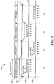
- a timing diagram 466 includes signals associated with integrator circuit 452. Signals p1, p2, swe, and swd described above are shown.
- the signal labeled V IN may correspond to input signal 453 and the signal labeled V OUT may correspond to output signal 462.
- Time periods T1 and T3 correspond to a measured time period during which integrator circuit 452 is processing measured magnetic field signal 204
- time periods T2 and T4 correspond to a reference time period during which integrator circuit 452 is processing reference magnetic field signal 206.
- V IN which corresponds to the measured, external magnetic field 106 during time period T1
- V IN has a value greater than zero during period T1.
- signals p1 and p2 couple and decouple input capacitor 458 to the inverting input of operational amplifier 464, the voltage across capacitors 454 will rise, as shown by the rising value of V OUT during time period T1.
- V OUT initially changes to the previous value stored on capacitors 456, which is zero in this example.
- V IN which corresponds to the reference magnetic field produced by coil 216 during time period T2 has a value greater than zero during time period T2.
- the amplitude of V IN during time period T2 is shown as lower than the amplitude during time period T1. In an embodiment, the lower amplitude may be due to the reference magnetic field having a relatively lower strength than the measured magnetic field 106.
- V OUT may rise at a slower rate during time period T2 due to the lower signal value V IN during this time period.
- V IN which corresponds to the measured, external magnetic field 106 during time period T3, has a value less than zero during period T3.
- the voltage across capacitors 454 decreases as shown by the decreasing value of the V OUT signal.
- V IN which corresponds to the reference magnetic field produced by coil 216 during time period T4, has a value less than zero during period T4.
- the voltage across capacitors 456 decreases as shown by the decreasing value of the V OUT signal.
- the value of V IN may be smaller during T4 than it is when processing the measured, external signal during T3.
- the value of the V OUT signal may decrease at a relatively slower rate during T4 than it does during T3.
- the voltage level across capacitors 456 (e.g. V OUT during time periods T2 and T4) can be compared to an expected value or expected threshold to generate a diagnostic output signal that can indicate whether a fault is present, for example. If V OUT falls outside of the threshold, a fault signal can be generated.
- the voltage level across capacitors 454, which corresponds to the measured magnetic field signal can be processed to determine position, speed, direction, and other aspects of magnetic target 102.
- the output signal of ADC 222 has a shape and/or value that is the same as or similar to the input signal to the ADC. Filtering the output signal to remove high-frequency components can also shape the output signal so that it more closely resembles the input signal. Thus, the output signal from ADC 222 can be compared to the input signal during the reference time period and. If the output signal deviates from the input signal by a predetermined amount or threshold, then a fault signal can be generated indicating that a fault has been detected. Other methods of generating the fault signal can also be used.
- capacitors 454 and 456 can periodically be swapped, so that capacitors 454 are used to process the reference magnetic field signal 206 during time periods T2 and T4, and capacitors 456 are used to process the measured magnetic field signal 204 during time periods T1 and T2. This can ensure that both sets of capacitors are used at one time or another to process the reference magnetic field signal, so that both sets of capacitors receive test coverage.
- the sets of capacitors can be swapped according to a predetermined time schedule, in response to a command received by magnetic field sensor 104, or according to any other method that allows the sets of capacitors to be swapped.
- control circuit 460 can swap capacitors 454 and 456 by swapping signals swe and swd.
- a reset signal (labeled as 'reset' in FIG. 9 ) is asserted between each transition between the measured and reference time periods.
- the reset signal may discharge any parasitic capacitors between each transition, and reduce or eliminate residual signals from the previous time period in order to reduce crosstalk and mixing between the measured and reference magnetic field signals.
- the clock signal (labeled 'adcclk') may be paused for a settling time to allow the magnetic field sensors, amplifier, and other circuits time to settle.
- inputs and outputs of operational amplifier 464 may be reset and capacitors 454 and 456 may be disconnected, i.e. decoupled from operational amplifier 464.
- capacitors 454 and 456 may also be reset if desired at power up or other times, by asserting the reset line while the capacitors are coupled to operational amplifier 464.
- Integrator operation includes sampling V IN from capacitor 458 and transferring charge from C IN to capacitor 454 (during the measured time period) or capacitor 456 (during the reference time period). Thus, with each sample, integrator 452 adds a scaled version of the input signal to a previous output voltage level.
- integrator 452 After a number of clock cycles, integrator 452 enters the reference time period and processes the reference signal.
- the number of clock signals may be chosen to be large enough to allow for the settling time and for oversampling of the signal being processed, and small enough to prevent leakage currents from altering the voltage stored on the capacitor 454 or 456 that is disconnected from operational amplifier 464 and is not being processed. As shown in FIG. 9 , the number of clock cycles is six. However, any number of appropriate clock cycles may be chosen.
- Signal V OUT may be sampled and stored on capacitor 454 or 456 on the falling edge of the clock adc_clk.
- the magnetic field sensing element may switch from a measured mode as shown in diagram 300 to a reference mode as shown in diagram 302 (See FIG. 3 ), and the inputs and outputs of operational amplifier 464 may be reset.
- capacitor 456 may be coupled to operational amplifier 464 to allow integrator circuit 452 to process the reference magnetic field signal.
- the slower rise in V OUT during time period T2 may be due to a smaller value of the diagnostic signal at V IN , which may correspond to the reference magnetic field having a relatively lower strength.
- integrator 452 may enter measured time period T3 and once again process the measured magnetic field signal 204 in the manner described above. Finally, as shown in FIG. 9 , at the end of time period T3, integrator 452 may enter reference time period T4 and once again process the reference magnetic field signal 206 in the manner described above.
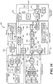
- a magnetic field sensor 500 includes a calibration circuit 510 that is responsive to a digital measured magnetic field signal 512 and to a digital reference magnetic field signal 514 to generate a calibrated magnetic field signal 520.
- the calibrated magnetic field signal 520 is further processed to generate an output signal 540 of the sensor that is indicative of the external magnetic field.
- the digital measured magnetic field signal 512 and the digital reference magnetic field signal 514 can be the same as or similar to signals 204 and 206 described above and thus, can be generated by switching between an external mode of operation in which a measured magnetic field signal 516 is generated by magnetic field sensing elements 526, such as the illustrated Hall effect elements, under the control of a Hall driver 532 and a reference mode of operation in which a reference magnetic field signal 518 is generated by a reference coil 528 under the control of a coil driver 530.
- the reference coil 528 is configured to carry a reference current to generate the reference magnetic field.
- At least one, and in the illustrated embodiment two, magnetic field sensing elements 526 are thus configurable to generate the measured magnetic field signal 516 during a first time period and to generate the reference magnetic field signal 518 during a second, non-overlapping time period.
- the measured magnetic field signal and the reference magnetic field signal may be processed by a Front End (FE) amplifier 524 that may be the same as or similar to amplifier 214 of FIG. 2 and converted into respective digital signals 512, 514 by an analog-to-digital converter 536 using a fixed reference from a voltage reference 592, which converter 536 can be the same as or similar to converter 222 of FIG. 2 .
- FE Front End
- the digital measured magnetic field signal 512 is filtered by a filter 544 to provide a filtered digital measured magnetic field signal 548 (referred to herein alternatively as the digital measured magnetic field signal) and the digital reference magnetic field signal 514 is filtered by a filter 546 to provide a filtered reference magnetic field signal 550 (referred to herein alternatively as the digital reference magnetic field signal).
- the digital measured magnetic field signal 512 has a larger amplitude than the digital reference magnetic field signal 514 and thus, filter 546 provides a higher degree of filtering than filter 544 to more accurately distinguish the reference magnetic field signal in the presence of noise.
- filters 544, 546 is a decimation low pass FIR filter.
- the calibration circuit 510 is configured to combine the digital measured magnetic field signal 548 and the digital reference magnetic field signal 550 in a manner that generates the calibrated magnetic field signal 520 with a reduced or eliminated dependence on certain influences on the magnetic field sensor 500.
- certain mechanical stresses on the package due to temperature and humidity variations can cause the sensor output signal 540 to vary from its nominal, trimmed value for a given external magnetic field, thereby adversely affecting the accuracy of the sensor.
- Operation of the calibration circuit 510 may be controlled by a master control circuit 542 (which additionally may control various other circuit functionality) and will be described in greater detail in connection with FIGS. 11-13 . Suffice it to say here that the calibration circuit 510 operates on the digital measured magnetic field signal 548 in a manner dependent on the digital reference magnetic field signal 550 to provide the calibrated signal 520 with a reduced or eliminated dependence on certain adverse influences.
- the calibrated magnetic field signal 520 may be processed by a linearization circuit 522 in certain applications.
- the calibrated signal 520 may be transformed into a signal representative of a position of a target by correlating values of the calibrated signal to values stored in a lookup table.
- the output of the linearization circuit 522 may be clamped by a clamp 552 to limit the output to a programmable range and further processed by a PWM/SENT encoder circuit 554 to generate a signal having a PWM format with a programmable frequency or a SENT signal format.
- a multiplexer 556 can be used to select between providing the output of the PWM/SENT circuit 554 or an output of a serial interface circuit 558 to an output signal generator 570.
- Additional elements of the magnetic field sensor 500 can include an analog Built-in-Self-Test (BIST) circuit 560 as may implement the above-described techniques for diagnostic signal processing to detect errors in the analog front end of the sensor, an EEPROM BIST circuit 562 to test the EEPROM 594, and a logic BIST circuit 564 to test various logic functionality on the sensor IC 500.
- BIST Built-in-Self-Test
- the output signal generator 570 is coupled to the multiplexer 556 and includes various elements used to reliably generate the sensor output signal 540 indicative of the external magnetic field, such as a slew control circuit 572, an output driver 574, a current limit circuit 576, an ESD protection device 578, and a serial Receiver (RX) circuit 580.
- the serial receiver 580 may implement bidirectional communication as described in a U.S. Patent No. 8,5,77,634 , entitled "Systems and Methods for Synchronizing Sensor Data" which is assigned to the assignee of the present disclosure.
- the sensor 500 may further include additional supporting elements such as an EEPROM 594, a charge pump 582, a regulator and Power On Reset (POR) circuit 584, a level detector 586, an ESD protection device 588 and, a clock generator 590.
- additional supporting elements such as an EEPROM 594, a charge pump 582, a regulator and Power On Reset (POR) circuit 584, a level detector 586, an ESD protection device 588 and, a clock generator 590.
- a temperature sensor 596 senses the ambient temperature to which the sensor is subjected, converts the sensed temperature into a digital signal, and provides the digital sensed temperature signal 598 to a temperature filter and trim circuit 600 for further coupling to the calibration circuit 510 as described below.
- the senor 500 may be provided in the form of an integrated circuit with an analog front end portion and a digital portion, it will be appreciated that the particular delineation of which circuit functions are implemented in an analog fashion or with digital circuitry and signals can be varied. Further, some of the illustrated circuit functions can be implemented on an integrated circuit sensor 500 and other circuitry and functionality can be implemented on separate circuits (e.g., additional substrates within the same integrated circuit package, or additional integrated circuit packages, and/ or on circuit boards).
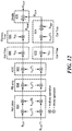
- the calibration circuit 510 and certain other elements of the sensor of FIG. 10 are shown.
- the filter 544 ( FIG. 10 ) that operates to filter the digital measured magnetic field signal 512 to provide the filtered digital measured magnetic field signal 548 is here shown to include a decimation filter 602, an ADC filter 604, and a bandwidth select filter 606, each providing low-pass filtering to reduce noise.
- filter 602 decimates a 2MHz ADC signal to 128kHz and provides some low-pass filtering. Slower (i.e., 128kHz) processing consumes less power and silicon area.
- Filter 604 provides additional low-pass filtering beyond what is feasible with the decimation filter 602 and filter 606 provides additional low-pass filtering that is selectable by the customer in order to permit a trade-off to be made between noise performance and response time.
- the reference path filter 546 ( FIG. 10 ) that operates to filter the digital reference magnetic field signal 514 to provide the filtered digital reference magnetic field signal 550 may be a decimation filter.
- the output of the bandwidth select filter 606 provides the filtered digital measured magnetic field signal 548 and is shown to be coupled to the calibration circuit 510 through a switch 608.
- sampling of the signal 548 may be at a predetermined sample rate, such as the illustrated 16kHz, or alternatively may be at a different rate such as in response to an external trigger signal as described in the above-referenced U.S. Patent No. 8,577,634 , for example.
- the temperature filter and trim circuit 600 is here shown to include a temperature decimation filter 610 and a temperature sensor trim circuit 612.
- the temperature sensor trim circuit 612 provides a trimmed factory temperature signal 614 for use by a factory trim circuit 624 and a reference trim circuit 640.
- the temperature sensor trim circuit also provides a trimmed customer temperature signal 616 for use by a customer trim circuit 644.
- Various schemes are possible to trimming the temperature signal 598.
- a post-linearization circuit 618 can be coupled between the linearization circuit 522 to introduce additional gain and offset trim, as may be useful to attenuate the signal to maintain usage of all linearization points when using an output range that is not full-scale for example.
- the calibration circuit 510 receives the digital measured magnetic field signal 548, the digital reference magnetic field signal 550, and the trimmed temperature signals 614, 616 and generates the calibrated signal 520, as shown. More particularly, the calibration circuit 510 includes factory trim circuit 624 (referred to alternatively as a manufacturing trim circuit) that receives the digital measured magnetic field signal 548 and the trimmed temperature signal 614 and is configured to adjust at least one of a gain or an offset of the digital measured magnetic field signal based on a sensed temperature (i.e., based on the trimmed temperature signal 614).
- factory trim circuit 624 referred to alternatively as a manufacturing trim circuit
- the factory trim circuit 624 corrects for analog front end gain and offset variations due to temperature, such as by adding a temperature-dependent offset and multiplying by a temperature-dependent gain factor, which factors may be programmed during a manufacturing test process.
- the factory trim circuit 624 may additionally correct for temperature-independent offset and gain errors in the analog front end signal path.
- Programmable trim values associated with the factory trim circuit and any other trim circuits can be programmed into EEPROM locations 594.
- the calibration circuit 510 further includes a reference trim circuit 640 that receives the digital reference magnetic field signal 550 and the trimmed temperature signal 614 and provides a trimmed reference magnetic field signal to a reference filter 642.
- the reference trim circuit 640 is configured to adjust a gain of the reference magnetic field signal 550. In one embodiment, the reference trim circuit 640 adjusts a gain of the digital reference magnetic field signal based on a predetermined scale factor to facilitate signal processing by a combining circuit 630, as will be described. The reference trim circuit 640 may further adjust at least one of the gain or an offset of the digital reference magnetic field signal based on a sensed temperature (i.e., based on trimmed temperature signal 614) in a manner that is the same as or similar to the factory trim circuit 624.
- a sensed temperature i.e., based on trimmed temperature signal 614
- the reference trim circuit 640 may correct for analog front end gain and offset variations due to temperature by adding a temperature-dependent offset and multiplying by a temperature-dependent gain factor, which factors may be programmed during a manufacturing test process.
- the reference trim circuit 640 may additionally correct for temperature-independent offset and gain errors in the analog front end signal path.
- programmable trim values can be programmed into EEPROM locations 594.
- the combining circuit 630 is configured to combine the digital measured magnetic field signal 548 and the digital reference magnetic field signal 550 and, more particularly, may operate to combine the trimmed version of these signals as labeled 626, 628, respectively, as shown.
- the combining circuit 630 divides the measured magnetic field signal 626 by the reference magnetic field signal 628.
- the division operation can be accomplished in various ways. In the illustrative embodiment, a Taylor series expansion is used as will be described.
- the output of the combining circuit 630 may be further trimmed by a customer trim circuit 644 in order to generate the calibrated magnetic field signal 520.
- the customer trim circuit 644 may be divided into a sensitivity trim portion which multiplies the input signal by a user programmable temperature-dependent gain factor and an offset portion that adds to its input a user programmable offset that is linearly dependent on temperature as a function of magnetic field strengths and offsets in the customer's application. Further processing of the calibrated signal 520 may be performed by linearization circuit 522, post-linearization circuit 618, clamp 552 and PWM/SENT encoder 554 ( FIG. 10 ).
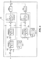
- FIG. 12 a model of the magnetic field sensor 500 ( FIGS. 10 and 11 ) is shown to illustrate the principle of operation of the combining circuit 630. As explained above, much of the sensor circuitry is shared between sensing and processing a magnetic field signal based on an external magnetic field B EXT and sensing and processing a magnetic field signal based on a reference magnetic field B CAL ; however, for simplicity of explanation, these two signal processing functions are shown in the model of FIG. 12 as being separate signal paths.
- the one or more magnetic field sensing elements 526 are represented by model block 654 as being responsive to an external magnetic field B EXT and a reference magnetic field B CAL as may be provided by a reference coil 528 ( FIG. 10 ) for example.
- the reference magnetic field B CAL is modeled as a function of temperature (T) because it is generated by temperature-sensitive components.
- the magnetic field sensing element is modeled with a temperature-dependent sensitivity k H1 (T) and a stress-dependent sensitivity multiplier of k H2 (S), where "S" represents mechanical stress.
- k H2 (S) represents the percentage change in nominal sensing element sensitivity k H2 due to stress, which is typically less than 3%. In other words, typically 0.97 ⁇ k H2 (S) ⁇ 1.03.
- the amplifier 524 and analog-to-digital converter 536 are modeled by respective blocks 658 and 662, each having a temperature-dependent gain k A (T) and k D (T), respectively.
- the external filter 544 ( FIG. 10 ) and the reference filter 546 ( FIG. 10 ) are modeled by respective blocks 666 and 672, each having a temperature-independent gain parameter k FE and k FC , respectively.
- the factory trim circuit 624 ( FIG. 11 ) is modeled by a block 668 as having a temperature dependent gain k TE (T).
- the reference trim circuit 640 ( FIG. 11 ) is modeled by a block 674 and includes a temperature dependent gain term k TC (T).
- Block 674 includes an additional term D REF to represent a gain adjustment by a predetermined reference value, or scale factor used to facilitate operation of the combining circuit 630 ( FIG. 11 ).
- Reference value D REF may be chosen to be an exponent of two to facilitate a simple division operation (i.e., a bit-shift operation) by the reference trim circuit 640.
- the combining circuit 630 ( FIG. 11 ) is modeled by a block 670 and is shown to compute D OUT , the quotient of the measured magnetic field signal 626 and the reference magnetic field signal 628, for further signal processing.
- the trim circuits 624, 640 are designed to reduce or remove the temperature dependence of the output signal.
- the k TE (T) and k TC (T) can be chosen so that: k TE T ⁇ k NOM ⁇ k FE ⁇ k H 1 T ⁇ k A T ⁇ k D T ⁇ 1 k TC T ⁇ D REF ⁇ k FC ⁇ k H 1 T ⁇ k A T ⁇ k D T ⁇ B EXT T ⁇ 1 where k NOM is the nominal, or desired, sensitivity of the sensor, independent of temperature and stress.
- k NOM defines how many LSBs the device output should change by in the presence of an input magnetic field change of 1 Gauss.
- equation (2) if the combined effect of the front-end parameters (which may be measured during manufacture) is known, then k TE (as a function of temperature) can be selected to make the sensitivity become k NOM , as desired.
- D OUT becomes the desired response, with desired sensitivity k NOM , independent of temperature (T) and stress (S).
- the model of FIG. 12 includes only operations that adjust the gain of the measured and reference signals. Temperature-dependent offsets also exist in the system, both as generated by inaccurate analog circuit components and as included for compensating for inaccurate analog circuit components by factory and reference trim blocks. These effects are not included in the model to simplify the above analysis. It will be appreciated that these offset errors can be cancelled in a similar way to the sensitivity error cancellations shown in Equations (2) through (4) above, resulting in a sensor output signal D OUT that remains independent of stress effects.
- the division operation performed by the combining circuit 630 can be simplified by forcing the divisor to be numerically close to one (e.g., within about 3%) as is achieved by the reference trim circuit 640 adjusting the gain of the reference magnetic field signal by the predetermined scale factor D REF .
- This simplification is possible because the reference trim circuit 640 forces D DEN ⁇ 1, thereby ensuring that the three terms used in the Taylor series approximation provide a resulting calibrated signal 520 that is accurate enough to track small changes in D DEN due to stresses.
- FIG. 13 shows a flowchart illustrating a process for implementing the magnetic field sensor 500 ( FIGS. 10 and 11 ) to calibrate a measured magnetic field signal.
- Rectangular elements herein denoted “processing blocks” represent computer software instructions or groups of instructions.
- Diamond shaped elements herein denoted “decision blocks,” represent computer software instructions, or groups of instructions, which affect the execution of the computer software instructions represented by the processing blocks.
- the processing and decision blocks represent steps performed by functionally equivalent circuits such as a digital signal processor circuit or an application specific integrated circuit (ASIC).
- ASIC application specific integrated circuit
- the process 700 commences with a measured magnetic field signal (e.g., signal 516 of FIG. 10 ) being generated in response to an external magnetic field at block 702, as may be achieved with the Hall effect elements 526 configured to respond only to an external magnetic field.
- a reference magnetic field signal (e.g., signal 518 of FIG. 10 ) is generated in response to a reference magnetic field at block 712, as may also be achieved with the Hall effect elements 526 configured to respond to reference magnetic field such as the reference magnetic field generated by reference coil 528.
- the magnetic field sensing elements 526 are configured to generate the measured magnetic field signal 516 during a first timer period and to generate the reference magnetic field signal 518 during a second, non-overlapping time period.
- the measured and reference magnetic field signals are converted to digital signals (e.g., signals 512, 514 of FIG. 10 ) in process blocks 704 and 714, respectively, as may be achieved with the analog-to-digital converter 536 ( FIG. 10 ), and the measured and reference magnetic field signals may be filtered in blocks 706, 716, respectively, by filters 544, 546 (e.g., to provide signals 548, 550 of FIG. 10 ).
- filters 544, 546 e.g., to provide signals 548, 550 of FIG. 10
- at least one of a gain or offset of the external magnetic field signal 548 may be adjusted, such as by factory trim circuit 624 ( FIG. 11 ).
- a gain of the reference magnetic field signal 550 may be adjusted by a predetermined scale factor and also or alternatively a gain or offset of the reference magnetic field signal 550 may be adjusted, such as by reference trim circuit 640 ( FIG. 11 ).
- the digital measured magnetic field signal 626 and the digital reference magnetic field signal 628 are combined to generate a calibrated magnetic field signal in block 720, such as may be achieved by combining circuit 630 ( FIG. 11 ). Accordingly, in one embodiment, the digital measured magnetic field signal 626 is divided by the digital reference magnetic field signal 628. It will be appreciated that other schemes for combining the digital measured magnetic field signal 626 and the digital reference magnetic field signal 628 may be possible in order to still achieve the reduction or elimination of stress influences on the generated calibrated signal.
- the calibrated magnetic field signal (e.g., signal 520 in FIG. 10 ) is used to generate the sensor output signal (e.g., signal 540 in FIG. 10 ).
- the calibration process 700 may be performed at any time since the related circuitry and processing is integrated within the sensor 500 (e.g., on an integrated circuit sensor 500). Furthermore, the process steps may be performed together or in stages. For example, some portions of the signal processing may be performed during the manufacturing process (e.g., processing performed by the factory trim circuit 624, the customer trim circuit 644, the reference trim circuit 640, and/or the temperature sensor trim circuit 612) while other signal processing (e.g., the signal combining by combining circuit 630) may be performed periodically or in response to a command signal during use of the sensor after it is installed in the intended environment.
- the manufacturing process e.g., processing performed by the factory trim circuit 624, the customer trim circuit 644, the reference trim circuit 640, and/or the temperature sensor trim circuit 612
- other signal processing e.g., the signal combining by combining circuit 630
- processing blocks illustrated in FIG. 13 may occur simultaneously rather than sequentially and that the illustrated sequence can be varied in many instances.
- the calibration circuit 510 FIGs. 10 and 11
- the calibration circuit 510 FIGs. 10 and 11
- the analog-to-digital conversion by converter 536 it will be appreciated that the same calibration concepts can be applied in the analog domain.
- the division performed by the combining circuit 630 alternatively could be performed in the analog domain with the use of an analog-to-digital converter that has as its input the measured magnetic field signal 516 ( FIG. 10 ) and as its reference the reference magnetic field signal 518.
- the analog-to-digital conversion blocks 704, 714 in FIG. 13 can occur later in the process, after the measured magnetic field signal is divided by the reference magnetic field signal.
Landscapes
- Physics & Mathematics (AREA)
- General Physics & Mathematics (AREA)
- Condensed Matter Physics & Semiconductors (AREA)
- Engineering & Computer Science (AREA)
- Computer Hardware Design (AREA)
- Microelectronics & Electronic Packaging (AREA)
- General Engineering & Computer Science (AREA)
- Measuring Magnetic Variables (AREA)
Claims (21)
- Magnetfeldsensor (104), umfassend:mindestens ein Magnetfeldsensorelement (202), das konfiguriert ist, ein Magnetfeldmesssignal (204) in Reaktion auf ein externes Magnetfeld zu erzeugen, und ein Magnetfeldreferenzsignal (206) in Reaktion auf ein Referenzmagnetfeld zu erzeugen;mindestens einen Analog-Digital-Konverter (222), der in Reaktion auf das Magnetfeldmesssignal ein digitales Magnetfeldmesssignal erzeugt, und in Reaktion auf das Magnetfeldreferenzsignal ein digitales Magnetfeldreferenzsignal erzeugt; undeine Kalibrierschaltung (510), die in Reaktion auf das digitale Magnetfeldmesssignal und das digitale Magnetfeldreferenzsignal das digitale Magnetfeldmesssignal und das digitale Magnetfeldreferenzsignal kombiniert, um ein kalibriertes Magnetfeldsignal (520) zu erzeugen,dadurch gekennzeichnet, dass die Kalibrierschaltung einen Teiler (630) umfasst, der konfiguriert ist, das digitale Magnetfeldmesssignal durch das digitale Magnetfeldreferenzsignal zu teilen, um das kalibrierte Magnetfeldsignal zu erzeugen.
- Magnetfeldsensor nach Anspruch 1, ferner eine Referenzspule (528) in Nähe des mindestens einen Magnetfeldsensorelements (202) umfassend, wobei die Spule konfiguriert ist, einen Referenzstrom zu tragen, um das Referenzmagnetfeld zu erzeugen.
- Magnetfeldsensor nach Anspruch 1, wobei das mindestens eine Magnetfeldsensorelement (202) konfigurierbar ist, das Magnetfeldmesssignal während einer ersten Zeitspanne zu erzeugen, und das Magnetfeldreferenzsignal während einer zweiten, nicht überschneidenden Zeitspanne zu erzeugen.
- Magnetfeldsensor nach Anspruch 1, wobei das mindestens eine Magnetfeldsensorelement (202) ein Hall-Effekt-Element umfasst.
- Magnetfeldsensor nach Anspruch 1, wobei das mindestens eine Magnetfeldsensorelement (202) ein Magnetwiderstandselement umfasst.
- Magnetfeldsensor nach Anspruch 1, ferner umfassend eine eingebaute Selbsttestschaltung (560), die konfiguriert ist, einen Fehler in dem Magnetfeldsensor festzustellen.
- Magnetfeldsensor nach Anspruch 1, ferner einen Ausgangssignalgenerator (570) umfassend, der in Reaktion auf das kalibrierte Magnetfeldsignal ein Ausgangssignal (540) des Magnetfeldsensors erzeugt, welches das externe Magnetfeld anzeigt.
- Magnetfeldsensor nach Anspruch 1, ferner umfassend eine Herstellungstrimschaltung (600), die konfiguriert ist, mindestens eine Verstärkung und/oder ein Offset des digitalen Magnetfeldmesssignals basierend auf einer erfassten Temperatur anzupassen.
- Magnetfeldsensor nach Anspruch 1, ferner eine Kalibrierungstrimschaltung (640) umfassend, die konfiguriert ist, eine Verstärkung des digitalen Magnetfeldreferenzsignals basierend auf einem vorbestimmten Skalierungsfaktor anzupassen.
- Magnetfeldsensor nach Anspruch 9, wobei die Kalibrierungstrimschaltung (640) ferner konfiguriert ist, mindestens die Verstärkung und/oder ein Offset des digitalen Magnetfeldreferenzsignals basierend auf einer erfassten Temperatur anzupassen.
- Magnetfeldsensor nach Anspruch 1, wobei der Teiler (630) einen Multiplizierer umfasst, der konfiguriert ist, das kalibrierte Magnetfeldsignal basierend auf einer Taylorreihenentwicklung zu erzeugen.
- Magnetfeldsensor nach Anspruch 1, wobei das mindestens eine Magnetfeldsensorelement mindestens zwei Magnetfeldsensorelemente umfasst, die aus Hall-Effekt-Elementen, Magnetwiderstandselementen, oder aus beiden derselben, ausgewählt sind.
- Magnetfeldsensor nach Anspruch 1, wobei die Kalibrierungsschaltung (510) einen Multiplizierer umfasst, der konfiguriert ist, das kalibrierte Magnetfeldsignal basierend auf einer Taylorreihenentwicklung zu erzeugen.
- Verfahren zum Kalibrieren eines erfassten Magnetfeldsignals, umfassend:Erzeugen eines Magnetfeldmesssignals (204), das eine Amplitude in Abhängigkeit eines externen Magnetfelds aufweist;Erzeugen eines gemessenen Magnetfeldreferenzsignals (206), das eine Amplitude in Abhängigkeit eines Referenzmagnetfelds aufweist;Umwandeln des Magnetfeldmesssignals in ein digitales Magnetfeldmesssignal und Umwandeln des Magnetfeldreferenzsignals in ein digitales Magnetfeldreferenzsignal; undKombinieren des digitalen Magnetfeldmesssignals und des digitalen Magnetfeldreferenzsignals zum Erzeugen eines kalibrierten Signals (520),dadurch gekennzeichnet, dass das Kombinieren Teilen des digitalen Magnetfeldmesssignals durch das digitale Magnetfeldreferenzsignal zum Erzeugen des kalibrierten Signals umfasst.
- Verfahren nach Anspruch 14, ferner umfassend das Anpassen mindestens eine Verstärkung und/oder ein Offset des digitalen Magnetfeldmesssignals basierend auf einer erfassten Temperatur.
- Verfahren nach Anspruch 14, ferner umfassend das Anpassen einer Verstärkung des digitalen Magnetfeldreferenzsignals basierend auf einem vorbestimmten Skalierungsfaktor.
- Verfahren nach Anspruch 16, wobei das Anpassen ferner ein Anpassen mindestens der Verstärkung und/oder eines Offsets des digitalen Magnetfeldreferenzsignals basierend auf einer erfassten Temperatur umfasst.
- Verfahren nach Anspruch 14, wobei das Teilen Multiplizieren einer Vielzahl von Termen gemäß einer Taylorreihenentwicklung umfasst.
- Verfahren nach Anspruch 14, wobei mindestens das Erzeugen des Magnetfeldmesssignals und/oder Erzeugen des Magnetfeldreferenzsignals das Verwenden mindestens eines Hall-Effekt-Elements umfasst.
- Verfahren nach Anspruch 14, wobei mindestens eines aus Erzeugen des Magnetfeldmesssignals oder Erzeugen des Magnetfeldreferenzsignals das Verwenden mindestens eines Magnetwiderstandselements umfasst.
- Verfahren nach Anspruch 14, ferner umfassend das Feststellen eines Fehlers mit einer eingebauten Selbsttestschaltung (560).
Applications Claiming Priority (2)
| Application Number | Priority Date | Filing Date | Title |
|---|---|---|---|
| US14/541,735 US9841485B2 (en) | 2014-11-14 | 2014-11-14 | Magnetic field sensor having calibration circuitry and techniques |
| PCT/US2015/057464 WO2016077065A1 (en) | 2014-11-14 | 2015-10-27 | Magnetic field sensor having calibration circuitry and techniques |
Publications (3)
| Publication Number | Publication Date |
|---|---|
| EP3213036A1 EP3213036A1 (de) | 2017-09-06 |
| EP3213036B1 true EP3213036B1 (de) | 2018-07-04 |
| EP3213036B8 EP3213036B8 (de) | 2018-08-15 |
Family
ID=54478980
Family Applications (1)
| Application Number | Title | Priority Date | Filing Date |
|---|---|---|---|
| EP15791840.0A Active EP3213036B8 (de) | 2014-11-14 | 2015-10-27 | Magnetfeldsensor mit kalibrierungsschaltung und -techniken |
Country Status (4)
| Country | Link |
|---|---|
| US (1) | US9841485B2 (de) |
| EP (1) | EP3213036B8 (de) |
| JP (2) | JP2017534063A (de) |
| WO (1) | WO2016077065A1 (de) |
Families Citing this family (57)
| Publication number | Priority date | Publication date | Assignee | Title |
|---|---|---|---|---|
| US9817078B2 (en) | 2012-05-10 | 2017-11-14 | Allegro Microsystems Llc | Methods and apparatus for magnetic sensor having integrated coil |
| US10145908B2 (en) | 2013-07-19 | 2018-12-04 | Allegro Microsystems, Llc | Method and apparatus for magnetic sensor producing a changing magnetic field |
| US10284217B1 (en) | 2014-03-05 | 2019-05-07 | Cirrus Logic, Inc. | Multi-path analog front end and analog-to-digital converter for a signal processing system |
| US9791521B2 (en) * | 2014-03-27 | 2017-10-17 | Texas Instruments Incorporated | Systems and methods for operating a hall-effect sensor without an applied magnetic field |
| US9596537B2 (en) | 2014-09-11 | 2017-03-14 | Cirrus Logic, Inc. | Systems and methods for reduction of audio artifacts in an audio system with dynamic range enhancement |
| US9804222B2 (en) * | 2014-11-14 | 2017-10-31 | Allegro Microsystems, Llc | Magnetic field sensor with shared path amplifier and analog-to-digital-converter |
| US9774442B2 (en) * | 2015-04-03 | 2017-09-26 | Denso Corporation | Communication device |
| US20170200351A1 (en) * | 2016-01-11 | 2017-07-13 | Robert Grubba | Sound-Producing Shoe Including Impact and Proximity Detections |
| US10132879B2 (en) | 2016-05-23 | 2018-11-20 | Allegro Microsystems, Llc | Gain equalization for multiple axis magnetic field sensing |
| US9998826B2 (en) | 2016-06-28 | 2018-06-12 | Cirrus Logic, Inc. | Optimization of performance and power in audio system |
| US10545561B2 (en) * | 2016-08-10 | 2020-01-28 | Cirrus Logic, Inc. | Multi-path digitation based on input signal fidelity and output requirements |
| US10263630B2 (en) | 2016-08-11 | 2019-04-16 | Cirrus Logic, Inc. | Multi-path analog front end with adaptive path |
| US9929703B1 (en) | 2016-09-27 | 2018-03-27 | Cirrus Logic, Inc. | Amplifier with configurable final output stage |
| US10216559B2 (en) * | 2016-11-14 | 2019-02-26 | Allegro Microsystems, Llc | Diagnostic fault communication |
| EP3321638B1 (de) * | 2016-11-14 | 2019-03-06 | Melexis Technologies SA | Messung einer absoluten winkelposition |
| US9999107B1 (en) * | 2016-12-14 | 2018-06-12 | Allegro Microsystems, Llc | Light emitting diode driver for dimming and on/off control |
| EP3367067B1 (de) * | 2017-02-28 | 2019-07-03 | Melexis Technologies SA | Positionssensor und positionserfassungsverfahren |
| US10321230B2 (en) | 2017-04-07 | 2019-06-11 | Cirrus Logic, Inc. | Switching in an audio system with multiple playback paths |
| US10008992B1 (en) | 2017-04-14 | 2018-06-26 | Cirrus Logic, Inc. | Switching in amplifier with configurable final output stage |
| US10837943B2 (en) | 2017-05-26 | 2020-11-17 | Allegro Microsystems, Llc | Magnetic field sensor with error calculation |
| US11428755B2 (en) * | 2017-05-26 | 2022-08-30 | Allegro Microsystems, Llc | Coil actuated sensor with sensitivity detection |
| US10996289B2 (en) | 2017-05-26 | 2021-05-04 | Allegro Microsystems, Llc | Coil actuated position sensor with reflected magnetic field |
| US10859399B2 (en) * | 2017-06-15 | 2020-12-08 | Standex International Corporation | Method and apparatus for magnetically sensing the position of a magnetic target |
| EP3457154B1 (de) * | 2017-09-13 | 2020-04-08 | Melexis Technologies SA | Streufeldabstossung in magnetischen sensoren |
| CN107783034B (zh) * | 2017-09-14 | 2020-07-10 | 云南电网有限责任公司保山供电局 | 一种单柱式高压隔离开关状态在线监测装置及方法 |
| EP3470862B1 (de) * | 2017-10-10 | 2022-03-02 | Melexis Bulgaria Ltd. | Sensordefektdiagnoseschaltung |
| US10578681B2 (en) * | 2017-10-26 | 2020-03-03 | Infineon Technologies Ag | Sensors using digitally assisted 1/x analog gain compensation |
| US10466314B2 (en) * | 2018-02-15 | 2019-11-05 | Hamilton Sundstrand Corporation | Integrated current sensor |
| US10677620B2 (en) * | 2018-05-01 | 2020-06-09 | Nxp B.V. | System and method for sensor diagnostics during functional operation |
| US10955493B2 (en) | 2018-05-02 | 2021-03-23 | Analog Devices Global Unlimited Company | Magnetic sensor systems |
| US10656170B2 (en) | 2018-05-17 | 2020-05-19 | Allegro Microsystems, Llc | Magnetic field sensors and output signal formats for a magnetic field sensor |
| US10725122B2 (en) | 2018-07-20 | 2020-07-28 | Allegro Microsystems, Llc | Ratiometric sensor output topology and methods |
| US12385762B2 (en) * | 2019-03-05 | 2025-08-12 | Infineon Technologies Ag | Multilayered safety mechanism for a three-phase off-axis angle sensor |
| DE102019115373A1 (de) | 2019-06-06 | 2020-12-10 | Infineon Technologies Ag | Sensorvorrichtungen mit testmagneten und zugehörige verfahren |
| US11867773B2 (en) * | 2019-06-18 | 2024-01-09 | Texas Instruments Incorporated | Switched capacitor integrator circuit with reference, offset cancellation and differential to single-ended conversion |
| WO2021102446A1 (en) * | 2019-11-24 | 2021-05-27 | Purdue Research Foundation | High accuracy non-invasive current sensor system |
| DE102019134077B4 (de) * | 2019-12-12 | 2021-07-22 | Infineon Technologies Ag | Signalverarbeitungsschaltung für einen Hall-Sensor und Signalverarbeitungsverfahren |
| US11942831B2 (en) | 2020-01-15 | 2024-03-26 | Allegro Microsystems, Llc | Three-phase BLDC motor driver/controller having diagnostic signal processing |
| US11169223B2 (en) | 2020-03-23 | 2021-11-09 | Allegro Microsystems, Llc | Hall element signal calibrating in angle sensor |
| US11262422B2 (en) | 2020-05-08 | 2022-03-01 | Allegro Microsystems, Llc | Stray-field-immune coil-activated position sensor |
| US11029370B1 (en) | 2020-05-22 | 2021-06-08 | Allegro Microsystems, Llc | Sensor output control methods and apparatus |
| LU102431B1 (de) * | 2021-01-15 | 2022-07-18 | Phoenix Contact Gmbh & Co | Verfahren und Vorrichtung zur Erfassung eines veränderten Messverhaltens einer Strommessvorrichtung mit einem Magnetkern und mindestens einen Sensor |
| US11493361B2 (en) | 2021-02-26 | 2022-11-08 | Allegro Microsystems, Llc | Stray field immune coil-activated sensor |
| JP2022151007A (ja) * | 2021-03-26 | 2022-10-07 | ローム株式会社 | 磁気センサ |
| US11630130B2 (en) | 2021-03-31 | 2023-04-18 | Allegro Microsystems, Llc | Channel sensitivity matching |
| US11885645B2 (en) | 2021-06-17 | 2024-01-30 | Allegro Microsystems, Llc | Supply voltage configurable sensor |
| US11578997B1 (en) | 2021-08-24 | 2023-02-14 | Allegro Microsystems, Llc | Angle sensor using eddy currents |
| JP7623925B2 (ja) | 2021-10-25 | 2025-01-29 | 三星電子株式会社 | 検査装置 |
| US11630169B1 (en) | 2022-01-17 | 2023-04-18 | Allegro Microsystems, Llc | Fabricating a coil above and below a magnetoresistance element |
| US11782105B2 (en) | 2022-01-17 | 2023-10-10 | Allegro Microsystems, Llc | Fabricating planarized coil layer in contact with magnetoresistance element |
| US12265137B2 (en) * | 2022-11-18 | 2025-04-01 | Allegro Microsystems, Llc | Diagnostic path for gain and offset calibration |
| EP4382941A1 (de) * | 2022-12-07 | 2024-06-12 | LX Semicon Co., Ltd. | Analoge frontend-schaltung und kameramodulsteuerungstreiber damit |
| US12253576B2 (en) | 2023-01-10 | 2025-03-18 | Allegro Microsystems, Llc | Self-calibrating magnetoresistance-based magnetic field sensors |
| US12510611B2 (en) | 2023-11-07 | 2025-12-30 | Allegro Microsystems, Llc | TMR sensor having magnetic field generation for pillar stimulation |
| US12455301B2 (en) | 2023-12-11 | 2025-10-28 | Allegro Microsystems, Llc | Hall plate current sensor having stress compensation |
| US12449279B2 (en) | 2024-02-07 | 2025-10-21 | Allegro Microsystems, Llc | Dynamic resolution sensor |
| US12523717B2 (en) | 2024-02-15 | 2026-01-13 | Allegro Microsystems, Llc | Closed loop magnetic field sensor with current control |
Family Cites Families (69)
| Publication number | Priority date | Publication date | Assignee | Title |
|---|---|---|---|---|
| GB2000639B (en) | 1977-06-29 | 1982-03-31 | Tokyo Shibaura Electric Co | Semiconductor device |
| DE3030620A1 (de) | 1980-08-13 | 1982-03-11 | Siemens AG, 1000 Berlin und 8000 München | Anordnung zur aenderung der elektrischen schaltungskonfiguration von integrierten halbleiterschaltkreisen |
| JPS58144281U (ja) | 1982-03-20 | 1983-09-28 | 株式会社島津製作所 | 地磁気測定器 |
| CH664632A5 (de) | 1984-08-16 | 1988-03-15 | Landis & Gyr Ag | Schaltungsanordnung zur kompensation von schwankungen des uebertragungsfaktors eines magnetfeldsensors. |
| US4833406A (en) | 1986-04-17 | 1989-05-23 | Household Commercial Financial Services Inc. | Temperature compensated Hall-effect sensor apparatus |
| FR2597592A1 (fr) * | 1986-04-21 | 1987-10-23 | Schrader | Procede de compensation en temperature de la mesure realisee par un capteur magnetique |
| US4760285A (en) | 1987-03-30 | 1988-07-26 | Honeywell Inc. | Hall effect device with epitaxal layer resistive means for providing temperature independent sensitivity |
| FR2614695B1 (fr) | 1987-04-28 | 1989-06-23 | Commissariat Energie Atomique | Procede de numerisation et de linearisation d'un capteur a caracteristique periodique quasi sinusoidale et dispositif correspondant |
| JPS63282568A (ja) * | 1987-05-13 | 1988-11-18 | Mitsubishi Heavy Ind Ltd | デ−タ処理方法 |
| US4823075A (en) | 1987-10-13 | 1989-04-18 | General Electric Company | Current sensor using hall-effect device with feedback |
| EP0338122B1 (de) | 1988-04-21 | 1993-03-10 | Landis & Gyr Business Support AG | Integrierte Halbleiterschaltung mit einem Magnetfeldsensor aus Halbleitermaterial |
| EP0357013A3 (de) | 1988-09-02 | 1991-05-15 | Honeywell Inc. | Schaltung zum Messen eines magnetischen Feldes |
| JPH03176682A (ja) * | 1989-12-06 | 1991-07-31 | Hitachi Ltd | 磁場計測装置 |
| JPH03248611A (ja) | 1990-02-27 | 1991-11-06 | Mitsubishi Electric Corp | 温度補償利得設定制御装置 |
| JPH0816692B2 (ja) | 1990-09-30 | 1996-02-21 | ダイキン工業株式会社 | 磁束ロック方法およびその装置 |
| DE4114835A1 (de) | 1991-05-07 | 1992-11-12 | Vdo Schindling | Schalteinrichtung, insbesondere zur verwendung in kraftfahrzeugen |
| US5381282A (en) * | 1991-10-18 | 1995-01-10 | International Business Machines Corporation | Inter-sample switching of servo control in direct access storage devices |
| US5247278A (en) | 1991-11-26 | 1993-09-21 | Honeywell Inc. | Magnetic field sensing device |
| JP3196943B2 (ja) * | 1992-08-14 | 2001-08-06 | フィガロ技研株式会社 | ガス検出装置 |
| US5469058A (en) | 1992-12-30 | 1995-11-21 | Dunnam; Curt | Feedback enhanced sensor, alternating magnetic field detector |
| JPH06281625A (ja) * | 1993-03-26 | 1994-10-07 | Nippon Steel Corp | 漏洩磁気探傷装置における感度校正装置 |
| GB2276727B (en) | 1993-04-01 | 1997-04-09 | Rolls Royce & Ass | Improvements in and relating to magnetometers |
| DE4319146C2 (de) | 1993-06-09 | 1999-02-04 | Inst Mikrostrukturtechnologie | Magnetfeldsensor, aufgebaut aus einer Ummagnetisierungsleitung und einem oder mehreren magnetoresistiven Widerständen |
| US5329416A (en) | 1993-07-06 | 1994-07-12 | Alliedsignal Inc. | Active broadband magnetic flux rate feedback sensing arrangement |
| US6104231A (en) | 1994-07-19 | 2000-08-15 | Honeywell International Inc. | Temperature compensation circuit for a hall effect element |
| JPH08201490A (ja) | 1995-01-31 | 1996-08-09 | Mitsumi Electric Co Ltd | センサic |
| DE19539458C2 (de) | 1995-10-24 | 2001-03-15 | Bosch Gmbh Robert | Sensor mit Testeingang |
| US5621319A (en) | 1995-12-08 | 1997-04-15 | Allegro Microsystems, Inc. | Chopped hall sensor with synchronously chopped sample-and-hold circuit |
| US6809515B1 (en) | 1998-07-31 | 2004-10-26 | Spinix Corporation | Passive solid-state magnetic field sensors and applications therefor |
| JP2000055999A (ja) | 1998-08-11 | 2000-02-25 | Tdk Corp | 磁気センサ装置および電流センサ装置 |
| US6545788B1 (en) * | 1999-03-09 | 2003-04-08 | Agere Systems, Inc. | Multiple path digital wavelength stabilization |
| US6436748B1 (en) | 1999-08-31 | 2002-08-20 | Micron Technology, Inc. | Method for fabricating CMOS transistors having matching characteristics and apparatus formed thereby |
| US6853178B2 (en) | 2000-06-19 | 2005-02-08 | Texas Instruments Incorporated | Integrated circuit leadframes patterned for measuring the accurate amplitude of changing currents |
| JP4310895B2 (ja) * | 2000-07-04 | 2009-08-12 | 株式会社島津製作所 | 磁気測定器 |
| US6750644B1 (en) * | 2000-09-06 | 2004-06-15 | General Electric Company | Magnetic field sensor and method for calibrating the same |
| JP2002213992A (ja) | 2001-01-23 | 2002-07-31 | Sumitomo Metal Mining Co Ltd | 非接触磁気式計測装置 |
| EP1260825A1 (de) | 2001-05-25 | 2002-11-27 | Sentron Ag | Magnetfeldsensor |
| JP3877998B2 (ja) | 2001-11-05 | 2007-02-07 | 株式会社山武 | 角度センサの温度情報検出装置および位置検出装置 |
| US6794863B2 (en) | 2002-11-13 | 2004-09-21 | Matsushta Electric Industrial Co., Ltd. | Magnetic field sensor, method for detecting magnetic field and device for detecting magnetic field |
| JP2004177228A (ja) | 2002-11-26 | 2004-06-24 | Matsushita Electric Works Ltd | 電流計測装置 |
| JP4349812B2 (ja) | 2003-02-03 | 2009-10-21 | 日本電産サンキョー株式会社 | 磁気センサ装置 |
| US7259545B2 (en) | 2003-02-11 | 2007-08-21 | Allegro Microsystems, Inc. | Integrated sensor |
| US7061221B2 (en) * | 2004-01-15 | 2006-06-13 | Bae Systems Information And Electronic Systems Integration Inc. | Reduced complexity transmission line and waveguide fault tester |
| EP1637898A1 (de) | 2004-09-16 | 2006-03-22 | Liaisons Electroniques-Mecaniques Lem S.A. | Dauerhaft kalibrierter Magnetfeldsensor |
| JP2008515043A (ja) | 2004-09-27 | 2008-05-08 | コーニンクレッカ フィリップス エレクトロニクス エヌ ヴィ | 入力装置用の磁気センサ |
| JP2006126012A (ja) | 2004-10-28 | 2006-05-18 | Asahi Kasei Microsystems Kk | 磁電変換システム及び磁電変換装置並びにその制御回路 |
| EP1679524A1 (de) | 2005-01-11 | 2006-07-12 | Ecole Polytechnique Federale De Lausanne Epfl - Sti - Imm - Lmis3 | Hallsensor und Verfahren zum Betrieb eines Hallsensors |
| KR100909925B1 (ko) | 2005-02-08 | 2009-07-29 | 로무 가부시키가이샤 | 자기 센서 회로 및 그 자기 센서 회로를 갖는 휴대 단말기 |
| DE102005047413B8 (de) | 2005-02-23 | 2012-05-10 | Infineon Technologies Ag | Magnetfeldsensorelement und Verfahren zum Durchführen eines On-Wafer-Funktionstests, sowie Verfahren zur Herstellung von Magnetfeldsensorelementen und Verfahren zur Herstellung von Magnetfeldsensorelementen mit On-Wafer-Funktionstest |
| US20070166245A1 (en) * | 2005-11-28 | 2007-07-19 | Leonard Mackles | Propellant free foamable toothpaste composition |
| WO2007138508A1 (en) | 2006-05-30 | 2007-12-06 | Koninklijke Philips Electronics N. V. | Sensor device with adaptive field compensation |
| DE102006045141B9 (de) | 2006-09-25 | 2009-02-19 | Infineon Technologies Ag | Magnetfeld-Sensor-Vorrichtung |
| US7425821B2 (en) | 2006-10-19 | 2008-09-16 | Allegro Microsystems, Inc. | Chopped Hall effect sensor |
| CN200986484Y (zh) | 2006-11-28 | 2007-12-05 | 李彩珍 | 磁场传感器 |
| US7605580B2 (en) | 2007-06-29 | 2009-10-20 | Infineon Technologies Austria Ag | Integrated hybrid current sensor |
| US7973635B2 (en) | 2007-09-28 | 2011-07-05 | Access Business Group International Llc | Printed circuit board coil |
| US7923996B2 (en) | 2008-02-26 | 2011-04-12 | Allegro Microsystems, Inc. | Magnetic field sensor with automatic sensitivity adjustment |
| EP2108966A1 (de) * | 2008-04-08 | 2009-10-14 | Ecole Polytechnique Fédérale de Lausanne (EPFL) | Stromsensor und Baugruppe zur Strommessung |
| WO2010096367A1 (en) | 2009-02-17 | 2010-08-26 | Allegro Microsystems, Inc. | Circuits and methods for generating a self-test of a magnetic field sensor |
| EP2634592B1 (de) | 2009-07-22 | 2015-01-14 | Allegro Microsystems, LLC | Schaltungen und Verfahren zur Herstellung eines diagnostischen Betriebsmodus bei einem Magnetfeldsensor |
| JP5481131B2 (ja) | 2009-08-31 | 2014-04-23 | 電気化学工業株式会社 | ブロー成形に適したビニル芳香族炭化水素系樹脂組成物 |
| JP5524796B2 (ja) * | 2010-09-30 | 2014-06-18 | 株式会社ダイヘン | 高周波測定装置、および、高周波測定装置の校正方法 |
| US8350563B2 (en) * | 2010-10-12 | 2013-01-08 | Allegro Microsystems, Inc. | Magnetic field sensor and method used in a magnetic field sensor that adjusts a sensitivity and/or an offset over temperature |
| US8577634B2 (en) | 2010-12-15 | 2013-11-05 | Allegro Microsystems, Llc | Systems and methods for synchronizing sensor data |
| US8680846B2 (en) | 2011-04-27 | 2014-03-25 | Allegro Microsystems, Llc | Circuits and methods for self-calibrating or self-testing a magnetic field sensor |
| US8890518B2 (en) | 2011-06-08 | 2014-11-18 | Allegro Microsystems, Llc | Arrangements for self-testing a circular vertical hall (CVH) sensing element and/or for self-testing a magnetic field sensor that uses a circular vertical hall (CVH) sensing element |
| US8604777B2 (en) * | 2011-07-13 | 2013-12-10 | Allegro Microsystems, Llc | Current sensor with calibration for a current divider configuration |
| US9201122B2 (en) | 2012-02-16 | 2015-12-01 | Allegro Microsystems, Llc | Circuits and methods using adjustable feedback for self-calibrating or self-testing a magnetic field sensor with an adjustable time constant |
| US8754640B2 (en) | 2012-06-18 | 2014-06-17 | Allegro Microsystems, Llc | Magnetic field sensors and related techniques that can provide self-test information in a formatted output signal |
-
2014
- 2014-11-14 US US14/541,735 patent/US9841485B2/en active Active
-
2015
- 2015-10-27 JP JP2017525896A patent/JP2017534063A/ja active Pending
- 2015-10-27 EP EP15791840.0A patent/EP3213036B8/de active Active
- 2015-10-27 WO PCT/US2015/057464 patent/WO2016077065A1/en not_active Ceased
-
2019
- 2019-09-25 JP JP2019173736A patent/JP6865799B2/ja active Active
Non-Patent Citations (1)
| Title |
|---|
| None * |
Also Published As
| Publication number | Publication date |
|---|---|
| WO2016077065A1 (en) | 2016-05-19 |
| JP2020073877A (ja) | 2020-05-14 |
| JP2017534063A (ja) | 2017-11-16 |
| JP6865799B2 (ja) | 2021-04-28 |
| US9841485B2 (en) | 2017-12-12 |
| EP3213036B8 (de) | 2018-08-15 |
| EP3213036A1 (de) | 2017-09-06 |
| US20160139230A1 (en) | 2016-05-19 |
Similar Documents
| Publication | Publication Date | Title |
|---|---|---|
| US9841485B2 (en) | Magnetic field sensor having calibration circuitry and techniques | |
| US10451671B2 (en) | Magnetic field sensor with shared path amplifier and analog-to-digital-converter | |
| EP3213097B1 (de) | Zweiwege-analog-digital-wandler | |
| US10466298B2 (en) | Magnetic field sensor with shared path amplifier and analog-to-digital-converter | |
| US10908232B2 (en) | Gain equalization for multiple axis magnetic field sensing | |
| EP3885779B1 (de) | Vorrichtungen und verfahren zur messung eines magnetfeldgradienten | |
| US10001530B2 (en) | Reading circuit with automatic offset compensation for a magnetic-field sensor, and related reading method with automatic offset compensation | |
| EP3172578B1 (de) | Schaltung zur detektion von geschwindigkeit und richtung mit selbsttest | |
| US20220283200A1 (en) | Integrated shunt and magnetic field current sensor | |
| KR20150102087A (ko) | 온도 데이터 또는 다른 신호들을 처리하는 시스템 및 방법 | |
| US20100237890A1 (en) | System that measures characteristics of output signal | |
| JP2014522980A (ja) | 電流分割器構成のための較正を有する電流センサ | |
| US12265137B2 (en) | Diagnostic path for gain and offset calibration | |
| US11567108B2 (en) | Multi-gain channels for multi-range sensor | |
| US20250060394A1 (en) | Self-calibrating current sensor package | |
| US20250076414A1 (en) | Continuously calibrated magnetic field sensor with in-band calibration |
Legal Events
| Date | Code | Title | Description |
|---|---|---|---|
| STAA | Information on the status of an ep patent application or granted ep patent |
Free format text: STATUS: THE INTERNATIONAL PUBLICATION HAS BEEN MADE |
|
| PUAI | Public reference made under article 153(3) epc to a published international application that has entered the european phase |
Free format text: ORIGINAL CODE: 0009012 |
|
| STAA | Information on the status of an ep patent application or granted ep patent |
Free format text: STATUS: REQUEST FOR EXAMINATION WAS MADE |
|
| 17P | Request for examination filed |
Effective date: 20170603 |
|
| AK | Designated contracting states |
Kind code of ref document: A1 Designated state(s): AL AT BE BG CH CY CZ DE DK EE ES FI FR GB GR HR HU IE IS IT LI LT LU LV MC MK MT NL NO PL PT RO RS SE SI SK SM TR |
|
| AX | Request for extension of the european patent |
Extension state: BA ME |
|
| DAV | Request for validation of the european patent (deleted) | ||
| DAX | Request for extension of the european patent (deleted) | ||
| GRAP | Despatch of communication of intention to grant a patent |
Free format text: ORIGINAL CODE: EPIDOSNIGR1 |
|
| STAA | Information on the status of an ep patent application or granted ep patent |
Free format text: STATUS: GRANT OF PATENT IS INTENDED |
|
| INTG | Intention to grant announced |
Effective date: 20180314 |
|
| GRAS | Grant fee paid |
Free format text: ORIGINAL CODE: EPIDOSNIGR3 |
|
| GRAJ | Information related to disapproval of communication of intention to grant by the applicant or resumption of examination proceedings by the epo deleted |
Free format text: ORIGINAL CODE: EPIDOSDIGR1 |
|
| GRAL | Information related to payment of fee for publishing/printing deleted |
Free format text: ORIGINAL CODE: EPIDOSDIGR3 |
|
| STAA | Information on the status of an ep patent application or granted ep patent |
Free format text: STATUS: REQUEST FOR EXAMINATION WAS MADE |
|
| GRAR | Information related to intention to grant a patent recorded |
Free format text: ORIGINAL CODE: EPIDOSNIGR71 |
|
| STAA | Information on the status of an ep patent application or granted ep patent |
Free format text: STATUS: GRANT OF PATENT IS INTENDED |
|
| GRAA | (expected) grant |
Free format text: ORIGINAL CODE: 0009210 |
|
| STAA | Information on the status of an ep patent application or granted ep patent |
Free format text: STATUS: THE PATENT HAS BEEN GRANTED |
|
| INTC | Intention to grant announced (deleted) | ||
| INTG | Intention to grant announced |
Effective date: 20180524 |
|
| AK | Designated contracting states |
Kind code of ref document: B1 Designated state(s): AL AT BE BG CH CY CZ DE DK EE ES FI FR GB GR HR HU IE IS IT LI LT LU LV MC MK MT NL NO PL PT RO RS SE SI SK SM TR |
|
| REG | Reference to a national code |
Ref country code: GB Ref legal event code: FG4D |
|
| REG | Reference to a national code |
Ref country code: CH Ref legal event code: EP |
|
| REG | Reference to a national code |
Ref country code: AT Ref legal event code: REF Ref document number: 1015001 Country of ref document: AT Kind code of ref document: T Effective date: 20180715 |
|
| REG | Reference to a national code |
Ref country code: IE Ref legal event code: FG4D |
|
| REG | Reference to a national code |
Ref country code: CH Ref legal event code: PK Free format text: BERICHTIGUNG B8 |
|
| REG | Reference to a national code |
Ref country code: DE Ref legal event code: R096 Ref document number: 602015013171 Country of ref document: DE |
|
| RAP2 | Party data changed (patent owner data changed or rights of a patent transferred) |
Owner name: ALLEGRO MICROSYSTEMS, LLC |
|
| REG | Reference to a national code |
Ref country code: NL Ref legal event code: MP Effective date: 20180704 |
|
| REG | Reference to a national code |
Ref country code: LT Ref legal event code: MG4D |
|
| REG | Reference to a national code |
Ref country code: AT Ref legal event code: MK05 Ref document number: 1015001 Country of ref document: AT Kind code of ref document: T Effective date: 20180704 |
|
| PG25 | Lapsed in a contracting state [announced via postgrant information from national office to epo] |
Ref country code: NL Free format text: LAPSE BECAUSE OF FAILURE TO SUBMIT A TRANSLATION OF THE DESCRIPTION OR TO PAY THE FEE WITHIN THE PRESCRIBED TIME-LIMIT Effective date: 20180704 |
|
| PG25 | Lapsed in a contracting state [announced via postgrant information from national office to epo] |
Ref country code: FI Free format text: LAPSE BECAUSE OF FAILURE TO SUBMIT A TRANSLATION OF THE DESCRIPTION OR TO PAY THE FEE WITHIN THE PRESCRIBED TIME-LIMIT Effective date: 20180704 Ref country code: PL Free format text: LAPSE BECAUSE OF FAILURE TO SUBMIT A TRANSLATION OF THE DESCRIPTION OR TO PAY THE FEE WITHIN THE PRESCRIBED TIME-LIMIT Effective date: 20180704 Ref country code: RS Free format text: LAPSE BECAUSE OF FAILURE TO SUBMIT A TRANSLATION OF THE DESCRIPTION OR TO PAY THE FEE WITHIN THE PRESCRIBED TIME-LIMIT Effective date: 20180704 Ref country code: SE Free format text: LAPSE BECAUSE OF FAILURE TO SUBMIT A TRANSLATION OF THE DESCRIPTION OR TO PAY THE FEE WITHIN THE PRESCRIBED TIME-LIMIT Effective date: 20180704 Ref country code: GR Free format text: LAPSE BECAUSE OF FAILURE TO SUBMIT A TRANSLATION OF THE DESCRIPTION OR TO PAY THE FEE WITHIN THE PRESCRIBED TIME-LIMIT Effective date: 20181005 Ref country code: AT Free format text: LAPSE BECAUSE OF FAILURE TO SUBMIT A TRANSLATION OF THE DESCRIPTION OR TO PAY THE FEE WITHIN THE PRESCRIBED TIME-LIMIT Effective date: 20180704 Ref country code: NO Free format text: LAPSE BECAUSE OF FAILURE TO SUBMIT A TRANSLATION OF THE DESCRIPTION OR TO PAY THE FEE WITHIN THE PRESCRIBED TIME-LIMIT Effective date: 20181004 Ref country code: IS Free format text: LAPSE BECAUSE OF FAILURE TO SUBMIT A TRANSLATION OF THE DESCRIPTION OR TO PAY THE FEE WITHIN THE PRESCRIBED TIME-LIMIT Effective date: 20181104 Ref country code: CZ Free format text: LAPSE BECAUSE OF FAILURE TO SUBMIT A TRANSLATION OF THE DESCRIPTION OR TO PAY THE FEE WITHIN THE PRESCRIBED TIME-LIMIT Effective date: 20180704 Ref country code: LT Free format text: LAPSE BECAUSE OF FAILURE TO SUBMIT A TRANSLATION OF THE DESCRIPTION OR TO PAY THE FEE WITHIN THE PRESCRIBED TIME-LIMIT Effective date: 20180704 Ref country code: BG Free format text: LAPSE BECAUSE OF FAILURE TO SUBMIT A TRANSLATION OF THE DESCRIPTION OR TO PAY THE FEE WITHIN THE PRESCRIBED TIME-LIMIT Effective date: 20181004 |
|
| PG25 | Lapsed in a contracting state [announced via postgrant information from national office to epo] |
Ref country code: LV Free format text: LAPSE BECAUSE OF FAILURE TO SUBMIT A TRANSLATION OF THE DESCRIPTION OR TO PAY THE FEE WITHIN THE PRESCRIBED TIME-LIMIT Effective date: 20180704 Ref country code: HR Free format text: LAPSE BECAUSE OF FAILURE TO SUBMIT A TRANSLATION OF THE DESCRIPTION OR TO PAY THE FEE WITHIN THE PRESCRIBED TIME-LIMIT Effective date: 20180704 Ref country code: AL Free format text: LAPSE BECAUSE OF FAILURE TO SUBMIT A TRANSLATION OF THE DESCRIPTION OR TO PAY THE FEE WITHIN THE PRESCRIBED TIME-LIMIT Effective date: 20180704 Ref country code: ES Free format text: LAPSE BECAUSE OF FAILURE TO SUBMIT A TRANSLATION OF THE DESCRIPTION OR TO PAY THE FEE WITHIN THE PRESCRIBED TIME-LIMIT Effective date: 20180704 |
|
| REG | Reference to a national code |
Ref country code: DE Ref legal event code: R097 Ref document number: 602015013171 Country of ref document: DE |
|
| PG25 | Lapsed in a contracting state [announced via postgrant information from national office to epo] |
Ref country code: RO Free format text: LAPSE BECAUSE OF FAILURE TO SUBMIT A TRANSLATION OF THE DESCRIPTION OR TO PAY THE FEE WITHIN THE PRESCRIBED TIME-LIMIT Effective date: 20180704 Ref country code: EE Free format text: LAPSE BECAUSE OF FAILURE TO SUBMIT A TRANSLATION OF THE DESCRIPTION OR TO PAY THE FEE WITHIN THE PRESCRIBED TIME-LIMIT Effective date: 20180704 Ref country code: IT Free format text: LAPSE BECAUSE OF FAILURE TO SUBMIT A TRANSLATION OF THE DESCRIPTION OR TO PAY THE FEE WITHIN THE PRESCRIBED TIME-LIMIT Effective date: 20180704 |
|
| PLBE | No opposition filed within time limit |
Free format text: ORIGINAL CODE: 0009261 |
|
| STAA | Information on the status of an ep patent application or granted ep patent |
Free format text: STATUS: NO OPPOSITION FILED WITHIN TIME LIMIT |
|
| PG25 | Lapsed in a contracting state [announced via postgrant information from national office to epo] |
Ref country code: DK Free format text: LAPSE BECAUSE OF FAILURE TO SUBMIT A TRANSLATION OF THE DESCRIPTION OR TO PAY THE FEE WITHIN THE PRESCRIBED TIME-LIMIT Effective date: 20180704 Ref country code: SK Free format text: LAPSE BECAUSE OF FAILURE TO SUBMIT A TRANSLATION OF THE DESCRIPTION OR TO PAY THE FEE WITHIN THE PRESCRIBED TIME-LIMIT Effective date: 20180704 Ref country code: SM Free format text: LAPSE BECAUSE OF FAILURE TO SUBMIT A TRANSLATION OF THE DESCRIPTION OR TO PAY THE FEE WITHIN THE PRESCRIBED TIME-LIMIT Effective date: 20180704 |
|
| REG | Reference to a national code |
Ref country code: CH Ref legal event code: PL |
|
| 26N | No opposition filed |
Effective date: 20190405 |
|
| REG | Reference to a national code |
Ref country code: BE Ref legal event code: MM Effective date: 20181031 |
|
| PG25 | Lapsed in a contracting state [announced via postgrant information from national office to epo] |
Ref country code: LU Free format text: LAPSE BECAUSE OF NON-PAYMENT OF DUE FEES Effective date: 20181027 Ref country code: MC Free format text: LAPSE BECAUSE OF FAILURE TO SUBMIT A TRANSLATION OF THE DESCRIPTION OR TO PAY THE FEE WITHIN THE PRESCRIBED TIME-LIMIT Effective date: 20180704 |
|
| REG | Reference to a national code |
Ref country code: IE Ref legal event code: MM4A |
|
| PG25 | Lapsed in a contracting state [announced via postgrant information from national office to epo] |
Ref country code: BE Free format text: LAPSE BECAUSE OF NON-PAYMENT OF DUE FEES Effective date: 20181031 Ref country code: SI Free format text: LAPSE BECAUSE OF FAILURE TO SUBMIT A TRANSLATION OF THE DESCRIPTION OR TO PAY THE FEE WITHIN THE PRESCRIBED TIME-LIMIT Effective date: 20180704 Ref country code: CH Free format text: LAPSE BECAUSE OF NON-PAYMENT OF DUE FEES Effective date: 20181031 Ref country code: LI Free format text: LAPSE BECAUSE OF NON-PAYMENT OF DUE FEES Effective date: 20181031 Ref country code: FR Free format text: LAPSE BECAUSE OF NON-PAYMENT OF DUE FEES Effective date: 20181031 |
|
| PG25 | Lapsed in a contracting state [announced via postgrant information from national office to epo] |
Ref country code: IE Free format text: LAPSE BECAUSE OF NON-PAYMENT OF DUE FEES Effective date: 20181027 |
|
| PG25 | Lapsed in a contracting state [announced via postgrant information from national office to epo] |
Ref country code: MT Free format text: LAPSE BECAUSE OF NON-PAYMENT OF DUE FEES Effective date: 20181027 |
|
| PG25 | Lapsed in a contracting state [announced via postgrant information from national office to epo] |
Ref country code: TR Free format text: LAPSE BECAUSE OF FAILURE TO SUBMIT A TRANSLATION OF THE DESCRIPTION OR TO PAY THE FEE WITHIN THE PRESCRIBED TIME-LIMIT Effective date: 20180704 |
|
| PG25 | Lapsed in a contracting state [announced via postgrant information from national office to epo] |
Ref country code: PT Free format text: LAPSE BECAUSE OF FAILURE TO SUBMIT A TRANSLATION OF THE DESCRIPTION OR TO PAY THE FEE WITHIN THE PRESCRIBED TIME-LIMIT Effective date: 20180704 |
|
| PG25 | Lapsed in a contracting state [announced via postgrant information from national office to epo] |
Ref country code: MK Free format text: LAPSE BECAUSE OF NON-PAYMENT OF DUE FEES Effective date: 20180704 Ref country code: HU Free format text: LAPSE BECAUSE OF FAILURE TO SUBMIT A TRANSLATION OF THE DESCRIPTION OR TO PAY THE FEE WITHIN THE PRESCRIBED TIME-LIMIT; INVALID AB INITIO Effective date: 20151027 Ref country code: CY Free format text: LAPSE BECAUSE OF FAILURE TO SUBMIT A TRANSLATION OF THE DESCRIPTION OR TO PAY THE FEE WITHIN THE PRESCRIBED TIME-LIMIT Effective date: 20180704 |
|
| GBPC | Gb: european patent ceased through non-payment of renewal fee |
Effective date: 20191027 |
|
| PG25 | Lapsed in a contracting state [announced via postgrant information from national office to epo] |
Ref country code: GB Free format text: LAPSE BECAUSE OF NON-PAYMENT OF DUE FEES Effective date: 20191027 |
|
| PG25 | Lapsed in a contracting state [announced via postgrant information from national office to epo] |
Ref country code: HU Free format text: LAPSE BECAUSE OF FAILURE TO SUBMIT A TRANSLATION OF THE DESCRIPTION OR TO PAY THE FEE WITHIN THE PRESCRIBED TIME-LIMIT; INVALID AB INITIO Effective date: 20151027 |
|
| PGRI | Patent reinstated in contracting state [announced from national office to epo] |
Ref country code: HU Effective date: 20210528 |
|
| PGFP | Annual fee paid to national office [announced via postgrant information from national office to epo] |
Ref country code: DE Payment date: 20250916 Year of fee payment: 11 |