EP3211785B1 - Balancing current within a modular converter system - Google Patents
Balancing current within a modular converter system Download PDFInfo
- Publication number
- EP3211785B1 EP3211785B1 EP17157979.0A EP17157979A EP3211785B1 EP 3211785 B1 EP3211785 B1 EP 3211785B1 EP 17157979 A EP17157979 A EP 17157979A EP 3211785 B1 EP3211785 B1 EP 3211785B1
- Authority
- EP
- European Patent Office
- Prior art keywords
- inverter units
- integrators
- inverter
- gate driver
- integrator
- Prior art date
- Legal status (The legal status is an assumption and is not a legal conclusion. Google has not performed a legal analysis and makes no representation as to the accuracy of the status listed.)
- Active
Links
- 238000000034 method Methods 0.000 claims description 47
- 230000000630 rising effect Effects 0.000 claims description 9
- 238000004422 calculation algorithm Methods 0.000 description 30
- 230000006870 function Effects 0.000 description 12
- 238000004590 computer program Methods 0.000 description 11
- 238000005259 measurement Methods 0.000 description 11
- 238000006243 chemical reaction Methods 0.000 description 10
- 238000010586 diagram Methods 0.000 description 10
- 238000002955 isolation Methods 0.000 description 9
- 230000004888 barrier function Effects 0.000 description 5
- 238000004519 manufacturing process Methods 0.000 description 5
- 230000003071 parasitic effect Effects 0.000 description 5
- 238000012545 processing Methods 0.000 description 4
- 239000003990 capacitor Substances 0.000 description 3
- 238000001514 detection method Methods 0.000 description 3
- 230000003287 optical effect Effects 0.000 description 3
- 238000005070 sampling Methods 0.000 description 3
- 239000004065 semiconductor Substances 0.000 description 3
- 230000001360 synchronised effect Effects 0.000 description 3
- 230000005669 field effect Effects 0.000 description 2
- 230000006698 induction Effects 0.000 description 2
- 239000013307 optical fiber Substances 0.000 description 2
- 230000008569 process Effects 0.000 description 2
- 230000000644 propagated effect Effects 0.000 description 2
- 239000000654 additive Substances 0.000 description 1
- 230000000996 additive effect Effects 0.000 description 1
- 238000013459 approach Methods 0.000 description 1
- 238000004364 calculation method Methods 0.000 description 1
- 230000000295 complement effect Effects 0.000 description 1
- 230000003247 decreasing effect Effects 0.000 description 1
- 230000000694 effects Effects 0.000 description 1
- 238000005516 engineering process Methods 0.000 description 1
- 230000007613 environmental effect Effects 0.000 description 1
- 238000013213 extrapolation Methods 0.000 description 1
- 230000006872 improvement Effects 0.000 description 1
- 230000010354 integration Effects 0.000 description 1
- 238000007726 management method Methods 0.000 description 1
- 238000012986 modification Methods 0.000 description 1
- 230000004048 modification Effects 0.000 description 1
- 238000013021 overheating Methods 0.000 description 1
- 230000009467 reduction Effects 0.000 description 1
- 230000002441 reversible effect Effects 0.000 description 1
- 239000007787 solid Substances 0.000 description 1
- 239000007858 starting material Substances 0.000 description 1
Images


Classifications
-
- H—ELECTRICITY
- H02—GENERATION; CONVERSION OR DISTRIBUTION OF ELECTRIC POWER
- H02M—APPARATUS FOR CONVERSION BETWEEN AC AND AC, BETWEEN AC AND DC, OR BETWEEN DC AND DC, AND FOR USE WITH MAINS OR SIMILAR POWER SUPPLY SYSTEMS; CONVERSION OF DC OR AC INPUT POWER INTO SURGE OUTPUT POWER; CONTROL OR REGULATION THEREOF
- H02M1/00—Details of apparatus for conversion
- H02M1/08—Circuits specially adapted for the generation of control voltages for semiconductor devices incorporated in static converters
- H02M1/088—Circuits specially adapted for the generation of control voltages for semiconductor devices incorporated in static converters for the simultaneous control of series or parallel connected semiconductor devices
-
- H—ELECTRICITY
- H02—GENERATION; CONVERSION OR DISTRIBUTION OF ELECTRIC POWER
- H02J—CIRCUIT ARRANGEMENTS OR SYSTEMS FOR SUPPLYING OR DISTRIBUTING ELECTRIC POWER; SYSTEMS FOR STORING ELECTRIC ENERGY
- H02J1/00—Circuit arrangements for dc mains or dc distribution networks
- H02J1/14—Balancing the load in a network
-
- H—ELECTRICITY
- H02—GENERATION; CONVERSION OR DISTRIBUTION OF ELECTRIC POWER
- H02M—APPARATUS FOR CONVERSION BETWEEN AC AND AC, BETWEEN AC AND DC, OR BETWEEN DC AND DC, AND FOR USE WITH MAINS OR SIMILAR POWER SUPPLY SYSTEMS; CONVERSION OF DC OR AC INPUT POWER INTO SURGE OUTPUT POWER; CONTROL OR REGULATION THEREOF
- H02M1/00—Details of apparatus for conversion
- H02M1/0003—Details of control, feedback or regulation circuits
-
- H—ELECTRICITY
- H02—GENERATION; CONVERSION OR DISTRIBUTION OF ELECTRIC POWER
- H02M—APPARATUS FOR CONVERSION BETWEEN AC AND AC, BETWEEN AC AND DC, OR BETWEEN DC AND DC, AND FOR USE WITH MAINS OR SIMILAR POWER SUPPLY SYSTEMS; CONVERSION OF DC OR AC INPUT POWER INTO SURGE OUTPUT POWER; CONTROL OR REGULATION THEREOF
- H02M1/00—Details of apparatus for conversion
- H02M1/0067—Converter structures employing plural converter units, other than for parallel operation of the units on a single load
-
- H—ELECTRICITY
- H02—GENERATION; CONVERSION OR DISTRIBUTION OF ELECTRIC POWER
- H02M—APPARATUS FOR CONVERSION BETWEEN AC AND AC, BETWEEN AC AND DC, OR BETWEEN DC AND DC, AND FOR USE WITH MAINS OR SIMILAR POWER SUPPLY SYSTEMS; CONVERSION OF DC OR AC INPUT POWER INTO SURGE OUTPUT POWER; CONTROL OR REGULATION THEREOF
- H02M1/00—Details of apparatus for conversion
- H02M1/08—Circuits specially adapted for the generation of control voltages for semiconductor devices incorporated in static converters
-
- H—ELECTRICITY
- H02—GENERATION; CONVERSION OR DISTRIBUTION OF ELECTRIC POWER
- H02M—APPARATUS FOR CONVERSION BETWEEN AC AND AC, BETWEEN AC AND DC, OR BETWEEN DC AND DC, AND FOR USE WITH MAINS OR SIMILAR POWER SUPPLY SYSTEMS; CONVERSION OF DC OR AC INPUT POWER INTO SURGE OUTPUT POWER; CONTROL OR REGULATION THEREOF
- H02M7/00—Conversion of ac power input into dc power output; Conversion of dc power input into ac power output
- H02M7/42—Conversion of dc power input into ac power output without possibility of reversal
- H02M7/44—Conversion of dc power input into ac power output without possibility of reversal by static converters
- H02M7/48—Conversion of dc power input into ac power output without possibility of reversal by static converters using discharge tubes with control electrode or semiconductor devices with control electrode
- H02M7/493—Conversion of dc power input into ac power output without possibility of reversal by static converters using discharge tubes with control electrode or semiconductor devices with control electrode the static converters being arranged for operation in parallel
-
- H—ELECTRICITY
- H02—GENERATION; CONVERSION OR DISTRIBUTION OF ELECTRIC POWER
- H02M—APPARATUS FOR CONVERSION BETWEEN AC AND AC, BETWEEN AC AND DC, OR BETWEEN DC AND DC, AND FOR USE WITH MAINS OR SIMILAR POWER SUPPLY SYSTEMS; CONVERSION OF DC OR AC INPUT POWER INTO SURGE OUTPUT POWER; CONTROL OR REGULATION THEREOF
- H02M7/00—Conversion of ac power input into dc power output; Conversion of dc power input into ac power output
- H02M7/42—Conversion of dc power input into ac power output without possibility of reversal
- H02M7/44—Conversion of dc power input into ac power output without possibility of reversal by static converters
- H02M7/48—Conversion of dc power input into ac power output without possibility of reversal by static converters using discharge tubes with control electrode or semiconductor devices with control electrode
- H02M7/53—Conversion of dc power input into ac power output without possibility of reversal by static converters using discharge tubes with control electrode or semiconductor devices with control electrode using devices of a triode or transistor type requiring continuous application of a control signal
- H02M7/537—Conversion of dc power input into ac power output without possibility of reversal by static converters using discharge tubes with control electrode or semiconductor devices with control electrode using devices of a triode or transistor type requiring continuous application of a control signal using semiconductor devices only, e.g. single switched pulse inverters
-
- B—PERFORMING OPERATIONS; TRANSPORTING
- B64—AIRCRAFT; AVIATION; COSMONAUTICS
- B64D—EQUIPMENT FOR FITTING IN OR TO AIRCRAFT; FLIGHT SUITS; PARACHUTES; ARRANGEMENT OR MOUNTING OF POWER PLANTS OR PROPULSION TRANSMISSIONS IN AIRCRAFT
- B64D2221/00—Electric power distribution systems onboard aircraft
-
- H—ELECTRICITY
- H02—GENERATION; CONVERSION OR DISTRIBUTION OF ELECTRIC POWER
- H02J—CIRCUIT ARRANGEMENTS OR SYSTEMS FOR SUPPLYING OR DISTRIBUTING ELECTRIC POWER; SYSTEMS FOR STORING ELECTRIC ENERGY
- H02J2310/00—The network for supplying or distributing electric power characterised by its spatial reach or by the load
- H02J2310/40—The network being an on-board power network, i.e. within a vehicle
- H02J2310/44—The network being an on-board power network, i.e. within a vehicle for aircrafts
Definitions
- the present disclosure relates generally to power management, and more specifically, to balancing current between parallel inverters within a modular converter architecture.
- Modern vehicles use a large number of electronics, motors, heaters, and other electrically-driven equipment.
- Electric motors in particular, are ubiquitous in modern vehicles, including aircraft, and drive everything from hydraulic pumps to cabin fans.
- each of these electric motors is driven by an independent motor controller.
- Each motor controller is sized to be able to carry the maximum amount of current required to power its respective motor at full power for an extended period of time (and generally, further includes some additional capacity for safety) without overheating or malfunctioning.
- each aircraft carries a number of motor controllers, each of which is typically oversized and underutilized a majority of the time.
- the motor controller includes enough capacity to run the motor at full power for an extended period of time plus a safety margin, but motors are rarely, if ever, run at full capacity. This is because the motors themselves have some safety margin built in and because, a majority of the time, the motors are operating in a lower demand regime (e.g., the cabin fan is not always on "High"). In addition, some motors are only used occasionally, or during specific flight segments, and are unused the remainder of the time. As a result, many of an aircraft's complement of heavy, expensive motor controllers spend a majority of their service life either inactive or operating significantly below their rated power outputs.
- a modular converter system can provide multiple, modular, assignable, dynamically reconfigurable motor controllers that can work alone or in parallel with other parallel motor controllers to meet power control needs.
- the converter system connects one or more controllers, connected in parallel, to each active electrical load in the aircraft, as necessary, to meet existing power demands.
- Increasing utilization of motor controllers can provide a corresponding reduction in system weight and cost.
- a plurality of paralleled inverters can operate in parallel to power an electric motor or another electrical load.
- the loading of the paralleled inverters can vary due to manufacturing tolerances and variations of the inverters, as well as parasitic elements caused by wiring resistance and inductance and/or other connected components.
- driving the paralleled inverters with the same drive signals can result in uneven loading.
- the current from each of the paralleled inverters can be balanced using inductors at the outputs, these inductors tend to be unsuitably large and lossy when used within high-power applications.
- US 2004/0262057 A1 describes a non-highway vehicle including an engine, a DC power source driven by the engine and providing DC power via a DC bus, a traction motor, a circuit for connection to the DC bus for providing power to the traction motor, and a controller.
- the circuit includes at least two inverters which share the power supplied to the traction motor.
- a first inverter connects between the DC bus and the traction motor and a second inverter connects between the DC bus and the traction motor.
- the second inverter is in parallel connection with the first inverter.
- the controller coordinates operation of the first and second inverters and employs an optimizing algorithm to delay the commands to the switches which operate faster to control any current differences between the two inverters.
- two motor current sensors and six voltage sensors vax, vay, vbx, vby, vcx and vcy are used.
- the sensors vax and vay are averaged for motor torque control and the differential voltage is used to control the balance/match current.
- the differential volt seconds may also be used to compensate the timings.
- US 2008/0111421 A1 describes a method and apparatuses used for power conversion.
- the apparatus comprises a plurality of power conversion modules, the plurality of power conversion modules being optionally controllable to function independently of each other to supply a plurality of systems, function in an inter-relational mode in which at least one power conversion module from the plurality of power conversion modules drives a system and, upon a failure of the at least one power conversion module, at least another power conversion module from the plurality of power conversion modules will drive the system, and function in a scalable mode in which at least two power conversion modules of the plurality of power conversion modules are connected to provide an additive output.
- a method of controlling power output of a modular converter system is provided as defined in claim 1.
- a modular converter system is provided as defined in claim 7.
- One example provides a method of controlling power output of a modular converter system comprising a plurality of parallel inverter units, the plurality of parallel inverter units comprising a first inverter unit with at least a first phase output node and a second inverter unit with at least a second phase output node.
- the method comprises driving switching elements of the first and second inverter units with initial drive signals to produce an in-phase power output, and determining a gate driver offset value based on respective first and second voltages at the first and second phase output nodes.
- the method further comprises driving, based on the determined gate driver offset value, the switching elements of the first and second inverter units with subsequent drive signals such that the respective amounts of current provided by the first and second inverter units when producing the in-phase power output are balanced.
- FIG. 1 Another example provides a modular converter system comprising a system controller and at least first and second inverter units connected in parallel and configured to produce an in-phase power output.
- Each inverter unit of the first and second inverter units respectively comprises a pair of switching elements having a phase output node coupled therebetween, and a pair of gate drivers, each gate driver configured to receive a respective control signal from the system controller and to generate a drive signal to control switching of a respective one of the pair of switching elements.
- the system controller is configured to determine a gate driver offset value based on respective voltages at the phase output nodes of the first and second inverter units, and control, based on the determined gate driver offset value, the gate drivers using first and second inverter units with subsequent drive signals such that the amounts of current provided by the first and second inverter units when producing the in-phase power output are balanced.
- Another example provides a non-transitory computer-readable medium comprising computer program code that, when executed by operation of one or more computer processors, performs an operation of controlling power output of a modular converter system comprising a plurality of parallel inverter units.
- the plurality of parallel inverter units comprises a first inverter unit with at least a first phase output node and a second inverter unit with at least a second phase output node.
- the operation comprises communicating with a plurality of gate drivers to drive switching elements of the first and second inverter units with initial drive signals to produce an in-phase power output, and determining a gate driver offset value based on respective first and second voltages at the first and second phase output nodes.
- the operation further comprises communicating with the plurality of gate drivers to drive, based on the determined gate driver offset value, the switching elements of the first and second inverter units with subsequent drive signals such that the respective amounts of current provided by the first and second inverter units when producing the in-phase power output are balanced.
- a system controller is configured to determine a gate driver offset value based on respective voltages at the phase output nodes of the first and second inverter units.
- the system controller controls gate drivers for the first and second inverter units based on the determined gate driver offset value.
- the gate drivers drive the first and second inverter units with subsequent drive signals such that the amounts of current provided by the first and second inverter units when producing an in-phase power output are balanced.
- the system controller calculates, for each of the first and second inverter units, a respective applied volt-seconds value, and the gate driver offset value is based on a difference between the respective calculated applied volt-seconds values.
- the calculated applied volt-seconds values may be acquired during a particular switching cycle of the inverter units.
- the modular converter system further comprises one or more integrators coupled with the phase output node of each of the first and second inverter units. Each integrator integrates an output voltage at one of the phase output nodes relative to at least one reference voltage.
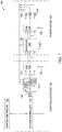
- a modular converter system 100 can control a system of parallel modular inverters 125 (also “inverter modules,” “inverter units”) to drive multiple and/or different types of AC or DC machines, such as the depicted motors 140 (i.e., motors M1, M2, M3).
- the modular converter system 100 comprises the plurality of inverters 125 that are connected in parallel, each of which is able to be configured to receive any of a plurality of motor control algorithms 115A, 115B, 115C (also “control algorithms,” “algorithms”) embedded in a motor control system 110 via a reconfigurable control switching network (CSN) 120.
- CSN reconfigurable control switching network
- the motor control system 110 may comprise one or more motor controller circuits, each of which is configured to operate one or more motors 140.
- Each of the parallel modular inverters 125 can be configured to drive one or more of the plurality of electrical loads (e.g., AC or DC machines such as motors 140), on the load side via a reconfigurable power switching network (PSN) 130.
- PSN reconfigurable power switching network
- each of the parallel modular inverters 125 provides one phase of output power to the electrical loads.
- each of the parallel modular inverters 125 provides multiple phases of output power (e.g., three-phase AC) to the electrical loads.
- the inverter 125A includes three phase legs 210-1, 210-2, 210-3 that are each configured to provide a separate phase output 215 of a three-phase signal 220 to drive selected electrical loads.
- any of the inverters from the plurality of inverters 125 is accessible to drive any one of the electrical loads (such as motors 140) on the load side, and any control algorithm of a plurality of control algorithms 115A, 115B, 115C embedded in the motor control system 110 is accessible to control any of the plurality of inverters 125.
- one or more inverters 125 can drive one motor 140, as necessary to meet load requirements, and/or a plurality of motors 140 on the load side can be driven at the same time, each of which can be driven with one or more inverters 125.
- a plurality of motors 140 on the load side can be driven at the same time with the same motor control algorithm (e.g., 115A) or different motor control algorithms (e.g., some with motor control algorithm 115A, some with motor control algorithm 115B).
- the same motor control algorithm e.g., 115A
- different motor control algorithms e.g., some with motor control algorithm 115A, some with motor control algorithm 115B.
- the system 100 comprises a system controller 105 configured to communicate with a vehicle controller 102 to obtain operational commands from the vehicle controller 102 and to provide status signals for modular converter system 100 and/or other information to the vehicle controller 102.
- the system controller 105 can also reconfigure the power switching network 130 to provide an appropriate number of inverter modules 125 in parallel to drive a motor 140 in real time. In other words, when the load from a motor 140 is increased, the system controller 105 can signal the power switching network 130 to place more inverters 125 in parallel. Conversely, when motor load is decreased, the system controller 105 can signal the power switching network 130 to disengage one or more inverters 125. If necessary, the system controller 105 can then place them in parallel with other inverters 125 to drive other loads.
- the system controller 105 can also reconfigure the control switching network 120 using CSN control signals 122 to provide appropriate motor control algorithms 115A, 115B, 115C as motor control signals 117 to one or more of the inverters 125 driving one or more motor types.
- the inverters 125 may further provide feedback signals 127, such as current and/or voltage values, to the motor control system 110 and the selected motor control algorithm 115A, 115B, 115C.
- motor control algorithms 115A, 115B, 115C provided by system controller 105 include field-oriented control (FOC), direct torque control (DTC), and voltage over frequency control (V/F).
- a typical aircraft can include a starter motor-generator for the main engines (a PM-type motor), a ram-air fan (induction motor), an environmental control system (ECS) compressor motor (PM-type motor), and one or more synchronous motors, all of which may have different power requirements.
- a starter motor-generator for the main engines a PM-type motor
- a ram-air fan induction motor
- an environmental control system (ECS) compressor motor PM-type motor
- system controller 105 can also send, for example and not limitation, motor speed, torque, or power reference values to corresponding motors 140 (e.g., via the motor control system 110).
- system controller 105 can be stored and run on an embedded controller.
- the system controller 105 can comprise, for example and not limitation, a microcontroller, processor, field-programmable gate array (FPGA), or application-specific integrated circuit (ASIC).
- the system controller 105 can use a real-time simulator/emulator or can be run in real-time.
- the number of motor controller algorithms 115A, 115B, 115C can be determined by the number of different motor loads. For example, if the system 100 has three different types of motors 140 to drive, then three motor controller algorithms 115A, 115B, 115C can be developed, with each motor control algorithm 115A, 115B, 115C specific to the motor 140. In another example, if all three motors 140 perform the same function, it is possible that all three loads can be powered using a single motor control algorithm 115A, 115B, or 115C.
- the control switching network 120 can dynamically configure one or more inverters 125, each of which can be driven by a specific control algorithm 115A, 115B, 115C, or a common control algorithm 115A, 115B, 115C, which is routed through control switching network 120 according to CSN control signals 122 provided by the system controller 105.
- a time delay between signals into and out of control switching network 120 can be minimized to improve motor drive performance.
- the control switching network 120 can have a software-based or hardware-based implementation.
- a software-coded control switching network 120 can be run on, for example and not limitation, an embedded controller, real-time simulator, or computer.
- the control switching network 120 can be implemented using a hardware device such as, for example and not limitation, complex programmable logic devices (CPLDs), ASICs, or FPGAs.
- CPLDs complex programmable logic devices
- ASICs application specific integrated circuitry
- the power switching network 130 can be dynamically configured, using PSN control signals 132 from the system controller 105, to connect one or more inverters 125 to drive one or more motors 140 per one or more specific control algorithms 115A, 115B, 115C from the motor control system 110.
- the power switching network 130 can act as a short circuit and/or over-current protection device. In this case, power switch(es) 130 that are associated with the short circuited or over-current load open when a fault is detected.
- the power switching network 130 can be implemented using power switches 225, some non-limiting examples of which including solid state relays, mechanical relays, transistors, and other controllable power switches.
- the system controller 105 controls each power switch 225 using control signals 132.
- the inverters 125 convert DC power (i.e., VDC in Figure 1 ) to the requested AC power output (e.g., with different voltage levels, frequencies, waveforms, etc.) to drive various AC machines (e.g., motors 140) per the selected motor algorithm 115A, 115B, 115C and system controller 105.
- the inverters 125 can comprise, for example and not limitation, insulated-gate bipolar transistors (IGBTs), metal-oxide-semiconductor field-effect transistors (MOSFETs), and bipolar junction transistors (BJTs).
- IGBTs insulated-gate bipolar transistors
- MOSFETs metal-oxide-semiconductor field-effect transistors
- BJTs
- the control switching network 120 includes sufficient numbers of control switches 205 so that each motor control algorithm 115A, 115B, 115C can be selectively and dynamically connected with any one or more of the inverters 125 (i.e., inverters 125A, 125B, 125C, 125D, and/or 125E).
- inverters 125 i.e., inverters 125A, 125B, 125C, 125D, and/or 125E.
- certain combinations of inverters 125 and motor control algorithms 115A, 115B, 115C may be omitted as being not required or not feasible, which can reduce the number of control switches included in control switching network 120.
- the power switching network 130 includes sufficient numbers of power switches 225 so that each of the inverters 125 can be selectively and dynamically connected with any one or more of the electrical loads (i.e., motors 140). Similarly, in other examples, certain combinations of inverters 125 and electrical loads may be omitted to reduce the number of power switches 225 included in power switching network 130. While fifteen (15) control switches 205 (corresponding to three motor control algorithms 115 and five inverters 125) and fifteen (15) power switches 225 (corresponding to the five inverters 125 and three electrical loads) are depicted, these numbers may vary based on the implementation. For example, the number of paralleled inverters 125 can be more than five, such as any suitable number N.
- the dimension of the control switching network 120 will be 3xN, and the dimension of the power switching network 130 will be Nx3.
- the number of motors (or loads) 140 may be more than three, e.g., a number M. Consequently, the dimension of the power switching network will be NxM.
- the modular converter system 100 is divided into a plurality of stages.
- the modular converter system 100 includes a controller stage 145 and a power stage 150.
- the components within the controller stage 145 e.g., system controller 105, motor control system 110
- the controller stage 145 may be powered at a relatively low voltage (e.g., between about 1 volt (V) and 20 V) that is suitable for operating the controller stage components, while the power stage 150 is powered with relatively higher voltages (e.g., between about 100 V to 1000 V or more) suitable for producing the output power required to drive the loads (such as motors 140).
- the power stage 150 is configured to provide a power output having multiple phases (e.g., a three-phase AC output) for driving the loads.
- each connection between inverters 125, power switching network 130, and motors 140 may represent a three-phase power connection.
- the components of controller stage 145 need not be dimensioned to handle the higher voltages and/or currents of the power stage 150.
- the controller stage 145 may generally include smaller and/or less lossy components, reducing the weight and improving the efficiency of the modular converter system 100.
- Control and/or feedback signals communicated between the controller stage 145 and power stage 150 may cross an isolation barrier configured to prevent the higher voltages (e.g., large DC voltages) of the power stage 150 from affecting the lower-voltage components of the controller stage 145.
- the system controller 105 communicates control signals 107 with the motor control system 110 to select particular motor control algorithms 115.
- the motor control system 110 provides selected algorithm(s) as motor control signals 117 that are transmitted via selected path(s) within the control switching network 120 and delivered to the inverters 125.
- the motors 140 provide one or more motor feedback signals 142 to the motor control algorithms 115 for updated control.
- Some non-limiting examples of motor feedback signals 142 include current, voltage, speed, and position values.
- the modular converter system 100 can assign loads based on a load priority factor. In other words, if, for example, the number of loads requested by external aircraft systems (i.e., by vehicle controller 102) is larger than can be provided by the modular converter system 100, the modular converter system 100 can assign loads by a load priority factor, with higher-priority loads being powered before lower-priority loads. If the aircraft (through vehicle controller 102) makes a request for a relatively large load, e.g., for lowering a landing gear, the system 100 can temporarily reassign some or all of the inverters 125 to power the motor(s) 140 associated with the landing gear.
- the modular converter system 100 can reassign the inverters 125 to their previous loads (or to new existing loads). For example, the cabin fan can be temporarily deactivated in favor of lowering the landing gear, and the cabin fan is restarted when the landing gear is down.
- the modular converter system 100 may power some or all of the loads at a reduced setting. In this manner, all loads are powered, but may operate at a lower speed or capacity. So, for example, the aircraft cabin fans, lighting, and entertainment system may request power at the same time in excess of the modular converter system 100 rating. As a result, the modular converter system 100 can, for example, provide full power to the entertainment system, but slightly reduce cabin fan speeds and lighting intensity to reduce overall power demand.
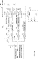
- Figure 3A illustrates an arrangement of converter circuitry within a phase leg of a modular inverter, according to one example.
- arrangement 300 represents a modular inverter 125 that provides a single-phase power output.
- the arrangement 300 represents a phase leg 210 of a modular inverter 125 configured to be connected in parallel with phase legs 210 of other inverters 125.
- Figure 3A provides a detailed illustration of sensing and control circuitry 302 relating to a single inverter or a single inverter phase leg 210, the person of ordinary skill will understand that multiple copies of the circuitry may be provided based on the implementation of the modular converter system.
- each of the five inverters 125A-125E includes three respective phase legs 210-1, 210-2, and 210-3, resulting in a total of fifteen copies of the control circuitry 302 in Figure 3A .
- arrangement 300 includes a plurality of paralleled inverters 125A, 125B which are configured by the power switching network to provide power to a common load.
- the modular inverter 125 includes control circuitry 302 coupled with the system controller 105 and configured to operate the switches 330-1, 330-2 (also "switching elements" 330) of the inverter 304.
- the switches 330-1, 330-2 have a phase output node 340 coupled therebetween.
- the switches 330-1, 330-2 may have any suitable implementation, such as insulated gate bipolar transistors (IGBTs), metal-oxide-semiconductor field-effect transistors (MOSFETs), bipolar junction transistors (BJTs), and so forth.
- the phase output node 340 carries a power output 215.
- a power supply 342 provides the power used to generate the power output 215, and inverter 304 controls the waveform of power output 215 according to the switch timing dictated by the drive signals 326-1, 326-2.
- the power supply 342 provides reference voltages VDC+, VDC- to inverter 304, which as shown correspond to predetermined voltages Vs and -Vs with a ground potential between them. Other configurations of the power supply 342 are possible, such as VDC- at a ground potential.
- the switching elements 330-1, 330-2 may be designed to have a predetermined relative switching strength or other relative switching properties, but during operation may behave slightly differently than designed due to manufacturing tolerances, the presence of parasitic elements based on nearby components, and so forth.
- the switches 330-1, 330-2 can differ in operation from each other, and/or can differ from the desired result of the drive signals 326-1, 326-2 provided by the gate drivers 325-1, 325-2.
- the system controller 105 provides control signals 107, which are used to select motor control algorithms (not shown; 115A, 115B, 115C of Figures 1 , 2 ) to provide motor control signals 117A, 117B, to control circuitry 302 to control the modular inverter 125.
- motor control algorithms not shown; 115A, 115B, 115C of Figures 1 , 2
- isolation barriers 315 are located along each path for motor control signals 117A, 117B.
- the isolation barriers 315 may have any suitable implementation for galvanic isolation, such as class X or class Y capacitors.
- Control circuitry 302 also includes protection logic 320 located between isolation barriers 315 and gate drivers 325-1, 325-2, which may have any suitable implementation for protecting loads during particular operational conditions, such as including short circuit detection logic, overload detection logic, overtemperature detection logic, etc. implemented in hardware and/or software. If any of these operational conditions are detected, the protection logic 320 interrupts the delivery of particular motor control signal(s) 117A and/or 117B to the gate driver(s) 325-1, 325-2 to prevent excessive wear or damage to the connected load.
- the motor control signals 117A and 117B are provided as respective control signals 345A, 345B to the gate drivers 325-1, 325-2.
- the gate drivers 325-1, 325-2 Based on the control signals 345A, 345B, the gate drivers 325-1, 325-2 generate drive signals 326-1, 326-2 for the switches 330-1, 330-2 to provide a desired waveform of the power output 215.
- the power output 215 is provided as a pulse-width modulation (PWM) waveform for driving the load.
- PWM pulse-width modulation
- Control circuitry 302 includes one or more integrators 335-1, 335-2 that are coupled with phase output node 340 and with a reference voltage.
- the integrators 335-1, 335-2 are analog integrators (e.g., an op-amp integrator) configured to provide a continuous sampling of the voltages on phase output node 340. While use of other types of integrators is possible, analog integrators generally provide several advantages over digital integrators. Digital integrators can be more complex and/or expensive to integrate within the arrangement 300. Detecting duty cycle differences between different inverters 125, which can be on the order of a fraction of a percent of the on-time of a switch, requires a large number of samples.
- suitable sampling of a power output 215 in the tens or hundreds of kilohertz (kHz), which is not uncommon for pulse width modulation (PWM) implementations, can require a sampling frequency well into the megahertz (MHz) range.
- An analog integrator by comparison, provides a time-continuous integration of the power output 215 with increased fidelity and resolution.
- the analog integrator also provides a single analog value across the isolation boundary 315 to the system controller 105, reducing bandwidth requirements.
- integrator 335-1 is connected with phase output node 340 and VDC+
- integrator 335-2 is connected with phase output node 340 and VDC-.
- Each of the integrators 335-1, 335-2 are configured to integrate over one or more switching cycles of the drive signals 326-1, 326-2, and to transmit the output signal across an isolation barrier 315 to the system controller 105.
- the system controller 105 includes an analog-to-digital converter (ADC) 305 configured to convert the output signals from integrators 335-1, 335-2 into corresponding discrete values.
- ADC analog-to-digital converter
- the values corresponding to different switches 330 may be compared by the system controller 105 against each other and/or against the desired result of the drive signals 326-1, 326-2 to determine whether the switches 330 are operating as intended or with some error.
- the system controller 105 calculates an applied volt-seconds value 312 corresponding to each switch 330-1, 330-2.
- gate driver 325-1 provides drive signal 326-1 to switch 330-1 that is configured to apply 1000 volts (V) to output node 340 for a one (1) millisecond (ms) duration - a desired applied volt-seconds value of 1.000 V-s.
- the system controller 105 is further configured to calculate one or more gate driver offsets 310 based on the determined error.
- the gate driver offsets 310 may have any suitable form for adjusting the timing (or duty cycle) of the drive signal 326-1. Applying the calculated gate driver offset(s) 310 to gate driver 325-1 adjusts the associated timing of switch 330-1 and reduces or eliminates the error between the desired applied volt-seconds and actual applied volt-seconds values.
- the system controller applies a gate driver offset 310 to control signals 107, which in turn affects control signal 345A and causes switch 330-1 to reduce its duty cycle so that the calculated applied volt-seconds value 312 actually applied to switch 330-1 is the desired 1.000 V-s,
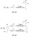
- Figures 3B and 3C illustrate alternate arrangements of integrators within a modular converter system.
- the arrangement 300 of Figure 3A depicts inverter 125 as including a first integrator 335-1 connected with phase output node 340 and a first voltage rail (VDC+), and a second integrator 335-2 connected with phase output node 340 and a second voltage rail (VDC-).
- Arrangement 350 ( Figure 3B ) includes a single integrator 335 for the inverter 125, and the integrator 335 is configured to measure voltages on phase output node 340 that are referenced to a ground potential.
- Arrangement 355 ( Figure 3C ) includes multiple integrators 335A, 335B configured to measure voltages on phase output node 340 that are referenced to a ground potential.
- the measurements of integrators 335A, 335B may be selectively provided to the ADC 305 using a switching arrangement such as a multiplexer 360.
- the select signal 365 may be provided by the system controller 105 (not shown). In some examples, measurements may be provided in an alternating pattern from the integrators 335A, 335B to provide increased accuracy.
- each of the integrators 335-1, 335-2 is configured to integrate over one or more switching cycles of the drive signals 326-1, 326-2.
- the measurements performed by the integrators 335-1, 335-2 may be periodically reset using a reset signal provided to the integrators 335-1, 335-2.
- control signals 345A, 345B to the gate drivers 325-1, 325-2 can provide a suitable reset signal.
- a rising edge of control signals 345A, 345B can indicate the completion of a particular switching cycle and may be used to trigger a reset of the integrators 335-1, 335-2.
- the system controller 105 may generate a distinct reset signal (not shown) for the integrators 335-1, 335-2.
- Resetting the integrators 335-1, 335-2 is generally not an instantaneous event.
- resetting the integrator may comprise closing a switch to cause discharge of the feedback capacitor according to an associated time constant. Therefore, during some time periods the integrators 335-1, 335-2 are not integrating voltage values of the phase output node 340, which can have effects on resulting measurements.
- Arrangement 355 ( Figure 3C ) provides one means for improving measurement accuracy.
- a reset of a first integrator 335A controlled by a first reset signal i.e., RESET 1
- the ADC 305 receives measurements from the second, non-resetting integrator 335B to more completely capture the voltage values of the phase output node 340.
- the ADC 305 receives measurements from the first, non-resetting integrator 335A.
- the select signal 365 controlling the multiplexer 360 may be a separate signal provided from the system controller 105 (not shown) or may be based on a logic combination of the first and/or second reset signals.
- the system controller 105 may perform a mathematical extrapolation for measurement(s) of ADC 305 corresponding to reset periods.
- This approach may be feasible where electromagnetic interference (EMI) cross-talk, such as noise introduced by other switching elements of the arrangement 300, 350, 355, is controlled relatively well.
- EMI electromagnetic interference
- the system controller 105 and ADC 305 are located on the "power side" of the isolation boundary 315 (i.e., with the gate drivers 325-1, 325-2 and the switches 330-1, 330-2). Such an implementation would generally require an increased bandwidth across the isolation boundary 315, as the system controller 105 may still be required to communicate with an external vehicle controller and/or other control elements in a different power supply regime.
- fast control loops may be provided between the gate drivers 325-1, 325-2 and the voltage measurements taken at the phase output node 340A, which in some cases may be used to implement the gate driver offsets 310 instead of the system controller 105.
- the system controller 105 provides the gate driver offsets 310 and the fast control loops provide adjustments to the drive signals 326-1, 326-2 that are relatively small compared to the gate driver offsets 310.
- Figure 3D illustrates an arrangement 375 of a plurality of inverters within a multi-phase modular converter system, according to one example. More specifically, arrangement 375 illustrates that similar techniques to those discussed above for adjusting operation of gate drivers for modular inverters may be used to balance current production between inverter modules of a multi-phase modular converter system.
- Inverter units 125A and 125B are similarly configured, each having three phase legs with three phase output nodes 340.
- inverter units 125C-125E are also similarly configured for three-phase operation.
- phase output nodes 340-1 and 340-4 are coupled together (as well as with phase output nodes of inverter units 125C-125E) to produce a power output 215-1 having a first phase.
- the phase leg 210-1 and 210-4 are connected in parallel.
- Phase output nodes 340-2 and 340-5 are coupled together (again, with phase output nodes of inverter units 125C-125E) to produce power output 215-2 having a second phase.
- Phase output nodes 340-3 and 340-6 are coupled together (again, with phase output nodes of inverter units 125C-125E) to produce power output 215-3 having a third phase.
- each of the inverters 304 of the inverter units 125A-125E may behave slightly differently during operation due to manufacturing tolerances, the presence of parasitic elements based on nearby components, and so forth.
- the inverters 304 can differ in operation from each other, and/or can differ from the desired result of the drive signals provided to the inverters 304 by control circuitry 302.
- control circuitry 302 included in each phase leg 210 samples voltages on the corresponding phase output node 340, and communicates these voltages with the system controller 105.
- the system controller 105 may calculate applied volt-seconds values for each of the phase output nodes 340, which may then be compared to determine whether any of the inverters 125A-125E have uneven loading.
- the system controller 105 may also generate one or more gate driver offsets to control subsequent operation of the inverters 304 to mitigate any uneven loading and/or error between desired applied volt-seconds values and the values actually applied by the inverters 304.
- the system controller 105 sends control signals to paralleled phase legs 210-1, 210-4 that are configured to cause corresponding inverters 304 to apply 1000 V to output nodes 340-1, 340-4 for a 1 ms duration (i.e., a desired value of 1.000 V-s). Due to tolerances and/or parasitic elements for the inverters 304, say the applied volt-seconds values calculated by the system controller 105 are 1.001 V-s to phase leg 210-1 and 0.999 V-s to phase leg 210-4.
- the system controller 105 applies a calculated gate driver offset to phase leg 210-1 to reduce the duty cycle of the corresponding inverter to match the 0.999 V-s value for phase leg 210-4.
- the system controller 105 applies a calculated gate driver offset to phase leg 210-4 to apply the 1000V for a longer period and match the 1.001 V-s value for phase leg 210-1.
- the system controller 105 applies gate driver offsets to both phase legs 210-1, 210-4 to balance the output from the inverters and to correct the differences between the calculated applied volt-seconds values (i.e., 1.001 V-s, 0.999 V-s) and the desired result of the drive signals (i.e., 1.000 V-s).
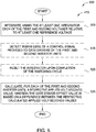
- Figure 4 illustrates a method of controlling power output of a modular converter system comprising a plurality of parallel inverter units, according to one example.
- method 400 may be performed consistent with any of the examples of modular converter system 100, 200 and arrangements 300, 350, 355, 375 discussed above.
- Method 400 begins at block 405, where switching elements of first and second inverter units are driven with initial drive signals to produce an in-phase power output.
- the first and second inverter units may each include different phase legs that are paralleled together using a power switching network. Driving the signals may be performed by gate drivers of the first and second inverter units.
- the initial drive signals for the first inverter unit and the second inverter unit are the same, but this is not a requirement.
- a gate driver offset value is determined based on respective first and second voltages at first and second phase output nodes of the respective first and second inverter units. Determining the gate driver offset value may be determined by a system controller coupled with the first and second inverter units, or alternately by one or more local fast control loops coupled with the gate drivers and the phase output nodes.
- determining the gate driver offset value comprises integrating, using at least one integrator coupled with each of the first and second phase output nodes, each of the first and second voltages relative to at least one reference voltage. In some examples, determining the gate driver offset value comprises calculating, for each of the first and second inverter units, a respective applied volt-seconds value. The gate driver offset value is based on a difference between the respective calculated applied volt-seconds values, which indicates an imbalance of the loading between the first and second inverter units. The gate driver offset value may be further based on a difference between the calculated applied volt-seconds values and the desired result of the drive signals.
- the switching elements of the first and second inverter units are driven with subsequent drive signals, such that the respective amounts of current provided by the first and second inverter units when producing the in-phase power output are balanced.
- the subsequent drive signals for one or both of the first and second inverter units may be adjusted using the determined gate driver offset value.
- the subsequent drive signals may also cause the first and second inverter units to produce the desired result of the drive signals.
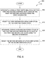
- FIGS. 5 and 6 illustrate methods of determining a gate driver offset value, according to one example.
- Each of methods 500 and 600 represent a possible implementation of block 415 of method 400, in which a gate driver offset value is determined based on respective first and second voltages at first and second phase output nodes of respective first and second inverter units.
- Method 500 begins at block 505, where the at least one integrator coupled with the first and second phase output nodes integrates each of the first and second voltages relative to at least one reference voltage.
- the reference voltages may be voltage rails configured to power the inverter units.
- a rising edge is detected for a control signal provided to gate drivers of the first and second inverter units.
- the integrator is reset upon completion of the switching cycle, which is indicated by the detected rising edge.
- a falling edge of the control signal may be used, or a separate control signal configured to reset the integrator.
- the system controller calculates, for each of the first and second inverter units, a respective applied volt-seconds values.
- the gate driver offset values is based on a difference between the respective calculated applied volt-seconds values.
- Method 600 generally applies to an implementation having multiple integrators connected with a particular phase output node, such as shown in Figure 3C .
- the phase output node of the first inverter unit may have a first pair of integrators
- the phase output node of the second inverter unit may have a second pair of integrators.
- Method 600 begins at block 605, where during a first switching cycle of the first and second inverter units, a first integrator integrates each of the first and second voltages.
- the first integrator is reset upon completion of the first switching cycle, e.g., based on a detected rising or falling edge of a control signal.
- a second integrator integrates each of the first and second voltages.
- Blocks 615 and 625 may be at least partly overlapping in time, such that measurement of the voltages can be substantially continuous despite the occasional resetting of the first integrator.
- the second integrator is reset upon completion of the second switching cycle.
- Method 600 ends following completion of block 635.
- method 600 repeats, returning from block 635 to block 605.
- blocks 635 and 605 may be at least partly overlapping in time.
- aspects of the present disclosure may be embodied as a system, method, or computer program product. Accordingly, aspects of the present disclosure may take the form of an entirely hardware example, an entirely software example (including firmware, resident software, micro-code, etc.) or an example combining software and hardware aspects that may all generally be referred to herein as a "circuit," "module” or “system.” Furthermore, aspects of the present disclosure may take the form of a computer program product embodied in one or more computer readable medium(s) having computer readable program code embodied thereon.
- the computer readable medium may be a computer readable signal medium or a computer readable storage medium.
- a computer readable storage medium may be, for example, but not limited to, an electronic, magnetic, optical, electromagnetic, infrared, or semiconductor system, apparatus, or device, or any suitable combination of the foregoing.
- a computer readable storage medium may be any tangible medium that can contain, or store a program for use by or in connection with an instruction execution system, apparatus, or device.
- a computer readable signal medium may include a propagated data signal with computer readable program code embodied therein, for example, in baseband or as part of a carrier wave. Such a propagated signal may take any of a variety of forms, including, but not limited to, electro-magnetic, optical, or any suitable combination thereof.
- a computer readable signal medium may be any computer readable medium that is not a computer readable storage medium and that can communicate, propagate, or transport a program for use by or in connection with an instruction execution system, apparatus, or device.
- Program code embodied on a computer readable medium may be transmitted using any appropriate medium, including but not limited to wireless, wireline, optical fiber cable, RF, etc., or any suitable combination of the foregoing.
- Computer program code for carrying out operations for aspects of the present disclosure may be written in any combination of one or more programming languages, including an object oriented programming language such as Java, Smalltalk, C++ or the like and conventional procedural programming languages, such as the "C" programming language or similar programming languages.
- the program code may execute entirely on the user's computer, partly on the user's computer, as a stand-alone software package, partly on the user's computer and partly on a remote computer or entirely on the remote computer or server.
- the remote computer may be connected to the user's computer through any type of network, including a local area network (LAN) or a wide area network (WAN), or the connection may be made to an external computer (for example, through the Internet using an Internet Service Provider).
- LAN local area network
- WAN wide area network
- Internet Service Provider for example, AT&T, MCI, Sprint, EarthLink, MSN, GTE, etc.
- These computer program instructions may also be stored in a computer readable medium that can direct a computer, other programmable data processing apparatus, or other devices to function in a particular manner, such that the instructions stored in the computer readable medium produce an article of manufacture including instructions which implement the function/act specified in the flowchart and/or block diagram block or blocks.
- the computer program instructions may also be loaded onto a computer, other programmable data processing apparatus, or other devices to cause a series of operational steps to be performed on the computer, other programmable apparatus or other devices to produce a computer implemented process such that the instructions which execute on the computer or other programmable apparatus provide processes for implementing the functions/acts specified in the flowchart and/or block diagram block or blocks.
- each block in the flowchart or block diagrams may represent a module, segment, or portion of instructions, which comprises one or more executable instructions for implementing the specified logical function(s).
- the functions noted in the block may occur out of the order noted in the figures.
- two blocks shown in succession may, in fact, be executed substantially concurrently, or the blocks may sometimes be executed in the reverse order, depending upon the functionality involved.
- determining the gate driver offset value comprises: calculating (535), for each of the first and second inverter units, a respective applied volt-seconds value (312), wherein the gate driver offset value is based on a difference between the respective calculated applied volt-seconds values.
- each of the first and second phase output nodes are coupled with at least one integrator (335-1, 335-2) of the modular converter system, wherein determining the gate driver offset value comprises: integrating (505), using the at least one integrator, each of the first and second voltages relative to at least one reference voltage (VDC+, VDC-).
- the method wherein the at least one reference voltage comprises a system ground.
- the method wherein integrating each of the first and second voltages occurs during a switching cycle of the first and second inverter units, the method further comprising: resetting (525) the integrator upon completion of the switching cycle.
- the method wherein resetting of the integrator occurs upon detecting (515) a rising edge of a control signal (345A, 345B) provided to gate drivers of the first and second inverter units.
- the method wherein the at least one integrator comprises first and second integrators (335A, 335B), the method further comprising: integrating (605), during a first switching cycle of the first and second inverter units, each of the first and second voltages using the first integrator; and integrating (625), during a second switching cycle of the first and second inverter units, each of the first and second voltages using the second integrator.
- a modular converter system comprising: a system controller (105); and at least first and second inverter units (125A, 125B) connected in parallel and configured to produce an in-phase power output (215-1, 215-2, 215-3), each inverter unit of the first and second inverter units respectively comprising: a pair of switching elements (330-1, 330-2) having a phase output node (340) coupled therebetween, and a pair of gate drivers (325-1, 325-2), each gate driver configured to receive a respective control signal (345A, 345B) from the system controller and to generate a drive signal (326-1, 326-2) to control switching of a respective one of the pair of switching elements, wherein the system controller is configured to: determine a gate driver offset value (310) based on respective voltages at the phase output nodes of the first and second inverter units, and control, based on the determined gate driver offset value, the gate drivers using first and second inverter units with subsequent drive signals (326-1, 326-2) such that the amounts of current provided
- the modular converter system wherein the system controller is further configured to calculate, for each of the first and second inverter units, a respective applied volt-seconds value (312), wherein the gate driver offset value is based on a difference between the respective calculated applied volt-seconds values.
- the modular converter system further comprising:
- the modular converter system wherein the at least one reference voltage comprises a system ground.
- the modular converter system wherein integrating each of the first and second voltages occurs during a switching cycle of the first and second inverter units, wherein the system controller is further configured to reset the one or more first integrators and the one or more second integrators upon completion of the switching cycle.
- the modular converter system wherein resetting the one or more first integrators and the one or more second integrators occurs upon detecting a rising edge of a control signal (345A, 345B) provided to the pair of gate drivers of each of the first and second inverter units.
- the modular converter system wherein the one or more first integrators comprise a first plurality of integrators (335A, 335B) and the one or more second integrators comprise a second plurality of integrators (335A, 335B), wherein at least one integrator of each of the first plurality and the second plurality of integrators is configured to integrate the respective first and second voltages during a first switching cycle of the first and second inverter units, and wherein at least another integrator of each of the first plurality and the second plurality of integrators is configured to integrate the respective first and second voltages during a second switching cycle of the first and second inverter units.
- a non-transitory computer-readable medium comprising computer program code that, when executed by operation of one or more computer processors, performs an operation of controlling power output of a modular converter system (100, 200) comprising a plurality of parallel inverter units (125), the plurality of parallel inverter units comprising a first inverter unit (125A) with at least a first phase output node (340-1) and a second inverter unit (125B) with at least a second phase output node (340-4), the operation comprising: communicating with a plurality of gate drivers (325-1, 325-2) to drive (405) switching elements (330-1, 330-2) of the first and second inverter units with initial drive signals (326-1, 326-2) to produce an in-phase power output (215-1); determining (415) a gate driver offset value (310) based on respective first and second voltages at the first and second phase output nodes; and communicating with the plurality of gate drivers to drive (425), based on the determined gate driver offset value, the switching elements of the
- determining the gate driver offset value comprises: calculating (535), for each of the first and second inverter units, a respective applied volt-seconds value (312), wherein the gate driver offset value is based on a difference between the respective calculated applied volt-seconds values.
- each of the first and second phase output nodes are coupled with at least one integrator (335-1, 335-2) of the modular converter system, wherein determining the gate driver offset value comprises: integrating (505), using the at least one integrator, each of the first and second voltages relative to at least one reference voltage (VDC+, VDC-).
- the computer-readable medium wherein integrating each of the first and second voltages occurs during a switching cycle of the first and second inverter units, the operation further comprising: resetting (525) the integrator upon completion of the switching cycle.
- the computer-readable medium wherein resetting of the integrator occurs upon detecting (515) a rising edge of a control signal (345A, 345B) provided to gate drivers of the first and second inverter units.
- the computer-readable medium wherein the at least one integrator comprises first and second integrators (335A, 335B), the operation further comprising: integrating (605), during a first switching cycle of the first and second inverter units, each of the first and second voltages using the first integrator; and integrating (625), during a second switching cycle of the first and second inverter units, each of the first and second voltages using the second integrator.
Landscapes
- Engineering & Computer Science (AREA)
- Power Engineering (AREA)
- Inverter Devices (AREA)
- Supply And Distribution Of Alternating Current (AREA)
Applications Claiming Priority (1)
| Application Number | Priority Date | Filing Date | Title |
|---|---|---|---|
| US15/055,828 US9991778B2 (en) | 2016-02-29 | 2016-02-29 | Balancing current within a modular converter system |
Publications (2)
| Publication Number | Publication Date |
|---|---|
| EP3211785A1 EP3211785A1 (en) | 2017-08-30 |
| EP3211785B1 true EP3211785B1 (en) | 2019-09-25 |
Family
ID=58464135
Family Applications (1)
| Application Number | Title | Priority Date | Filing Date |
|---|---|---|---|
| EP17157979.0A Active EP3211785B1 (en) | 2016-02-29 | 2017-02-24 | Balancing current within a modular converter system |
Country Status (8)
| Country | Link |
|---|---|
| US (1) | US9991778B2 (zh) |
| EP (1) | EP3211785B1 (zh) |
| JP (1) | JP6872928B2 (zh) |
| KR (1) | KR102614306B1 (zh) |
| CN (1) | CN107134941B (zh) |
| BR (1) | BR102016030695B1 (zh) |
| CA (1) | CA2949637C (zh) |
| RU (1) | RU2724468C2 (zh) |
Families Citing this family (12)
| Publication number | Priority date | Publication date | Assignee | Title |
|---|---|---|---|---|
| US10396673B1 (en) * | 2017-06-05 | 2019-08-27 | Maxim Integrated Products, Inc. | DC-to-DC converter controllers, DC-to-DC converters, and associated methods |
| CN109229361A (zh) * | 2017-07-11 | 2019-01-18 | 深圳市道通智能航空技术有限公司 | 电机控制系统及无人机 |
| US10554149B2 (en) * | 2017-11-20 | 2020-02-04 | Solaredge Technologies Ltd. | Providing positional awareness information and increasing power quality of parallel connected inverters |
| US10333436B2 (en) | 2017-11-29 | 2019-06-25 | Regal Beloit America, Inc. | Drive circuit for electric motors |
| US10554157B2 (en) | 2017-11-29 | 2020-02-04 | Regal Beloit America, Inc. | Drive circuit for electric motors |
| JP2019161714A (ja) * | 2018-03-08 | 2019-09-19 | 株式会社東芝 | モータ制御装置およびプログラム |
| FR3078845B1 (fr) | 2018-03-08 | 2022-08-05 | Thales Sa | Architecture electrique de pilotage de convertisseurs et aeronef comprenant l'architecture |
| UA130255U (uk) * | 2018-06-23 | 2018-11-26 | Дмитро Валерійович Хачатуров | Модульний високовольтний електротехнічний пристрій |
| KR102086530B1 (ko) * | 2018-11-14 | 2020-03-09 | 한국전기연구원 | 모듈러 멀티레벨 컨버터 서브모듈의 커패시터 전압 조정 방법 및 상기 방법을 실행시키기 위한 컴퓨터 판독 가능한 프로그램을 기록한 기록 매체 |
| CN110518859B (zh) * | 2019-08-14 | 2021-05-25 | 江苏大学 | 一种基于扰动观测器的五相永磁电机短路容错直接转矩控制方法 |
| US11300986B2 (en) | 2020-02-25 | 2022-04-12 | Hamilton Sundstrand Corporation | Current balancing |
| CN111817610B (zh) * | 2020-06-03 | 2021-11-02 | 中国人民解放军海军工程大学 | 用于电机驱动能源复用的电机选通装置及工作方法 |
Family Cites Families (52)
| Publication number | Priority date | Publication date | Assignee | Title |
|---|---|---|---|---|
| JPS62123964A (ja) * | 1985-11-20 | 1987-06-05 | Fuji Electric Co Ltd | 電圧形pwmインバ−タ |
| US4905117A (en) * | 1988-09-02 | 1990-02-27 | Westinghouse Electric Corp. | Circuit and method for DC content protection of parallel VSCF power systems |
| EP0409226A3 (en) | 1989-07-21 | 1993-01-13 | Hitachi, Ltd. | Power supply control system |
| JP2614788B2 (ja) | 1991-04-24 | 1997-05-28 | 株式会社日立製作所 | 交流電動機制御装置 |
| US6792337B2 (en) | 1994-12-30 | 2004-09-14 | Power Measurement Ltd. | Method and system for master slave protocol communication in an intelligent electronic device |
| JPH09331682A (ja) * | 1996-06-12 | 1997-12-22 | Meidensha Corp | 電力変換器 |
| JP3426939B2 (ja) | 1997-10-30 | 2003-07-14 | 株式会社東芝 | 自励式電流形電力変換装置の制御装置 |
| SE0102230L (sv) * | 2001-06-25 | 2002-12-26 | Ragnar Joensson | Switchkrets med multipla steg |
| US7138773B2 (en) | 2003-06-24 | 2006-11-21 | General Electric Company | Multiple inverters for motors |
| JP4271090B2 (ja) * | 2004-06-25 | 2009-06-03 | 東洋電機製造株式会社 | 発電機並列運転用三相インバータ装置 |
| JP4430501B2 (ja) | 2004-09-29 | 2010-03-10 | トヨタ自動車株式会社 | 動力出力装置およびそれを備えた車両 |
| FR2900635B1 (fr) | 2006-05-05 | 2008-07-25 | Hispano Suiza Sa | Systeme d'alimentation et de commande d'equipements electriques d'un moteur d'aeronef ou de son environnement |
| FR2900636B1 (fr) * | 2006-05-05 | 2009-03-06 | Hispano Suiza Sa | Circuit d'alimentation en energie electrique pour des equipements electriques d'un moteur d'aeronef ou de son environnement |
| CN100359779C (zh) * | 2006-05-08 | 2008-01-02 | 浙江大学 | 采用滤波器中间电流反馈的并网逆变器电流控制方法 |
| US20070295545A1 (en) | 2006-05-11 | 2007-12-27 | Romig Bernard E | Differential Steering and Traction Control For Electrically Propelled Mower |
| JP4792553B2 (ja) * | 2006-08-29 | 2011-10-12 | 富士電機株式会社 | 並列運転インバータの電圧補正方法とその回路 |
| FR2907760B1 (fr) | 2006-10-25 | 2009-06-12 | Airbus France Sas | Systeme et procede d'alimentation en puissance a bord d'un aeronef. |
| US7615892B2 (en) | 2006-11-09 | 2009-11-10 | Honeywell International Inc. | Modular and scalable power conversion system for aircraft |
| US8102142B2 (en) | 2007-07-30 | 2012-01-24 | GM Global Technology Operations LLC | Double ended inverter system for a vehicle having two energy sources that exhibit different operating characteristics |
| ES2593471T3 (es) | 2007-12-12 | 2016-12-09 | Foss Maritime Company | Sistemas de propulsión híbridos |
| CN102067428B (zh) * | 2008-06-23 | 2014-04-02 | 爱立信电话股份有限公司 | 同步整流器的驱动电路及其控制方法 |
| US8125164B2 (en) | 2008-07-18 | 2012-02-28 | The Boeing Company | Parallel motor controller architecture |
| FR2941107B1 (fr) * | 2009-01-09 | 2015-08-14 | Hispano Suiza Sa | Systeme electrique de demarrage des moteurs d'un aeronef |
| US8345454B1 (en) * | 2009-11-21 | 2013-01-01 | The Boeing Company | Architecture and control method for dynamically conditioning multiple DC sources to driven an AC load |
| JP2011152027A (ja) | 2009-12-25 | 2011-08-04 | Denso Corp | 電動機駆動装置、および、これを用いた電動パワーステアリング装置 |
| US8223511B2 (en) * | 2010-06-07 | 2012-07-17 | Rockwell Automation Technologies, Inc. | Common mode voltage reduction apparatus and method for current source converter based drive |
| US9106201B1 (en) * | 2010-06-23 | 2015-08-11 | Volterra Semiconductor Corporation | Systems and methods for DC-to-DC converter control |
| US9577424B2 (en) | 2010-07-16 | 2017-02-21 | Rockwell Automation Technologies, Inc. | Parallel motor drive disable verification system and method |
| JP5633631B2 (ja) | 2011-03-16 | 2014-12-03 | トヨタ自動車株式会社 | インバータの過熱保護制御装置およびインバータの過熱保護制御方法 |
| FR2972711B1 (fr) * | 2011-03-17 | 2013-04-19 | Hispano Suiza Sa | Alimentation en energie electrique d'un aeronef |
| CN102110991A (zh) * | 2011-03-31 | 2011-06-29 | 山亿新能源股份有限公司 | 光伏电站中并网逆变器的循环主从群控方法 |
| DE102011002084A1 (de) * | 2011-04-15 | 2012-10-18 | Sma Solar Technology Ag | Verfahren und Vorrichtung zur Bestimmung eines Fehlerstromanteils an einem Differenzstrom |
| WO2014025734A2 (en) | 2012-08-09 | 2014-02-13 | Danfoss Power Electronics A/S | Modular inverter drive |
| CN103856045A (zh) * | 2012-12-04 | 2014-06-11 | 韩山师范学院 | 一种基于分层思想的模糊pi双环控制方法 |
| US9281761B2 (en) * | 2013-01-18 | 2016-03-08 | General Electric Company | Control scheme for current balancing between parallel bridge circuits |
| US9325170B2 (en) | 2013-02-01 | 2016-04-26 | Hamilton Sundstrand Corporation | Matrix-based power distribution architecture |
| US9479084B2 (en) | 2013-02-20 | 2016-10-25 | Infineon Technologies Ag | Pseudo zero vectors for space vector modulation and enhanced space vector modulation |
| US9533638B2 (en) * | 2013-07-18 | 2017-01-03 | The Boeing Company | Aircraft universal power converter |
| CN104467396A (zh) * | 2013-09-24 | 2015-03-25 | 厦门蓝溪科技有限公司 | 一种电源产品数字pfc控制系统 |
| EP3068034B1 (en) | 2013-11-08 | 2022-08-03 | Mitsubishi Electric Corporation | Alternating-current rotating machine controller |
| US9209721B2 (en) * | 2014-04-29 | 2015-12-08 | The Boeing Company | Systems and methods for the control and operation of a parallel motor controller architecture |
| KR101637650B1 (ko) * | 2014-05-20 | 2016-07-20 | 엘지이노텍 주식회사 | 직류-직류 변환기 |
| EP2963800B1 (en) * | 2014-07-02 | 2021-03-24 | Siemens Aktiengesellschaft | Controlling parallel converter systems for wind turbines |
| US9419553B2 (en) * | 2014-07-25 | 2016-08-16 | Denso Corporation | Apparatus for controlling rotary machine |
| US10079493B2 (en) | 2014-09-30 | 2018-09-18 | The Boeing Company | Parallel modular converter architecture |
| US9991719B2 (en) | 2014-09-30 | 2018-06-05 | The Boeing Company | Systems and methods for reducing circulating current and phase to phase imbalance in a parallel modular converter system |
| US9647455B2 (en) | 2014-09-30 | 2017-05-09 | The Boeing Company | EMI filter systems and methods for parallel modular converters |
| US20160118899A1 (en) * | 2014-10-24 | 2016-04-28 | Keithley Instruments, Inc. | Magnetization balancing method |
| US9614461B2 (en) * | 2014-12-02 | 2017-04-04 | Princeton Power Systems, Inc. | Bidirectional high frequency variable speed drive for CHP (combined heating and power) and flywheel applications |
| US9755537B2 (en) | 2015-03-04 | 2017-09-05 | Infineon Technologies Austria Ag | Multi-cell power conversion method with failure detection and multi-cell power converter |
| CN104836430B (zh) * | 2015-05-22 | 2017-09-22 | 国网河南省电力公司电力科学研究院 | 一种应用于双向变换器的电压、电流双环控制的优化方法 |
| CN105356812B (zh) * | 2015-10-23 | 2018-10-02 | 杭州娃哈哈精密机械有限公司 | 永磁同步电机启动电路及启动方法 |
-
2016
- 2016-02-29 US US15/055,828 patent/US9991778B2/en active Active
- 2016-11-23 CA CA2949637A patent/CA2949637C/en active Active
- 2016-11-25 RU RU2016146391A patent/RU2724468C2/ru active
- 2016-11-29 KR KR1020160159995A patent/KR102614306B1/ko active IP Right Grant
- 2016-12-27 BR BR102016030695-7A patent/BR102016030695B1/pt active IP Right Grant
-
2017
- 2017-02-21 JP JP2017029544A patent/JP6872928B2/ja active Active
- 2017-02-24 EP EP17157979.0A patent/EP3211785B1/en active Active
- 2017-02-27 CN CN201710107352.0A patent/CN107134941B/zh active Active
Non-Patent Citations (1)
| Title |
|---|
| None * |
Also Published As
| Publication number | Publication date |
|---|---|
| BR102016030695A2 (pt) | 2017-09-05 |
| EP3211785A1 (en) | 2017-08-30 |
| CA2949637A1 (en) | 2017-08-29 |
| CA2949637C (en) | 2023-09-26 |
| KR102614306B1 (ko) | 2023-12-14 |
| JP6872928B2 (ja) | 2021-05-19 |
| US20170250622A1 (en) | 2017-08-31 |
| CN107134941B (zh) | 2021-06-01 |
| JP2017163826A (ja) | 2017-09-14 |
| BR102016030695B1 (pt) | 2022-11-16 |
| RU2724468C2 (ru) | 2020-06-23 |
| RU2016146391A3 (zh) | 2020-04-16 |
| CN107134941A (zh) | 2017-09-05 |
| RU2016146391A (ru) | 2018-05-25 |
| US9991778B2 (en) | 2018-06-05 |
| KR20170101766A (ko) | 2017-09-06 |
Similar Documents
| Publication | Publication Date | Title |
|---|---|---|
| EP3211785B1 (en) | Balancing current within a modular converter system | |
| US11431176B2 (en) | Parallel modular converter architecture | |
| CN107659195B (zh) | 电流平衡系统及相关方法和计算机可读介质 | |
| US9991719B2 (en) | Systems and methods for reducing circulating current and phase to phase imbalance in a parallel modular converter system | |
| EP3360795A1 (en) | Power distribution control within a modular converter system using efficiency calculations | |
| EP2811633A2 (en) | System and method for reducing reactive current on a common DC bus with multiple inverters | |
| US9586789B2 (en) | Elevator braking in a battery powered elevator system | |
| US20160094030A1 (en) | EMI Filter Systems and Methods For Parallel Modular Converters | |
| JP6356900B2 (ja) | 少なくとも発電機で作動可能な電気機械の作動方法およびその実施手段 | |
| KR101452636B1 (ko) | 인버터 시스템 및 이의 전력 케이블 상태 검출 방법 | |
| US9337767B2 (en) | Single bus star connected reluctance drive and method | |
| WO2019087944A1 (ja) | コンバータ、インバータ装置、電力変換装置および分散電源型のコンベア搬送システム | |
| CA2905116C (en) | Systems and methods for reducing circulating current and phase-to-phase imbalance in a parallel modular converter system | |
| WO2021069895A1 (en) | Method and apparatus for controlling electric motors | |
| JP2011125099A (ja) | インバータの並列運転制御装置 |
Legal Events
| Date | Code | Title | Description |
|---|---|---|---|
| PUAI | Public reference made under article 153(3) epc to a published international application that has entered the european phase |
Free format text: ORIGINAL CODE: 0009012 |
|
| STAA | Information on the status of an ep patent application or granted ep patent |
Free format text: STATUS: REQUEST FOR EXAMINATION WAS MADE |
|
| 17P | Request for examination filed |
Effective date: 20170224 |
|
| AK | Designated contracting states |
Kind code of ref document: A1 Designated state(s): AL AT BE BG CH CY CZ DE DK EE ES FI FR GB GR HR HU IE IS IT LI LT LU LV MC MK MT NL NO PL PT RO RS SE SI SK SM TR |
|
| AX | Request for extension of the european patent |
Extension state: BA ME |
|
| REG | Reference to a national code |
Ref country code: DE Ref legal event code: R079 Ref document number: 602017007230 Country of ref document: DE Free format text: PREVIOUS MAIN CLASS: H02M0007493000 Ipc: H02M0007537000 |
|
| GRAP | Despatch of communication of intention to grant a patent |
Free format text: ORIGINAL CODE: EPIDOSNIGR1 |
|
| STAA | Information on the status of an ep patent application or granted ep patent |
Free format text: STATUS: GRANT OF PATENT IS INTENDED |
|
| RIC1 | Information provided on ipc code assigned before grant |
Ipc: H02M 7/537 20060101AFI20181105BHEP Ipc: H02M 1/088 20060101ALI20181105BHEP Ipc: H02J 1/14 20060101ALI20181105BHEP Ipc: H02M 7/493 20070101ALI20181105BHEP |
|
| INTG | Intention to grant announced |
Effective date: 20181127 |
|
| GRAJ | Information related to disapproval of communication of intention to grant by the applicant or resumption of examination proceedings by the epo deleted |
Free format text: ORIGINAL CODE: EPIDOSDIGR1 |
|
| STAA | Information on the status of an ep patent application or granted ep patent |
Free format text: STATUS: REQUEST FOR EXAMINATION WAS MADE |
|
| GRAP | Despatch of communication of intention to grant a patent |
Free format text: ORIGINAL CODE: EPIDOSNIGR1 |
|
| STAA | Information on the status of an ep patent application or granted ep patent |
Free format text: STATUS: GRANT OF PATENT IS INTENDED |
|
| INTC | Intention to grant announced (deleted) | ||
| INTG | Intention to grant announced |
Effective date: 20190410 |
|
| GRAS | Grant fee paid |
Free format text: ORIGINAL CODE: EPIDOSNIGR3 |
|
| GRAA | (expected) grant |
Free format text: ORIGINAL CODE: 0009210 |
|
| STAA | Information on the status of an ep patent application or granted ep patent |
Free format text: STATUS: THE PATENT HAS BEEN GRANTED |
|
| AK | Designated contracting states |
Kind code of ref document: B1 Designated state(s): AL AT BE BG CH CY CZ DE DK EE ES FI FR GB GR HR HU IE IS IT LI LT LU LV MC MK MT NL NO PL PT RO RS SE SI SK SM TR |
|
| REG | Reference to a national code |
Ref country code: GB Ref legal event code: FG4D |
|
| REG | Reference to a national code |
Ref country code: CH Ref legal event code: EP |
|
| REG | Reference to a national code |
Ref country code: DE Ref legal event code: R096 Ref document number: 602017007230 Country of ref document: DE |
|
| REG | Reference to a national code |
Ref country code: AT Ref legal event code: REF Ref document number: 1184794 Country of ref document: AT Kind code of ref document: T Effective date: 20191015 |
|
| REG | Reference to a national code |
Ref country code: IE Ref legal event code: FG4D |
|
| REG | Reference to a national code |
Ref country code: NL Ref legal event code: MP Effective date: 20190925 |
|
| PG25 | Lapsed in a contracting state [announced via postgrant information from national office to epo] |
Ref country code: NO Free format text: LAPSE BECAUSE OF FAILURE TO SUBMIT A TRANSLATION OF THE DESCRIPTION OR TO PAY THE FEE WITHIN THE PRESCRIBED TIME-LIMIT Effective date: 20191225 Ref country code: HR Free format text: LAPSE BECAUSE OF FAILURE TO SUBMIT A TRANSLATION OF THE DESCRIPTION OR TO PAY THE FEE WITHIN THE PRESCRIBED TIME-LIMIT Effective date: 20190925 Ref country code: FI Free format text: LAPSE BECAUSE OF FAILURE TO SUBMIT A TRANSLATION OF THE DESCRIPTION OR TO PAY THE FEE WITHIN THE PRESCRIBED TIME-LIMIT Effective date: 20190925 Ref country code: SE Free format text: LAPSE BECAUSE OF FAILURE TO SUBMIT A TRANSLATION OF THE DESCRIPTION OR TO PAY THE FEE WITHIN THE PRESCRIBED TIME-LIMIT Effective date: 20190925 Ref country code: LT Free format text: LAPSE BECAUSE OF FAILURE TO SUBMIT A TRANSLATION OF THE DESCRIPTION OR TO PAY THE FEE WITHIN THE PRESCRIBED TIME-LIMIT Effective date: 20190925 Ref country code: BG Free format text: LAPSE BECAUSE OF FAILURE TO SUBMIT A TRANSLATION OF THE DESCRIPTION OR TO PAY THE FEE WITHIN THE PRESCRIBED TIME-LIMIT Effective date: 20191225 |
|
| REG | Reference to a national code |
Ref country code: LT Ref legal event code: MG4D |
|
| PG25 | Lapsed in a contracting state [announced via postgrant information from national office to epo] |
Ref country code: LV Free format text: LAPSE BECAUSE OF FAILURE TO SUBMIT A TRANSLATION OF THE DESCRIPTION OR TO PAY THE FEE WITHIN THE PRESCRIBED TIME-LIMIT Effective date: 20190925 Ref country code: GR Free format text: LAPSE BECAUSE OF FAILURE TO SUBMIT A TRANSLATION OF THE DESCRIPTION OR TO PAY THE FEE WITHIN THE PRESCRIBED TIME-LIMIT Effective date: 20191226 Ref country code: RS Free format text: LAPSE BECAUSE OF FAILURE TO SUBMIT A TRANSLATION OF THE DESCRIPTION OR TO PAY THE FEE WITHIN THE PRESCRIBED TIME-LIMIT Effective date: 20190925 |
|
| REG | Reference to a national code |
Ref country code: AT Ref legal event code: MK05 Ref document number: 1184794 Country of ref document: AT Kind code of ref document: T Effective date: 20190925 |
|
| PG25 | Lapsed in a contracting state [announced via postgrant information from national office to epo] |
Ref country code: ES Free format text: LAPSE BECAUSE OF FAILURE TO SUBMIT A TRANSLATION OF THE DESCRIPTION OR TO PAY THE FEE WITHIN THE PRESCRIBED TIME-LIMIT Effective date: 20190925 Ref country code: AL Free format text: LAPSE BECAUSE OF FAILURE TO SUBMIT A TRANSLATION OF THE DESCRIPTION OR TO PAY THE FEE WITHIN THE PRESCRIBED TIME-LIMIT Effective date: 20190925 Ref country code: NL Free format text: LAPSE BECAUSE OF FAILURE TO SUBMIT A TRANSLATION OF THE DESCRIPTION OR TO PAY THE FEE WITHIN THE PRESCRIBED TIME-LIMIT Effective date: 20190925 Ref country code: PL Free format text: LAPSE BECAUSE OF FAILURE TO SUBMIT A TRANSLATION OF THE DESCRIPTION OR TO PAY THE FEE WITHIN THE PRESCRIBED TIME-LIMIT Effective date: 20190925 Ref country code: PT Free format text: LAPSE BECAUSE OF FAILURE TO SUBMIT A TRANSLATION OF THE DESCRIPTION OR TO PAY THE FEE WITHIN THE PRESCRIBED TIME-LIMIT Effective date: 20200127 Ref country code: RO Free format text: LAPSE BECAUSE OF FAILURE TO SUBMIT A TRANSLATION OF THE DESCRIPTION OR TO PAY THE FEE WITHIN THE PRESCRIBED TIME-LIMIT Effective date: 20190925 Ref country code: EE Free format text: LAPSE BECAUSE OF FAILURE TO SUBMIT A TRANSLATION OF THE DESCRIPTION OR TO PAY THE FEE WITHIN THE PRESCRIBED TIME-LIMIT Effective date: 20190925 Ref country code: AT Free format text: LAPSE BECAUSE OF FAILURE TO SUBMIT A TRANSLATION OF THE DESCRIPTION OR TO PAY THE FEE WITHIN THE PRESCRIBED TIME-LIMIT Effective date: 20190925 Ref country code: IT Free format text: LAPSE BECAUSE OF FAILURE TO SUBMIT A TRANSLATION OF THE DESCRIPTION OR TO PAY THE FEE WITHIN THE PRESCRIBED TIME-LIMIT Effective date: 20190925 |
|
| PG25 | Lapsed in a contracting state [announced via postgrant information from national office to epo] |
Ref country code: SM Free format text: LAPSE BECAUSE OF FAILURE TO SUBMIT A TRANSLATION OF THE DESCRIPTION OR TO PAY THE FEE WITHIN THE PRESCRIBED TIME-LIMIT Effective date: 20190925 Ref country code: CZ Free format text: LAPSE BECAUSE OF FAILURE TO SUBMIT A TRANSLATION OF THE DESCRIPTION OR TO PAY THE FEE WITHIN THE PRESCRIBED TIME-LIMIT Effective date: 20190925 Ref country code: SK Free format text: LAPSE BECAUSE OF FAILURE TO SUBMIT A TRANSLATION OF THE DESCRIPTION OR TO PAY THE FEE WITHIN THE PRESCRIBED TIME-LIMIT Effective date: 20190925 Ref country code: IS Free format text: LAPSE BECAUSE OF FAILURE TO SUBMIT A TRANSLATION OF THE DESCRIPTION OR TO PAY THE FEE WITHIN THE PRESCRIBED TIME-LIMIT Effective date: 20200224 |
|
| REG | Reference to a national code |
Ref country code: DE Ref legal event code: R097 Ref document number: 602017007230 Country of ref document: DE |
|
| PG2D | Information on lapse in contracting state deleted |
Ref country code: IS |
|
| PG25 | Lapsed in a contracting state [announced via postgrant information from national office to epo] |
Ref country code: DK Free format text: LAPSE BECAUSE OF FAILURE TO SUBMIT A TRANSLATION OF THE DESCRIPTION OR TO PAY THE FEE WITHIN THE PRESCRIBED TIME-LIMIT Effective date: 20190925 Ref country code: IS Free format text: LAPSE BECAUSE OF FAILURE TO SUBMIT A TRANSLATION OF THE DESCRIPTION OR TO PAY THE FEE WITHIN THE PRESCRIBED TIME-LIMIT Effective date: 20200126 |
|
| PLBE | No opposition filed within time limit |
Free format text: ORIGINAL CODE: 0009261 |
|
| STAA | Information on the status of an ep patent application or granted ep patent |
Free format text: STATUS: NO OPPOSITION FILED WITHIN TIME LIMIT |
|
| 26N | No opposition filed |
Effective date: 20200626 |
|
| REG | Reference to a national code |
Ref country code: CH Ref legal event code: PL |
|
| REG | Reference to a national code |
Ref country code: BE Ref legal event code: MM Effective date: 20200229 |
|
| PG25 | Lapsed in a contracting state [announced via postgrant information from national office to epo] |
Ref country code: MC Free format text: LAPSE BECAUSE OF FAILURE TO SUBMIT A TRANSLATION OF THE DESCRIPTION OR TO PAY THE FEE WITHIN THE PRESCRIBED TIME-LIMIT Effective date: 20190925 Ref country code: LU Free format text: LAPSE BECAUSE OF NON-PAYMENT OF DUE FEES Effective date: 20200224 |
|
| PG25 | Lapsed in a contracting state [announced via postgrant information from national office to epo] |
Ref country code: SI Free format text: LAPSE BECAUSE OF FAILURE TO SUBMIT A TRANSLATION OF THE DESCRIPTION OR TO PAY THE FEE WITHIN THE PRESCRIBED TIME-LIMIT Effective date: 20190925 Ref country code: LI Free format text: LAPSE BECAUSE OF NON-PAYMENT OF DUE FEES Effective date: 20200229 Ref country code: CH Free format text: LAPSE BECAUSE OF NON-PAYMENT OF DUE FEES Effective date: 20200229 |
|
| PG25 | Lapsed in a contracting state [announced via postgrant information from national office to epo] |
Ref country code: IE Free format text: LAPSE BECAUSE OF NON-PAYMENT OF DUE FEES Effective date: 20200224 |
|
| PG25 | Lapsed in a contracting state [announced via postgrant information from national office to epo] |
Ref country code: BE Free format text: LAPSE BECAUSE OF NON-PAYMENT OF DUE FEES Effective date: 20200229 |
|
| PG25 | Lapsed in a contracting state [announced via postgrant information from national office to epo] |
Ref country code: TR Free format text: LAPSE BECAUSE OF FAILURE TO SUBMIT A TRANSLATION OF THE DESCRIPTION OR TO PAY THE FEE WITHIN THE PRESCRIBED TIME-LIMIT Effective date: 20190925 Ref country code: MT Free format text: LAPSE BECAUSE OF FAILURE TO SUBMIT A TRANSLATION OF THE DESCRIPTION OR TO PAY THE FEE WITHIN THE PRESCRIBED TIME-LIMIT Effective date: 20190925 Ref country code: CY Free format text: LAPSE BECAUSE OF FAILURE TO SUBMIT A TRANSLATION OF THE DESCRIPTION OR TO PAY THE FEE WITHIN THE PRESCRIBED TIME-LIMIT Effective date: 20190925 |
|
| PG25 | Lapsed in a contracting state [announced via postgrant information from national office to epo] |
Ref country code: MK Free format text: LAPSE BECAUSE OF FAILURE TO SUBMIT A TRANSLATION OF THE DESCRIPTION OR TO PAY THE FEE WITHIN THE PRESCRIBED TIME-LIMIT Effective date: 20190925 |
|
| PGFP | Annual fee paid to national office [announced via postgrant information from national office to epo] |
Ref country code: FR Payment date: 20230223 Year of fee payment: 7 |
|
| P01 | Opt-out of the competence of the unified patent court (upc) registered |
Effective date: 20230516 |
|
| PGFP | Annual fee paid to national office [announced via postgrant information from national office to epo] |
Ref country code: DE Payment date: 20240228 Year of fee payment: 8 Ref country code: GB Payment date: 20240227 Year of fee payment: 8 |