EP3208932A1 - Verfahren und vorrichtung zur erzeugung eines pwm-signals - Google Patents
Verfahren und vorrichtung zur erzeugung eines pwm-signals Download PDFInfo
- Publication number
- EP3208932A1 EP3208932A1 EP16193040.9A EP16193040A EP3208932A1 EP 3208932 A1 EP3208932 A1 EP 3208932A1 EP 16193040 A EP16193040 A EP 16193040A EP 3208932 A1 EP3208932 A1 EP 3208932A1
- Authority
- EP
- European Patent Office
- Prior art keywords
- pwm
- random
- value
- voltage
- values
- Prior art date
- Legal status (The legal status is an assumption and is not a legal conclusion. Google has not performed a legal analysis and makes no representation as to the accuracy of the status listed.)
- Granted
Links
Images



Classifications
-
- H—ELECTRICITY
- H03—ELECTRONIC CIRCUITRY
- H03K—PULSE TECHNIQUE
- H03K7/00—Modulating pulses with a continuously-variable modulating signal
- H03K7/08—Duration or width modulation ; Duty cycle modulation
-
- H—ELECTRICITY
- H02—GENERATION; CONVERSION OR DISTRIBUTION OF ELECTRIC POWER
- H02M—APPARATUS FOR CONVERSION BETWEEN AC AND AC, BETWEEN AC AND DC, OR BETWEEN DC AND DC, AND FOR USE WITH MAINS OR SIMILAR POWER SUPPLY SYSTEMS; CONVERSION OF DC OR AC INPUT POWER INTO SURGE OUTPUT POWER; CONTROL OR REGULATION THEREOF
- H02M7/00—Conversion of AC power input into DC power output; Conversion of DC power input into AC power output
- H02M7/42—Conversion of DC power input into AC power output without possibility of reversal
- H02M7/44—Conversion of DC power input into AC power output without possibility of reversal by static converters
- H02M7/48—Conversion of DC power input into AC power output without possibility of reversal by static converters using discharge tubes with control electrode or semiconductor devices with control electrode
- H02M7/53—Conversion of DC power input into AC power output without possibility of reversal by static converters using discharge tubes with control electrode or semiconductor devices with control electrode using devices of a triode or transistor type requiring continuous application of a control signal
- H02M7/537—Conversion of DC power input into AC power output without possibility of reversal by static converters using discharge tubes with control electrode or semiconductor devices with control electrode using devices of a triode or transistor type requiring continuous application of a control signal using semiconductor devices only, e.g. single switched pulse inverters
- H02M7/5387—Conversion of DC power input into AC power output without possibility of reversal by static converters using discharge tubes with control electrode or semiconductor devices with control electrode using devices of a triode or transistor type requiring continuous application of a control signal using semiconductor devices only, e.g. single switched pulse inverters in a bridge configuration
-
- H—ELECTRICITY
- H02—GENERATION; CONVERSION OR DISTRIBUTION OF ELECTRIC POWER
- H02M—APPARATUS FOR CONVERSION BETWEEN AC AND AC, BETWEEN AC AND DC, OR BETWEEN DC AND DC, AND FOR USE WITH MAINS OR SIMILAR POWER SUPPLY SYSTEMS; CONVERSION OF DC OR AC INPUT POWER INTO SURGE OUTPUT POWER; CONTROL OR REGULATION THEREOF
- H02M1/00—Details of apparatus for conversion
- H02M1/44—Circuits or arrangements for compensating for electromagnetic interference in converters or inverters
-
- H—ELECTRICITY
- H02—GENERATION; CONVERSION OR DISTRIBUTION OF ELECTRIC POWER
- H02M—APPARATUS FOR CONVERSION BETWEEN AC AND AC, BETWEEN AC AND DC, OR BETWEEN DC AND DC, AND FOR USE WITH MAINS OR SIMILAR POWER SUPPLY SYSTEMS; CONVERSION OF DC OR AC INPUT POWER INTO SURGE OUTPUT POWER; CONTROL OR REGULATION THEREOF
- H02M7/00—Conversion of AC power input into DC power output; Conversion of DC power input into AC power output
- H02M7/42—Conversion of DC power input into AC power output without possibility of reversal
- H02M7/44—Conversion of DC power input into AC power output without possibility of reversal by static converters
- H02M7/48—Conversion of DC power input into AC power output without possibility of reversal by static converters using discharge tubes with control electrode or semiconductor devices with control electrode
- H02M7/53—Conversion of DC power input into AC power output without possibility of reversal by static converters using discharge tubes with control electrode or semiconductor devices with control electrode using devices of a triode or transistor type requiring continuous application of a control signal
- H02M7/537—Conversion of DC power input into AC power output without possibility of reversal by static converters using discharge tubes with control electrode or semiconductor devices with control electrode using devices of a triode or transistor type requiring continuous application of a control signal using semiconductor devices only, e.g. single switched pulse inverters
- H02M7/5387—Conversion of DC power input into AC power output without possibility of reversal by static converters using discharge tubes with control electrode or semiconductor devices with control electrode using devices of a triode or transistor type requiring continuous application of a control signal using semiconductor devices only, e.g. single switched pulse inverters in a bridge configuration
- H02M7/53871—Conversion of DC power input into AC power output without possibility of reversal by static converters using discharge tubes with control electrode or semiconductor devices with control electrode using devices of a triode or transistor type requiring continuous application of a control signal using semiconductor devices only, e.g. single switched pulse inverters in a bridge configuration with automatic control of output voltage or current
-
- H—ELECTRICITY
- H02—GENERATION; CONVERSION OR DISTRIBUTION OF ELECTRIC POWER
- H02M—APPARATUS FOR CONVERSION BETWEEN AC AND AC, BETWEEN AC AND DC, OR BETWEEN DC AND DC, AND FOR USE WITH MAINS OR SIMILAR POWER SUPPLY SYSTEMS; CONVERSION OF DC OR AC INPUT POWER INTO SURGE OUTPUT POWER; CONTROL OR REGULATION THEREOF
- H02M7/00—Conversion of AC power input into DC power output; Conversion of DC power input into AC power output
- H02M7/42—Conversion of DC power input into AC power output without possibility of reversal
- H02M7/44—Conversion of DC power input into AC power output without possibility of reversal by static converters
- H02M7/48—Conversion of DC power input into AC power output without possibility of reversal by static converters using discharge tubes with control electrode or semiconductor devices with control electrode
- H02M7/53—Conversion of DC power input into AC power output without possibility of reversal by static converters using discharge tubes with control electrode or semiconductor devices with control electrode using devices of a triode or transistor type requiring continuous application of a control signal
- H02M7/537—Conversion of DC power input into AC power output without possibility of reversal by static converters using discharge tubes with control electrode or semiconductor devices with control electrode using devices of a triode or transistor type requiring continuous application of a control signal using semiconductor devices only, e.g. single switched pulse inverters
- H02M7/539—Conversion of DC power input into AC power output without possibility of reversal by static converters using discharge tubes with control electrode or semiconductor devices with control electrode using devices of a triode or transistor type requiring continuous application of a control signal using semiconductor devices only, e.g. single switched pulse inverters with automatic control of output wave form or frequency
- H02M7/5395—Conversion of DC power input into AC power output without possibility of reversal by static converters using discharge tubes with control electrode or semiconductor devices with control electrode using devices of a triode or transistor type requiring continuous application of a control signal using semiconductor devices only, e.g. single switched pulse inverters with automatic control of output wave form or frequency by pulse-width modulation
-
- H—ELECTRICITY
- H02—GENERATION; CONVERSION OR DISTRIBUTION OF ELECTRIC POWER
- H02P—CONTROL OR REGULATION OF ELECTRIC MOTORS, ELECTRIC GENERATORS OR DYNAMO-ELECTRIC CONVERTERS; CONTROLLING TRANSFORMERS, REACTORS OR CHOKE COILS
- H02P27/00—Arrangements or methods for the control of AC motors characterised by the kind of supply voltage
- H02P27/04—Arrangements or methods for the control of AC motors characterised by the kind of supply voltage using variable-frequency supply voltage, e.g. inverter or converter supply voltage
- H02P27/06—Arrangements or methods for the control of AC motors characterised by the kind of supply voltage using variable-frequency supply voltage, e.g. inverter or converter supply voltage using DC to AC converters or inverters
- H02P27/08—Arrangements or methods for the control of AC motors characterised by the kind of supply voltage using variable-frequency supply voltage, e.g. inverter or converter supply voltage using DC to AC converters or inverters with pulse width modulation
-
- H—ELECTRICITY
- H02—GENERATION; CONVERSION OR DISTRIBUTION OF ELECTRIC POWER
- H02M—APPARATUS FOR CONVERSION BETWEEN AC AND AC, BETWEEN AC AND DC, OR BETWEEN DC AND DC, AND FOR USE WITH MAINS OR SIMILAR POWER SUPPLY SYSTEMS; CONVERSION OF DC OR AC INPUT POWER INTO SURGE OUTPUT POWER; CONTROL OR REGULATION THEREOF
- H02M1/00—Details of apparatus for conversion
- H02M1/0003—Details of control, feedback or regulation circuits
- H02M1/0025—Arrangements for modifying reference values, feedback values or error values in the control loop of a converter
Definitions
- the present disclosure relates to a method and an apparatus for generating a PWM signal. More specifically, the present disclosure relates to a method and an apparatus for generating a random PWM voltage reference signal for driving an inverter, which can more simply generate random position PWM (RPPWM) in which a position of an active vector is changed to achieve the same effect as when a switching frequency is changed.
- RPPWM random position PWM
- the schemes for implementing such random PWM may include random frequency PWM (RFPWM) that varies the frequency of a triangle wave itself, random position PWM (RPPWM) that varies the position of an active vector, random switching PWM (RSPWM) that generates a random number of pulses, and the like.
- RFPWM random frequency PWM
- RPPWM random position PWM
- RSPWM random switching PWM
- the frequency of a triangle wave itself is randomly varied.
- RPPWM can be implemented more simply, such that it can be widely applied to general inverters and reduce electromagnetic noise of inverters effectively.
- RPPWM random position PWM
- a method for generating a PWM voltage reference signal for driving inverters includes: calculating reference values from three phase voltage references to provide them; generating random variables for each of periods of the voltage reference; and applying compensation values generated by using the random variables at every period of the voltage references on the reference values to generate a random PWM voltage reference.
- the method may further include: scaling the random variable so that a sum of the compensation value and the reference value is located within a range between a maximum limit and a minimum limit of the reference value.
- the scaling may include scaling the random variables so that the offset values are located in a range between the maximum value of the reference value and the maximum limit of the reference level or a range between the minimum value of the reference value and the minimum limit of the reference value.
- a random PWM voltage reference signal can be generated more simply by using MinMaxPWM operation that is a modulation scheme maximizing the voltage utilization, such that there are many advantages in that it can be widely applied to general inverters and reduce electromagnetic noise of inverters effectively.
- FIG. 1 is a diagram for illustrating a configuration of a compressor employing an apparatus for generating a random PWM signal in the related art.
- the apparatus for generating a PWM signal includes a power supply 10, an inverter unit 20, a rotor position and speed detector 30, a proportional integration (PI) controller 40, a PWM pulse generator 50, a gate signal generator 60, a random variable generator 70, a PWM frequency determiner 80, a PWM comparison signal generator 90, and so on.
- PI proportional integration
- the power supply 10 upon receiving AC power, supplies voltages as required by the respective elements.
- the inverter unit 20 receives the voltages from the power supply 10 and drives a BLDC motor according to a control signal input thereto.
- the rotor position and velocity detector 30 detects the position of the rotor of the BLDC motor and calculates the velocity to output it.
- the PI controller 40 performs proportional integration on the difference between a reference value W* and the rotation velocity ⁇ detected by the detector 30 and adjusts the duty ratio of the PWM.
- the random variable generator 70 generates random variables for generating random PWM.
- the PWM frequency determiner 80 determines a PWM frequency based on the random variables generated in the random variable generator 70 to output it.
- the PWM comparison signal generator 90 receives a duty ratio from the PI integrator 40 and a PWM frequency from the PWM frequency determiner 80 to determine the period and on-time of the PWM frequency, and output them.
- the PWM pulse generator 50 uses the period and the on-time of the PWM frequency generated in the PWM comparison signal generator 90 to generate a PWM pulse, and output it.
- the gate signal generator 60 generates a gate signal to turn on/off switching elements of the inverter unit 20 by the PWM pulses generated in the PWM pulse generator 50.
- a typical fixed switching frequency inverter does not include the random variable generator 70 and the PWM frequency determiner 80, and receives AC power from the power supply 10 to convert it to voltages as required by the inverter unit 20. Then, six switching elements in the inverter unit 20 are connected or disconnected, such that a three-phase voltage is supplied to the motor. As the motor rotates, the position and velocity detector 30 detects the velocity. The PI controller 40 performs proportional integration on the reference velocity W* and the current velocity ⁇ to calculate the duty ratio of the PWM. Then, it is sent to the PWM comparison signal generator 90.
- the random variable generator 70 For the random switching frequency inverter, the random variable generator 70 generates random variables. Accordingly, the PWM frequency determiner 80 determines the period T of the PWM switching frequency between predetermined maximum and minimum frequencies and outputs it to the PWM comparison signal generator 90.
- the PWM comparison signal generator 90 compares the duty ratio received from the PI controller 40 with the period of the PWM switching frequency received from the PWM frequency determiner 80, to determine the period and on-time of the PWM switching frequency. Then, the PWM comparison signal generator 90 sends them to the PWM pulse generator 50.
- the PWM pulse generator 50 uses the PWM switching frequency and its period and on-time to generate PWM pulses for controlling the switching elements of the inverter unit 20 and sends them to the gate signal generator 60.
- the gate signal generator 60 receives the PWM pulses sent from the PWM pulse generator 50 to connect/ disconnect the switching elements of the inverter unit 20, and supplies the three-phase voltage to the motor.
- the present disclosure proposes a novel approach that can generate a random PWM signal more simply and conveniently by improving the configuration and functionality of the PWM pulse generator 50.
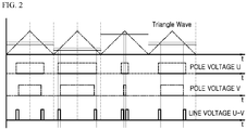
- FIGS. 2 and 3 are diagrams for illustrating a method for generating a random PWM voltage reference signal according to an exemplary embodiment of the present disclosure.
- the present disclosure relates to a method for achieving random PWM by RPPWM scheme, in which switching frequency is randomly changed, unlike existing methods. That is, RPPWM scheme uses a fixed switching frequency and thus does not require a process of synchronizing a triangle wave operation and the operations required by RFPWM scheme shown in FIG. 1 .
- the present disclosure provides a novel RPPWM technique by simply adding a randomly-generated compensation value to an existing MinMaxPWM algorithm.
- FIG. 2 shows a triangle wave generated with a constant frequency along time (t) axis, reference voltages of U-phase and V-phase of a three-phase voltage, and a line voltage (U-V) corresponding to the difference therebetween.
- the reference voltage is a voltage signal for controlling an output voltage from an inverter by using a feedback value such as velocity information or current information of a motor.
- the PI controller 40 may output a reference voltage by using the velocity information W* of the motor.
- the line voltage i.e., the difference between the U-phase voltage and the V-phase voltage is maintained constant throughout the periods of the triangle wave
- the offset value OFFSET varies randomly, which is to be added to the U and V values. Accordingly, it can be seen from FIG. 2 that the positions of pulses of the line voltage vary among different periods. In other words, the line voltage pulses concentrate on the center of a PWM period when the offset value becomes large, while the line voltage pulses are located at edges of a PWM period when the offset value becomes small.
- the positions of the line voltage pulses change in each of the triangle wave.
- the same effect can be achieved as when the switching frequency is changed. That is, by generating random variables and using them as the offset values, the positions of the line voltage pulses can be randomly changed among different periods of the triangle wave.
- the output value i.e., the sum of the applied reference value and the offset value may exceed the maximum limit value of the reference value (the peak of the triangle wave).
- the maximum limit value of the reference value the peak of the triangle wave.
- the offset values so that the sum is located in the range between the maximum limit and the minimum limit of the reference value. That is, the maximum limit and minimum limit of the reference value are fixed, while the reference value itself may vary among different periods. Therefore, in order to maintain the output value in an appropriate range, the random variables to be used as the offset values have to be changed accordingly by scaling.
- the distance between the maximum reference value and the peak of the triangle wave (maximum limit value), and the distance between the minimum reference value and the trough of the triangle wave (minimum limit value) vary among different periods. Accordingly, in order to calculate the range within which the positions of the pulses may change, the two distances have to be calculated at every period.
- the average of the maximum reference value and the minimum reference value (V bs *+V cs *)/2 is located in the center of the triangle wave (see FIG. 3(b) ). If the absolute values of the maximum reference value V* max and the minimum reference value V* min of the three phase voltage references are equal to each other, the active voltage vector depending on the switching state as a result of comparison with the triangle wave is located in the very center of the period of voltage modulation.
- An arbitrary value V sn may be determined so that the absolute value of the maximum reference value V* max becomes equal to that of the minimum reference value V* min when the arbitrary value V sn is added thereto. It can be seen from Equation 1 that the arbitrary value Vsn thus determined is the average (V* max + V* min )/2 of the maximum reference value and the minimum reference value.
- the distance between the maximum reference value and the maximum value of the triangle wave corresponding to the maximum limit of the reference value becomes equal to the distance between the minimum reference value and the minimum value of the triangle wave corresponding to the minimum limit value of the reference value. Accordingly, the variation range between the maximum reference value and the maximum value of the triangle wave or between the minimum reference value and the minimum value of the triangle wave is calculated to determine an offset value, and "+/-" conversion is performed on it, such that output values randomly generated within a range that does not exceed the maximum limit value and the minimum limit value of the reference value.
- V as *, V bs *, V cs * denotes the reference values calculated from the applied three-phase voltage reference
- V as **, V bs **, V cs ** denotes adjusted reference values obtained by performing the MinMaxPWM operation on the three phase reference values, respectively.
- V as ***, V bs ***, V cs *** denotes output values obtained by applying the offset value to the adjusted reference values.
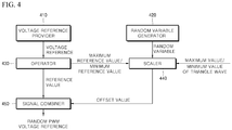
- FIG. 4 is a block diagram for illustrating an apparatus for generating a random PWM voltage reference signal according to an exemplary embodiment of the present disclosure.
- the apparatus for generating a random PWM voltage reference signal includes a voltage reference provider 410, a random variable generator 420, an operator 430, a scaler 440, a signal combiner 450 and the like.
- the voltage reference provider 410 provides ordinary three-phase voltage references.
- the random variable generator 420 generates random variables applied as offset values at every period of a voltage reference.
- the random variable generator 420 may generate random variables at every natural number multiple of the period of a voltage reference. In this case, random variables generated in a period corresponding to the period of the voltage reference may be selectively used.
- any of well-known random variable generating techniques such as mid-square method and linear congruential method may be applied to the random variable generator 420.
- the operator 430 performs MinMaxPWM operation by using a current voltage reference sent from the voltage reference provider 410.
- the scaler 440 scales the random variables with a range set from the maximum value or the minimum value of the adjusted reference values calculated via MinMaxPWM operation and the maximum value or the minimum value of the triangle wave, thereby generating an offset value.
- the random variables are generated as numbers within a predetermined range (e.g., 1 to 100) and the ranges set by the maximum value of adjusted reference values and the maximum value of a triangle wave during three periods of the triangle wave are 8, 10 and 15, respectively. If the random variable in the first period of the triangle wave is 80, a scaling ratio of 8 * (80 / 100) may be applied. Accordingly, the offset value is approximately 6.
- the offset value is 5. If the random variable in the third period of the triangle wave is 25, the offset value is approximately 4.
- the random variables generated by the random variable generator 420 may be created as offset values falling within in the ranges set by the scaler 440. Then, the offset values and the adjusted reference values may be combined by the signal combiner 450, such that a random PWM voltage reference can be generated.
- the operator 430 performs MinMaxPWM operation on the voltage references provided from the voltage reference provider 410 to obtain the adjusted reference values, and the adjusted reference values are delivered to the scaler 44 and the signal combiner 450. Then, the adjusted reference values delivered to the scaler 440 are used to scale the random variables generated by the random variable generator 420. Then, the offset values generated by scaling the random variables are combined with the adjusted reference values by the signal combiner450, such that the random PWM voltage reference signal varying among different periods can be generated.
- the maximum reference value and the minimum reference value can be equally distant from the center of the triangle wave.
- the active vector may be applied in a section between the maximum reference value and the maximum value of the triangle wave and between the minimum reference value and the minimum value of the triangle wave.
- the scaler 440 performs scaling so that the random variables generated by the random variable generator 420 are located in the section, and accordingly the offset values are created from the scaling and are applied to the adjusted reference values provided from the operator 430, thereby creating the random PWM reference signal.
- the maximum value of the triangle wave may be used.
- the minimum reference value the minimum value of the triangle wave may preferably be used.
- MinMaxPWM operation may be carried out according to Equation 1.
- FIG. 5 is a flowchart for illustrating a method for generating a random PWM voltage reference signal according to an exemplary embodiment of the present disclosure.
- the method for generating a random PWM voltage reference signal includes providing reference values S510, generating random variables S520, scaling S530, and combining signals S540 and the like.
- the providing S510 provides three phase voltage references having a constant frequency.
- the generating S520 generates random variables for each of the periods of the voltage references.
- the scaling S530 includes calculating adjusted reference values by performing MinMaxPWM operation on the voltage references sent from the providing S510 (step S532).
- the scaling S530 includes generating offset values by scaling the random variables within a range formed by the difference between the maximum reference value or the minimum reference value of the adjusted reference value and the maximum value or The minimum value of the triangle wave (step S534).
- offset values can be generated so that the output value as combination of the reference values and the offset values is located within a range between the maximum value and the minimum value of the triangle wave that are the maximum limit and the minimum limit of the reference values.
- the offset values thus generated are combined with the adjusted reference values via the combining S540, such that a real-time random PWM voltage reference signal can be generated.
- exemplary embodiments of the present disclosure relate to a method for implementing a random PWM that does not require synchronization process among triangle wave operation or operations.
- a random PWM region signal can be generated efficiently, which is already described above.
- a random PWM voltage reference signal can be generated more simply by using MinMaxPWM operation that is a modulation scheme maximizing the voltage utilization, such that it can be widely applied to general inverters and reduce electromagnetic noise of inverters effectively.
Landscapes
- Engineering & Computer Science (AREA)
- Power Engineering (AREA)
- Physics & Mathematics (AREA)
- Electromagnetism (AREA)
- Inverter Devices (AREA)
Applications Claiming Priority (1)
| Application Number | Priority Date | Filing Date | Title |
|---|---|---|---|
| KR1020160019374A KR101779698B1 (ko) | 2016-02-18 | 2016-02-18 | Pwm 신호의 생성 방법 및 장치 |
Publications (2)
| Publication Number | Publication Date |
|---|---|
| EP3208932A1 true EP3208932A1 (de) | 2017-08-23 |
| EP3208932B1 EP3208932B1 (de) | 2019-09-04 |
Family
ID=57326165
Family Applications (1)
| Application Number | Title | Priority Date | Filing Date |
|---|---|---|---|
| EP16193040.9A Active EP3208932B1 (de) | 2016-02-18 | 2016-10-10 | Verfahren und vorrichtung zur erzeugung eines pwm-signals |
Country Status (6)
| Country | Link |
|---|---|
| US (1) | US10177754B2 (de) |
| EP (1) | EP3208932B1 (de) |
| JP (1) | JP6441879B2 (de) |
| KR (1) | KR101779698B1 (de) |
| CN (1) | CN107204718B (de) |
| ES (1) | ES2756530T3 (de) |
Cited By (1)
| Publication number | Priority date | Publication date | Assignee | Title |
|---|---|---|---|---|
| JP2023100015A (ja) * | 2022-01-05 | 2023-07-18 | ローム株式会社 | クロック信号生成回路、dc/dcコンバータ、pwm信号生成装置及び車両 |
Families Citing this family (6)
| Publication number | Priority date | Publication date | Assignee | Title |
|---|---|---|---|---|
| KR102589033B1 (ko) | 2018-07-17 | 2023-10-17 | 현대자동차주식회사 | 모터 구동을 위한 인버터 제어 장치 및 방법 |
| KR102674664B1 (ko) | 2019-04-22 | 2024-06-11 | 현대자동차주식회사 | 저전압 직류 변환장치의 전압지령의 분해능을 상향시키는 시스템 및 방법 |
| JP7402009B2 (ja) * | 2019-10-10 | 2023-12-20 | 三星電子株式会社 | Pwm制御インバータ |
| KR102844828B1 (ko) * | 2019-11-20 | 2025-08-11 | 에스케이온 주식회사 | Pwm 신호를 이용한 부하 제어 장치 및 방법 |
| CN111342421B (zh) * | 2020-03-27 | 2025-04-11 | 珠海格力电器股份有限公司 | 一种硬件保护电路、方法及用电系统 |
| US12474682B2 (en) * | 2022-11-16 | 2025-11-18 | Infineon Technologies Ag | Switching frequency variation for a motor |
Citations (2)
| Publication number | Priority date | Publication date | Assignee | Title |
|---|---|---|---|---|
| US5706186A (en) * | 1996-09-23 | 1998-01-06 | Allen-Bradley Company, Inc. | Hybrid pulse width modulation method and apparatus |
| KR20010073638A (ko) | 2000-01-19 | 2001-08-01 | 구자홍 | 랜덤 pwm을 이용한 압축기의 소음 저감장치 및 그의제어방법 |
Family Cites Families (10)
| Publication number | Priority date | Publication date | Assignee | Title |
|---|---|---|---|---|
| US5258904A (en) * | 1992-04-23 | 1993-11-02 | Ford Motor Company | Dither control method of PWM inverter to improve low level motor torque control |
| JP3841282B2 (ja) | 2002-03-20 | 2006-11-01 | 株式会社安川電機 | Pwmインバータ装置 |
| US7130346B2 (en) | 2004-05-14 | 2006-10-31 | Freescale Semiconductor, Inc. | Method and apparatus having a digital PWM signal generator with integral noise shaping |
| KR101593438B1 (ko) | 2009-09-16 | 2016-02-12 | 삼성전자주식회사 | 하프-브리지 3-레벨 펄스폭 변조 증폭기, 이의 구동 방법 및 오디오 처리 장치 |
| US8421397B2 (en) | 2011-04-11 | 2013-04-16 | Eaton Corporation | System and method for fast start-up of an induction motor |
| KR101284923B1 (ko) * | 2012-02-24 | 2013-07-10 | 중앙대학교 산학협력단 | 인버터 소음 저감을 위한 랜덤 pwm 발생장치 |
| US8649887B2 (en) * | 2012-05-22 | 2014-02-11 | GM Global Technology Operations LLC | Methods, systems and apparatus for implementing dithering in motor drive system for controlling operation of an electric machine |
| KR20140013863A (ko) | 2012-07-28 | 2014-02-05 | 김래영 | 3-레벨 중성점 클램핑 다이오드 인버터 회로 및 이의 펄스폭 제어 방법 |
| US9270168B2 (en) * | 2013-03-15 | 2016-02-23 | Hamilton Sundstrand Corporation | Electromagnetic interference (EMI) reduction in multi-level power converter |
| KR101508834B1 (ko) | 2013-07-02 | 2015-04-06 | 엘에스산전 주식회사 | 인버터에서 출력전류 검출을 위한 전압지령 수정장치 |
-
2016
- 2016-02-18 KR KR1020160019374A patent/KR101779698B1/ko active Active
- 2016-10-10 EP EP16193040.9A patent/EP3208932B1/de active Active
- 2016-10-10 ES ES16193040T patent/ES2756530T3/es active Active
- 2016-11-01 CN CN201610937533.1A patent/CN107204718B/zh active Active
- 2016-11-07 JP JP2016217606A patent/JP6441879B2/ja not_active Expired - Fee Related
- 2016-11-21 US US15/357,541 patent/US10177754B2/en active Active
Patent Citations (2)
| Publication number | Priority date | Publication date | Assignee | Title |
|---|---|---|---|---|
| US5706186A (en) * | 1996-09-23 | 1998-01-06 | Allen-Bradley Company, Inc. | Hybrid pulse width modulation method and apparatus |
| KR20010073638A (ko) | 2000-01-19 | 2001-08-01 | 구자홍 | 랜덤 pwm을 이용한 압축기의 소음 저감장치 및 그의제어방법 |
Non-Patent Citations (2)
| Title |
|---|
| DAE-WOONG JUNG: "Unified analysis of PWM method for three phase voltage source inverter using offset voltage", PH.D. DISSERTATION, February 2000 (2000-02-01) |
| HEE-JUNG KIM ET AL: "A new discontinuous PWM strategy of neutral-point clamped inverter", 2013 IEEE INDUSTRY APPLICATIONS SOCIETY ANNUAL MEETING, vol. 3, 2 January 2000 (2000-01-02), pages 2017, XP055363744, ISSN: 0197-2618, DOI: 10.1109/IAS.2000.882154 * |
Cited By (2)
| Publication number | Priority date | Publication date | Assignee | Title |
|---|---|---|---|---|
| JP2023100015A (ja) * | 2022-01-05 | 2023-07-18 | ローム株式会社 | クロック信号生成回路、dc/dcコンバータ、pwm信号生成装置及び車両 |
| JP7762574B2 (ja) | 2022-01-05 | 2025-10-30 | ローム株式会社 | クロック信号生成回路、dc/dcコンバータ、pwm信号生成装置及び車両 |
Also Published As
| Publication number | Publication date |
|---|---|
| KR101779698B1 (ko) | 2017-09-18 |
| US10177754B2 (en) | 2019-01-08 |
| JP6441879B2 (ja) | 2018-12-19 |
| EP3208932B1 (de) | 2019-09-04 |
| KR20170097511A (ko) | 2017-08-28 |
| ES2756530T3 (es) | 2020-04-27 |
| CN107204718B (zh) | 2020-02-21 |
| US20170244399A1 (en) | 2017-08-24 |
| JP2017147925A (ja) | 2017-08-24 |
| CN107204718A (zh) | 2017-09-26 |
Similar Documents
| Publication | Publication Date | Title |
|---|---|---|
| EP3208932B1 (de) | Verfahren und vorrichtung zur erzeugung eines pwm-signals | |
| US9998059B2 (en) | Motor driving apparatus | |
| US7084603B2 (en) | Motor control device | |
| US20140176027A1 (en) | Control system for three-phase rotary machine | |
| US10696141B2 (en) | Synchronous motor control device and method of controlling synchronous motor | |
| KR20160122923A (ko) | 3상 인버터의 옵셋 전압 생성 장치 및 방법 | |
| US9543868B2 (en) | Apparatus for controlling rotary electric machine | |
| JP2011147287A (ja) | 電動機の磁極位置推定装置 | |
| CN110729944B (zh) | 用于驱动电机的逆变器控制装置和方法 | |
| KR102712337B1 (ko) | 모터 구동을 위한 인버터 제어 장치 및 방법 | |
| US9755563B2 (en) | Inverter control apparatus and inverter apparatus | |
| JP5752214B2 (ja) | 同期機制御装置 | |
| US6232730B1 (en) | Brushless motor driving circuit and a method of controlling the brushless motor driving circuit | |
| EP2802072A1 (de) | Stromwandler | |
| KR20190100801A (ko) | 모터 구동을 위한 인버터 제어 시스템 및 방법 | |
| EP2618480A2 (de) | Motorsteuerungsvorrichtung und Klimaanlage | |
| JP7094859B2 (ja) | モータ制御装置及びモータ制御方法 | |
| US20120242262A1 (en) | Control apparatus for electric motor | |
| US9806652B2 (en) | System of controlling induction electric motor | |
| CN110800206A (zh) | 电机控制装置和电机控制方法 | |
| CN110785923A (zh) | 电机控制装置和电机控制方法 | |
| JP2020156157A (ja) | インバータ装置 | |
| JP2016036195A (ja) | モータ制御装置及び冷蔵庫 | |
| JP2006081322A (ja) | 交流電動機の制御装置 | |
| JP2003033043A (ja) | インバータ装置 |
Legal Events
| Date | Code | Title | Description |
|---|---|---|---|
| PUAI | Public reference made under article 153(3) epc to a published international application that has entered the european phase |
Free format text: ORIGINAL CODE: 0009012 |
|
| STAA | Information on the status of an ep patent application or granted ep patent |
Free format text: STATUS: THE APPLICATION HAS BEEN PUBLISHED |
|
| AK | Designated contracting states |
Kind code of ref document: A1 Designated state(s): AL AT BE BG CH CY CZ DE DK EE ES FI FR GB GR HR HU IE IS IT LI LT LU LV MC MK MT NL NO PL PT RO RS SE SI SK SM TR |
|
| AX | Request for extension of the european patent |
Extension state: BA ME |
|
| STAA | Information on the status of an ep patent application or granted ep patent |
Free format text: STATUS: REQUEST FOR EXAMINATION WAS MADE |
|
| STAA | Information on the status of an ep patent application or granted ep patent |
Free format text: STATUS: EXAMINATION IS IN PROGRESS |
|
| 17P | Request for examination filed |
Effective date: 20180222 |
|
| RBV | Designated contracting states (corrected) |
Designated state(s): AL AT BE BG CH CY CZ DE DK EE ES FI FR GB GR HR HU IE IS IT LI LT LU LV MC MK MT NL NO PL PT RO RS SE SI SK SM TR |
|
| 17Q | First examination report despatched |
Effective date: 20180321 |
|
| GRAP | Despatch of communication of intention to grant a patent |
Free format text: ORIGINAL CODE: EPIDOSNIGR1 |
|
| STAA | Information on the status of an ep patent application or granted ep patent |
Free format text: STATUS: GRANT OF PATENT IS INTENDED |
|
| INTG | Intention to grant announced |
Effective date: 20190402 |
|
| GRAS | Grant fee paid |
Free format text: ORIGINAL CODE: EPIDOSNIGR3 |
|
| GRAA | (expected) grant |
Free format text: ORIGINAL CODE: 0009210 |
|
| STAA | Information on the status of an ep patent application or granted ep patent |
Free format text: STATUS: THE PATENT HAS BEEN GRANTED |
|
| AK | Designated contracting states |
Kind code of ref document: B1 Designated state(s): AL AT BE BG CH CY CZ DE DK EE ES FI FR GB GR HR HU IE IS IT LI LT LU LV MC MK MT NL NO PL PT RO RS SE SI SK SM TR |
|
| REG | Reference to a national code |
Ref country code: GB Ref legal event code: FG4D |
|
| REG | Reference to a national code |
Ref country code: CH Ref legal event code: EP |
|
| REG | Reference to a national code |
Ref country code: AT Ref legal event code: REF Ref document number: 1176779 Country of ref document: AT Kind code of ref document: T Effective date: 20190915 |
|
| REG | Reference to a national code |
Ref country code: DE Ref legal event code: R096 Ref document number: 602016019793 Country of ref document: DE |
|
| REG | Reference to a national code |
Ref country code: IE Ref legal event code: FG4D |
|
| REG | Reference to a national code |
Ref country code: NL Ref legal event code: MP Effective date: 20190904 |
|
| REG | Reference to a national code |
Ref country code: LT Ref legal event code: MG4D |
|
| PG25 | Lapsed in a contracting state [announced via postgrant information from national office to epo] |
Ref country code: NO Free format text: LAPSE BECAUSE OF FAILURE TO SUBMIT A TRANSLATION OF THE DESCRIPTION OR TO PAY THE FEE WITHIN THE PRESCRIBED TIME-LIMIT Effective date: 20191204 Ref country code: BG Free format text: LAPSE BECAUSE OF FAILURE TO SUBMIT A TRANSLATION OF THE DESCRIPTION OR TO PAY THE FEE WITHIN THE PRESCRIBED TIME-LIMIT Effective date: 20191204 Ref country code: SE Free format text: LAPSE BECAUSE OF FAILURE TO SUBMIT A TRANSLATION OF THE DESCRIPTION OR TO PAY THE FEE WITHIN THE PRESCRIBED TIME-LIMIT Effective date: 20190904 Ref country code: FI Free format text: LAPSE BECAUSE OF FAILURE TO SUBMIT A TRANSLATION OF THE DESCRIPTION OR TO PAY THE FEE WITHIN THE PRESCRIBED TIME-LIMIT Effective date: 20190904 Ref country code: LT Free format text: LAPSE BECAUSE OF FAILURE TO SUBMIT A TRANSLATION OF THE DESCRIPTION OR TO PAY THE FEE WITHIN THE PRESCRIBED TIME-LIMIT Effective date: 20190904 Ref country code: HR Free format text: LAPSE BECAUSE OF FAILURE TO SUBMIT A TRANSLATION OF THE DESCRIPTION OR TO PAY THE FEE WITHIN THE PRESCRIBED TIME-LIMIT Effective date: 20190904 |
|
| PG25 | Lapsed in a contracting state [announced via postgrant information from national office to epo] |
Ref country code: GR Free format text: LAPSE BECAUSE OF FAILURE TO SUBMIT A TRANSLATION OF THE DESCRIPTION OR TO PAY THE FEE WITHIN THE PRESCRIBED TIME-LIMIT Effective date: 20191205 Ref country code: RS Free format text: LAPSE BECAUSE OF FAILURE TO SUBMIT A TRANSLATION OF THE DESCRIPTION OR TO PAY THE FEE WITHIN THE PRESCRIBED TIME-LIMIT Effective date: 20190904 Ref country code: LV Free format text: LAPSE BECAUSE OF FAILURE TO SUBMIT A TRANSLATION OF THE DESCRIPTION OR TO PAY THE FEE WITHIN THE PRESCRIBED TIME-LIMIT Effective date: 20190904 Ref country code: AL Free format text: LAPSE BECAUSE OF FAILURE TO SUBMIT A TRANSLATION OF THE DESCRIPTION OR TO PAY THE FEE WITHIN THE PRESCRIBED TIME-LIMIT Effective date: 20190904 |
|
| REG | Reference to a national code |
Ref country code: AT Ref legal event code: MK05 Ref document number: 1176779 Country of ref document: AT Kind code of ref document: T Effective date: 20190904 |
|
| REG | Reference to a national code |
Ref country code: ES Ref legal event code: FG2A Ref document number: 2756530 Country of ref document: ES Kind code of ref document: T3 Effective date: 20200427 |
|
| PG25 | Lapsed in a contracting state [announced via postgrant information from national office to epo] |
Ref country code: PT Free format text: LAPSE BECAUSE OF FAILURE TO SUBMIT A TRANSLATION OF THE DESCRIPTION OR TO PAY THE FEE WITHIN THE PRESCRIBED TIME-LIMIT Effective date: 20200106 Ref country code: PL Free format text: LAPSE BECAUSE OF FAILURE TO SUBMIT A TRANSLATION OF THE DESCRIPTION OR TO PAY THE FEE WITHIN THE PRESCRIBED TIME-LIMIT Effective date: 20190904 Ref country code: NL Free format text: LAPSE BECAUSE OF FAILURE TO SUBMIT A TRANSLATION OF THE DESCRIPTION OR TO PAY THE FEE WITHIN THE PRESCRIBED TIME-LIMIT Effective date: 20190904 Ref country code: AT Free format text: LAPSE BECAUSE OF FAILURE TO SUBMIT A TRANSLATION OF THE DESCRIPTION OR TO PAY THE FEE WITHIN THE PRESCRIBED TIME-LIMIT Effective date: 20190904 Ref country code: RO Free format text: LAPSE BECAUSE OF FAILURE TO SUBMIT A TRANSLATION OF THE DESCRIPTION OR TO PAY THE FEE WITHIN THE PRESCRIBED TIME-LIMIT Effective date: 20190904 Ref country code: EE Free format text: LAPSE BECAUSE OF FAILURE TO SUBMIT A TRANSLATION OF THE DESCRIPTION OR TO PAY THE FEE WITHIN THE PRESCRIBED TIME-LIMIT Effective date: 20190904 |
|
| PG25 | Lapsed in a contracting state [announced via postgrant information from national office to epo] |
Ref country code: IS Free format text: LAPSE BECAUSE OF FAILURE TO SUBMIT A TRANSLATION OF THE DESCRIPTION OR TO PAY THE FEE WITHIN THE PRESCRIBED TIME-LIMIT Effective date: 20200224 Ref country code: CZ Free format text: LAPSE BECAUSE OF FAILURE TO SUBMIT A TRANSLATION OF THE DESCRIPTION OR TO PAY THE FEE WITHIN THE PRESCRIBED TIME-LIMIT Effective date: 20190904 Ref country code: SK Free format text: LAPSE BECAUSE OF FAILURE TO SUBMIT A TRANSLATION OF THE DESCRIPTION OR TO PAY THE FEE WITHIN THE PRESCRIBED TIME-LIMIT Effective date: 20190904 Ref country code: SM Free format text: LAPSE BECAUSE OF FAILURE TO SUBMIT A TRANSLATION OF THE DESCRIPTION OR TO PAY THE FEE WITHIN THE PRESCRIBED TIME-LIMIT Effective date: 20190904 |
|
| REG | Reference to a national code |
Ref country code: CH Ref legal event code: PL |
|
| REG | Reference to a national code |
Ref country code: DE Ref legal event code: R097 Ref document number: 602016019793 Country of ref document: DE |
|
| PLBE | No opposition filed within time limit |
Free format text: ORIGINAL CODE: 0009261 |
|
| STAA | Information on the status of an ep patent application or granted ep patent |
Free format text: STATUS: NO OPPOSITION FILED WITHIN TIME LIMIT |
|
| PG2D | Information on lapse in contracting state deleted |
Ref country code: IS |
|
| PG25 | Lapsed in a contracting state [announced via postgrant information from national office to epo] |
Ref country code: DK Free format text: LAPSE BECAUSE OF FAILURE TO SUBMIT A TRANSLATION OF THE DESCRIPTION OR TO PAY THE FEE WITHIN THE PRESCRIBED TIME-LIMIT Effective date: 20190904 Ref country code: LI Free format text: LAPSE BECAUSE OF NON-PAYMENT OF DUE FEES Effective date: 20191031 Ref country code: LU Free format text: LAPSE BECAUSE OF NON-PAYMENT OF DUE FEES Effective date: 20191010 Ref country code: CH Free format text: LAPSE BECAUSE OF NON-PAYMENT OF DUE FEES Effective date: 20191031 Ref country code: IS Free format text: LAPSE BECAUSE OF FAILURE TO SUBMIT A TRANSLATION OF THE DESCRIPTION OR TO PAY THE FEE WITHIN THE PRESCRIBED TIME-LIMIT Effective date: 20200105 |
|
| 26N | No opposition filed |
Effective date: 20200605 |
|
| REG | Reference to a national code |
Ref country code: BE Ref legal event code: MM Effective date: 20191031 |
|
| PG25 | Lapsed in a contracting state [announced via postgrant information from national office to epo] |
Ref country code: BE Free format text: LAPSE BECAUSE OF NON-PAYMENT OF DUE FEES Effective date: 20191031 Ref country code: MC Free format text: LAPSE BECAUSE OF FAILURE TO SUBMIT A TRANSLATION OF THE DESCRIPTION OR TO PAY THE FEE WITHIN THE PRESCRIBED TIME-LIMIT Effective date: 20190904 Ref country code: SI Free format text: LAPSE BECAUSE OF FAILURE TO SUBMIT A TRANSLATION OF THE DESCRIPTION OR TO PAY THE FEE WITHIN THE PRESCRIBED TIME-LIMIT Effective date: 20190904 |
|
| PG25 | Lapsed in a contracting state [announced via postgrant information from national office to epo] |
Ref country code: IE Free format text: LAPSE BECAUSE OF NON-PAYMENT OF DUE FEES Effective date: 20191010 |
|
| PG25 | Lapsed in a contracting state [announced via postgrant information from national office to epo] |
Ref country code: CY Free format text: LAPSE BECAUSE OF FAILURE TO SUBMIT A TRANSLATION OF THE DESCRIPTION OR TO PAY THE FEE WITHIN THE PRESCRIBED TIME-LIMIT Effective date: 20190904 |
|
| PG25 | Lapsed in a contracting state [announced via postgrant information from national office to epo] |
Ref country code: MT Free format text: LAPSE BECAUSE OF FAILURE TO SUBMIT A TRANSLATION OF THE DESCRIPTION OR TO PAY THE FEE WITHIN THE PRESCRIBED TIME-LIMIT Effective date: 20190904 Ref country code: HU Free format text: LAPSE BECAUSE OF FAILURE TO SUBMIT A TRANSLATION OF THE DESCRIPTION OR TO PAY THE FEE WITHIN THE PRESCRIBED TIME-LIMIT; INVALID AB INITIO Effective date: 20161010 |
|
| PG25 | Lapsed in a contracting state [announced via postgrant information from national office to epo] |
Ref country code: TR Free format text: LAPSE BECAUSE OF FAILURE TO SUBMIT A TRANSLATION OF THE DESCRIPTION OR TO PAY THE FEE WITHIN THE PRESCRIBED TIME-LIMIT Effective date: 20190904 |
|
| PG25 | Lapsed in a contracting state [announced via postgrant information from national office to epo] |
Ref country code: MK Free format text: LAPSE BECAUSE OF FAILURE TO SUBMIT A TRANSLATION OF THE DESCRIPTION OR TO PAY THE FEE WITHIN THE PRESCRIBED TIME-LIMIT Effective date: 20190904 |
|
| PGFP | Annual fee paid to national office [announced via postgrant information from national office to epo] |
Ref country code: GB Payment date: 20220905 Year of fee payment: 7 |
|
| PGFP | Annual fee paid to national office [announced via postgrant information from national office to epo] |
Ref country code: ES Payment date: 20221114 Year of fee payment: 7 |
|
| P01 | Opt-out of the competence of the unified patent court (upc) registered |
Effective date: 20230625 |
|
| GBPC | Gb: european patent ceased through non-payment of renewal fee |
Effective date: 20231010 |
|
| PG25 | Lapsed in a contracting state [announced via postgrant information from national office to epo] |
Ref country code: GB Free format text: LAPSE BECAUSE OF NON-PAYMENT OF DUE FEES Effective date: 20231010 |
|
| PG25 | Lapsed in a contracting state [announced via postgrant information from national office to epo] |
Ref country code: GB Free format text: LAPSE BECAUSE OF NON-PAYMENT OF DUE FEES Effective date: 20231010 |
|
| REG | Reference to a national code |
Ref country code: ES Ref legal event code: FD2A Effective date: 20241127 |
|
| PG25 | Lapsed in a contracting state [announced via postgrant information from national office to epo] |
Ref country code: ES Free format text: LAPSE BECAUSE OF NON-PAYMENT OF DUE FEES Effective date: 20231011 |
|
| PG25 | Lapsed in a contracting state [announced via postgrant information from national office to epo] |
Ref country code: ES Free format text: LAPSE BECAUSE OF NON-PAYMENT OF DUE FEES Effective date: 20231011 |
|
| PGFP | Annual fee paid to national office [announced via postgrant information from national office to epo] |
Ref country code: IT Payment date: 20250909 Year of fee payment: 10 |
|
| PGFP | Annual fee paid to national office [announced via postgrant information from national office to epo] |
Ref country code: FR Payment date: 20250909 Year of fee payment: 10 |
|
| PGFP | Annual fee paid to national office [announced via postgrant information from national office to epo] |
Ref country code: DE Payment date: 20250908 Year of fee payment: 10 |