EP3201832B1 - Fingerabdruck- oder handflächensensor - Google Patents
Fingerabdruck- oder handflächensensor Download PDFInfo
- Publication number
- EP3201832B1 EP3201832B1 EP15788117.8A EP15788117A EP3201832B1 EP 3201832 B1 EP3201832 B1 EP 3201832B1 EP 15788117 A EP15788117 A EP 15788117A EP 3201832 B1 EP3201832 B1 EP 3201832B1
- Authority
- EP
- European Patent Office
- Prior art keywords
- sensor
- cell
- node
- cells
- acquisition
- Prior art date
- Legal status (The legal status is an assumption and is not a legal conclusion. Google has not performed a legal analysis and makes no representation as to the accuracy of the status listed.)
- Active
Links
Images

Classifications
-
- G—PHYSICS
- G06—COMPUTING; CALCULATING OR COUNTING
- G06V—IMAGE OR VIDEO RECOGNITION OR UNDERSTANDING
- G06V40/00—Recognition of biometric, human-related or animal-related patterns in image or video data
- G06V40/10—Human or animal bodies, e.g. vehicle occupants or pedestrians; Body parts, e.g. hands
- G06V40/12—Fingerprints or palmprints
- G06V40/13—Sensors therefor
- G06V40/1306—Sensors therefor non-optical, e.g. ultrasonic or capacitive sensing
-
- A—HUMAN NECESSITIES
- A61—MEDICAL OR VETERINARY SCIENCE; HYGIENE
- A61B—DIAGNOSIS; SURGERY; IDENTIFICATION
- A61B5/00—Measuring for diagnostic purposes; Identification of persons
- A61B5/117—Identification of persons
- A61B5/1171—Identification of persons based on the shapes or appearances of their bodies or parts thereof
- A61B5/1172—Identification of persons based on the shapes or appearances of their bodies or parts thereof using fingerprinting
-
- G—PHYSICS
- G06—COMPUTING; CALCULATING OR COUNTING
- G06V—IMAGE OR VIDEO RECOGNITION OR UNDERSTANDING
- G06V40/00—Recognition of biometric, human-related or animal-related patterns in image or video data
- G06V40/10—Human or animal bodies, e.g. vehicle occupants or pedestrians; Body parts, e.g. hands
- G06V40/12—Fingerprints or palmprints
- G06V40/13—Sensors therefor
- G06V40/1318—Sensors therefor using electro-optical elements or layers, e.g. electroluminescent sensing
-
- G—PHYSICS
- G06—COMPUTING; CALCULATING OR COUNTING
- G06V—IMAGE OR VIDEO RECOGNITION OR UNDERSTANDING
- G06V40/00—Recognition of biometric, human-related or animal-related patterns in image or video data
- G06V40/10—Human or animal bodies, e.g. vehicle occupants or pedestrians; Body parts, e.g. hands
- G06V40/12—Fingerprints or palmprints
- G06V40/13—Sensors therefor
- G06V40/1329—Protecting the fingerprint sensor against damage caused by the finger
-
- G—PHYSICS
- G06—COMPUTING; CALCULATING OR COUNTING
- G06V—IMAGE OR VIDEO RECOGNITION OR UNDERSTANDING
- G06V40/00—Recognition of biometric, human-related or animal-related patterns in image or video data
- G06V40/10—Human or animal bodies, e.g. vehicle occupants or pedestrians; Body parts, e.g. hands
- G06V40/12—Fingerprints or palmprints
- G06V40/1365—Matching; Classification
-
- G—PHYSICS
- G06—COMPUTING; CALCULATING OR COUNTING
- G06V—IMAGE OR VIDEO RECOGNITION OR UNDERSTANDING
- G06V40/00—Recognition of biometric, human-related or animal-related patterns in image or video data
- G06V40/10—Human or animal bodies, e.g. vehicle occupants or pedestrians; Body parts, e.g. hands
- G06V40/12—Fingerprints or palmprints
- G06V40/1382—Detecting the live character of the finger, i.e. distinguishing from a fake or cadaver finger
- G06V40/1394—Detecting the live character of the finger, i.e. distinguishing from a fake or cadaver finger using acquisition arrangements
-
- H—ELECTRICITY
- H03—ELECTRONIC CIRCUITRY
- H03K—PULSE TECHNIQUE
- H03K17/00—Electronic switching or gating, i.e. not by contact-making and –breaking
- H03K17/94—Electronic switching or gating, i.e. not by contact-making and –breaking characterised by the way in which the control signals are generated
- H03K17/96—Touch switches
- H03K17/962—Capacitive touch switches
-
- H—ELECTRICITY
- H04—ELECTRIC COMMUNICATION TECHNIQUE
- H04N—PICTORIAL COMMUNICATION, e.g. TELEVISION
- H04N25/00—Circuitry of solid-state image sensors [SSIS]; Control thereof
- H04N25/70—SSIS architectures; Circuits associated therewith
- H04N25/76—Addressed sensors, e.g. MOS or CMOS sensors
- H04N25/77—Pixel circuitry, e.g. memories, A/D converters, pixel amplifiers, shared circuits or shared components
Definitions
- the present application relates to the field of fingerprint or palmar sensors.
- sensors have been proposed to perform an electronic acquisition of a fingerprint and / or palmar, that is to say to provide an image of the pattern formed by the ridges and hollows of the skin of a finger, several fingers, and / or the palm of the hand.
- optical sensors, capacitive sensors, thermal sensors, ultrasonic sensors, and electric field sensors have been proposed.
- Such sensors are disclosed in the documents WO2014 / 091093 or JP2006343229 .
- TFT Thin Film Transistor
- a support substrate one or several elementary acquisition cells, each elementary cell (or pixel) comprising an acquisition element, for example photoelectric, pyroelectric or capacitive, and one or more TFT transistors for controlling this element.
- transistor TFT we mean here, transistors formed by successive deposits of conductive, insulating and semiconductive layers on the support substrate.
- the semiconductor channel-forming region of the transistor is produced by depositing a layer of a semiconductor material, for example hydrogenated amorphous silicon or polycrystalline silicon (polycrystalline rendering after annealing, for example).
- this deposit may be preceded by a deposit of a conductive layer for forming a gate electrode, source or drain of the transistor.
- IGZO of the "Indium Gallium Zinc Oxide” - indium gallium zinc oxide
- This deposit may be preceded by a deposit of a conductive layer for forming a gate electrode, source or drain of the transistor.
- the impression sensors made in TFT technology have the advantage of being relatively inexpensive, in particular by virtue of the use of a support substrate made of a low-cost material such as glass (instead of a substrate made of monocrystalline silicon generally used to make transistors), and to be easily integrated in many types of electronic devices, and in particular in devices already using TFT technology to perform other functions, for example to make screens of display.
- TFT technology is particularly advantageous in the field of fingerprint sensors in which the surface of the sensor is substantially identical to the surface of the impression to be acquired, that is to say in which no optical focusing system (or objective) is placed between the sensor and the object whose image is to be acquired. Indeed, because of their large sizes, the realization of such sensors in and on silicon substrates would be a cost far too high for most applications.
- One embodiment provides a fingerprint or palm sensor comprising: on a support substrate, a plurality of elementary acquisition cells, made of TFT technology, each cell comprising a photodetector and a pyroelectric conversion element connected to the same capacitive reading node of the cell, and a read circuit connecting the capacitive read node of the cell to a conductive output track of the cell a source bright lighting; and a heat source distinct from the light source.
- the support substrate is transparent.
- the photodetector and the pyroelectric conversion element are connected in parallel.
- the senor comprises a circuit adapted to control the acquisition of a thermal image and the acquisition of an optical image by the cells of the sensor, this circuit being adapted, during the entire acquisition phase of the optical image, to turn on the light source and keep the heat source off, and, during the entire acquisition phase of the thermal image, to keep the light source off.
- the senor comprises a circuit adapted to control the acquisition of a thermal image and the acquisition of an optical image by the cells of the sensor, this circuit being adapted to implement the acquisition of thermal image during part of an integration period of the acquisition phase of the optical image during which the light source is turned on.
- the photodetector and the pyroelectric conversion element are connected to a capacitive read node of the cell.
- each cell the photodetector and the pyroelectric conversion element are connected to an intermediate node of the cell, the intermediate node being connected to the capacitive reading node of the cell by a selection transistor, and each cell further comprising: a reference capacitor connected between the read capacitive node and an application node of a control signal; and an electrode connected to the capacitive readout node, the electrode being coated with a dielectric layer and being adapted to form a capacitance with the skin of a user for capacitive acquisition of a fingerprint image.
- the photodetector and the pyroelectric conversion element are connected to a same selection transistor allowing, in the open state, to isolate the photodetector from the pyroelectric element.
- the cells are arrayed in rows and columns, and the heat source is controllable to heat the cells line by line.
- the cells are voltage-read cells, each cell comprising: a reset transistor connecting the read capacitive node to an application node of a reset potential and a read circuit of each cell comprising a follower source-mounted transistor, whose gate is connected to the read node, and whose source is connected to an output track of the cell via a read transistor.
- the cells are load-reading cells, the read circuit of each cell comprising a read transistor connecting the read node to an output track of the cell.
- the figure 1 is an electrical diagram illustrating an example of an optical TFT fingerprint sensor 100.
- the sensor 100 comprises a plurality of identical or similar elementary acquisition cells 101 made in TFT technology on one side of a transparent support substrate, for example made of glass, which will be hereinafter conventionally referred to as the upper face of the substrate.
- a single cell 101 has been represented on the figure 1 .
- Each cell 101 comprises a photodetector PS, for example a photodiode whose anode is connected to an application node of a reference potential GND (for example ground), and whose cathode is connected to a capacitive read node. SN of the cell.
- GND for example ground
- the photodetector PS is a PIN type photodiode, or an organic photodiode.
- the capacity of the reading node SN has been represented in dashed lines in the form of a capacitor whose one electrode is connected to the node SN and whose other electrode is connected to the node GND.
- the capacity of the node SN may be a parasitic capacitance of another element of the cell, for example the parasitic capacitance of the photodiode PS (to which is added the parasitic capacitance of the transistor RS in the example represented), or a specific ability.
- the capacity of the SN node will not be represented in the following figures.
- Each cell 101 further comprises a read transistor RS connecting its read node SN to a conductive output track CL of the cell.
- the control gate of the transistor RS is connected to a VG RS node for applying a control potential of this transistor.
- the output track CL of the cell 101 is connected to an output stage 103 of the sensor.
- the output stage 103 comprises an operational amplifier 105 including an inverting input (-) connected to the track CL and a non-inverting input (+) connected to a node V pol of application of a potential of polarization.
- the output stage 103 further comprises an analog-to-digital converter 107 (ADC) whose input is connected to the output of the amplifier 105.
- the output stage further comprises a capacitor 109 in parallel with a control switch 111 between the inverting input (-) and the output of the amplifier 105.
- the sensor 100 further comprises a lighting light source, not shown.
- the light source is disposed on the side of the face of the substrate opposite to the cells 101, which will be hereinafter called conventionally the underside of the substrate.
- the operation of the sensor 100 is as follows.
- the user places one finger (or more) on or above the top surface of the sensor (cell side 101).
- the backlight light source disposed on the side of the substrate opposite the cells, illuminates the finger through transparent areas of the assembly formed by the support substrate and the cells 101.
- the light is then backscattered by the finger towards the photodiodes PS, with, at each cell 101, a more or less attenuation depending on whether the finger portion above the cell corresponds to a peak or a hollow of the skin of the finger.
- the light source can be placed above or next to the finger, the light then being transmitted by the finger towards the PS photodiodes of the sensor, with a greater or lesser attenuation depending on the portion of finger located above the cell corresponds to a ridge or hollow of the skin of the finger.
- the substrate may be non-transparent.
- the photogenerated charges are transferred to the output track CL of the cell (which may have been previously reset by closing the switch 111) via the transistor RS, and the signal resulting is read by the output stage 103 connected to the track CL.
- the RS transistor being bidirectional, it also resets the PS photodiode to a fixed potential before the start of a new integration period.
- the cells 101 may be connected to the same output track CL and share a same output stage 103 of the sensor.
- the cells 101 are for example arranged in a matrix according to rows and columns, the cells of one and the same column being connected to the same output track CL and to the same output stage 103, and the cells of distinct columns being connected to each other.
- the cells 101 are controllable simultaneously line by line, that is to say that the cells 101 of the same line have their nodes VG RS connected to the same control track and the cells 101 of lines distinct have their VG RS nodes connected to separate control tracks.
- the figure 2 is an electrical diagram illustrating an example of a thermal TFT fingerprint sensor 120.
- the sensor 120 of the figure 2 includes common elements with the sensor 100 of the figure 1 . These elements will not be described again.
- the sensor 120 differs from the sensor 100 mainly in that, in the sensor 120, elementary acquisition cells 121 of thermal type replace the elementary optical acquisition cells 101 of the sensor 100.
- the elementary cells 121 of the sensor of the figure 2 differ from the elementary cells 101 of the sensor of the figure 1 in that, in each cell 121, a pyroelectric conversion element PYR, connecting the reading node SN of the cell to the node GND, replaces the photodetector PS of the cells 101.
- the pyroelectric conversion element PYR typically comprises a layer of a pyroelectric material such as aluminum nitride (AlN), zinc oxide (ZnO), a polymer such as polyvinylidene fluoride (PVDF), whose pyroelectric coefficient is of the order of 40 ⁇ C / m 2 / K, a ceramic material of the PZT (lead titanozirconate) type, whose pyroelectric coefficient is of the order of 350 ⁇ C / m 2 / K, or a crystalline material of the TGS (Triglycine) type sulfate) or LiTaO 3 , arranged between two conductive layers respectively connected to the node SN and to the node GND.
- a pyroelectric material such as aluminum nitride (AlN), zinc oxide (ZnO), a polymer such as polyvinylidene fluoride (PVDF), whose pyroelectric coefficient is of the order of 40 ⁇ C
- the sensor 120 further differs from the sensor 100 of the figure 1 in that it does not include a backlight light source, but includes a heat source, not shown.
- the heat source may comprise a network of resistors regularly distributed over the surface of the sensor.
- the heat source comprises a resistance elementary cell, this resistance being disposed in the vicinity of the pyroelectric element of the cell.
- the resistors of the heat source are preferably arranged on the same side of the support substrate as the cells 101, that is to say on the side of the upper face of the substrate.
- the operation of the sensor 120 is as follows.
- the user has placed one finger (or more) on or above the top surface of the sensor (cell side 121).
- the heat source of the sensor is then turned on, and heats the pyroelectric conversion elements PYR which consequently generate electrical charges on the reading nodes SN of the corresponding cells 121.
- the amount of heat received by each pyroelectric conversion element PYR when the heat source is turned on is greater when the corresponding cell is surmounted by a hollow of the skin, than when it is surmounted by a ridge. Indeed, when the cell is surmounted by a ridge, the skin absorbs a larger part of the heat emitted by the source than when the cell is surmounted by a hollow.
- the amount of electric charges generated on its reading node SN is greater than when the cell is surmounted by a peak.
- the charges accumulated on the node SN are transferred to the output track CL of the cell via the transistor RS , and the resulting signal is read by the output stage 103 connected to the track CL. Since the RS transistor is bidirectional, it also resets the SN node before the start of a new integration period.
- the heat source is controlled to produce a heat pulse, and the cells are read a certain time after the start of the pulse, and / or shortly after the end of this pulse , so as to overcome the phenomena of thermalization causing, over time, the standardization of the accumulated charge levels on the reading nodes SN of the different cells.
- the cells 121 may be connected to the same output track CL and share a same output stage 103 of the sensor.
- the cells 121 are, for example, arranged in a matrix according to rows and columns, the cells of one and the same column being connected to the same output track CL and to the same output stage 103, and the cells of distinct columns being connected to separate output tracks CL and separate output stages 103.
- the cells 121 are controllable simultaneously line by line.
- the heat source is then controllable to heat cells 121 line by line. This makes it possible to scan the sensor line by line by synchronizing the ignition of the heat source with the reading of the cells, and thus to minimize the effects of the thermalization on the acquired image.
- the heat source may consist of conductive tracks extending along the lines of the sensor, for example metal tracks (for example in molybdenum or aluminum), tracks in a metal oxide, possibly transparent (eg indium tin oxide), polycrystalline silicon tracks, or conductive polymer tracks.
- metal tracks for example in molybdenum or aluminum
- tracks in a metal oxide possibly transparent (eg indium tin oxide), polycrystalline silicon tracks, or conductive polymer tracks.
- the elementary acquisition cells 101 and 121 are load-reading cells, that is to say that the reading of a cell passes through the transfer, on the output track CL of the cell (via the RS read transistor of the cell), accumulated charges on the read node SN of the cell.
- An advantage of the load-reading acquisition cells is that they are particularly simple and / or compact (a single transistor per cell in the examples of FIGS. Figures 1 and 2 ).
- Such cells are particularly suitable for TFT technologies, for example based on amorphous silicon or indium gallium zinc oxide, in which the transistors are relatively bulky.
- the pitch of the pixels can typically be of the order of 20 to 50 ⁇ m, which limits the number of transistors that can include each cell.
- the figure 3 is an electrical diagram illustrating another example of an optical or thermal TFT fingerprint sensor 130.
- the sensor 130 of the figure 3 includes elements common to the sensors 100 and 120 of the Figures 1 and 2 . These elements will not be described again.
- the sensor 130 of the figure 3 differs from sensors 100 or 120 of Figures 1 and 2 essentially in that, in the sensor 130, elementary acquisition cells 131 with a voltage reading replace the load-reading cells 101 or 121 of the sensors 100 or 120.
- the sensor 130 also differs from the sensors 100 and 120 in this respect. that in the sensor 130, one or more output stages 133 replace the output stage (s) 103 of the sensors 100 or 120.
- each acquisition elementary cell 131 comprises a connected photoelectric or pyroelectric conversion element 132 between a capacitive read node SN of the cell and an application node of a reference potential GND of the cell.
- the conversion element 132 is an optical conversion element PS of the type described in relation to the figure 1 or a PYR thermal conversion element of the type described in connection with the figure 2 .
- Each cell 131 further comprises a reset transistor RT connecting its read node SN to an application node of a reset potential V RT , for example a positive potential with respect to the potential of the GND node.
- Each cell 131 further comprises a follower source transistor SF, the gate of which is connected to the node SN, and a read transistor RD connecting the source of the transistor SF to the output track CL of the cell.
- the drain of the transistor SF is connected to an application node of a reference potential, for example the potential V RT or another potential.
- the control gate of the transistor RT is connected to a node VG RT for applying a control potential of this transistor
- the gate of the transistor RD is connected to a node VG RD for applying a control potential of this transistor.
- the output track CL of the cell 131 is connected to an output stage 133 of the sensor.
- the output stage 133 comprises an amplifier 135 whose input is connected to the track CL and whose output is connected to an analog-to-digital converter 107 (ADC).
- ADC analog-to-digital converter
- the amplifier 135 is optional, and may in particular be omitted if the potential level of the track CL is compatible with the input of the analog-digital converter 107.
- the sensor 130 further comprises a lighting light source (not shown) if the elements 132 are optical acquisition elements, or a heat source (not shown) if the elements 132 are pyroelectric acquisition elements.
- the conversion element 132 of the cell is first reset via the transistor RT of the cell.
- the transistor RT is then turned off, and during an integration period, photogenerated charges or charges generated by the pyroelectric effect accumulate on the read node SN of the cell.
- the potential of the reading node SN is transferred to the output track CL of the cell via the transistors SF and RD.
- the transistor RD of the cell is turned on.
- the potential of the output track CL is then read by the output stage 133 associated with the output track CL.
- An advantage of the voltage read acquisition cells is that they provide a better signal-to-noise ratio than the load-reading cells of the type described in connection with the Figures 1 and 2 .
- the figure 4 is an electrical diagram illustrating an example of a capacitive TFT fingerprint sensor 140.
- the sensor 140 is a voltage reading sensor.
- the sensor 140 comprises elements that are common with the sensor 130 of the figure 3 . These elements will not be described again below.
- the sensor 140 differs from the sensor 130 of the figure 3 essentially in that, in the sensor 140, capacitive type elementary acquisition cells 141 replace the optical or thermal acquisition cells 131 of the sensor 130.
- the sensor 140 does not include a light source of illumination nor heat source.
- Each cell 141 comprises the same elements as a cell 131 of the sensor of the figure 3 except for the optical or pyroelectric conversion element 132.
- Each cell 141 further comprises a reference capacitor C REF , connected between the read node SN of the cell and a signal application CMD node. control.
- Each cell 141 further comprises a conductive electrode EL connected to the node SN, the electrode EL being coated with a dielectric layer and being intended to form a capacitance with the skin of a finger of the user.
- the electrode EL is preferably placed in the vicinity of the upper surface of the sensor, so that the dielectric thickness between the upper surface of the sensor (intended to receive the finger of the user) and the electrode EL does not exceed a few microns, for example 10 microns.
- the operation of the sensor 140 is as follows.
- the user places a finger (or more) on or above the top surface of the sensor (EL electrode side).
- the read node SN of the cell is first reset via the transistor RT of the cell.
- the transistor RT is then turned off, then a control signal, for example a square-wave or step voltage, is applied to the control node CMD of the cell.
- the reference capacitance C REF and the capacitance formed between the electrode EL and the skin of the finger form a capacitive divider bridge.
- a potential depending on the capacitance formed between the electrode EL and the skin is then established on the reading node SN of the cell.
- the value of this potential is different depending on whether the EL electrode is surmounted by a peak or a hollow of the user's skin.
- the potential of the node SN is transferred to the output track CL of the cell via the transistors SF and RD. For this, the transistor RD of the cell is turned on.
- the potential of the output track CL is then read by the output stage 133 associated with the output track CL.
- the step applied on the CMD node can then be reduced to its initial value.
- a fingerprint sensor made in TFT technology, this sensor comprising, on a transparent insulating support substrate, for example glass, a plurality of elementary acquisition cells, each cell comprising a photodetector, a pyroelectric conversion element, and at least one TFT transistor.
- a transparent insulating support substrate for example glass
- a plurality of elementary acquisition cells each cell comprising a photodetector, a pyroelectric conversion element, and at least one TFT transistor.
- it is planned to combine, in each elementary cell, an optical acquisition element and a thermal acquisition element, so that the sensor provides, during the acquisition of a fingerprint or palmar, an optical image and a thermal image of the impression.
- An advantage of such a sensor is that the two images are acquired by means of acquisition elements based on phenomena having, a priori, no physical relationship. Indeed, the photodetector generates electric charges when it receives photons, and the pyroelectric element generates electric charges when its temperature varies.
- the inventors have indeed found that, generally, an imprint difficult to acquire in the optical field is easier to acquire in the thermal field, and conversely, a footprint difficult to acquire in the thermal field is easier to acquire in the field optical.
- the fact of integrating the photodetector and the pyroelectric conversion element in the same elementary cell makes it possible to share TFT transistors for controlling the cell between the photodetector and the pyroelectric conversion element, and thus to limit the bulk, the complexity and cost of the sensor.
- a same TFT transistor of the cell is connected to both the photodetector and the pyroelectric conversion element, which makes it possible to limit the space requirement.
- the photoelectric and pyroelectric conversion elements are connected in parallel, which makes it possible to obtain particularly simple and compact elementary cells.
- the figure 5 is an example of an optical and thermal TFT fingerprint sensor 150.
- the sensor 150 of the figure 5 is a voltage reading sensor.
- the sensor 150 of the figure 5 includes common elements with the sensor 130 of the figure 3 . These elements will not be described again.
- the sensor 150 of the figure 5 differs from the sensor 130 of the figure 3 essentially in that, in the sensor 150, elementary acquisition cells 151, both optical and thermal, replace the optical or thermal cells 131 of the sensor 130.
- each elementary acquisition cell 151 comprises the same elements as an elementary acquisition cell of the sensor 130, with the exception of the conversion element 132.
- Each cell 151 further comprises a photodetector PS, for example of the type described in connection with the figure 1 , in series with a selection transistor SW1 between the capacitive read node SN of the cell and the reference node GND of the cell.
- the photodetector PS is a photodiode whose anode is connected to the GND node and whose cathode is connected to the node SN via the transistor SW1.
- Each cell 151 further comprises a pyroelectric conversion element PYR, for example of the type described in connection with the figure 2 in series with a selection transistor SW2 between the read node SN of the cell and the node GND.
- the pyroelectric element PYR has a first electrode connected to the GND node and a second electrode connected to the node SN via the transistor SW2.
- the gate of the transistor SW1 is connected to a node VG SW1 for applying a control signal of this transistor
- the gate of the transistor SW2 is connected to a node VG SW2 for applying a control signal of this transistor .
- the sensor 150 further comprises an illumination light source (not shown) for carrying out an optical acquisition of an image, and a heat source (not shown), distinct from the light source, for the implementation of a thermal acquisition of an image.
- the cells 151 may be arranged in a matrix according to rows and columns, the cells of the same line being controlled simultaneously and the cells of distinct lines being controlled successively.
- the heat source can be controllable to heat cells 151 line by line.
- the transistors SW1 and SW2 make it possible to isolate the photodetector PS and / or the pyroelectric element PYR from the reading node SN.
- Two images, respectively optical and thermal, can therefore be successively acquired by the sensor.
- the transistors SW1 are in the on state and the transistors SW2 are non-conducting.
- the transistors SW2 are in the on state, and the transistors SW1 are in the off state.
- the sensor can be controlled identically or similarly to what has been described in connection with the figure 3 .
- the reset transistor RT, and the SF and RD transistors of the read stage are shared by the two PS and PYR conversion elements.
- the example of figure 5 can be adapted to realize an optical and thermal sensor to read in charges, by replacing, in the sensor of the figure 1 , the photodetector PS by the set formed, in the example of the figure 5 by the transistors SW1 and SW2, the photodetector PS, and the pyroelectric element PYR.
- a disadvantage of the sensor 150 lies in the additional cost and the size associated with the presence, in each elementary acquisition cell, of the two selection transistors SW1 and SW2.
- the figure 6 is an electrical diagram illustrating an example of an optical and thermal TFT fingerprint sensor 160 according to a first embodiment.
- the sensor 160 of the figure 6 is a voltage reading sensor. This sensor comprises elements common with the sensor 150 of the figure 5 . These elements will not be described again.
- the sensor 160 of the figure 6 differs from the sensor 150 of the figure 5 essentially in that, in the sensor 160, elementary acquisition cells 161, both optical and thermal, replace the optical and thermal cells 151 of the sensor 150.
- the cells 161 of the sensor 160 differ from the cells 151 of the sensor 150 by they do not include the transistors SW1 and SW2 of the cells 151.
- the photodetector PS (and more particularly the cathode node of the photodiode PS in the example shown) is connected to the node SN , and the pyroelectric element PYR is connected to the node SN.
- the photodetector PS and the pyroelectric element PYR are connected in parallel between the node SN and the node GND.
- the photodetector PS and the pyroelectric element PYR are directly connected to the node SN, and therefore to the transistors RT and SF of the cell.
- the sensor 160 further comprises a light source of illumination (not shown) intended for the implementation of an optical acquisition of an image, and a heat source (not shown) intended for the implementation of a thermal acquisition of an image.
- the light source and the heat source are for example controllable, through a control circuit not shown, for, during a fingerprint acquisition phase, to be alternately switched on and off.
- the light source can be extinguished, and the heat source switched on.
- the pyroelectric element PYR is capable of generating electrical charges representative of the pattern of the print to be acquired.
- the light source can be lit and the heat source extinguished.
- only the photodetector PS is capable of generating electrical charges representative of the pattern of the print to be acquired.
- the sensor 160 can be controlled in the same way or similar to what has been described in connection with the figure 3 .
- reset potential levels applied for optical acquisition and for thermal acquisition are not necessarily the same.
- different reset levels can be provided to balance the levels of the output signals, and to optimize the use of an analog-to-digital converter.
- the readings of the optical signal and the thermal signal can be readings of the two correlated sample type (generally referred to in the art as CDS), in which the output value is equal to the difference between a Useful signal level and a reset level read on the CL track.
- CDS two correlated sample type
- a read of the reset level can be performed, via the track CL, after each reset of the read node SN.
- the heat source when acquiring the thermal image, can be turned on before the end of the reset phase of the read node (i.e., before opening the reset RT), in order to overcome any possible parasitic noise related to current transient effects by the heat source.
- the light source can be lit before the end of the reset phase of the reading node, in order to overcome any possible parasitic noise related to transient current-pulling effects by the light source.
- the acquisition of a thermal image point by the pyroelectric element PYR is much faster than the acquisition of an optical image point by the photodetector PS .
- the reading on the node SN of a potential representative of the imprint pattern is performed 10 to 500 ⁇ s after the ignition of the heat source (in particular to overcome any contrast degradation related to the thermalization), and, during an acquisition of an optical image, the integration time of the photodetector is between 10 and 50 ms.
- the thermal acquisition can be performed during the optical integration period, which reduces the total time required for the acquisition of optical and thermal images.
- the thermal acquisition is preferably performed at the beginning of the optical integration period, for example in the first half of the optical integration period, or at least 500 ⁇ s before the end of the integration period. optical, to ensure that the charges generated by the pyroelectric element on the node SN during the thermal acquisition have time to cancel by effect thermalization before the end of the optical integration period.
- An advantage of the sensor 160 of the figure 6 resides in the low number of transistors per elementary cell 161 with respect to the sensor of the figure 5 .
- the dimensions (surfaces and / or thicknesses) of the photodetector PS and the pyroelectric element PYR, the power of the backlighting light source, the integration time of the photodetector, and the power of the source of heat are chosen so that the voltage levels generated on the node SN during an optical acquisition and during a thermal acquisition are of the same order of magnitude, or at least remain in both cases in a range of acceptable voltage levels for the output stage.
- the above parameters are chosen so that, for the same type of skin structure (peak or trough) above an elementary cell, the voltage level generated on the node SN during an optical acquisition is between 0.5 and 2 times the voltage level generated on the SN node during a thermal acquisition.
- the figure 7 is an electrical diagram illustrating another example of an optical and thermal TFT fingerprint sensor 170 according to the first embodiment.
- the sensor 170 of the figure 7 is a load-bearing sensor. This sensor comprises elements common to the sensors 100 and 120 of the Figures 1 and 2 . These elements will not be described again.
- the sensor 170 of the figure 7 differs from sensors 100 and 120 of Figures 1 and 2 essentially in that, in the sensor 170, elementary acquisition cells 171, both optical and thermal, replace the optical cells 101 or thermal cells 121 of the sensors 100 and 120.
- the cells 171 of the sensor 170 differ from the cells 101 or Sensors 100 and 120 in that they comprise a photodetector PS and a pyroelectric element PYR connected in parallel between the SN and GND nodes of the cell.
- the RS read transistor of the cell is directly connected to both the photodetector PS and the pyroelectric element PYR.
- the transistor RS is shared by the photodetector PS and the pyroelectric element
- the sensor 170 further comprises, as in the example of the figure 6 , a light source of illumination (not shown) intended for carrying out an optical acquisition of an image, and a heat source (not shown) intended for carrying out a thermal acquisition of a picture.
- the light source and the heat source are for example controllable via a control circuit not shown, in the same way or similar to that described in connection with the figure 6 .
- the operation of the sensor 170 is identical or similar to what has been described in connection with the figure 6 , at with the difference that, in the sensor 170, the elementary acquisition cells are load-reading cells. In particular, the cell resets are performed through their RS read transistors.
- the dimensions (surfaces and / or thicknesses) of the photodetector PS and of the pyroelectric element PYR, the power of the backlighting light source, the integration time of the photodetector, and the power of the heat source are preferably chosen so that the amounts of charges generated on the node SN during an optical acquisition and during a thermal acquisition are of the same order of magnitude.
- the figure 8 is an electrical diagram illustrating another example of an optical and thermal TFT fingerprint sensor 180 according to the first embodiment, this sensor further comprising capacitive type acquisition means.
- the sensor 180 of the figure 8 is a voltage reading sensor. This sensor comprises elements that are common with the sensor 160 of the figure 6 . These elements will not be described again.
- the sensor 180 of the figure 8 differs from the sensor 160 of the figure 6 essentially in that, in the sensor 180, elementary acquisition cells 181 replace the cells 161 of the sensor 160.
- the cells 181 of the sensor differ from the cells 161 of the sensor 180 in that they comprise means for acquiring data.
- capacitive type imprint for example of the type described in connection with the figure 4 .
- each cell 181 comprises a selection transistor SW connecting the read node SN of the cell to the photodetector PS and to the pyroelectric element PYR. More particularly, in each cell 181, the photodetector PS and the pyroelectric element PYR are connected in parallel between the node GND and an intermediate node n1, and the selection transistor SW is connected between the node n1 and the node SN.
- the photodetector PS is a photodiode whose anode is connected to the GND node and whose cathode is connected to the node n1.
- the gate of the selection transistor SW is connected to a node VG SW of application of a control signal of this transistor.
- each cell 181 comprises a reference capacitor C REF connected between the reading node SN of the cell and a CMD for applying a control signal, and a conducting electrode EL connected to the node SN, the EL electrode being coated with a dielectric layer and being intended to form a capacitance with the skin of a finger of the user.
- the transistor RT may be connected between the nodes V RT and n1.
- the transistor SW makes it possible to isolate the capacitive acquisition stage from the optical and pyroelectric acquisition stage. This makes it possible in particular, during the implementation of a capacitive acquisition, that the capacitances of the photodetector PS and the pyroelectric element PYR do not contribute to increasing the capacity of the reading node SN, which would make it difficult to acquire a capacitive type imprint signal on the SN node.
- three images of the same fingerprint, respectively optical, thermal and capacitive, can be acquired by the sensor.
- the reset transistor RT, and the SF and RD transistors of the read stage, are shared by the three capacitive, photoelectric, and pyroelectric conversion elements.
- the transistors SW of the cells 181 can be set to the off state, and the cells can be controlled in a manner similar to or identical to that described in connection with the figure 4 .
- the transistors SW of the cells 181 can be turned on, and the cells can be controlled in a manner similar to or identical to that described in connection with the figure 6 .
- the capacity of the elements PYR and PS is generally relatively large compared to the capacity of the node SN (and in particular the capacitance C REF ).
- the thermal and optical signals are not significantly altered by the capacity of the SN node when the transistor SW is in the on state.
- the integration of the light by the photodetector PS can be performed in part or in full during the capacitive reading, which reduces the total time of acquisition of the imprint.
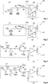
- the figure 9 is an electrical diagram illustrating an example of an optical and thermal TFT fingerprint sensor 190 according to a second embodiment.
- the sensor 190 of the figure 9 is a load-bearing sensor. This sensor comprises elements common with the sensor 170 of the figure 7 . These elements will not be described again.
- the sensor 190 of the figure 9 differs from the sensor 170 of the figure 7 essentially in that, in the sensor 190, elementary acquisition cells 191 replace the cells 171 of the sensor 170.
- the cells 191 of the sensor 190 differ from the cells 171 of the sensor 170 in that, in the cells 191, the photodetector PS is not connected directly between the nodes GND and SN, but is connected between the node GND and an intermediate node n2, the node n2 being connected to the node SN by a selection transistor SW.
- the pyroelectric element PYR is connected directly to the node SN. More particularly, in this example, the photodetector PS is a photodiode whose anode is connected to the GND node and whose cathode is connected to the node n2.
- the selection transistor SW is connected to both the photodetector PS and the pyroelectric element PYR.
- the read transistor RS of the cell is shared by the photodetector PS and the pyroelectric element PYR.
- the transistors SW make it possible, in each elementary acquisition cell, to isolate the photodetector PS from the rest of the cell.
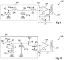
- the figure 10 is an electrical diagram illustrating another example of an optical and thermal TFT fingerprint sensor 200 according to the second embodiment.
- the sensor 200 of the figure 10 is a voltage reading sensor. This sensor comprises elements that are common with the sensor 160 of the figure 6 . These elements will not be described again.
- the sensor 200 of the figure 10 differs from the sensor 160 of the figure 6 essentially in that, in the sensor 200, elementary acquisition cells 201 replace the cells 161 of the sensor 160.
- the cells 201 of the sensor 200 differ from the cells 161 of the sensor 160 in that, in the cells 201, the PS photodetector is not connected directly between the nodes GND and SN, but is connected between the node GND and an intermediate node n3, the node n3 being connected to the node SN by a selection transistor SW.
- the pyroelectric element PYR is connected directly to the node SN. More particularly, in this example, the photodetector PS is a photodiode whose anode is connected to the GND node and whose cathode is connected to the node n3.
- the selection transistor SW is connected to both the photodetector PS and the pyroelectric element PYR.
- the transistors RT, SF and RD of the cell are shared by the photodetector PS and the pyroelectric element PYR.
- the transistors SW make it possible, in each elementary acquisition cell, to isolate the photodetector PS from the rest of the cell, which offers additional control possibilities with respect to the sensor 160 of the figure 6 , all limiting the cost and bulk compared to a sensor with two selection transistors SW1 and SW2 per cell, of the type described in connection with the figure 5 .
- this gives more flexibility in the dimensioning of PS and thermal conversion elements PYR, than in a sensor of the type described in connection with the figure 6 .
- the photodetector PS and the pyroelectric element PYR can be interchanged, that is to say that the PYR element can be placed behind the selection transistor SW, between the node n2 or n3 and the node GND, the photodetector PS being then directly connected to the SN node.
- This choice can be made according to the respective values of the capacities of the PYR and PS elements.
- the photodetector can generate, in addition to the useful signal representative of the pattern of the print to be acquired, noise associated in particular with the currents of darkness and / or light. room.
- the source of light so as to acquire an image representative of the noise generated by the photodetector PS (particularly related to dark currents and parasitic ambient light). Once this image is acquired, it can be subtracted from the final optical image, and, if the photodetector is not isolated from the pyroelectric element, to the final thermal image.
- thermal and optical instead of performing two separate readings, thermal and optical, respectively, seeking to distinguish the thermal signal from the optical signal, as described above, it is possible to read the sum of the photogenerated charges and charges generated by the pyroelectric element, without seeking to separate them, in order to acquire an image combining the optical signal and the thermal signal, which can prove useful for acquiring certain difficult footprints.
- control method in which, during the acquisition of a print, an optical image and a thermal image are read, may be provided for embodiments in which reads several optical images and / or several thermal images of the same footprint.
- the optical integration period is several times greater than the time required to implement the steps of thermal reading of all lines of the sensor, it can be expected to scan successively several times all sensor to acquire several thermal images, then, at the last scan of the sensor, to acquire the optical image.
- the embodiments described above can be combined with other fingerprint acquisition technologies, for example ultrasonic or electric field acquisition technologies, or technologies in which an RF signal is applied through the skin of the user.
- the temperature variation exploited by the PYR pyroelectric conversion elements is a variation that occurs when the user places his finger on the sensor, and / or removes it from the sensor.
- Such sensors can be of static type (the surface of the sensor is at least equal to the surface of the impression to be acquired, and the finger does not move relative to the sensor during the acquisition) or of scanning type (the surface the sensor is smaller than the area of the impression to be acquired, and the finger scrolls past the sensor during acquisition).
Claims (11)
- Ein Finger- oder Handabdrucksensor (150; 160; 170; 180; 190; 200), der Folgendes aufweist:auf einem Trägersubstrat eine Vielzahl von elementaren Erfassungszellen (151; 161; 171; 181; 191; 201), die in TFT-Technologie realisiert sind, wobei jede Zelle einen Fotodetektor (PS) und ein pyroelektrisches Umwandlungselement (PYR) aufweist, das an einen gleichen kapazitiven Sensorknoten (SN) der Zelle gekoppelt ist, und eine Ausleseschaltung (RS; SF, RD), die den kapazitiven Sensorknoten (SN) der Zelle an eine Ausgangsleiterbahn (CL) der Zelle koppelt;eine Beleuchtungslichtquelle; undeine Wärmequelle, die sich von der Lichtquelle unterscheidet.
- Sensor (150; 160; 170; 180; 190; 200) nach Anspruch 1, wobei das Trägersubstrat transparent ist.
- Sensor (160; 170; 180) nach Anspruch 1 oder 2, wobei der Fotodetektor (PS) und das pyroelektrische Umwandlungselement (PYR) parallel geschaltet sind.
- Sensor (160; 170; 180) nach einem der Ansprüche 1 bis 3, der eine Schaltung aufweist, die geeignet ist zum Steuern der Erfassung eines thermischen Bildes und der Erfassung eines optischen Bildes durch die Sensorzellen (161; 171; 181), wobei die Schaltung geeignet ist, während der gesamten optischen Bilderfassungsphase die Lichtquelle einzuschalten und die Wärmequelle ausgeschaltet zu halten und während der gesamten thermischen Bilderfassungsphase die Lichtquelle ausgeschaltet zu halten.
- Sensor (160; 170; 180) nach einem der Ansprüche 1 bis 3, der eine Schaltung aufweist, die geeignet ist zum Steuern der Erfassung eines thermischen Bildes und der Erfassung eines optischen Bildes durch die Sensorzellen (161; 171; 181), wobei die Schaltung geeignet ist zum Implementieren der Erfassung des thermischen Bildes während einem Teil einer Integrationsdauer der optischen Bilderfassungsphase während der die Lichtquelle an ist.
- Sensor (160; 170) nach einem der Ansprüche 1 bis 5, wobei in jeder Zelle (161; 171) der Fotodetektor (PS) und das pyroelektrische Umwandlungselement (PYR) an den kapazitiven Sensorknoten (SN) der Zelle gekoppelt sind.
- Sensor (180) nach einem der Ansprüche 1 bis 5, wobei in jeder Zelle (181) der Fotodetektor (PS) und das pyroelektrische Umwandlungselement (PYR) an einen Zwischenknoten (n1) der Zelle gekoppelt sind, wobei der Zwischenknoten an den kapazitiven Sensorknoten (SN) der Zelle durch einen Auswahltransistor (SW) gekoppelt ist und jede Zelle (181) ferner Folgendes aufweist:einen Referenzkondensator (CREF), der zwischen dem kapazitiven Sensorknoten (SN) und einem Knoten (CMD) des Anlegens eines Kontrollsignals verbunden ist; undeine Elektrode (EL), die mit dem kapazitiven Sensorknoten (SN) verbunden ist, wobei die Elektrode (EL) mit einer dielektrischen Schicht beschichtet ist und bestimmt ist zum Bilden einer Kapazität mit der Haut eines Nutzers zur kapazitiven Erfassung eines Abdruckbildes.
- Sensor (190; 200) nach Anspruch 1 oder 2, wobei der Fotodetektor (PS) und das pyroelektrische Umwandlungselement (PYR) mit einem gleichen Selektionstransistor (SW) verbunden sind, um in dem Auszustand zu ermöglichen, den Fotodetektor (PS) von dem pyroelektrischen Element (PYR) zu isolieren.
- Sensor (150; 160; 170; 180; 190; 200) nach einem der Ansprüche 1 bis 8, wobei die Zellen (151; 161; 171; 181; 191; 201) in einer Reihen- und Spaltenanordnung angeordnet sind und wobei die Wärmequelle zum Erwärmen der Zellen (151; 161; 171; 181; 191; 201) Reihe für Reihe steuerbar ist.
- Sensor (150; 160; 180; 200) nach einem der Ansprüche 1 bis 9, wobei die Zellen (151; 161; 181; 201) Spannungsauslesezellen sind, wobei jede Zelle einen Reset-Transistor (RT) aufweist, der den kapazitiven Sensorknoten (SN) an einen Knoten (VRT) des Anlegens eines Reset-Potentials koppelt und die Ausleseschaltung jeder Zelle einen Transistor (SF), der als eine Folgequelle angeordnet ist, aufweist, dessen Gatter mit dem Sensorknoten (SN) verbunden ist und dessen Quelle mit einer Ausgangsbahn (CL) der Zelle über einen Auslesetransistor (RD) verbunden ist.
- Sensor (170; 190) nach einem der Ansprüche 1 bis 9, wobei die Zellen (171; 191) Ladeauslesezellen sind, wobei die Ausleseschaltung jeder Zelle einen Auslesetransistor (RS) aufweist, der den Sensorknoten (SN) an die Ausgangsbahn (CL) jeder Zelle koppelt.
Applications Claiming Priority (2)
| Application Number | Priority Date | Filing Date | Title |
|---|---|---|---|
| FR1459494A FR3026877B1 (fr) | 2014-10-03 | 2014-10-03 | Capteur d'empreintes digitales ou palmaires |
| PCT/FR2015/052616 WO2016051087A1 (fr) | 2014-10-03 | 2015-09-30 | Capteur d'empreintes digitales ou palmaires |
Publications (2)
| Publication Number | Publication Date |
|---|---|
| EP3201832A1 EP3201832A1 (de) | 2017-08-09 |
| EP3201832B1 true EP3201832B1 (de) | 2018-10-10 |
Family
ID=52465481
Family Applications (1)
| Application Number | Title | Priority Date | Filing Date |
|---|---|---|---|
| EP15788117.8A Active EP3201832B1 (de) | 2014-10-03 | 2015-09-30 | Fingerabdruck- oder handflächensensor |
Country Status (7)
| Country | Link |
|---|---|
| US (1) | US10176357B2 (de) |
| EP (1) | EP3201832B1 (de) |
| JP (1) | JP6741657B2 (de) |
| KR (1) | KR20170104439A (de) |
| CN (1) | CN107004125B (de) |
| FR (1) | FR3026877B1 (de) |
| WO (1) | WO2016051087A1 (de) |
Families Citing this family (47)
| Publication number | Priority date | Publication date | Assignee | Title |
|---|---|---|---|---|
| CN104915657B (zh) * | 2015-06-29 | 2018-09-18 | 京东方科技集团股份有限公司 | 基于ltps技术的掌纹识别电路、掌纹识别方法以及显示屏 |
| FR3046277B1 (fr) * | 2015-12-23 | 2018-02-16 | Commissariat A L'energie Atomique Et Aux Energies Alternatives | Procede pour reconnaitre une fausse empreinte papillaire par eclairage structure |
| CN105631432B (zh) * | 2016-01-04 | 2020-12-08 | 京东方科技集团股份有限公司 | 指纹探测电路及驱动方法和显示装置 |
| US10315222B2 (en) | 2016-05-04 | 2019-06-11 | Invensense, Inc. | Two-dimensional array of CMOS control elements |
| US10656255B2 (en) | 2016-05-04 | 2020-05-19 | Invensense, Inc. | Piezoelectric micromachined ultrasonic transducer (PMUT) |
| US10670716B2 (en) | 2016-05-04 | 2020-06-02 | Invensense, Inc. | Operating a two-dimensional array of ultrasonic transducers |
| US10325915B2 (en) | 2016-05-04 | 2019-06-18 | Invensense, Inc. | Two-dimensional array of CMOS control elements |
| US10445547B2 (en) | 2016-05-04 | 2019-10-15 | Invensense, Inc. | Device mountable packaging of ultrasonic transducers |
| US10539539B2 (en) | 2016-05-10 | 2020-01-21 | Invensense, Inc. | Operation of an ultrasonic sensor |
| US10452887B2 (en) | 2016-05-10 | 2019-10-22 | Invensense, Inc. | Operating a fingerprint sensor comprised of ultrasonic transducers |
| US10600403B2 (en) | 2016-05-10 | 2020-03-24 | Invensense, Inc. | Transmit operation of an ultrasonic sensor |
| US10562070B2 (en) | 2016-05-10 | 2020-02-18 | Invensense, Inc. | Receive operation of an ultrasonic sensor |
| US10408797B2 (en) | 2016-05-10 | 2019-09-10 | Invensense, Inc. | Sensing device with a temperature sensor |
| US11673165B2 (en) | 2016-05-10 | 2023-06-13 | Invensense, Inc. | Ultrasonic transducer operable in a surface acoustic wave (SAW) mode |
| US10706835B2 (en) | 2016-05-10 | 2020-07-07 | Invensense, Inc. | Transmit beamforming of a two-dimensional array of ultrasonic transducers |
| US10441975B2 (en) | 2016-05-10 | 2019-10-15 | Invensense, Inc. | Supplemental sensor modes and systems for ultrasonic transducers |
| US10632500B2 (en) | 2016-05-10 | 2020-04-28 | Invensense, Inc. | Ultrasonic transducer with a non-uniform membrane |
| FR3054698B1 (fr) * | 2016-07-29 | 2018-09-28 | Commissariat A L'energie Atomique Et Aux Energies Alternatives | Capteur de motif thermique actif comprenant une matrice passive de pixels |
| US10162462B2 (en) * | 2017-05-01 | 2018-12-25 | Synaptics Incorporated | Integrating capacitive sensing with an optical sensor |
| US10891461B2 (en) | 2017-05-22 | 2021-01-12 | Invensense, Inc. | Live fingerprint detection utilizing an integrated ultrasound and infrared sensor |
| US10474862B2 (en) | 2017-06-01 | 2019-11-12 | Invensense, Inc. | Image generation in an electronic device using ultrasonic transducers |
| US10643052B2 (en) | 2017-06-28 | 2020-05-05 | Invensense, Inc. | Image generation in an electronic device using ultrasonic transducers |
| US10936841B2 (en) | 2017-12-01 | 2021-03-02 | Invensense, Inc. | Darkfield tracking |
| US10984209B2 (en) | 2017-12-01 | 2021-04-20 | Invensense, Inc. | Darkfield modeling |
| US10997388B2 (en) | 2017-12-01 | 2021-05-04 | Invensense, Inc. | Darkfield contamination detection |
| FR3075954B1 (fr) * | 2017-12-22 | 2020-01-10 | Commissariat A L'energie Atomique Et Aux Energies Alternatives | Capteur pyroelectrique avec blindage electro-magnetique comprenant un materiau composite. |
| US11151355B2 (en) | 2018-01-24 | 2021-10-19 | Invensense, Inc. | Generation of an estimated fingerprint |
| TWI652625B (zh) | 2018-03-16 | 2019-03-01 | 友達光電股份有限公司 | 指紋感測裝置 |
| US10755067B2 (en) | 2018-03-22 | 2020-08-25 | Invensense, Inc. | Operating a fingerprint sensor comprised of ultrasonic transducers |
| US10937835B2 (en) | 2018-11-21 | 2021-03-02 | BAE Systems Imaging Solutions Inc. | Low-noise integrated post-processed photodiode |
| US10936843B2 (en) | 2018-12-28 | 2021-03-02 | Invensense, Inc. | Segmented image acquisition |
| CN111404533B (zh) * | 2019-01-02 | 2022-06-03 | 京东方科技集团股份有限公司 | 检测电路、纹路识别装置及驱动方法 |
| CN110135348B (zh) * | 2019-05-15 | 2021-02-09 | 京东方科技集团股份有限公司 | 指纹检测电路及其驱动方法、阵列基板、显示装置 |
| CN110287808B (zh) * | 2019-06-03 | 2022-01-14 | 京东方科技集团股份有限公司 | 阵列基板及其制造方法,以及显示面板和显示装置 |
| WO2020263875A1 (en) | 2019-06-24 | 2020-12-30 | Invensense, Inc. | Fake finger detection using ridge features |
| WO2020264046A1 (en) | 2019-06-25 | 2020-12-30 | Invensense, Inc. | Fake finger detection based on transient features |
| US11176345B2 (en) | 2019-07-17 | 2021-11-16 | Invensense, Inc. | Ultrasonic fingerprint sensor with a contact layer of non-uniform thickness |
| US11216632B2 (en) | 2019-07-17 | 2022-01-04 | Invensense, Inc. | Ultrasonic fingerprint sensor with a contact layer of non-uniform thickness |
| US11232549B2 (en) | 2019-08-23 | 2022-01-25 | Invensense, Inc. | Adapting a quality threshold for a fingerprint image |
| US20220004729A1 (en) * | 2019-08-29 | 2022-01-06 | Boe Technology Group Co., Ltd. | Fingerprint identification circuit and driving method thereof, fingerprint identification module, and display device |
| US11392789B2 (en) | 2019-10-21 | 2022-07-19 | Invensense, Inc. | Fingerprint authentication using a synthetic enrollment image |
| EP4100176A1 (de) | 2020-03-09 | 2022-12-14 | InvenSense, Inc. | Ultraschall-fingerabdrucksensor mit einer kontaktschicht uneinheitlicher dicke |
| US11243300B2 (en) | 2020-03-10 | 2022-02-08 | Invensense, Inc. | Operating a fingerprint sensor comprised of ultrasonic transducers and a presence sensor |
| US11328165B2 (en) | 2020-04-24 | 2022-05-10 | Invensense, Inc. | Pressure-based activation of fingerprint spoof detection |
| CN112699853B (zh) * | 2021-01-28 | 2024-02-02 | 合肥维信诺科技有限公司 | 指纹识别电路及其驱动方法、指纹识别设备 |
| US11380126B1 (en) * | 2021-02-04 | 2022-07-05 | Himax Technologies Limited | Display device with embedded biometric detection function in active region |
| US11886666B1 (en) * | 2022-08-08 | 2024-01-30 | Himax Technologies Limited | Fingerprint detection system and a detection circuit adaptable thereto |
Family Cites Families (13)
| Publication number | Priority date | Publication date | Assignee | Title |
|---|---|---|---|---|
| GB1105828A (en) | 1964-12-14 | 1968-03-13 | Allied Chem | Fumaric acid beverage mixes |
| JPH1079499A (ja) * | 1996-09-05 | 1998-03-24 | Nikon Corp | 受光素子およびこれを用いたイメージセンサ |
| GB9804539D0 (en) * | 1998-03-05 | 1998-04-29 | Philips Electronics Nv | Fingerprint sensing devices and systems incorporating such |
| FR2781927B1 (fr) * | 1998-07-28 | 2001-10-05 | Commissariat Energie Atomique | Dispositif de detection de rayonnements multispectraux infrarouge/visible |
| JP3559754B2 (ja) * | 2000-07-25 | 2004-09-02 | Necエレクトロニクス株式会社 | 指紋認証装置 |
| US7088443B2 (en) * | 2002-02-11 | 2006-08-08 | Kla-Tencor Technologies Corporation | System for detecting anomalies and/or features of a surface |
| JP2006343229A (ja) * | 2005-06-09 | 2006-12-21 | Mitsubishi Electric Corp | イメージセンサ |
| KR101473424B1 (ko) * | 2010-06-01 | 2014-12-24 | 볼리 미디어 커뮤니케이션스 (센젠) 캄파니 리미티드 | 다중 스펙트럼 감광소자 및 그 샘플링 방법 |
| US20120321149A1 (en) * | 2011-05-17 | 2012-12-20 | Carver John F | Fingerprint sensors |
| CN103136507A (zh) * | 2011-11-26 | 2013-06-05 | 陈亘朝 | 指纹形混合识别装置 |
| FR2999338B1 (fr) * | 2012-12-10 | 2017-12-08 | Soc Fr De Detecteurs Infrarouges - Sofradir | Imageur monolithique multispectral visible et infrarouge |
| US9798372B2 (en) * | 2013-06-03 | 2017-10-24 | Qualcomm Incorporated | Devices and methods of sensing combined ultrasonic and infrared signal |
| KR101376228B1 (ko) * | 2013-07-17 | 2014-04-01 | 실리콘 디스플레이 (주) | 광학식 및 정전용량방식으로 지문인식이 가능한 지문인식센서 |
-
2014
- 2014-10-03 FR FR1459494A patent/FR3026877B1/fr active Active
-
2015
- 2015-09-30 CN CN201580065747.8A patent/CN107004125B/zh active Active
- 2015-09-30 KR KR1020177011066A patent/KR20170104439A/ko not_active Application Discontinuation
- 2015-09-30 JP JP2017518055A patent/JP6741657B2/ja active Active
- 2015-09-30 US US15/516,402 patent/US10176357B2/en active Active
- 2015-09-30 EP EP15788117.8A patent/EP3201832B1/de active Active
- 2015-09-30 WO PCT/FR2015/052616 patent/WO2016051087A1/fr active Application Filing
Non-Patent Citations (1)
| Title |
|---|
| None * |
Also Published As
| Publication number | Publication date |
|---|---|
| JP6741657B2 (ja) | 2020-08-19 |
| US10176357B2 (en) | 2019-01-08 |
| FR3026877B1 (fr) | 2018-01-05 |
| WO2016051087A1 (fr) | 2016-04-07 |
| JP2017538101A (ja) | 2017-12-21 |
| EP3201832A1 (de) | 2017-08-09 |
| US20170293791A1 (en) | 2017-10-12 |
| CN107004125B (zh) | 2021-06-15 |
| FR3026877A1 (fr) | 2016-04-08 |
| KR20170104439A (ko) | 2017-09-15 |
| CN107004125A (zh) | 2017-08-01 |
Similar Documents
| Publication | Publication Date | Title |
|---|---|---|
| EP3201832B1 (de) | Fingerabdruck- oder handflächensensor | |
| EP3289521B1 (de) | Fingerabdruck- oder handflächensensor | |
| EP3332548B1 (de) | Verfahren zur steuerung eines aktiven pixelbildsensors | |
| EP0237365B1 (de) | Lichtempfindliche Vorrichtung | |
| EP2477393B1 (de) | Bildanzeigevorrichtung mit großem dynamischem Bereich | |
| FR2593343A1 (fr) | Matrice d'elements photosensibles et son procede de fabrication, procede de lecture associe, et application de cette matrice a la prise de vue d'images | |
| CA2760468C (fr) | Systeme et procede de detection de rayonnement infrarouge | |
| CA2632505C (fr) | Dispositif de detection de rayonnement infrarouge a detecteurs bolometriques | |
| FR2598250A1 (fr) | Panneau de prise de vue radiologique, et procede de fabrication | |
| EP3931872A1 (de) | Farb- und infrarotbildsensor | |
| EP1796373A1 (de) | Abbildungsverfahren mit Hilfe eines Bildsensors mit grossem dynamik Bereich | |
| EP3767679B1 (de) | Pixel eines bildsensors | |
| EP3069506B1 (de) | Pooling von zwei pixelspalten eines bilddetektors | |
| EP3289522B1 (de) | Pyroelektrischer sensor zum nachweis von hautabdrücken | |
| WO2015028672A1 (fr) | Capteur d'image avec bruit ktc reduit | |
| EP0749234B1 (de) | Halbleiter-Bildsensor mit integrierte Pixelhistogrammumwandlung | |
| EP3767677A1 (de) | Pixel eines bildsensors | |
| EP3767260A1 (de) | Sensor und verfahren zur erfassung eines wärmemusters mit doppelter integration | |
| EP3767678A1 (de) | Pixel eines bildsensors | |
| WO2021043456A1 (fr) | Capteur infrarouge a capture instantanee | |
| EP0818827A1 (de) | Fotodetektor mit verbesserter Reaktionszeit und Sensormatrix mit einer Vielzahl von Fotodetektoren | |
| FR2941329A1 (fr) | Detecteur bispectral. |
Legal Events
| Date | Code | Title | Description |
|---|---|---|---|
| STAA | Information on the status of an ep patent application or granted ep patent |
Free format text: STATUS: THE INTERNATIONAL PUBLICATION HAS BEEN MADE |
|
| PUAI | Public reference made under article 153(3) epc to a published international application that has entered the european phase |
Free format text: ORIGINAL CODE: 0009012 |
|
| STAA | Information on the status of an ep patent application or granted ep patent |
Free format text: STATUS: REQUEST FOR EXAMINATION WAS MADE |
|
| 17P | Request for examination filed |
Effective date: 20170329 |
|
| AK | Designated contracting states |
Kind code of ref document: A1 Designated state(s): AL AT BE BG CH CY CZ DE DK EE ES FI FR GB GR HR HU IE IS IT LI LT LU LV MC MK MT NL NO PL PT RO RS SE SI SK SM TR |
|
| AX | Request for extension of the european patent |
Extension state: BA ME |
|
| DAV | Request for validation of the european patent (deleted) | ||
| DAX | Request for extension of the european patent (deleted) | ||
| RAP1 | Party data changed (applicant data changed or rights of an application transferred) |
Owner name: COMMISSARIAT A L'ENERGIE ATOMIQUE ET AUX ENERGIES Owner name: SAFRAN IDENTITY & SECURITY |
|
| GRAP | Despatch of communication of intention to grant a patent |
Free format text: ORIGINAL CODE: EPIDOSNIGR1 |
|
| STAA | Information on the status of an ep patent application or granted ep patent |
Free format text: STATUS: GRANT OF PATENT IS INTENDED |
|
| INTG | Intention to grant announced |
Effective date: 20180614 |
|
| GRAS | Grant fee paid |
Free format text: ORIGINAL CODE: EPIDOSNIGR3 |
|
| GRAA | (expected) grant |
Free format text: ORIGINAL CODE: 0009210 |
|
| STAA | Information on the status of an ep patent application or granted ep patent |
Free format text: STATUS: THE PATENT HAS BEEN GRANTED |
|
| AK | Designated contracting states |
Kind code of ref document: B1 Designated state(s): AL AT BE BG CH CY CZ DE DK EE ES FI FR GB GR HR HU IE IS IT LI LT LU LV MC MK MT NL NO PL PT RO RS SE SI SK SM TR |
|
| REG | Reference to a national code |
Ref country code: GB Ref legal event code: FG4D Free format text: NOT ENGLISH |
|
| REG | Reference to a national code |
Ref country code: CH Ref legal event code: EP Ref country code: AT Ref legal event code: REF Ref document number: 1052105 Country of ref document: AT Kind code of ref document: T Effective date: 20181015 |
|
| REG | Reference to a national code |
Ref country code: IE Ref legal event code: FG4D Free format text: LANGUAGE OF EP DOCUMENT: FRENCH |
|
| REG | Reference to a national code |
Ref country code: DE Ref legal event code: R096 Ref document number: 602015018003 Country of ref document: DE |
|
| RAP2 | Party data changed (patent owner data changed or rights of a patent transferred) |
Owner name: IDEMIA IDENTITY & SECURITY FRANCE Owner name: COMMISSARIAT A L'ENERGIE ATOMIQUE ET AUX ENERGIES |
|
| REG | Reference to a national code |
Ref country code: NL Ref legal event code: MP Effective date: 20181010 |
|
| REG | Reference to a national code |
Ref country code: NO Ref legal event code: T2 Effective date: 20181010 |
|
| REG | Reference to a national code |
Ref country code: LT Ref legal event code: MG4D |
|
| REG | Reference to a national code |
Ref country code: AT Ref legal event code: MK05 Ref document number: 1052105 Country of ref document: AT Kind code of ref document: T Effective date: 20181010 |
|
| PG25 | Lapsed in a contracting state [announced via postgrant information from national office to epo] |
Ref country code: NL Free format text: LAPSE BECAUSE OF FAILURE TO SUBMIT A TRANSLATION OF THE DESCRIPTION OR TO PAY THE FEE WITHIN THE PRESCRIBED TIME-LIMIT Effective date: 20181010 |
|
| PG25 | Lapsed in a contracting state [announced via postgrant information from national office to epo] |
Ref country code: LV Free format text: LAPSE BECAUSE OF FAILURE TO SUBMIT A TRANSLATION OF THE DESCRIPTION OR TO PAY THE FEE WITHIN THE PRESCRIBED TIME-LIMIT Effective date: 20181010 Ref country code: ES Free format text: LAPSE BECAUSE OF FAILURE TO SUBMIT A TRANSLATION OF THE DESCRIPTION OR TO PAY THE FEE WITHIN THE PRESCRIBED TIME-LIMIT Effective date: 20181010 Ref country code: LT Free format text: LAPSE BECAUSE OF FAILURE TO SUBMIT A TRANSLATION OF THE DESCRIPTION OR TO PAY THE FEE WITHIN THE PRESCRIBED TIME-LIMIT Effective date: 20181010 Ref country code: IS Free format text: LAPSE BECAUSE OF FAILURE TO SUBMIT A TRANSLATION OF THE DESCRIPTION OR TO PAY THE FEE WITHIN THE PRESCRIBED TIME-LIMIT Effective date: 20190210 Ref country code: AT Free format text: LAPSE BECAUSE OF FAILURE TO SUBMIT A TRANSLATION OF THE DESCRIPTION OR TO PAY THE FEE WITHIN THE PRESCRIBED TIME-LIMIT Effective date: 20181010 Ref country code: FI Free format text: LAPSE BECAUSE OF FAILURE TO SUBMIT A TRANSLATION OF THE DESCRIPTION OR TO PAY THE FEE WITHIN THE PRESCRIBED TIME-LIMIT Effective date: 20181010 Ref country code: BG Free format text: LAPSE BECAUSE OF FAILURE TO SUBMIT A TRANSLATION OF THE DESCRIPTION OR TO PAY THE FEE WITHIN THE PRESCRIBED TIME-LIMIT Effective date: 20190110 Ref country code: PL Free format text: LAPSE BECAUSE OF FAILURE TO SUBMIT A TRANSLATION OF THE DESCRIPTION OR TO PAY THE FEE WITHIN THE PRESCRIBED TIME-LIMIT Effective date: 20181010 Ref country code: HR Free format text: LAPSE BECAUSE OF FAILURE TO SUBMIT A TRANSLATION OF THE DESCRIPTION OR TO PAY THE FEE WITHIN THE PRESCRIBED TIME-LIMIT Effective date: 20181010 |
|
| PG25 | Lapsed in a contracting state [announced via postgrant information from national office to epo] |
Ref country code: SE Free format text: LAPSE BECAUSE OF FAILURE TO SUBMIT A TRANSLATION OF THE DESCRIPTION OR TO PAY THE FEE WITHIN THE PRESCRIBED TIME-LIMIT Effective date: 20181010 Ref country code: AL Free format text: LAPSE BECAUSE OF FAILURE TO SUBMIT A TRANSLATION OF THE DESCRIPTION OR TO PAY THE FEE WITHIN THE PRESCRIBED TIME-LIMIT Effective date: 20181010 Ref country code: PT Free format text: LAPSE BECAUSE OF FAILURE TO SUBMIT A TRANSLATION OF THE DESCRIPTION OR TO PAY THE FEE WITHIN THE PRESCRIBED TIME-LIMIT Effective date: 20190210 Ref country code: RS Free format text: LAPSE BECAUSE OF FAILURE TO SUBMIT A TRANSLATION OF THE DESCRIPTION OR TO PAY THE FEE WITHIN THE PRESCRIBED TIME-LIMIT Effective date: 20181010 Ref country code: GR Free format text: LAPSE BECAUSE OF FAILURE TO SUBMIT A TRANSLATION OF THE DESCRIPTION OR TO PAY THE FEE WITHIN THE PRESCRIBED TIME-LIMIT Effective date: 20190111 |
|
| REG | Reference to a national code |
Ref country code: DE Ref legal event code: R097 Ref document number: 602015018003 Country of ref document: DE |
|
| PG25 | Lapsed in a contracting state [announced via postgrant information from national office to epo] |
Ref country code: DK Free format text: LAPSE BECAUSE OF FAILURE TO SUBMIT A TRANSLATION OF THE DESCRIPTION OR TO PAY THE FEE WITHIN THE PRESCRIBED TIME-LIMIT Effective date: 20181010 Ref country code: CZ Free format text: LAPSE BECAUSE OF FAILURE TO SUBMIT A TRANSLATION OF THE DESCRIPTION OR TO PAY THE FEE WITHIN THE PRESCRIBED TIME-LIMIT Effective date: 20181010 Ref country code: IT Free format text: LAPSE BECAUSE OF FAILURE TO SUBMIT A TRANSLATION OF THE DESCRIPTION OR TO PAY THE FEE WITHIN THE PRESCRIBED TIME-LIMIT Effective date: 20181010 |
|
| PLBE | No opposition filed within time limit |
Free format text: ORIGINAL CODE: 0009261 |
|
| STAA | Information on the status of an ep patent application or granted ep patent |
Free format text: STATUS: NO OPPOSITION FILED WITHIN TIME LIMIT |
|
| PG25 | Lapsed in a contracting state [announced via postgrant information from national office to epo] |
Ref country code: RO Free format text: LAPSE BECAUSE OF FAILURE TO SUBMIT A TRANSLATION OF THE DESCRIPTION OR TO PAY THE FEE WITHIN THE PRESCRIBED TIME-LIMIT Effective date: 20181010 Ref country code: EE Free format text: LAPSE BECAUSE OF FAILURE TO SUBMIT A TRANSLATION OF THE DESCRIPTION OR TO PAY THE FEE WITHIN THE PRESCRIBED TIME-LIMIT Effective date: 20181010 Ref country code: SM Free format text: LAPSE BECAUSE OF FAILURE TO SUBMIT A TRANSLATION OF THE DESCRIPTION OR TO PAY THE FEE WITHIN THE PRESCRIBED TIME-LIMIT Effective date: 20181010 Ref country code: SK Free format text: LAPSE BECAUSE OF FAILURE TO SUBMIT A TRANSLATION OF THE DESCRIPTION OR TO PAY THE FEE WITHIN THE PRESCRIBED TIME-LIMIT Effective date: 20181010 |
|
| 26N | No opposition filed |
Effective date: 20190711 |
|
| PG25 | Lapsed in a contracting state [announced via postgrant information from national office to epo] |
Ref country code: SI Free format text: LAPSE BECAUSE OF FAILURE TO SUBMIT A TRANSLATION OF THE DESCRIPTION OR TO PAY THE FEE WITHIN THE PRESCRIBED TIME-LIMIT Effective date: 20181010 |
|
| PG25 | Lapsed in a contracting state [announced via postgrant information from national office to epo] |
Ref country code: TR Free format text: LAPSE BECAUSE OF FAILURE TO SUBMIT A TRANSLATION OF THE DESCRIPTION OR TO PAY THE FEE WITHIN THE PRESCRIBED TIME-LIMIT Effective date: 20181010 |
|
| PG25 | Lapsed in a contracting state [announced via postgrant information from national office to epo] |
Ref country code: MC Free format text: LAPSE BECAUSE OF FAILURE TO SUBMIT A TRANSLATION OF THE DESCRIPTION OR TO PAY THE FEE WITHIN THE PRESCRIBED TIME-LIMIT Effective date: 20181010 |
|
| REG | Reference to a national code |
Ref country code: CH Ref legal event code: PL |
|
| PG25 | Lapsed in a contracting state [announced via postgrant information from national office to epo] |
Ref country code: LI Free format text: LAPSE BECAUSE OF NON-PAYMENT OF DUE FEES Effective date: 20190930 Ref country code: CH Free format text: LAPSE BECAUSE OF NON-PAYMENT OF DUE FEES Effective date: 20190930 Ref country code: LU Free format text: LAPSE BECAUSE OF NON-PAYMENT OF DUE FEES Effective date: 20190930 Ref country code: IE Free format text: LAPSE BECAUSE OF NON-PAYMENT OF DUE FEES Effective date: 20190930 |
|
| REG | Reference to a national code |
Ref country code: BE Ref legal event code: MM Effective date: 20190930 |
|
| PG25 | Lapsed in a contracting state [announced via postgrant information from national office to epo] |
Ref country code: BE Free format text: LAPSE BECAUSE OF NON-PAYMENT OF DUE FEES Effective date: 20190930 |
|
| GBPC | Gb: european patent ceased through non-payment of renewal fee |
Effective date: 20190930 |
|
| PG25 | Lapsed in a contracting state [announced via postgrant information from national office to epo] |
Ref country code: GB Free format text: LAPSE BECAUSE OF NON-PAYMENT OF DUE FEES Effective date: 20190930 |
|
| PG25 | Lapsed in a contracting state [announced via postgrant information from national office to epo] |
Ref country code: CY Free format text: LAPSE BECAUSE OF FAILURE TO SUBMIT A TRANSLATION OF THE DESCRIPTION OR TO PAY THE FEE WITHIN THE PRESCRIBED TIME-LIMIT Effective date: 20181010 |
|
| PG25 | Lapsed in a contracting state [announced via postgrant information from national office to epo] |
Ref country code: MT Free format text: LAPSE BECAUSE OF FAILURE TO SUBMIT A TRANSLATION OF THE DESCRIPTION OR TO PAY THE FEE WITHIN THE PRESCRIBED TIME-LIMIT Effective date: 20181010 Ref country code: HU Free format text: LAPSE BECAUSE OF FAILURE TO SUBMIT A TRANSLATION OF THE DESCRIPTION OR TO PAY THE FEE WITHIN THE PRESCRIBED TIME-LIMIT; INVALID AB INITIO Effective date: 20150930 |
|
| REG | Reference to a national code |
Ref country code: DE Ref legal event code: R079 Ref document number: 602015018003 Country of ref document: DE Free format text: PREVIOUS MAIN CLASS: G06K0009000000 Ipc: G06V0010000000 |
|
| PG25 | Lapsed in a contracting state [announced via postgrant information from national office to epo] |
Ref country code: MK Free format text: LAPSE BECAUSE OF FAILURE TO SUBMIT A TRANSLATION OF THE DESCRIPTION OR TO PAY THE FEE WITHIN THE PRESCRIBED TIME-LIMIT Effective date: 20181010 |
|
| PGFP | Annual fee paid to national office [announced via postgrant information from national office to epo] |
Ref country code: NO Payment date: 20220823 Year of fee payment: 8 Ref country code: DE Payment date: 20220818 Year of fee payment: 8 |
|
| PGFP | Annual fee paid to national office [announced via postgrant information from national office to epo] |
Ref country code: FR Payment date: 20220819 Year of fee payment: 8 |