EP3767677A1 - Pixel eines bildsensors - Google Patents
Pixel eines bildsensors Download PDFInfo
- Publication number
- EP3767677A1 EP3767677A1 EP20186097.0A EP20186097A EP3767677A1 EP 3767677 A1 EP3767677 A1 EP 3767677A1 EP 20186097 A EP20186097 A EP 20186097A EP 3767677 A1 EP3767677 A1 EP 3767677A1
- Authority
- EP
- European Patent Office
- Prior art keywords
- pixel
- photodetector
- image sensor
- photodetectors
- organic
- Prior art date
- Legal status (The legal status is an assumption and is not a legal conclusion. Google has not performed a legal analysis and makes no representation as to the accuracy of the status listed.)
- Pending
Links
- 238000000034 method Methods 0.000 claims description 25
- 238000004519 manufacturing process Methods 0.000 claims description 21
- 238000003384 imaging method Methods 0.000 claims description 9
- 238000002329 infrared spectrum Methods 0.000 claims description 6
- 230000001629 suppression Effects 0.000 claims description 6
- 238000001429 visible spectrum Methods 0.000 claims description 3
- 239000010410 layer Substances 0.000 description 124
- 230000036961 partial effect Effects 0.000 description 28
- 239000000463 material Substances 0.000 description 21
- 230000005855 radiation Effects 0.000 description 20
- XLOMVQKBTHCTTD-UHFFFAOYSA-N Zinc monoxide Chemical compound [Zn]=O XLOMVQKBTHCTTD-UHFFFAOYSA-N 0.000 description 18
- 238000000151 deposition Methods 0.000 description 16
- 230000008021 deposition Effects 0.000 description 15
- 238000011084 recovery Methods 0.000 description 14
- PXHVJJICTQNCMI-UHFFFAOYSA-N Nickel Chemical compound [Ni] PXHVJJICTQNCMI-UHFFFAOYSA-N 0.000 description 11
- 239000000203 mixture Substances 0.000 description 11
- 238000002161 passivation Methods 0.000 description 10
- 239000011347 resin Substances 0.000 description 10
- 229920005989 resin Polymers 0.000 description 10
- 229910052581 Si3N4 Inorganic materials 0.000 description 9
- BQCADISMDOOEFD-UHFFFAOYSA-N Silver Chemical compound [Ag] BQCADISMDOOEFD-UHFFFAOYSA-N 0.000 description 9
- 230000010354 integration Effects 0.000 description 9
- 239000004065 semiconductor Substances 0.000 description 9
- HQVNEWCFYHHQES-UHFFFAOYSA-N silicon nitride Chemical compound N12[Si]34N5[Si]62N3[Si]51N64 HQVNEWCFYHHQES-UHFFFAOYSA-N 0.000 description 9
- -1 polyethylene terephthalate Polymers 0.000 description 8
- 239000011787 zinc oxide Substances 0.000 description 8
- 239000010949 copper Substances 0.000 description 7
- 239000004205 dimethyl polysiloxane Substances 0.000 description 7
- 238000005530 etching Methods 0.000 description 7
- 238000005240 physical vapour deposition Methods 0.000 description 7
- 238000000623 plasma-assisted chemical vapour deposition Methods 0.000 description 7
- 229920000435 poly(dimethylsiloxane) Polymers 0.000 description 7
- RYGMFSIKBFXOCR-UHFFFAOYSA-N Copper Chemical compound [Cu] RYGMFSIKBFXOCR-UHFFFAOYSA-N 0.000 description 6
- KDLHZDBZIXYQEI-UHFFFAOYSA-N Palladium Chemical compound [Pd] KDLHZDBZIXYQEI-UHFFFAOYSA-N 0.000 description 6
- 229920002873 Polyethylenimine Polymers 0.000 description 6
- VYPSYNLAJGMNEJ-UHFFFAOYSA-N Silicium dioxide Chemical compound O=[Si]=O VYPSYNLAJGMNEJ-UHFFFAOYSA-N 0.000 description 6
- 229910052782 aluminium Inorganic materials 0.000 description 6
- XAGFODPZIPBFFR-UHFFFAOYSA-N aluminium Chemical compound [Al] XAGFODPZIPBFFR-UHFFFAOYSA-N 0.000 description 6
- 239000011651 chromium Substances 0.000 description 6
- 229940082150 encore Drugs 0.000 description 6
- 239000010931 gold Substances 0.000 description 6
- 229920003229 poly(methyl methacrylate) Polymers 0.000 description 6
- 229920000642 polymer Polymers 0.000 description 6
- 239000004926 polymethyl methacrylate Substances 0.000 description 6
- 230000008569 process Effects 0.000 description 6
- 239000004332 silver Substances 0.000 description 6
- 239000010936 titanium Substances 0.000 description 6
- OKTJSMMVPCPJKN-UHFFFAOYSA-N Carbon Chemical compound [C] OKTJSMMVPCPJKN-UHFFFAOYSA-N 0.000 description 5
- GYHNNYVSQQEPJS-UHFFFAOYSA-N Gallium Chemical compound [Ga] GYHNNYVSQQEPJS-UHFFFAOYSA-N 0.000 description 5
- 238000010586 diagram Methods 0.000 description 5
- 229910052733 gallium Inorganic materials 0.000 description 5
- 238000009413 insulation Methods 0.000 description 5
- 229910052709 silver Inorganic materials 0.000 description 5
- VYZAMTAEIAYCRO-UHFFFAOYSA-N Chromium Chemical compound [Cr] VYZAMTAEIAYCRO-UHFFFAOYSA-N 0.000 description 4
- 239000004642 Polyimide Substances 0.000 description 4
- 229910004298 SiO 2 Inorganic materials 0.000 description 4
- RTAQQCXQSZGOHL-UHFFFAOYSA-N Titanium Chemical compound [Ti] RTAQQCXQSZGOHL-UHFFFAOYSA-N 0.000 description 4
- 238000000231 atomic layer deposition Methods 0.000 description 4
- 229920001577 copolymer Polymers 0.000 description 4
- 229910052802 copper Inorganic materials 0.000 description 4
- 238000005520 cutting process Methods 0.000 description 4
- 239000003822 epoxy resin Substances 0.000 description 4
- 239000004811 fluoropolymer Substances 0.000 description 4
- 229920002313 fluoropolymer Polymers 0.000 description 4
- AMGQUBHHOARCQH-UHFFFAOYSA-N indium;oxotin Chemical compound [In].[Sn]=O AMGQUBHHOARCQH-UHFFFAOYSA-N 0.000 description 4
- 229910052751 metal Inorganic materials 0.000 description 4
- 239000002184 metal Substances 0.000 description 4
- 229910052759 nickel Inorganic materials 0.000 description 4
- 238000000206 photolithography Methods 0.000 description 4
- 229920000647 polyepoxide Polymers 0.000 description 4
- 239000005020 polyethylene terephthalate Substances 0.000 description 4
- 229920000139 polyethylene terephthalate Polymers 0.000 description 4
- 229920001721 polyimide Polymers 0.000 description 4
- 229920000036 polyvinylpyrrolidone Polymers 0.000 description 4
- 235000013855 polyvinylpyrrolidone Nutrition 0.000 description 4
- 239000001267 polyvinylpyrrolidone Substances 0.000 description 4
- 229910052814 silicon oxide Inorganic materials 0.000 description 4
- 238000004528 spin coating Methods 0.000 description 4
- 241000287107 Passer Species 0.000 description 3
- 238000000137 annealing Methods 0.000 description 3
- 238000003486 chemical etching Methods 0.000 description 3
- 229910052804 chromium Inorganic materials 0.000 description 3
- 150000001875 compounds Chemical class 0.000 description 3
- 239000004020 conductor Substances 0.000 description 3
- JAONJTDQXUSBGG-UHFFFAOYSA-N dialuminum;dizinc;oxygen(2-) Chemical compound [O-2].[O-2].[O-2].[O-2].[O-2].[Al+3].[Al+3].[Zn+2].[Zn+2] JAONJTDQXUSBGG-UHFFFAOYSA-N 0.000 description 3
- 238000007647 flexography Methods 0.000 description 3
- 230000014509 gene expression Effects 0.000 description 3
- PCHJSUWPFVWCPO-UHFFFAOYSA-N gold Chemical compound [Au] PCHJSUWPFVWCPO-UHFFFAOYSA-N 0.000 description 3
- 229910052737 gold Inorganic materials 0.000 description 3
- 238000002347 injection Methods 0.000 description 3
- 239000007924 injection Substances 0.000 description 3
- 239000007788 liquid Substances 0.000 description 3
- 239000011159 matrix material Substances 0.000 description 3
- 229920000301 poly(3-hexylthiophene-2,5-diyl) polymer Polymers 0.000 description 3
- 239000011112 polyethylene naphthalate Substances 0.000 description 3
- 238000007639 printing Methods 0.000 description 3
- 239000002096 quantum dot Substances 0.000 description 3
- 238000007650 screen-printing Methods 0.000 description 3
- 238000004544 sputter deposition Methods 0.000 description 3
- 229910052719 titanium Inorganic materials 0.000 description 3
- 238000002834 transmittance Methods 0.000 description 3
- 229910052725 zinc Inorganic materials 0.000 description 3
- 239000011701 zinc Substances 0.000 description 3
- PDQRQJVPEFGVRK-UHFFFAOYSA-N 2,1,3-benzothiadiazole Chemical compound C1=CC=CC2=NSN=C21 PDQRQJVPEFGVRK-UHFFFAOYSA-N 0.000 description 2
- 239000005964 Acibenzolar-S-methyl Substances 0.000 description 2
- 239000004925 Acrylic resin Substances 0.000 description 2
- 229910018072 Al 2 O 3 Inorganic materials 0.000 description 2
- ZOKXTWBITQBERF-UHFFFAOYSA-N Molybdenum Chemical compound [Mo] ZOKXTWBITQBERF-UHFFFAOYSA-N 0.000 description 2
- 239000004793 Polystyrene Substances 0.000 description 2
- NRTOMJZYCJJWKI-UHFFFAOYSA-N Titanium nitride Chemical compound [Ti]#N NRTOMJZYCJJWKI-UHFFFAOYSA-N 0.000 description 2
- HCHKCACWOHOZIP-UHFFFAOYSA-N Zinc Chemical compound [Zn] HCHKCACWOHOZIP-UHFFFAOYSA-N 0.000 description 2
- MCEWYIDBDVPMES-UHFFFAOYSA-N [60]pcbm Chemical compound C123C(C4=C5C6=C7C8=C9C%10=C%11C%12=C%13C%14=C%15C%16=C%17C%18=C(C=%19C=%20C%18=C%18C%16=C%13C%13=C%11C9=C9C7=C(C=%20C9=C%13%18)C(C7=%19)=C96)C6=C%11C%17=C%15C%13=C%15C%14=C%12C%12=C%10C%10=C85)=C9C7=C6C2=C%11C%13=C2C%15=C%12C%10=C4C23C1(CCCC(=O)OC)C1=CC=CC=C1 MCEWYIDBDVPMES-UHFFFAOYSA-N 0.000 description 2
- 239000004676 acrylonitrile butadiene styrene Substances 0.000 description 2
- 230000006978 adaptation Effects 0.000 description 2
- 229920000109 alkoxy-substituted poly(p-phenylene vinylene) Polymers 0.000 description 2
- 239000004411 aluminium Substances 0.000 description 2
- 230000008901 benefit Effects 0.000 description 2
- 238000004140 cleaning Methods 0.000 description 2
- 229920001940 conductive polymer Polymers 0.000 description 2
- 238000001312 dry etching Methods 0.000 description 2
- 230000005670 electromagnetic radiation Effects 0.000 description 2
- 238000011156 evaluation Methods 0.000 description 2
- 230000008020 evaporation Effects 0.000 description 2
- 238000001704 evaporation Methods 0.000 description 2
- 229910021389 graphene Inorganic materials 0.000 description 2
- 229910010272 inorganic material Inorganic materials 0.000 description 2
- 239000011147 inorganic material Substances 0.000 description 2
- JEIPFZHSYJVQDO-UHFFFAOYSA-N iron(III) oxide Inorganic materials O=[Fe]O[Fe]=O JEIPFZHSYJVQDO-UHFFFAOYSA-N 0.000 description 2
- 239000007769 metal material Substances 0.000 description 2
- 239000012044 organic layer Substances 0.000 description 2
- 239000011368 organic material Substances 0.000 description 2
- TWNQGVIAIRXVLR-UHFFFAOYSA-N oxo(oxoalumanyloxy)alumane Chemical compound O=[Al]O[Al]=O TWNQGVIAIRXVLR-UHFFFAOYSA-N 0.000 description 2
- 229910052763 palladium Inorganic materials 0.000 description 2
- 230000010287 polarization Effects 0.000 description 2
- 229920003207 poly(ethylene-2,6-naphthalate) Polymers 0.000 description 2
- 229920000052 poly(p-xylylene) Polymers 0.000 description 2
- 239000002094 self assembled monolayer Substances 0.000 description 2
- 239000013545 self-assembled monolayer Substances 0.000 description 2
- 229920002050 silicone resin Polymers 0.000 description 2
- 239000002356 single layer Substances 0.000 description 2
- 238000005507 spraying Methods 0.000 description 2
- 239000012780 transparent material Substances 0.000 description 2
- 238000001039 wet etching Methods 0.000 description 2
- PMGXPAVHYDEYMB-UHFFFAOYSA-N 2-ethyl-1-thieno[2,3-c]thiophen-4-ylhexan-1-one Chemical compound S1C=CC2=C(C(=O)C(CC)CCCC)SC=C21 PMGXPAVHYDEYMB-UHFFFAOYSA-N 0.000 description 1
- NUCIQEWGTLOQTR-UHFFFAOYSA-N 4,4-bis(2-ethylhexyl)-4h-cyclopenta[1,2-b:5,4-b']dithiophene Chemical compound S1C=CC2=C1C(SC=C1)=C1C2(CC(CC)CCCC)CC(CC)CCCC NUCIQEWGTLOQTR-UHFFFAOYSA-N 0.000 description 1
- 229910001316 Ag alloy Inorganic materials 0.000 description 1
- XMWRBQBLMFGWIX-UHFFFAOYSA-N C60 fullerene Chemical class C12=C3C(C4=C56)=C7C8=C5C5=C9C%10=C6C6=C4C1=C1C4=C6C6=C%10C%10=C9C9=C%11C5=C8C5=C8C7=C3C3=C7C2=C1C1=C2C4=C6C4=C%10C6=C9C9=C%11C5=C5C8=C3C3=C7C1=C1C2=C4C6=C2C9=C5C3=C12 XMWRBQBLMFGWIX-UHFFFAOYSA-N 0.000 description 1
- FYYHWMGAXLPEAU-UHFFFAOYSA-N Magnesium Chemical compound [Mg] FYYHWMGAXLPEAU-UHFFFAOYSA-N 0.000 description 1
- 229910000861 Mg alloy Inorganic materials 0.000 description 1
- 229920000144 PEDOT:PSS Polymers 0.000 description 1
- XUIMIQQOPSSXEZ-UHFFFAOYSA-N Silicon Chemical compound [Si] XUIMIQQOPSSXEZ-UHFFFAOYSA-N 0.000 description 1
- 241000897276 Termes Species 0.000 description 1
- ATJFFYVFTNAWJD-UHFFFAOYSA-N Tin Chemical compound [Sn] ATJFFYVFTNAWJD-UHFFFAOYSA-N 0.000 description 1
- 238000010521 absorption reaction Methods 0.000 description 1
- 239000000654 additive Substances 0.000 description 1
- 230000000996 additive effect Effects 0.000 description 1
- 229910045601 alloy Inorganic materials 0.000 description 1
- 239000000956 alloy Substances 0.000 description 1
- PNEYBMLMFCGWSK-UHFFFAOYSA-N aluminium oxide Inorganic materials [O-2].[O-2].[O-2].[Al+3].[Al+3] PNEYBMLMFCGWSK-UHFFFAOYSA-N 0.000 description 1
- JYMITAMFTJDTAE-UHFFFAOYSA-N aluminum zinc oxygen(2-) Chemical compound [O-2].[Al+3].[Zn+2] JYMITAMFTJDTAE-UHFFFAOYSA-N 0.000 description 1
- 239000012080 ambient air Substances 0.000 description 1
- 230000003190 augmentative effect Effects 0.000 description 1
- 230000015572 biosynthetic process Effects 0.000 description 1
- 229910052799 carbon Inorganic materials 0.000 description 1
- 239000002041 carbon nanotube Substances 0.000 description 1
- 229910021393 carbon nanotube Inorganic materials 0.000 description 1
- 238000005266 casting Methods 0.000 description 1
- 230000015556 catabolic process Effects 0.000 description 1
- 238000005229 chemical vapour deposition Methods 0.000 description 1
- 229920003211 cis-1,4-polyisoprene Polymers 0.000 description 1
- 230000003749 cleanliness Effects 0.000 description 1
- 239000011248 coating agent Substances 0.000 description 1
- 238000000576 coating method Methods 0.000 description 1
- 230000000295 complement effect Effects 0.000 description 1
- 238000006731 degradation reaction Methods 0.000 description 1
- 238000005137 deposition process Methods 0.000 description 1
- 238000013461 design Methods 0.000 description 1
- 239000003989 dielectric material Substances 0.000 description 1
- 238000003618 dip coating Methods 0.000 description 1
- 238000010017 direct printing Methods 0.000 description 1
- 239000006185 dispersion Substances 0.000 description 1
- 230000000694 effects Effects 0.000 description 1
- 238000005538 encapsulation Methods 0.000 description 1
- 238000005516 engineering process Methods 0.000 description 1
- 229910003472 fullerene Inorganic materials 0.000 description 1
- 239000012535 impurity Substances 0.000 description 1
- 229910052738 indium Inorganic materials 0.000 description 1
- APFVFJFRJDLVQX-UHFFFAOYSA-N indium atom Chemical compound [In] APFVFJFRJDLVQX-UHFFFAOYSA-N 0.000 description 1
- 229910003437 indium oxide Inorganic materials 0.000 description 1
- PJXISJQVUVHSOJ-UHFFFAOYSA-N indium(iii) oxide Chemical compound [O-2].[O-2].[O-2].[In+3].[In+3] PJXISJQVUVHSOJ-UHFFFAOYSA-N 0.000 description 1
- 239000000976 ink Substances 0.000 description 1
- 238000007641 inkjet printing Methods 0.000 description 1
- 239000012212 insulator Substances 0.000 description 1
- 239000011872 intimate mixture Substances 0.000 description 1
- 238000000608 laser ablation Methods 0.000 description 1
- WABPQHHGFIMREM-UHFFFAOYSA-N lead(0) Chemical compound [Pb] WABPQHHGFIMREM-UHFFFAOYSA-N 0.000 description 1
- 230000000873 masking effect Effects 0.000 description 1
- 238000005259 measurement Methods 0.000 description 1
- 229910001092 metal group alloy Inorganic materials 0.000 description 1
- 229910044991 metal oxide Inorganic materials 0.000 description 1
- 150000004706 metal oxides Chemical class 0.000 description 1
- 238000001465 metallisation Methods 0.000 description 1
- 150000002739 metals Chemical class 0.000 description 1
- 125000002496 methyl group Chemical group [H]C([H])([H])* 0.000 description 1
- 229910052750 molybdenum Inorganic materials 0.000 description 1
- 239000011733 molybdenum Substances 0.000 description 1
- JKQOBWVOAYFWKG-UHFFFAOYSA-N molybdenum trioxide Chemical compound O=[Mo](=O)=O JKQOBWVOAYFWKG-UHFFFAOYSA-N 0.000 description 1
- 238000000465 moulding Methods 0.000 description 1
- 239000002159 nanocrystal Substances 0.000 description 1
- 239000002070 nanowire Substances 0.000 description 1
- 230000003287 optical effect Effects 0.000 description 1
- KJOLVZJFMDVPGB-UHFFFAOYSA-N perylenediimide Chemical compound C=12C3=CC=C(C(NC4=O)=O)C2=C4C=CC=1C1=CC=C2C(=O)NC(=O)C4=CC=C3C1=C42 KJOLVZJFMDVPGB-UHFFFAOYSA-N 0.000 description 1
- 229920001467 poly(styrenesulfonates) Polymers 0.000 description 1
- 229920000767 polyaniline Polymers 0.000 description 1
- 230000000717 retained effect Effects 0.000 description 1
- 229910052710 silicon Inorganic materials 0.000 description 1
- 239000010703 silicon Substances 0.000 description 1
- 239000000377 silicon dioxide Substances 0.000 description 1
- 238000007764 slot die coating Methods 0.000 description 1
- 150000003384 small molecules Chemical class 0.000 description 1
- 229940006186 sodium polystyrene sulfonate Drugs 0.000 description 1
- 239000002904 solvent Substances 0.000 description 1
- 230000001360 synchronised effect Effects 0.000 description 1
- WFKWXMTUELFFGS-UHFFFAOYSA-N tungsten Chemical compound [W] WFKWXMTUELFFGS-UHFFFAOYSA-N 0.000 description 1
- 229910052721 tungsten Inorganic materials 0.000 description 1
- 239000010937 tungsten Substances 0.000 description 1
- ZNOKGRXACCSDPY-UHFFFAOYSA-N tungsten trioxide Chemical compound O=[W](=O)=O ZNOKGRXACCSDPY-UHFFFAOYSA-N 0.000 description 1
- XLYOFNOQVPJJNP-UHFFFAOYSA-N water Substances O XLYOFNOQVPJJNP-UHFFFAOYSA-N 0.000 description 1
- 229910001868 water Inorganic materials 0.000 description 1
Images


Classifications
-
- H—ELECTRICITY
- H01—ELECTRIC ELEMENTS
- H01L—SEMICONDUCTOR DEVICES NOT COVERED BY CLASS H10
- H01L27/00—Devices consisting of a plurality of semiconductor or other solid-state components formed in or on a common substrate
- H01L27/14—Devices consisting of a plurality of semiconductor or other solid-state components formed in or on a common substrate including semiconductor components sensitive to infrared radiation, light, electromagnetic radiation of shorter wavelength or corpuscular radiation and specially adapted either for the conversion of the energy of such radiation into electrical energy or for the control of electrical energy by such radiation
- H01L27/144—Devices controlled by radiation
- H01L27/146—Imager structures
- H01L27/14601—Structural or functional details thereof
- H01L27/14625—Optical elements or arrangements associated with the device
- H01L27/14627—Microlenses
-
- H—ELECTRICITY
- H01—ELECTRIC ELEMENTS
- H01L—SEMICONDUCTOR DEVICES NOT COVERED BY CLASS H10
- H01L27/00—Devices consisting of a plurality of semiconductor or other solid-state components formed in or on a common substrate
- H01L27/14—Devices consisting of a plurality of semiconductor or other solid-state components formed in or on a common substrate including semiconductor components sensitive to infrared radiation, light, electromagnetic radiation of shorter wavelength or corpuscular radiation and specially adapted either for the conversion of the energy of such radiation into electrical energy or for the control of electrical energy by such radiation
- H01L27/144—Devices controlled by radiation
- H01L27/146—Imager structures
- H01L27/14665—Imagers using a photoconductor layer
-
- H—ELECTRICITY
- H04—ELECTRIC COMMUNICATION TECHNIQUE
- H04N—PICTORIAL COMMUNICATION, e.g. TELEVISION
- H04N25/00—Circuitry of solid-state image sensors [SSIS]; Control thereof
- H04N25/70—SSIS architectures; Circuits associated therewith
- H04N25/703—SSIS architectures incorporating pixels for producing signals other than image signals
- H04N25/705—Pixels for depth measurement, e.g. RGBZ
-
- H—ELECTRICITY
- H10—SEMICONDUCTOR DEVICES; ELECTRIC SOLID-STATE DEVICES NOT OTHERWISE PROVIDED FOR
- H10K—ORGANIC ELECTRIC SOLID-STATE DEVICES
- H10K30/00—Organic devices sensitive to infrared radiation, light, electromagnetic radiation of shorter wavelength or corpuscular radiation
- H10K30/80—Constructional details
- H10K30/87—Light-trapping means
-
- H—ELECTRICITY
- H10—SEMICONDUCTOR DEVICES; ELECTRIC SOLID-STATE DEVICES NOT OTHERWISE PROVIDED FOR
- H10K—ORGANIC ELECTRIC SOLID-STATE DEVICES
- H10K39/00—Integrated devices, or assemblies of multiple devices, comprising at least one organic radiation-sensitive element covered by group H10K30/00
- H10K39/30—Devices controlled by radiation
- H10K39/32—Organic image sensors
-
- Y—GENERAL TAGGING OF NEW TECHNOLOGICAL DEVELOPMENTS; GENERAL TAGGING OF CROSS-SECTIONAL TECHNOLOGIES SPANNING OVER SEVERAL SECTIONS OF THE IPC; TECHNICAL SUBJECTS COVERED BY FORMER USPC CROSS-REFERENCE ART COLLECTIONS [XRACs] AND DIGESTS
- Y02—TECHNOLOGIES OR APPLICATIONS FOR MITIGATION OR ADAPTATION AGAINST CLIMATE CHANGE
- Y02E—REDUCTION OF GREENHOUSE GAS [GHG] EMISSIONS, RELATED TO ENERGY GENERATION, TRANSMISSION OR DISTRIBUTION
- Y02E10/00—Energy generation through renewable energy sources
- Y02E10/50—Photovoltaic [PV] energy
- Y02E10/549—Organic PV cells
Definitions
- the present application relates to an image sensor or electronic imager.
- Image sensors are currently used in many fields, in particular in electronic devices. Image sensors are found in particular in human-machine interface and image-taking applications. Areas of use for such image sensors are, for example, smart phones, automobiles, drones, robotics and virtual or augmented reality systems.
- the same electronic device may have several image sensors of different types.
- a device can thus comprise, for example, a first color image sensor, a second infrared image sensor, a third image sensor making it possible to evaluate a distance, with respect to the device, from various points of view. a scene or subject, etc.
- the document DE102016102111 describes an image sensor and an imaging device comprising this sensor.
- the document US2017257587 describes a semiconductor imaging device, a method of controlling this device and an electronic device.
- the document US2013182173 discloses a semiconductor imaging device and a photographic apparatus.
- the document EP3209012 describes an electronic device and its method of operation.
- One embodiment overcomes all or part of the drawbacks of known image sensors.
- One embodiment provides for an image sensor comprising several pixels as described.
- said organic photodetectors are coplanar.
- said organic photodetectors are separated from each other by a dielectric.
- each organic photodetector comprises a first electrode, distinct from first electrodes of the other organic photodetectors, formed on the surface of the CMOS support.
- each first electrode is connected, preferably connected, to a read circuit, each read circuit preferably comprising three transistors formed in the CMOS support.
- said organic photodetectors are suitable for evaluating a distance by time of flight.
- each pixel further comprises, under the lens, a color filter allowing electromagnetic waves to pass in a frequency range of the visible spectrum and in the infrared spectrum.
- the senor as described is suitable for picking up a color image.
- the first organic photodetector and the second organic photodetector are rectangular in shape and are jointly inscribed in a square.
- binary signal is used to mean a signal which alternates between a first constant state, for example a low state, denoted “0”, and a second constant state, for example a high state, denoted “1”.
- first constant state for example a low state
- second constant state for example a high state
- binary signals can correspond to voltages or currents which may not be perfectly constant in the high or low state.
- insulator and “conductor” mean “electrically insulating” and “electrically conductive” respectively.
- the transmittance of a layer to radiation is the ratio between the intensity of the radiation exiting the layer and the intensity of the radiation entering the layer, the rays of the incoming radiation being perpendicular to the layer.
- a layer or a film is said to be opaque to radiation when the transmittance of the radiation through the layer or the film is less than 10%.
- a layer or a film is said to be transparent to radiation when the transmittance of the radiation through the layer or the film is greater than 10%.
- visible light is called electromagnetic radiation whose wavelength is between 400 nm and 700 nm and is called infrared radiation electromagnetic radiation with a wavelength between 700 nm and 1 mm.
- infrared radiation one distinguishes in particular the near infrared radiation, the wavelength of which is between 700 nm and 1.7 ⁇ m.
- a pixel of an image corresponds to the unitary element of the image captured by an image sensor.
- the optoelectronic device is a color image sensor, it generally comprises, for each pixel of the color image to be acquired, at least three components. These three components each acquire light radiation in substantially one color, that is, in a range of wavelengths less than 130nm wide (e.g., red, green, and blue). Each component can in particular comprise at least one photodetector.
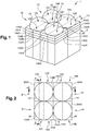
- the figure 1 is an exploded perspective view, schematic and partial, of an embodiment of an image sensor 1.
- This image sensor 1 comprises a matrix of coplanar pixels. To simplify, only four pixels 10, 12, 14 and 16 of the image sensor 1 have been represented in figure 1 it being understood that, in practice, the image sensor 1 may have more pixels.
- the image sensor 1 comprises, for example, several million or even several tens of millions of pixels.
- the pixels 10, 12, 14 and 16 are located on the surface of a CMOS support 3, for example a piece of silicon wafer on and inside which integrated circuits (not shown) have been. made in CMOS technology (Complementary Metal Oxide Semiconductor). These integrated circuits form, in this example, a matrix of reading circuits associated with the pixels 10, 12, 14 and 16 of the image sensor 1.
- a reading circuit. reading is understood to mean a set of read, addressing and control transistors associated with each pixel.
- photodetectors 10A, 10B, 12A, 12B, 14A, 14B, 16A and 16B can correspond to organic photodiodes (Organic Photodiode - OPD) or to organic photoresistors. In the remainder of the description, it is considered that the photodetectors of the pixels of the image sensor 1 correspond to organic photodiodes.
- first electrodes will also be designated by the expression “lower electrodes” while the second electrodes will also be designated by the expression “upper electrodes”.
- each organic photodetector constitutes an anode electrode while the lower electrode of each organic photodetector constitutes a cathode electrode.
- each pixel has a lens 18, also called a microlens 18 because of its dimensions.
- the pixels 10, 12, 14 and 16 each comprise a lens 18.
- Each lens 18 thus covers all or part of the first and second photodetectors of each pixel of the image sensor 1. More precisely, the lens 18 covers physically the upper electrodes of the first and second photodetectors of the pixel.
- the figure 2 is a top view, schematic and partial, of the image sensor 1 of the figure 1 .
- the lenses 18 completely cover the respective electrodes of the pixels with which they are associated.
- the pixels are substantially square, preferably square. All the pixels of the image sensor 1 preferably have identical dimensions, except for manufacturing dispersions.
- the square formed by each pixel of the image sensor 1, seen from above in figure 2 has a side between approximately 0.8 ⁇ m and 10 ⁇ m, preferably between approximately 0.8 ⁇ m and 3 ⁇ m, even more preferably between 0.8 ⁇ m and 3 ⁇ m.
- the first photodetector and the second photodetector belonging to the same pixel are both rectangular in shape. These photodetectors have substantially the same dimensions and are part of the square formed by the pixel to which they belong.
- each photodetector of each pixel of the image sensor 1 has a length substantially equal to the side of the square formed by each pixel and a width substantially equal to half of the side of the square formed by each pixel. A space is however left between the first and the second photodetector of each pixel, so that their respective lower electrodes are separate.
- each microlens 18 present viewed from above in figure 2 , a diameter substantially equal, preferably equal, to the side of the square formed by the pixel to which it belongs.
- each pixel comprises a microlens 18.
- Each microlens 18 of the image sensor 1 is preferably centered with respect to the square formed by the photodetectors that it covers.
- each microlens 18 may be replaced with another type of micrometric-sized optical element, such as a micrometer-sized Fresnel lens, a micrometer-sized gradient index lens, or a micrometer-sized diffraction grating.
- the microlenses 18 are convergent lenses each having a focal length f of between 1 ⁇ m and 100 ⁇ m, preferably between 1 ⁇ m and 10 ⁇ m. According to one embodiment, all of the microlenses 18 are substantially identical.
- the microlenses 18 can be made of silica, polymethyl methacrylate (PMMA), a positive photosensitive resin, polyethylene terephthalate (PET), polyethylene naphthalate (PEN), cycloolefin copolymer (COP), polydimethylsiloxane (PDMS ) / silicone, or epoxy resin.
- PMMA polymethyl methacrylate
- PET polyethylene terephthalate
- PEN polyethylene naphthalate
- COP cycloolefin copolymer
- PDMS polydimethylsiloxane
- silicone resin epoxy resin.
- the microlenses 18 can be formed by creeping blocks of a photosensitive resin.
- the microlenses 18 can further be formed by molding on a layer of PET, PEN, COP, PDMS / silicone or epoxy resin.
- the figure 3 is an electrical diagram of an embodiment of circuits for reading two pixels of the image sensor of the figures 1 and 2 .
- the first read circuit 20A of the first photodetector 10A of pixel 10 and the second read circuit 20B of the second photodetector 10B of pixel 10 jointly form a read circuit 20 of pixel 10.
- first photodetector 12A of pixel 12 and the second circuit reading 22B of the second photodetector 12B of pixel 12 jointly form a reading circuit 22 of pixel 12.
- each read circuit 20A, 20B, 22A, 22B comprises three MOS transistors. Such a circuit is commonly designated, with its photodetector, by the expression “3T sensor”.
- each read circuit 20A, 22A associated with a first photodetector comprises a MOS transistor in follower assembly 200, in series with a selection MOS transistor 202, between two terminals 204 and 206A.
- each read circuit 20B, 22B associated with a second photodetector comprises a MOS transistor in follower assembly 200, in series with a selection MOS transistor 202, between two terminals 204 and 206B.
- Each terminal 204 is connected to a source of a high reference potential, denoted Vpix, in the case where the transistors of the read circuits are N-channel MOS transistors.
- Each terminal 204 is connected to a source of a potential of low reference, for example ground, in the case where the transistors of the read circuits are P-channel MOS transistors.
- Each terminal 206A is connected to a first conductive track 208A.
- the first conductive track 208A can be connected to all the first photodetectors of the same column.
- the first conductive track 208A is preferably connected to all the first photodetectors of the image sensor 1.
- each terminal 206B is connected to a second conductive track 208B.
- the second conductive track 208B can be connected to all the second photodetectors of the same column.
- the second conductive track 208B is preferably connected to all second photodetectors of the image sensor 1.
- the second conductive track 208B is preferably separate from the first conductive track 208A.
- the first conductive track 208A is connected to a first current source 209A which is not part of the read circuits 20, 22 of the pixels 10, 12 of the image sensor 1.
- the second conductive track 208B is connected to a second current source 209B which is not part of the read circuits 20, 22 of the pixels 10, 12 of the image sensor 1.
- the current sources 209A and 209B of the image sensor 1 are external to the pixels and reading circuits.
- the gate of transistor 202 is intended to receive a signal, denoted SEL_R1, for selection of pixel 10 in the case of read circuit 20 of pixel 10.
- the gate of transistor 202 is intended to receive another signal, denoted SEL_R2, for selection. of pixel 12 in the case of read circuit 22 of pixel 12.
- Each node FD_1A, FD_1B, FD_2A, FD_2B is connected, by a reset MOS transistor 210, to a terminal of application of a reset potential Vrst, this potential possibly being identical to the potential Vpix.
- the gate of transistor 210 is intended to receive an RST signal of photodetector reset command, making it possible in particular to reset the node FD_1A, FD_1B, FD_2A or FD_2B substantially to the potential Vrst.
- the potential Vtop_C1 is applied to the first upper electrode common to all the first photodetectors.
- the potential Vtop_C2 is, for its part, applied to the second upper electrode common to all the second photodetectors.
- VSEL_R1 the application of the voltage VSEL_R1, respectively VSEL_R2, is controlled by the binary signal denoted SEL_R1, respectively SEL_R2.
- the figure 4 is a timing diagram of signals of an example of operation of the image sensor 1 having the reading circuits of the figure 3 .
- the chronogram of the figure 4 corresponds, more particularly, to an example of operation of the image sensor 1 in “time of flight” mode (Time of Flight - ToF).
- time of flight Time of Flight - ToF
- the pixels of the image sensor 1 are used to evaluate a distance separating them from a subject (object, scene, face, etc.) placed or located opposite this image sensor.
- To evaluate this distance we start by emitting a light pulse in the direction of the subject with an associated emitting system not described in this text. This light pulse is usually obtained by briefly illuminating the subject with radiation from a source, for example near infrared radiation from a light emitting diode. This light pulse is then at least partially reflected by the subject, then picked up by the image sensor 1.
- a time taken by the light pulse to travel back and forth between the source and the subject is then calculated or measured.
- the image sensor 1 being advantageously located close to the source, this duration corresponds approximately to double the time taken by the light pulse to travel the distance separating the subject from this image sensor 1.
- the chronogram of the figure 4 illustrates an example of the evolution of the binary signals RST and SEL_R1 as well as of the potentials Vtop_C1, Vtop_C2, VFD_1A and VFD_1B of two photodetectors of the same pixel of the image sensor 1, for example the first photodetector 10A and the second photodetector 10B of the pixel 10.
- the figure 4 also represents, in dotted lines, the binary signal SEL_R2 of another pixel of the image sensor 1, for example the pixel 12.
- the timing diagram of the figure 4 was established by considering that the MOS transistors of the read circuit 20 of the pixel 10 are N-channel transistors.
- the signal SEL_R1 is in the low state so that the transistors 202 of the pixel 10 are turned off.
- a reset phase is then initiated.
- the RST signal is kept high so that the reset transistors 210 of pixel 10 are on.
- the charges accumulated in the photodiodes 10A and 10B are then evacuated to the source of the potential Vrst.
- the potential Vtop_C1 is, always at time t0, at a high level.
- This high level corresponds to a bias of the first photodetector 10A under a voltage greater than a voltage resulting from the application of a potential called “intrinsic potential” (built-in potential).
- This potential intrinsic is equivalent to a difference between an anode output work and a cathode output work.
- the potential Vtop_C1 is put at a low level.
- This low level corresponds to a bias of the first photodetector 10A under a negative voltage, that is to say less than 0 V. This thus allows the first photodetector 10A to integrate photogenerated charges.
- What has been described previously in relation to the polarization of the first photodetector 10A by the potential Vtop_C1 is transposed to the explanation of the operation of the polarization of the second photodetector 10B by the potential Vtop_C2.
- a first infrared light pulse (IR light emitted) towards a scene comprising one or more objects from which it is desired to measure the distance, which makes it possible to acquire a depth map of the scene.
- This first infrared light pulse has a duration denoted tON.
- the RST signal is set low, so that the reset transistors 210 of pixel 10 are turned off, and the potential Vtop_C2 is set high.
- the potential Vtop_C1 being at the low level, one thus begins, at the instant t1, a first phase of integration, denoted ITA, in the first photodetector 10A of the pixel 10 of the image sensor 1.
- integration phase denotes of a pixel the phase during which the pixel collects charges under the effect of incident radiation.
- tD a second infrared light pulse (IR light received) resulting from the reflection of the first pulse infrared light by an object in the scene, or by a point of an object, the distance of which is to be measured from pixel 10.
- the duration tD is therefore a function of the distance of the object from the sensor 1.
- CCA a first charge collection phase, denoted CCA, in the first photodetector 10A.
- This first charge collection phase corresponds to a period during which charges are generated in proportion to the intensity of the incident light, that is to say in proportion to the light intensity of the second pulse, in the photodetector 10A.
- the first phase of charge collection causes a drop in the level of the potential VFD_1A at the node FD_1A of the read circuit 20A.
- the first infrared light pulse ceases to be emitted.
- the potential Vtop_C1 is simultaneously put at the high level, thus marking the end of the first phase of integration, therefore of the first phase of collection of charges.
- a second integration phase is started, denoted ITB, in the second photodetector 10B of pixel 10 of image sensor 1. Since second photodetector 10B receives light from the second light pulse, a second charge collection phase, denoted CCB, is started, still at the instant t3.
- the second phase of charge collection causes a drop in the level of the potential VFD_1B at the node FD_1B of the read circuit 20B.
- the second light pulse ceases to be picked up by the second photodetector 10B of pixel 10.
- the second charge collection phase therefore ends at this instant t4.
- the potential Vtop_C2 is set to the high level. This marks the end of the second phase of integration.
- a reading phase is carried out, denoted RT, during which a measurement of the quantity of charges collected by the photodiodes of the pixels of the image sensor 1 is carried out .
- RT a reading phase
- the rows of pixels of the image sensor 1 are read sequentially.
- the signals SEL_R1 and SEL_R2 are successively set to the high state to alternately read the pixels 10 and 12 of the image sensor 1.
- a new reset phase (RESET) is started.
- the RST signal is set high so that the reset transistors 210 of pixel 10 are on.
- the charges accumulated in the photodiodes 10A and 10B are then evacuated to the source of the potential Vrst.
- the magnitude noted AVFD_1A corresponds to a drop in potential VFD_1A during the integration phase of the first photodetector 10A.
- the magnitude noted AVFD_1B corresponds to a drop in potential VFD_1B during the integration phase of the second photodetector 10B.
- a new distance evaluation is started by the emission of a second light pulse.
- This new distance evaluation includes times t2 'and t4' similar to times t2 and t4, respectively.
- the operation of the image sensor 1 has been illustrated above in relation to an example of operation in time-of-flight mode, in which the photodetectors of one and the same pixel are controlled in a desynchronized manner.
- An advantage of the image sensor 1 is that it can also operate in other modes, in particular modes in which the photodetectors of the same pixel are controlled in a synchronized manner.
- the image sensor 1 can, for example, be driven in global shutter mode, that is to say that this image sensor 1 can also implement an image acquisition method in in which the beginnings and ends of the pixel integration phases are simultaneous.
- An advantage of the image sensor 1 is therefore to be able to operate alternately according to different modes.
- the image sensor 1 can, for example, operate alternately in time-of-flight mode and in global shutter imaging mode.
- the image sensor 1 can thus be used to take different types of images without loss of resolution, because the different imaging modes that can be implemented by this image sensor 1 use the same number of pixels.
- the figures 5 to 13 below illustrate successive steps of an embodiment of a method for producing the image sensor 1 of the figures 1 and 2 .
- a method for producing the image sensor 1 of the figures 1 and 2 To simplify, what is explained below in relation to the figures 5 to 13 illustrates the production of a single pixel of the image sensor 1, for example the pixel 12 of the image sensor 1.
- this method can be extended to the production of any number of pixels of an image sensor similar to image sensor 1.
- the figure 5 is a sectional view, schematic and partial, of a step of an embodiment of a method for producing the image sensor 1 of the figures 1 and 2 .
- the contact recovery elements 32A and 32B are for example produced from conductive tracks formed on the upper surface 30 of the CMOS support 3 (horizontal parts of the contact recovery elements 32A and 32B) and from conductive vias (vertical parts of the contact elements. contact recovery 32A and 32B) contacting these conductive tracks.
- the conductive tracks and the conductive vias can be made of a metallic material, for example silver (Ag), aluminum (Al), gold (Au), copper (Cu), nickel (Ni), titanium (Ti) and chromium (Cr), or titanium nitride (TiN).
- the conductive tracks and the conductive vias can have a monolayer or multilayer structure.
- these conductive tracks may consist of a stack of conductive layers separated by insulating layers. The vias then pass through these insulating layers.
- the conductive layers may be of a metallic material from the above list and the insulating layers may be of silicon nitride (SiN) or of silicon oxide (SiO 2 ).
- the CMOS support 3 is cleaned in order to remove any impurities found on its surface 30.
- This cleaning is carried out, for example, by plasma. The cleaning thus makes it possible to obtain satisfactory cleanliness of the CMOS support 3 before carrying out a series of successive deposits, detailed in relation to the figures below.
- the mode of implementation of the method described in relation to the figures 6 to 13 consists exclusively of performing operations above the upper surface 30 of the CMOS holder 3.
- the CMOS holder 3 of the figures 6 to 13 is therefore preferably identical to the CMOS support 3 as explained in relation to the figure 5 during the whole process. To simplify, the CMOS 3 support will therefore not be detailed again in the figures below.
- the figure 6 is a sectional view, schematic and partial, of another step of the mode of implementation of the method for producing the image sensor 1 of the figures 1 and 2 from the structure as described in relation to the figure 5 .
- one proceeds to a full plate deposition of an electron injector material having a sufficiently low lateral conductivity so as not to create conduction paths between two neighboring contact recovery elements.
- the lower electrodes 122A and 122B constitute electron injection layers (Electron Injection Layer - EIL) of photodetectors 12A and 12B, respectively. These lower electrodes 122A and 122B are also called cathodes of photodetectors 12A and 12B.
- the lower electrodes 122A and 122B are preferably produced by spin coating or by dip coating.
- the lower electrodes 122A and 122B can have a single or multi-layered structure.
- the figure 7 is a sectional view, schematic and partial, of yet another step of the mode of implementation of the method for making the image sensor 1 of the figures 1 and 2 from the structure as described in relation to the figure 6 .
- a non-selective deposition of a first layer 120 on the side of the upper surface 30 of the CMOS support 3 is carried out.
- This deposition is qualified as a “full plate” deposition because it covers the entire upper surface. 30 of the CMOS support 3 as well as the free surfaces of the contact recovery elements 32A, 32B and of the lower electrodes 122A and 122B.
- the deposition of the first layer 120 is preferably carried out by centrifugal spin coating.
- the first layer 120 is intended to form the future active layers 120A and 120B of the photodetectors 12A and 12B of the pixel 12.
- the active layers 120A and 120B of the photodetectors 12A and 12B of the pixel 12 preferably have , a composition and a thickness identical to those of the first layer 120.
- the first layer 120 can include small molecules, oligomers or polymers. They may be organic or inorganic materials, in particular comprising quantum dots.
- the first layer 120 may comprise an ambipolar semiconductor material, or a mixture of an N-type semiconductor material and a P-type semiconductor material, for example in the form of superimposed layers or of an intimate mixture at the nanoscale. so as to form a heterojunction in volume.
- the thickness of the first layer 120 may be between 50 nm and 2 ⁇ m, for example of the order of 300 nm.
- N-type semiconductor materials suitable for making the layer 120 are fullerenes, in particular C60, [6,6] -phenyl-C 61 -butanoate ([60] PCBM), [6, 6] -phenyl-C 71 -butanoate of methyl ([70] PCBM), perylene diimide, zinc oxide (ZnO) or nanocrystals allowing the formation of quantum dots (quantum dots).
- the figure 8 is a sectional view, schematic and partial, of yet another step of the mode of implementation of the method for making the image sensor 1 of the figures 1 and 2 from the structure as described in relation to the figure 7 .
- a non-selective deposition of a second layer 124 is carried out on the side of the upper surface 30 of the CMOS support 3.
- This deposition is qualified as a “full plate” deposition because it covers the entire upper surface. of the first layer 120.
- the deposition of the second layer 124 is preferably carried out by centrifugal spin coating.
- the second layer 124 is intended to form the future upper electrodes 124A and 124B of the photodetectors 12A and 12B of the pixel 12.
- the upper electrodes 124A and 124B of the photodetectors 12A and 12B of the pixel 12 preferably have , a composition and a thickness identical to those of the second layer 124.
- the second layer 124 is at least partially transparent to the light radiation that it receives.
- the second layer 124 may be of a conductive and transparent material, for example of conductive and transparent oxide (Transparent Conductive Oxide - TCO), of carbon nanotubes, of graphene, of a conductive polymer, of a metal, or of a mixture or an alloy of at least two of these compounds.
- the second layer 124 can have a single-layer or a multi-layer structure.
- TCO suitable for producing the second layer 124 examples include indium-tin oxide (Indium Tin Oxide - ITO), aluminum-zinc oxide (Aluminum Zinc Oxide - AZO), gallium-zinc (Gallium Zinc Oxide - GZO), titanium nitride (TiN), molybdenum oxide (MoO 3 ) and tungsten oxide (WO 3 ).
- An example of a conductive polymer suitable for making the second layer 124 is the polymer known under the name PEDOT: PSS, which is a mixture of poly (3,4) -ethylenedioxythiophene and of sodium polystyrene sulfonate and polyaniline, also called PAni.
- Examples of metals suitable for making the second layer 124 are silver, aluminum, gold, copper, nickel, titanium and chromium.
- An example of a multilayer structure suitable for making the second layer 124 is a multilayer structure of AZO and silver of the AZO / Ag / AZO type.
- the thickness of the second layer 124 may be between 10 nm and 5 ⁇ m, for example of the order of 30 nm. In the case where the second layer 124 is metallic, the thickness of this second layer 124 is less than or equal to 20 nm, preferably less than or equal to 10 nm.
- the figure 9 is a sectional view, schematic and partial, of yet another step of the mode of implementation of the method for producing the image sensor of figures 1 and 2 from the structure as described in relation to the figure 8 .
- three vertical openings 340, 342 and 344 are made through the first layer 120 and the second layer 124 up to the upper surface 30 of the CMOS support 3. These openings are preferably made by etching afterwards.
- masking of the areas to be protected for example by deposition of photosensitive resin, exposure through a mask then dry etching, for example by reactive ionic etching, or by wet etching, for example by chemical etching.
- the deposition of the etching mask is carried out in a localized manner, for example by screen printing, by heliography, by nano-printing (nano imprint) or by flexography, and the etching is carried out by dry etching, for example by reactive ionic etching. , or by wet etching, for example by chemical etching.
- These vertical openings 340, 342 and 344 are to separate photodetectors belonging to the same line of the image sensor 1.
- the openings 340, 342 and 344 are, for example, produced by photolithography.
- the openings 340, 342 and 344 are produced by reactive ionic etching or by chemical etching using a suitable solvent.
- the upper electrodes 124A and 124B constitute Hole Injection Layer (HIL) layers of the photodetectors 12A and 12B, respectively. These upper electrodes 124A and 124B are also called anodes of the photodetectors 12A and 12B.
- HIL Hole Injection Layer
- the upper electrodes 124A and 124B are preferably made of the same material as the layer 124 in which they are formed, as discussed in connection with figure 8 .
- the figure 10 is a sectional view, schematic and partial, of yet another step of the mode of implementation of the method for making the image sensor 1 of the figures 1 and 2 from the structure as described in relation to the figure 9 .
- the openings 340, 342 and 344 are filled in with a third insulation layer 35 of which only parts 350, 352 and 354 are visible in figure 10 .
- the parts 350, 352 and 354 of the third insulation layer 35 respectively fill the openings 340, 342 and 344.
- the purpose of the parts 350, 352 and 354 of the third layer 35 is to electrically isolate neighboring photodetectors belonging to the same line of the image sensor 1.
- the parts 350, 352 and 354 of the third layer 35 at least partially absorb the light received by the image sensor 1 in order to optically isolate the photodetectors of the same line.
- the third insulating layer can be made from a resin whose absorption covers at least the wavelengths of the photodiodes (visible and infrared). Such a resin, with a black appearance, is then qualified as “black resin”.
- part 352 electrically and optically isolates the first photodetector 12A from the second photodetector 12B of pixel 12.
- the third insulating layer 35 may be made of an inorganic material, for example of silicon oxide (SiO 2 ) or of silicon nitride (SiN).
- this material is preferably obtained by physical vapor deposition (Physical Vapor Deposition - PVD) or by plasma-enhanced chemical vapor deposition (Plasma-Enhanced). Chemical Vapor Deposition - PECVD).
- the third insulating layer 35 can be made of fluoropolymer, in particular the fluoropolymer known under the trade name “Cytop” from the company Bellex, of polyvinylpyrrolidone (PVP), of polymethyl methacrylate (PMMA), of polystyrene (PS), of parylene, polyimide (PI), acrylonitrile butadiene styrene (ABS), polydimethylsiloxane (PDMS), a photolithography resin, epoxy resin, acrylate resin or a mixture of at least two of these compounds.
- PVP polyvinylpyrrolidone
- PMMA polymethyl methacrylate
- PS polystyrene
- PS polystyrene
- parylene polyimide
- PI acrylonitrile butadiene styrene
- ABS acrylonitrile butadiene styrene
- PDMS polydimethylsiloxane
- the third insulating layer 35 may be made from another inorganic dielectric, in particular from aluminum oxide (Al 2 O 3 ).
- Aluminum oxide can be deposited by depositing thin atomic layers (Atomic Layer Deposition - ALD).
- the maximum thickness of the third insulating layer 35 may be between 50 nm and 2 ⁇ m, for example of the order of 100 nm.
- a fourth layer 360 is then deposited over the entire structure on the side of the upper surface 30 of the CMOS support 3.
- This fourth layer 360 is preferably a so-called “planarization” layer making it possible to obtain a structure having a flat upper surface. before encapsulation of the photodetectors.
- the fourth planarization layer 360 may be made of a dielectric material based on polymers.
- the planarization layer 360 can alternatively contain a mixture of silicon nitride (SiN) and silicon oxide (SiO 2 ), this mixture being obtained by sputtering, by physical vapor deposition (PVD). ) or by plasma-enhanced chemical vapor deposition (PECVD).
- the planarization layer 360 can also be made of fluoropolymer, in particular the fluoropolymer known under the trade name “Cytop” from the company Bellex, of polyvinylpyrrolidone (PVP), of polymethyl methacrylate (PMMA), of polystyrene (PS), made of parylene, polyimide (PI), acrylonitrile butadiene styrene (ABS), polydimethylsiloxane (PDMS), a photolithography resin, epoxy resin, acrylate resin or a mixture of at least two of these compounds.
- PVP polyvinylpyrrolidone
- PMMA polymethyl methacrylate
- PS polystyrene
- PS polystyrene
- PI polyimide
- ABS acrylonitrile butadiene styrene
- PDMS polydimethylsiloxane
- the figure 11 is a sectional view, schematic and partial, of a variant of the embodiment of the method for producing the image sensor 1 of the figures 1 and 2 from the structure as described in relation to the figure 9 .
- This variant differs from the step explained in relation to the figure 10 mainly in that the openings 340, 342 and 344 are here not respectively filled (or filled in) by the parts 350, 352 and 354 of the third insulation layer 35 but by a layer 360 'consisting, preferably, of a material identical to that of the fourth layer 360.
- the variant illustrated in figure 11 amounts to not carrying out the deposition of the third insulation layer 35 and to proceeding directly to the deposition of the fourth layer 360 to form the fifth layer 360 ′.
- the fifth layer 360 ′ is not made of black resin.
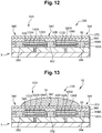
- the figure 12 is a sectional view, schematic and partial, of yet another step of the mode of implementation of the method for making the image sensor 1 of the figures 1 and 2 from the structure as described in relation to the figure 10 .
- a sixth layer 370 is deposited over the entire structure on the side of the upper surface 30 of the CMOS support 3.
- the purpose of this sixth layer 370 is to encapsulate the organic photodetectors of the image sensor 1.
- the sixth layer 370 thus makes it possible to avoid the degradation, due to exposure to water or to humidity contained in the ambient air, of the organic materials constituting the photodetectors of the image sensor 1.
- the sixth layer 370 covers the entire free upper surface of the fourth planarization layer 360.
- the sixth layer 370 may consist of alumina (Al 2 O 3 ) obtained by a deposition process by thin atomic layers (Atomic Layer Deposition - ALD), of silicon nitride (Si 3 N 4 ) or of silicon oxide. (SiO 2 ) obtained by physical vapor deposition (PVD) of silicon nitride obtained by plasma assisted chemical vapor deposition (PECVD).
- the sixth layer 370 may alternatively consist of PET, PEN, COP or CPI.
- the sixth layer 370 makes it possible to further improve the surface condition of the structure before making the microlenses.
- the figure 13 is a sectional view, schematic and partial, of yet another step of the mode of implementation of the method for making the image sensor 1 of the figures 1 and 2 from the structure as described in relation to the figure 12 .
- the microlens 18 of the pixel 12 is produced directly above the photodetectors 12A and 12B.
- this microlens 18 is substantially centered relative to the opening 342 separating the two photodetectors 12A, 12B.
- the microlens 18 is approximately aligned with respect to the portion 352 of the third insulation layer 35 ( figure 10 ). We thus obtain pixel 12 of image sensor 1.
- the process for forming the layers of the image sensor 1 may correspond to a so-called additive process, for example by direct printing of the material composing the organic layers at the desired locations, in particular in the form of sol-gel, for example by inkjet printing, heliography, screen printing, flexography, spray coating or drop-casting.
- the process for forming the layers of the image sensor may correspond to a so-called subtractive process, in which the material composing the organic layers is deposited on the entire structure and in which the portions unused are then removed, for example by photolithography or laser ablation.
- the deposition on the entire structure can be carried out for example by liquid, by cathodic sputtering or by evaporation. They may in particular be processes of the spin coating, spray coating, heliography, slot-die coating, blade coating, flexography or screen printing type.
- the layers are metallic, the metal is, for example, deposited by evaporation or by cathodic sputtering on the whole of the support and the metallic layers are delimited by etching.
- the layers of the image sensor can be produced by printing techniques.
- the materials of these layers described above can be deposited in liquid form, for example in the form of conductive and semiconductor inks using inkjet printers.
- the term “materials in liquid form” is understood here also to mean gel materials which can be deposited by printing techniques.
- Annealing steps are optionally provided between the depositions of the different layers, but the annealing temperatures may not exceed 150 ° C., and the deposition and any annealing may be carried out at atmospheric pressure.
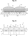
- the figure 14 is a sectional view along plane AA ( figure 2 ), schematic and partial, of the image sensor 1 of the figures 1 and 2 .
- the cutting plane AA corresponds to a cutting plane parallel to a line of pixels of the image sensor 1.
- the figure 15 is a sectional view along plane BB ( figure 2 ), schematic and partial, of the image sensor 1 of the figures 1 and 2 .
- the cutting plane BB corresponds to a cutting plane parallel to a column of pixels of the image sensor 1.
- all the first photodetectors of the pixels belonging to a same column of pixels of the image sensor 1 have a common active layer and a common upper electrode.
- the upper electrode thus makes it possible to address all the first photodetectors of the pixels of a same column, while the lower electrode makes it possible to address each first photodetector individually.
- all the second photodetectors of the pixels belonging to a same column of pixels of the image sensor 1 have another common active layer, distinct from the common active layer of the first photodetectors of these same pixels, and another common upper electrode, distinct from the common upper electrode of the first photodetectors of these same pixels.
- This other common upper electrode thus makes it possible to address all the second photodetectors of the pixels of a same column, while the lower electrode makes it possible to address each second photodetector individually.
- the figure 16 is a sectional view, schematic and partial, of another embodiment of an image sensor 4.
- the color filters 41R, 41G and 41B of the image sensor 4 allow electromagnetic waves to pass in different frequency ranges of the visible spectrum and allow electromagnetic waves of the infrared spectrum to pass.
- 41R, 41G and 41B color filters can match colored resin blocks.
- Each color filter 41R, 41G and 41B is adapted to pass infrared radiation, for example at a wavelength between 700 nm and 1 mm, and, for at least some of the color filters, to pass a range of lengths visible light wave.
- the photodetectors of each pixel 10, 12, 14 and 16 are coplanar and each associated with a read circuit as discussed in relation to the figure 3 . These read circuits are produced on and inside the CMOS support 3.
- the image sensor 4 is thus capable, for example, of alternately carrying out estimates of distance by time of flight in the infrared and captures of images. color images.
Applications Claiming Priority (1)
| Application Number | Priority Date | Filing Date | Title |
|---|---|---|---|
| FR1908251A FR3098989B1 (fr) | 2019-07-19 | 2019-07-19 | Pixel de capteur d’images |
Publications (1)
| Publication Number | Publication Date |
|---|---|
| EP3767677A1 true EP3767677A1 (de) | 2021-01-20 |
Family
ID=69172849
Family Applications (2)
| Application Number | Title | Priority Date | Filing Date |
|---|---|---|---|
| EP20739697.9A Pending EP4000096A1 (de) | 2019-07-19 | 2020-07-16 | Bildsensorpixel |
| EP20186097.0A Pending EP3767677A1 (de) | 2019-07-19 | 2020-07-16 | Pixel eines bildsensors |
Family Applications Before (1)
| Application Number | Title | Priority Date | Filing Date |
|---|---|---|---|
| EP20739697.9A Pending EP4000096A1 (de) | 2019-07-19 | 2020-07-16 | Bildsensorpixel |
Country Status (8)
| Country | Link |
|---|---|
| US (1) | US20220262863A1 (de) |
| EP (2) | EP4000096A1 (de) |
| JP (1) | JP2022541305A (de) |
| KR (1) | KR20220032096A (de) |
| CN (2) | CN114270521A (de) |
| FR (1) | FR3098989B1 (de) |
| TW (1) | TW202118031A (de) |
| WO (1) | WO2021013666A1 (de) |
Families Citing this family (1)
| Publication number | Priority date | Publication date | Assignee | Title |
|---|---|---|---|---|
| KR20210013508A (ko) * | 2019-07-26 | 2021-02-04 | 삼성디스플레이 주식회사 | 광 센서, 광 센서의 제조 방법 및 광 센서를 포함하는 표시 장치 |
Citations (6)
| Publication number | Priority date | Publication date | Assignee | Title |
|---|---|---|---|---|
| US20130182173A1 (en) | 2012-01-13 | 2013-07-18 | Nikon Corporation | Solid-state imaging device and electronic camera |
| US20160105622A1 (en) | 2014-10-08 | 2016-04-14 | Panasonic Intellectual Property Management Co., Ltd. | Imaging device |
| DE102016102111A1 (de) | 2015-02-16 | 2016-08-18 | Samsung Electronics Co., Ltd. | Bildsensor und bildgebende Vorrichtung mit demselben |
| EP3209012A1 (de) | 2016-02-19 | 2017-08-23 | Samsung Electronics Co., Ltd | Elektronische vorrichtung und betriebsverfahren damit |
| US20170257587A1 (en) | 2014-09-10 | 2017-09-07 | Sony Semiconductor Solutions Corporation | Solid-state imaging device, method for driving the same, and electronic device |
| EP3579021A1 (de) * | 2017-02-06 | 2019-12-11 | Panasonic Intellectual Property Management Co., Ltd. | Dreidimensionale bewegungserfassungsvorrichtung und dreidimensionales bewegungserfassungsverfahren |
-
2019
- 2019-07-19 FR FR1908251A patent/FR3098989B1/fr active Active
-
2020
- 2020-07-16 EP EP20739697.9A patent/EP4000096A1/de active Pending
- 2020-07-16 CN CN202080058133.8A patent/CN114270521A/zh active Pending
- 2020-07-16 EP EP20186097.0A patent/EP3767677A1/de active Pending
- 2020-07-16 US US17/627,551 patent/US20220262863A1/en active Pending
- 2020-07-16 WO PCT/EP2020/070072 patent/WO2021013666A1/fr unknown
- 2020-07-16 KR KR1020227004642A patent/KR20220032096A/ko unknown
- 2020-07-16 JP JP2022503875A patent/JP2022541305A/ja active Pending
- 2020-07-17 TW TW109124207A patent/TW202118031A/zh unknown
- 2020-07-20 CN CN202021427741.5U patent/CN213304142U/zh active Active
Patent Citations (6)
| Publication number | Priority date | Publication date | Assignee | Title |
|---|---|---|---|---|
| US20130182173A1 (en) | 2012-01-13 | 2013-07-18 | Nikon Corporation | Solid-state imaging device and electronic camera |
| US20170257587A1 (en) | 2014-09-10 | 2017-09-07 | Sony Semiconductor Solutions Corporation | Solid-state imaging device, method for driving the same, and electronic device |
| US20160105622A1 (en) | 2014-10-08 | 2016-04-14 | Panasonic Intellectual Property Management Co., Ltd. | Imaging device |
| DE102016102111A1 (de) | 2015-02-16 | 2016-08-18 | Samsung Electronics Co., Ltd. | Bildsensor und bildgebende Vorrichtung mit demselben |
| EP3209012A1 (de) | 2016-02-19 | 2017-08-23 | Samsung Electronics Co., Ltd | Elektronische vorrichtung und betriebsverfahren damit |
| EP3579021A1 (de) * | 2017-02-06 | 2019-12-11 | Panasonic Intellectual Property Management Co., Ltd. | Dreidimensionale bewegungserfassungsvorrichtung und dreidimensionales bewegungserfassungsverfahren |
Also Published As
| Publication number | Publication date |
|---|---|
| CN114270521A (zh) | 2022-04-01 |
| EP4000096A1 (de) | 2022-05-25 |
| WO2021013666A1 (fr) | 2021-01-28 |
| KR20220032096A (ko) | 2022-03-15 |
| FR3098989A1 (fr) | 2021-01-22 |
| FR3098989B1 (fr) | 2023-08-25 |
| JP2022541305A (ja) | 2022-09-22 |
| TW202118031A (zh) | 2021-05-01 |
| US20220262863A1 (en) | 2022-08-18 |
| CN213304142U (zh) | 2021-05-28 |
Similar Documents
| Publication | Publication Date | Title |
|---|---|---|
| EP3931872B1 (de) | Farb- und infrarotbildsensor | |
| EP3767679B1 (de) | Pixel eines bildsensors | |
| WO2018162842A1 (fr) | Systeme d'acquisition d'images | |
| WO2020178498A1 (fr) | Capteur d'images couleur et infrarouge | |
| EP3767677A1 (de) | Pixel eines bildsensors | |
| EP4026172A1 (de) | Bildschirmpixel | |
| EP3931873B1 (de) | Farb- und infrarotbildsensor | |
| EP3767678A1 (de) | Pixel eines bildsensors | |
| EP4053900A1 (de) | Hybridsensor | |
| WO2022184409A1 (fr) | Capteur hybride | |
| FR3120472A1 (fr) | Capteur hybride | |
| EP4073842A1 (de) | Bildsensor zum korrigieren des elektronischen rauschens eines sensors | |
| WO2020193889A1 (fr) | Capteur d'images comprenant un filtre angulaire |
Legal Events
| Date | Code | Title | Description |
|---|---|---|---|
| PUAI | Public reference made under article 153(3) epc to a published international application that has entered the european phase |
Free format text: ORIGINAL CODE: 0009012 |
|
| STAA | Information on the status of an ep patent application or granted ep patent |
Free format text: STATUS: THE APPLICATION HAS BEEN PUBLISHED |
|
| AK | Designated contracting states |
Kind code of ref document: A1 Designated state(s): AL AT BE BG CH CY CZ DE DK EE ES FI FR GB GR HR HU IE IS IT LI LT LU LV MC MK MT NL NO PL PT RO RS SE SI SK SM TR |
|
| AX | Request for extension of the european patent |
Extension state: BA ME |
|
| STAA | Information on the status of an ep patent application or granted ep patent |
Free format text: STATUS: REQUEST FOR EXAMINATION WAS MADE |
|
| 17P | Request for examination filed |
Effective date: 20210129 |
|
| RBV | Designated contracting states (corrected) |
Designated state(s): AL AT BE BG CH CY CZ DE DK EE ES FI FR GB GR HR HU IE IS IT LI LT LU LV MC MK MT NL NO PL PT RO RS SE SI SK SM TR |