EP3200178A1 - Pixeltreiberschaltung, verfahren, anzeigetafel und anzeigevorrichtung - Google Patents
Pixeltreiberschaltung, verfahren, anzeigetafel und anzeigevorrichtung Download PDFInfo
- Publication number
- EP3200178A1 EP3200178A1 EP15748154.0A EP15748154A EP3200178A1 EP 3200178 A1 EP3200178 A1 EP 3200178A1 EP 15748154 A EP15748154 A EP 15748154A EP 3200178 A1 EP3200178 A1 EP 3200178A1
- Authority
- EP
- European Patent Office
- Prior art keywords
- driving
- electrode
- transistor
- receive
- control unit
- Prior art date
- Legal status (The legal status is an assumption and is not a legal conclusion. Google has not performed a legal analysis and makes no representation as to the accuracy of the status listed.)
- Granted
Links
- 238000000034 method Methods 0.000 title claims abstract description 23
- 239000003990 capacitor Substances 0.000 claims abstract description 136
- 230000009191 jumping Effects 0.000 claims abstract description 40
- 238000007599 discharging Methods 0.000 claims description 8
- 239000010409 thin film Substances 0.000 claims description 6
- 208000032005 Spinocerebellar ataxia with axonal neuropathy type 2 Diseases 0.000 description 18
- 208000033361 autosomal recessive with axonal neuropathy 2 spinocerebellar ataxia Diseases 0.000 description 18
- 238000004519 manufacturing process Methods 0.000 description 10
- 238000010586 diagram Methods 0.000 description 9
- 230000008569 process Effects 0.000 description 6
- 230000002411 adverse Effects 0.000 description 4
- 230000032683 aging Effects 0.000 description 2
- 229910021417 amorphous silicon Inorganic materials 0.000 description 2
- 230000008859 change Effects 0.000 description 2
- 230000000694 effects Effects 0.000 description 2
- 238000005516 engineering process Methods 0.000 description 2
- 230000007774 longterm Effects 0.000 description 2
- 238000012986 modification Methods 0.000 description 2
- 230000004048 modification Effects 0.000 description 2
- 238000011017 operating method Methods 0.000 description 2
- 229910021420 polycrystalline silicon Inorganic materials 0.000 description 2
- 238000013461 design Methods 0.000 description 1
- 230000005669 field effect Effects 0.000 description 1
- 238000004020 luminiscence type Methods 0.000 description 1
- 239000011159 matrix material Substances 0.000 description 1
- 229920005591 polysilicon Polymers 0.000 description 1
- 238000011160 research Methods 0.000 description 1
- 230000004044 response Effects 0.000 description 1
Images


Classifications
-
- G—PHYSICS
- G09—EDUCATION; CRYPTOGRAPHY; DISPLAY; ADVERTISING; SEALS
- G09G—ARRANGEMENTS OR CIRCUITS FOR CONTROL OF INDICATING DEVICES USING STATIC MEANS TO PRESENT VARIABLE INFORMATION
- G09G3/00—Control arrangements or circuits, of interest only in connection with visual indicators other than cathode-ray tubes
- G09G3/20—Control arrangements or circuits, of interest only in connection with visual indicators other than cathode-ray tubes for presentation of an assembly of a number of characters, e.g. a page, by composing the assembly by combination of individual elements arranged in a matrix no fixed position being assigned to or needed to be assigned to the individual characters or partial characters
- G09G3/22—Control arrangements or circuits, of interest only in connection with visual indicators other than cathode-ray tubes for presentation of an assembly of a number of characters, e.g. a page, by composing the assembly by combination of individual elements arranged in a matrix no fixed position being assigned to or needed to be assigned to the individual characters or partial characters using controlled light sources
- G09G3/30—Control arrangements or circuits, of interest only in connection with visual indicators other than cathode-ray tubes for presentation of an assembly of a number of characters, e.g. a page, by composing the assembly by combination of individual elements arranged in a matrix no fixed position being assigned to or needed to be assigned to the individual characters or partial characters using controlled light sources using electroluminescent panels
- G09G3/32—Control arrangements or circuits, of interest only in connection with visual indicators other than cathode-ray tubes for presentation of an assembly of a number of characters, e.g. a page, by composing the assembly by combination of individual elements arranged in a matrix no fixed position being assigned to or needed to be assigned to the individual characters or partial characters using controlled light sources using electroluminescent panels semiconductive, e.g. using light-emitting diodes [LED]
- G09G3/3208—Control arrangements or circuits, of interest only in connection with visual indicators other than cathode-ray tubes for presentation of an assembly of a number of characters, e.g. a page, by composing the assembly by combination of individual elements arranged in a matrix no fixed position being assigned to or needed to be assigned to the individual characters or partial characters using controlled light sources using electroluminescent panels semiconductive, e.g. using light-emitting diodes [LED] organic, e.g. using organic light-emitting diodes [OLED]
- G09G3/3225—Control arrangements or circuits, of interest only in connection with visual indicators other than cathode-ray tubes for presentation of an assembly of a number of characters, e.g. a page, by composing the assembly by combination of individual elements arranged in a matrix no fixed position being assigned to or needed to be assigned to the individual characters or partial characters using controlled light sources using electroluminescent panels semiconductive, e.g. using light-emitting diodes [LED] organic, e.g. using organic light-emitting diodes [OLED] using an active matrix
- G09G3/3233—Control arrangements or circuits, of interest only in connection with visual indicators other than cathode-ray tubes for presentation of an assembly of a number of characters, e.g. a page, by composing the assembly by combination of individual elements arranged in a matrix no fixed position being assigned to or needed to be assigned to the individual characters or partial characters using controlled light sources using electroluminescent panels semiconductive, e.g. using light-emitting diodes [LED] organic, e.g. using organic light-emitting diodes [OLED] using an active matrix with pixel circuitry controlling the current through the light-emitting element
-
- G—PHYSICS
- G09—EDUCATION; CRYPTOGRAPHY; DISPLAY; ADVERTISING; SEALS
- G09G—ARRANGEMENTS OR CIRCUITS FOR CONTROL OF INDICATING DEVICES USING STATIC MEANS TO PRESENT VARIABLE INFORMATION
- G09G2300/00—Aspects of the constitution of display devices
- G09G2300/04—Structural and physical details of display devices
- G09G2300/0421—Structural details of the set of electrodes
- G09G2300/0426—Layout of electrodes and connections
-
- G—PHYSICS
- G09—EDUCATION; CRYPTOGRAPHY; DISPLAY; ADVERTISING; SEALS
- G09G—ARRANGEMENTS OR CIRCUITS FOR CONTROL OF INDICATING DEVICES USING STATIC MEANS TO PRESENT VARIABLE INFORMATION
- G09G2300/00—Aspects of the constitution of display devices
- G09G2300/04—Structural and physical details of display devices
- G09G2300/0439—Pixel structures
- G09G2300/0465—Improved aperture ratio, e.g. by size reduction of the pixel circuit, e.g. for improving the pixel density or the maximum displayable luminance or brightness
-
- G—PHYSICS
- G09—EDUCATION; CRYPTOGRAPHY; DISPLAY; ADVERTISING; SEALS
- G09G—ARRANGEMENTS OR CIRCUITS FOR CONTROL OF INDICATING DEVICES USING STATIC MEANS TO PRESENT VARIABLE INFORMATION
- G09G2300/00—Aspects of the constitution of display devices
- G09G2300/08—Active matrix structure, i.e. with use of active elements, inclusive of non-linear two terminal elements, in the pixels together with light emitting or modulating elements
- G09G2300/0809—Several active elements per pixel in active matrix panels
- G09G2300/0819—Several active elements per pixel in active matrix panels used for counteracting undesired variations, e.g. feedback or autozeroing
-
- G—PHYSICS
- G09—EDUCATION; CRYPTOGRAPHY; DISPLAY; ADVERTISING; SEALS
- G09G—ARRANGEMENTS OR CIRCUITS FOR CONTROL OF INDICATING DEVICES USING STATIC MEANS TO PRESENT VARIABLE INFORMATION
- G09G2300/00—Aspects of the constitution of display devices
- G09G2300/08—Active matrix structure, i.e. with use of active elements, inclusive of non-linear two terminal elements, in the pixels together with light emitting or modulating elements
- G09G2300/0809—Several active elements per pixel in active matrix panels
- G09G2300/0842—Several active elements per pixel in active matrix panels forming a memory circuit, e.g. a dynamic memory with one capacitor
- G09G2300/0861—Several active elements per pixel in active matrix panels forming a memory circuit, e.g. a dynamic memory with one capacitor with additional control of the display period without amending the charge stored in a pixel memory, e.g. by means of additional select electrodes
-
- G—PHYSICS
- G09—EDUCATION; CRYPTOGRAPHY; DISPLAY; ADVERTISING; SEALS
- G09G—ARRANGEMENTS OR CIRCUITS FOR CONTROL OF INDICATING DEVICES USING STATIC MEANS TO PRESENT VARIABLE INFORMATION
- G09G2310/00—Command of the display device
- G09G2310/02—Addressing, scanning or driving the display screen or processing steps related thereto
- G09G2310/0262—The addressing of the pixel, in a display other than an active matrix LCD, involving the control of two or more scan electrodes or two or more data electrodes, e.g. pixel voltage dependent on signals of two data electrodes
-
- G—PHYSICS
- G09—EDUCATION; CRYPTOGRAPHY; DISPLAY; ADVERTISING; SEALS
- G09G—ARRANGEMENTS OR CIRCUITS FOR CONTROL OF INDICATING DEVICES USING STATIC MEANS TO PRESENT VARIABLE INFORMATION
- G09G2320/00—Control of display operating conditions
- G09G2320/04—Maintaining the quality of display appearance
- G09G2320/043—Preventing or counteracting the effects of ageing
-
- G—PHYSICS
- G09—EDUCATION; CRYPTOGRAPHY; DISPLAY; ADVERTISING; SEALS
- G09G—ARRANGEMENTS OR CIRCUITS FOR CONTROL OF INDICATING DEVICES USING STATIC MEANS TO PRESENT VARIABLE INFORMATION
- G09G2330/00—Aspects of power supply; Aspects of display protection and defect management
- G09G2330/02—Details of power systems and of start or stop of display operation
- G09G2330/028—Generation of voltages supplied to electrode drivers in a matrix display other than LCD
-
- G—PHYSICS
- G09—EDUCATION; CRYPTOGRAPHY; DISPLAY; ADVERTISING; SEALS
- G09G—ARRANGEMENTS OR CIRCUITS FOR CONTROL OF INDICATING DEVICES USING STATIC MEANS TO PRESENT VARIABLE INFORMATION
- G09G3/00—Control arrangements or circuits, of interest only in connection with visual indicators other than cathode-ray tubes
- G09G3/20—Control arrangements or circuits, of interest only in connection with visual indicators other than cathode-ray tubes for presentation of an assembly of a number of characters, e.g. a page, by composing the assembly by combination of individual elements arranged in a matrix no fixed position being assigned to or needed to be assigned to the individual characters or partial characters
- G09G3/22—Control arrangements or circuits, of interest only in connection with visual indicators other than cathode-ray tubes for presentation of an assembly of a number of characters, e.g. a page, by composing the assembly by combination of individual elements arranged in a matrix no fixed position being assigned to or needed to be assigned to the individual characters or partial characters using controlled light sources
- G09G3/30—Control arrangements or circuits, of interest only in connection with visual indicators other than cathode-ray tubes for presentation of an assembly of a number of characters, e.g. a page, by composing the assembly by combination of individual elements arranged in a matrix no fixed position being assigned to or needed to be assigned to the individual characters or partial characters using controlled light sources using electroluminescent panels
- G09G3/32—Control arrangements or circuits, of interest only in connection with visual indicators other than cathode-ray tubes for presentation of an assembly of a number of characters, e.g. a page, by composing the assembly by combination of individual elements arranged in a matrix no fixed position being assigned to or needed to be assigned to the individual characters or partial characters using controlled light sources using electroluminescent panels semiconductive, e.g. using light-emitting diodes [LED]
- G09G3/3208—Control arrangements or circuits, of interest only in connection with visual indicators other than cathode-ray tubes for presentation of an assembly of a number of characters, e.g. a page, by composing the assembly by combination of individual elements arranged in a matrix no fixed position being assigned to or needed to be assigned to the individual characters or partial characters using controlled light sources using electroluminescent panels semiconductive, e.g. using light-emitting diodes [LED] organic, e.g. using organic light-emitting diodes [OLED]
- G09G3/3275—Details of drivers for data electrodes
- G09G3/3291—Details of drivers for data electrodes in which the data driver supplies a variable data voltage for setting the current through, or the voltage across, the light-emitting elements
Definitions
- the present disclosure relates to the field of display technology, in particular to a pixel driving circuit, a pixel driving method, a display panel and a display device.
- An active matrix/organic light-emitting diode (AMOLED) display is one of the current hotspots in the research field of flat-panel displays.
- An organic light-emitting diode (OLED) has such advantages as low power consumption, low production cost, self-luminescence, wide viewing angle and rapid response.
- As a core technology of the AMOLED display the design of a pixel driving circuit is significant and important.
- a stable current is required so as to control the OLED to emit light. Due to the limitations of the manufacture process and the aging of elements, a threshold voltage (Vth) of a driving transistor for each pixel in the AMOELD display will be drifted, which thus results in a change of the current flowing through the OLED of each pixel along with the threshold voltage. As a result, the display brightness is uneven, and thereby an image display effect will be adversely affected.
- Vth threshold voltage
- an existing, basic AMOLED pixel driving circuit merely includes one driving transistor DTFT, one switching transistor T1 and one storage capacitor Cs.
- a scanning voltage Vscan on the scanning line is a low level
- T1 is turned on and a data voltage Vdata is written into the storage capacitor Cs.
- Vscan changes to be a high level
- T1 is turned off
- DTFT is driven by a gate voltage stored in Cs to enable DTFT to generate a current for driving the OLED, thereby to ensure the OLED to emit light continuously within one frame.
- the current I OLED flowing through the OLED is equal to K(V GS -V th ) 2 , where K is a constant, V GS is a gate-source voltage of DTFT, and V th is the threshold voltage of DTFT.
- K is a constant
- V GS is a gate-source voltage of DTFT
- V th is the threshold voltage of DTFT.
- An existing pixel driving circuit having a threshold compensation function may be a 6T1C-based pixel driving circuit, where excessive thin film transistors (TFTs) and lines are used. Though it is able to meet the requirement of threshold compensation, an aperture ratio of the pixel will be reduced correspondingly.
- the existing pixel driving circuit is arranged within each pixel unit, so the OLEDs are distributed in a too compact manner.
- An object of the present disclosure is to provide a pixel driving circuit, a pixel driving method, a display panel and a display device, so as to prevent a small aperture ratio of a pixel due to excessive TFTs and data lines used during the threshold compensation, thereby to improve the image quality and pixels per inch (PPI).
- the present disclosure provides in one embodiment a pixel driving circuit for driving a first light-emitting element and a second light-emitting element. First ends of the first light-emitting element and the second light-emitting element are configured to receive a first level.
- the pixel driving circuit includes a first pixel driving unit and a second pixel driving unit.
- the first pixel driving unit includes a first driving transistor, a first storage capacitor and a first driving control unit.
- a first end of the first storage capacitor is connected to a gate electrode of the first driving transistor, and a second end thereof is configured to receive a data voltage through the first driving control unit.
- the gate electrode of the first driving transistor is connected to a first electrode of the first driving transistor through the first driving control unit, the first electrode thereof is configured to receive a second level through the first driving control unit, and a second electrode thereof is configured to receive the first level through the first driving control unit.
- the second electrode of the first driving transistor is further connected to a second end of the first light-emitting element.
- the first driving control unit is configured to charge and discharge the first storage capacitor through the second level, the data voltage and the first level, so as to apply a jumping voltage onto the data voltage at a first compensation stage, thereby to perform jumping compensation on a threshold voltage of the first driving transistor and control the first light-emitting element to emit light.
- the second pixel driving unit includes a second driving transistor, a second storage capacitor and a second driving control unit.
- a first end of the second storage capacitor is connected to a gate electrode of the second driving transistor, and a second end thereof is configured to receive the data voltage through the first driving control unit.
- the gate electrode of the second driving transistor is connected to a first electrode of the second driving transistor through the second driving control unit, the first electrode thereof is configured to receive the second level through the second driving control unit, and a second electrode thereof is configured to receive the first level through the second driving control unit.
- the second electrode of the second driving transistor is further connected to a second end of the second light-emitting element.
- the second driving control unit is configured to charge and discharge the second storage capacitor through the second level, the data voltage and the first level, so as to apply a jumping voltage onto the data voltage at a second compensation stage, thereby to perform jumping compensation on a threshold voltage of the second driving transistor and control the second light-emitting element to emit light.
- the first driving control unit is of a structure identical to the second driving control unit.
- the first driving control unit includes: a first control transistor, a gate electrode of which is configured to receive a first scanning signal, a, first electrode of which is connected to the first electrode of the first driving transistor, and a second electrode of which is connected to the gate electrode of the first driving transistor; a second control transistor, a gate electrode of which is configured to receive the first scanning signal, a first electrode of which is connected to the second electrode of the first driving transistor, and a second electrode of which is configured to receive the first level; a third control transistor, a gate electrode of which is configured to receive a first driving control signal, a first electrode of which is connected to the second end of the first storage capacitor, and a second electrode of which is configured to receive the data voltage; and a fourth control transistor, a gate electrode of which is configured to receive a second scanning signal, a first electrode of which is configured to receive the second level, and a second electrode of which is connected to the first electrode of the first driving transistor.
- the second driving control unit includes: a fifth control transistor, a gate electrode of which is configured to receive the first scanning signal, a first electrode of which is connected to the first electrode of the second driving transistor, and a second electrode of which is connected to the gate electrode of the second driving transistor; a sixth control transistor, a gate electrode of which is configured to receive the first scanning signal, a first electrode of which is connected to the second electrode of the second driving transistor, and a second electrode of which is configured to receive the first level; a seventh control transistor, a gate electrode of which is configured to receive a second driving control signal, a first electrode of which is connected to the second end of the second storage capacitor, and a second electrode of which is configured to receive the data voltage; and an eighth control transistor, a gate electrode of which is configured to receive the second scanning signal, a first electrode of which is configured to receive the second level, and a second electrode of which is connected to the first electrode of the second driving transistor.
- the first driving transistor, the first control transistor, the second control transistor, the third control transistor and the fourth control transistor are all n-type TFTs
- the second driving transistor, the fifth control transistor, the sixth control transistor, the seventh control transistor and the eighth control transistor are all n-type TFTs.
- the first driving control unit includes: a first control transistor, a gate electrode of which is configured to receive a first scanning signal, a first electrode of which is connected to the first electrode of the first driving transistor, and a second electrode of which is connected to the gate electrode of the first driving transistor; a second control transistor, a gate electrode of which is configured to receive the first scanning signal, a first electrode of which is connected to the second electrode of the first driving transistor, and a second electrode of which is configured to receive the first level; a third control transistor, a gate electrode of which is configured to receive a first driving control signal, a first electrode of which is connected to the second end of the first storage capacitor, and a second electrode of which is configured to receive the data voltage; and a fourth control transistor, a gate electrode of which is configured to receive a second scanning signal, a first electrode of which is configured to receive the second level, and a second electrode of which is connected to the first electrode of the first driving transistor.
- the second driving control unit includes: a fifth control transistor, a gate electrode of which is configured to receive the first scanning signal, a first electrode of which is connected to the first electrode of the second driving transistor, and a second electrode of which is connected to the gate electrode of the second driving transistor; a sixth control transistor, a gate electrode of which is configured to receive the first scanning signal, a first electrode of which is connected to the second electrode of the second driving transistor, and a second electrode of which is configured to receive the first level; a seventh control transistor, a gate electrode of which is configured to receive the second scanning signal, a first electrode of which is connected to the second end of the second storage capacitor, and a second electrode of which is configured to receive the data voltage; and an eighth control transistor, a gate electrode of which is configured to receive the second scanning signal, a first electrode of which is configured to receive the second level, and a second electrode of which is connected to the first electrode of the second driving transistor.
- the first driving transistor, the first control transistor, the second control transistor, the third control transistor and the fourth control transistor are all n-type TFTs; in the second pixel driving unit, the second driving transistor, the fifth control transistor, the sixth control transistor and the eighth control transistor are all n-type TFTs, and the seventh control transistor is a p-type TFT.
- the first driving control unit includes: a first control transistor, a gate electrode of which is configured to receive a first scanning signal, a first electrode of which is connected to the first electrode of the first driving transistor, and a second electrode of which is connected to the gate electrode of the first driving transistor; a second control transistor, a gate electrode of which is configured to receive the first scanning signal, a first electrode of which is connected to the second electrode of the first driving transistor, and a second electrode of which is configured to receive the first level; a third control transistor, a gate electrode of which is configured to receive a first driving control signal, a first electrode of which is connected to the second end of the first storage capacitor, and a second end of which is configured to receive the data voltage; and a fourth control transistor, a gate electrode of which is configured to receive a second driving control signal, a first electrode of which is configured to receive the second level, and a second electrode of which is connected to the first electrode of the first driving transistor.
- the second driving control unit includes: a fifth control transistor, a gate electrode of which is configured to receive the first scanning signal, a first electrode of which is connected to the first electrode of the second driving transistor, and a second electrode of which is connected to the gate electrode of the second driving transistor; a sixth control transistor, a gate electrode of which is configured to receive the first scanning signal, a first electrode of which is connected to the second electrode of the second driving transistor, and a second electrode of which is configured to receive the first level; a seventh control transistor, a gate electrode of which is configured to receive the second driving control signal, a first electrode of which is connected to the second end of the second storage capacitor, and a second electrode of which is configured to receive the data voltage; and an eighth control transistor, a gate electrode of which is configured to receive the second driving control signal, a first electrode of which is configured to receive the second level, and a second electrode of which is connected to the first electrode of the second driving transistor.
- the first driving transistor, the first control transistor, the second control transistor and the third control transistor are all n-type TFTs, and the fourth control transistor is a p-type TFT.
- the second driving transistor, the fifth control transistor, the sixth control transistor and the seventh control transistor are all n-type TFTs, and the eighth control transistor is a p-type TFT.
- the present disclosure provides in one embodiment a pixel driving circuit for driving a first light-emitting element and a second light-emitting element. First ends of the first light-emitting element and the second light-emitting element are configured to receive a first level.
- the pixel driving circuit includes a first pixel driving unit and a second pixel driving unit.
- the first pixel driving unit includes a first driving transistor, a first storage capacitor and a first driving control unit.
- a first end of the first storage capacitor is connected to a gate electrode of the first driving transistor, and a second end thereof is configured to receive a data voltage through the first driving control unit.
- the gate electrode of the first driving transistor is connected to a first electrode of the first driving transistor through the first driving control unit, the first electrode thereof is connected to a second end of the first light-emitting element through the first driving control unit, and a second electrode thereof is configured to receive a second level through the first driving control unit.
- the first driving control unit is configured to reset and charge the first storage capacitor through the second level and the data voltage, so as to apply a jumping voltage onto the data voltage at a first compensation stage, thereby to perform jumping compensation on a threshold voltage of the first driving transistor and control the first driving transistor to drive the first light-emitting element to emit light.
- the second pixel driving unit includes a second driving transistor, a second storage capacitor and a second driving control unit.
- a first end of the second storage capacitor is connected to a gate electrode of the second driving transistor, and a second end thereof is configured to receive the data voltage through the second driving control unit.
- the gate electrode of the second driving transistor is connected to a first electrode of the second driving transistor through the second driving control unit, the first electrode thereof is connected to a second end of the second light-emitting element through the second driving control unit, and a second electrode thereof is configured to receive the second level through the second driving control unit.
- the second driving control unit is configured to reset and charge the second storage capacitor through the second level and the data voltage, so as to apply a jumping voltage onto the data voltage at a second compensation stage, thereby to perform jumping compensation on a threshold voltage of the second driving transistor and control the second driving transistor to drive the second light-emitting element to emit light.
- the first driving control unit is of a structure identical to the second driving control unit.
- the first driving control unit includes: a first control transistor, a gate electrode of which is configured to receive a first driving control signal, a first electrode of which is connected to the first electrode of the first driving transistor, and a second electrode of which is connected to the gate electrode of the first driving transistor; a second control transistor, a gate electrode of which is configured to receive the first driving control signal, a first electrode of which is configured to receive the data voltage, and a second electrode of which is connected to the second end of the first storage capacitor; a third control transistor, a gate electrode of which is configured to receive a first scanning signal, a first electrode of which is connected to the second electrode of the first driving transistor, and a second electrode of which is configured to receive the second level; and a fourth control transistor, a gate electrode of which is configured to receive a second scanning signal, a first electrode of which is connected to the second end of the first light-emitting element, and a second electrode of which is connected to the first electrode of the first driving transistor.
- the second driving control unit includes: a fifth control transistor, a gate electrode of which is configured to receive a second driving control signal, a first electrode of which is connected to the first electrode of the second driving transistor, and a second electrode of which is connected to the gate electrode of the second driving transistor; a sixth control transistor, a gate electrode of which is configured to receive the second driving control signal, a first electrode of which is configured to receive the data voltage, and a second electrode of which is connected to the second end of the second storage capacitor; a seventh control transistor, a gate electrode of which is configured to receive the first scanning signal, a first electrode of which is connected to the second electrode of the second driving transistor, and a second electrode of which is configured to receive the second level; and an eighth control transistor, a gate electrode of which is configured to receive the second scanning signal, a first electrode of which is connected to the second end of the second light-emitting element, and a second electrode of which is connected to the first electrode of the second driving transistor.
- the first driving transistor, the first control transistor, the second control transistor, the third control transistor and the fourth control transistor are all p-type TFTs
- the second driving transistor, the fifth control transistor, the sixth control transistor, the seventh control transistor and the eighth control transistor are all p-type TFTs.
- the present disclosure provides in one embodiment a pixel driving method for driving the above-mentioned pixel driving circuit, including steps of: at a charging stage within one time period, controlling by a first driving control unit a first end of a first storage capacitor to be charged to a second level, and controlling by a second driving control unit a first end of a second storage capacitor to be charged to a second level; at a discharging stage within the time period, controlling by the first driving control unit the first end of the first storage capacitor to be discharged to a threshold voltage of a first driving transistor and controlling a second end of the first storage capacitor to receive a data voltage, and controlling by the second driving control unit the first end of the second storage capacitor to be discharged to a threshold voltage of a second driving transistor and controlling a second end of the second storage capacitor to receive the data voltage, the data voltage being V0 at the discharging stage; at a first compensation stage within the time period, controlling by the first driving control unit the second end of the first storage capacitor to receive the data voltage, and
- the present disclosure provides in one embodiment a pixel driving method for driving the above-mentioned pixel driving circuit, including steps of: at a resetting and charging stage within one time period, controlling by a first driving control unit a first end of a first storage capacitor to be charged to a difference between a second level and a threshold voltage of a first driving transistor and controlling a second end of the first storage capacitor to receive a data voltage, and controlling by a second driving control unit a first end of a second storage capacitor to be charged to a difference between the second level and a threshold voltage of a second driving transistor and controlling a second end of the second storage capacitor to receive the data voltage, the data voltage being ⁇ V1 at the resetting and charging stage; at a first compensation stage within the time period, controlling by the first driving control unit the first end of the first storage capacitor to be in a floating state, thereby compensating for the threshold voltage of the first driving transistor through a gate-source voltage of the first driving transistor, the data voltage being jumped to ⁇ V
- the driving transistors included in the pixel driving circuit are all p-type TFTs, ⁇ V1, ⁇ V2 and ⁇ V3 are greater than 0, ⁇ V3 is greater than ⁇ V2, and ⁇ V2 is greater than ⁇ V1.
- the present disclosure provides in one embodiment a display panel including the above-mentioned pixel driving circuit.
- the present disclosure provides in one embodiment a display device including the above-mentioned display panel.
- two adjacent pixel driving units having a threshold voltage compensation function in the related art are combined so as to share a single data line, thereby it is able to control two pixel units to perform jumping compensation on the threshold voltage of the driving transistor at the corresponding compensation stage through the pixel driving circuit having the threshold voltage compensation function, and to reduce the number of the TFTs desired for the threshold voltage compensation as well as the number of the data lines.
- it is able to remarkably increase an aperture ratio of the pixel unit and reduce the production cost, thereby to improve the image quality and the PPI.
- All transistors adopted in the embodiments of the present disclosure may be thin film transistors (TFTs), field effect transistors (FETs), or any other elements having the same characteristics.
- TFTs thin film transistors
- FETs field effect transistors
- a first electrode may be a source/drain electrode
- a second electrode may be a drain/source electrode.
- the transistor may be an n-type or a p-type transistor
- a driver circuit in the embodiments of the present disclosure may include n-type or p-type transistors.
- the present disclosure provides in a first embodiment a pixel driving circuit for driving a first light-emitting element and a second light-emitting element. First ends of the first light-emitting element and the second light-emitting element are configured to receive a first level.
- the pixel driving circuit includes a first pixel driving unit and a second pixel driving unit.
- the first pixel driving unit includes a first driving transistor, a first storage capacitor and a first driving control unit.
- a first end of the first storage capacitor is connected to a gate electrode of the first driving transistor, and a second end thereof is configured to receive a data voltage through the first driving control unit.
- the gate electrode of the first driving transistor is connected to a first electrode of the first driving transistor through the first driving control unit, the first electrode thereof is configured to receive a second level through the first driving control unit, and a second electrode thereof is configured to receive the first level through the first driving control unit.
- the second electrode of the first driving transistor is further connected to a second end of the first light-emitting element.
- the first driving control unit is configured to charge and discharge the first storage capacitor through the second level, the data voltage and the first level, so as to apply a jumping voltage onto the data voltage at a first compensation stage, thereby to perform jumping compensation on a threshold voltage of the first driving transistor and control the first light-emitting element to emit light.
- the second pixel driving unit includes a second driving transistor, a second storage capacitor and a second driving control unit.
- a first end of the second storage capacitor is connected to a gate electrode of the second driving transistor, and a second end thereof is configured to receive the data voltage through the first driving control unit.
- the gate electrode of the second driving transistor is connected to a first electrode of the second driving transistor through the second driving control unit, the first electrode thereof is configured to receive the second level through the second driving control unit, and a second electrode thereof is configured to receive the first level through the second driving control unit.
- the second electrode of the second driving transistor is further connected to a second end of the second light-emitting element.
- the second driving control unit is configured to charge and discharge the second storage capacitor through the second level, the data voltage and the first level, so as to apply a jumping voltage onto the data voltage at a second compensation stage, thereby to perform jumping compensation on a threshold voltage of the second driving transistor and control the second light-emitting element to emit light.
- two adjacent pixel driving units having a threshold voltage compensation function in the related art are combined so as to share a single data line, thereby it is able to control two pixel units to perform jumping compensation on the threshold voltage of the driving transistor at the corresponding compensation stage through one pixel driving circuit having the threshold voltage compensation function, and to reduce the number of the TFTs desired for the threshold voltage compensation as well as the number of the data lines.
- it is able to remarkably increase an aperture ratio of the pixel unit and reduce the production cost, thereby to improve the image quality and the PPI.
- the light-emitting element may be an organic light-emitting diode (OLED).
- OLED organic light-emitting diode
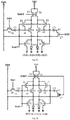
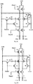
- the present disclosure provides in a second embodiment a pixel driving circuit for driving a first OLED O1 and a second OLED 02.
- Cathodes of the first OLED O1 and the second OLED 02 are both configured to receive a first level V1.
- the pixel driving circuit includes a first pixel driving unit for controlling the first OLED O1 and a second pixel driving unit for controlling the second OLED 02.
- the first driving control unit 21 is configured to charge and discharge the first storage capacitor C1 through the second level V2, the data voltage on the data line Data and the first level V1, so as to control the first driving transistor D1 to drive the first OLED O1 to emit light after compensating for a threshold voltage of the first driving transistor D1 through a gate-source voltage of the first driving transistor D1 at a first compensation stage.
- the second pixel driving unit includes a second driving transistor D2, a second storage capacitor C2 and a second driving control unit 22.
- a first end of the second storage capacitor C2 is connected to a gate electrode of the second driving transistor D2, and a second end thereof is configured to receive the data voltage on the data line Data through the second driving control unit 22.
- the gate electrode of the second driving transistor D2 is connected to a first electrode of the second driving transistor D2 through the second driving control unit 22, the first electrode thereof is configured to receive the second level V2 through the second driving control unit 22, and a second electrode thereof is configured to receive the first level V1 through the second driving control unit 22.
- the second electrode of the second driving transistor D2 is further connected to an anode of the second OLED 02.
- the second driving control unit 22 is configured to charge and discharge the second storage capacitor C2 through the second level V2, the data voltage on the data lien Data and the first level V1, so as to control the second driving transistor D2 to drive the second OLED 02 to emit light after compensating for a threshold voltage of the second driving transistor D2 through a gate-source voltage of the second driving transistor D2 at a second compensation stage.
- D 1 and D2 are both n-type TFTs, and at this time, the first level V1 is a low level, and the second level V2 is a high level.
- the first driving control unit is of a structure identical to the second driving control unit.
- the first driving control unit includes: a first control transistor, a gate electrode of which is configured to receive a first scanning signal, a, first electrode of which is connected to the first electrode of the first driving transistor, and a second electrode of which is connected to the gate electrode of the first driving transistor; a second control transistor, a gate electrode of which is configured to receive the first scanning signal, a first electrode of which is connected to the second electrode of the first driving transistor, and a second electrode of which is configured to receive the first level; a third control transistor, a gate electrode of which is configured to receive a first driving control signal, a first electrode of which is connected to the second end of the first storage capacitor, and a second electrode of which is configured to receive the data voltage; and a fourth control transistor, a gate electrode of which is configured to receive a second scanning signal, a first electrode of which is configured to receive the second level, and a second electrode of which is connected to the first electrode of the first driving transistor.
- the second driving control unit includes: a fifth control transistor, a gate electrode of which is configured to receive the first scanning signal, a first electrode of which is connected to the first electrode of the second driving transistor, and a second electrode of which is connected to the gate electrode of the second driving transistor; a sixth control transistor, a gate electrode of which is configured to receive the first scanning signal, a first electrode of which is connected to the second electrode of the second driving transistor, and a second electrode of which is configured to receive the first level; a seventh control transistor, a gate electrode of which is configured to receive a second driving control signal, a first electrode of which is connected to the second end of the second storage capacitor, and a second electrode of which is configured to receive the data voltage; and an eighth control transistor, a gate electrode of which is configured to receive the second scanning signal, a first electrode of which is configured to receive the second level, and a second electrode of which is connected to the first electrode of the second driving transistor.
- the first driving transistor, the first control transistor, the second control transistor, the third control transistor and the fourth control transistor are all n-type TFTs
- the second driving transistor, the fifth control transistor, the sixth control transistor, the seventh control transistor and the eighth control transistor are all n-type TFTs.
- the first driving control unit may include: a first control transistor, a gate electrode of which is configured to receive a first scanning signal, a first electrode of which is connected to the first electrode of the first driving transistor, and a second electrode of which is connected to the gate electrode of the first driving transistor; a second control transistor, a gate electrode of which is configured to receive the first scanning signal, a first electrode of which is connected to the second electrode of the first driving transistor, and a second electrode of which is configured to receive the first level; a third control transistor, a gate electrode of which is configured to receive a first driving control signal, a first electrode of which is connected to the second end of the first storage capacitor, and a second electrode of which is configured to receive the data voltage; and a fourth control transistor, a gate electrode of which is configured to receive a second scanning signal, a first electrode of which is configured to receive the second level, and a second electrode of which is connected to the first electrode of the first driving transistor.
- the second driving control unit may include: a fifth control transistor, a gate electrode of which is configured to receive the first scanning signal, a first electrode of which is connected to the first electrode of the second driving transistor, and a second electrode of which is connected to the gate electrode of the second driving transistor; a sixth control transistor, a gate electrode of which is configured to receive the first scanning signal, a first electrode of which is connected to the second electrode of the second driving transistor, and a second electrode of which is configured to receive the first level; a seventh control transistor, a gate electrode of which is configured to receive the second scanning signal, a first electrode of which is connected to the second end of the second storage capacitor, and a second electrode of which is configured to receive the data voltage; and an eighth control transistor, a gate electrode of which is configured to receive the second scanning signal, a first electrode of which is configured to receive the second level, and a second electrode of which is connected to the first electrode of the second driving transistor.
- the first driving transistor, the first control transistor, the second control transistor, the third control transistor and the fourth control transistor are all n-type TFTs; in the second pixel driving unit, the second driving transistor, the fifth control transistor, the sixth control transistor and the eighth control transistor are all n-type TFTs, and the seventh control transistor is a p-type TFT.
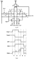
- the present disclosure provides in a third embodiment a pixel driving circuit for driving a first OLED O1 and a second OLED 02.
- Cathodes of the first OLED O1 and the second OLED 02 are both connected to the ground GND.
- the pixel driving circuit includes a first pixel driving unit for controlling the first OLED O1 and a second pixel driving unit for controlling the second OLED 02.
- the first pixel driving unit includes a first driving transistor D1, a first storage capacitor C 1 and a first driving control unit.
- a gate electrode of the first driving transistor D1 is connected to a first end of the first storage capacitor C1.
- the first driving control unit includes: a first control transistor T1, a gate electrode of which is configured to receive a first scanning signal Scan1, a first electrode of which is connected to a first electrode of the first driving transistor D1, and a second electrode of which is connected to the gate electrode of the first driving transistor D1; a second control transistor T2, a gate electrode of which is configured to receive the first scanning signal Scan1, a first electrode of which is connected to a second electrode of the first driving transistor D1, and a second electrode of which is connected to the ground GND; a third control transistor T3, a gate electrode of which is configured to receive a first driving control signal EM1, a first electrode of which is connected to a second end of the first storage capacitor C1, and a second electrode of which is configured to receive a data voltage on a data line Data; and a fourth control transistor T4, a gate electrode of which is configured to receive a second scanning signal Scan2, a first electrode of which is configured to receive a high level Vdd, and a second electrode of which is connected to
- the second electrode of the first driving transistor D1 is connected to an anode of the first OLED O1.
- the cathode of the first OLED O1 is connected to the ground GND.
- the second pixel driving unit includes a second driving transistor D2, a second storage capacitor C2 and a second driving control unit.
- a gate electrode of the second driving transistor D2 is connected to a first end of the second storage capacitor C2.
- the second driving control unit includes: a fifth control transistor T5, a gate electrode of which is configured to receive the first scanning signal Scan1, a first electrode of which is connected to a first electrode of the second driving transistor D2, and a second electrode of which is connected to the gate electrode of the second driving transistor D2; a sixth control transistor T6, a gate electrode of which is configured to receive the first scanning signal Scan1, a first electrode of which is connected to a second electrode of the second driving transistor D2, and a second electrode of which is connected to the ground GND; a seventh control transistor T7, a gate electrode of which is configured to receive a second driving control signal EM2, a first electrode of which is connected to a second end of the second storage capacitor C2, and a second electrode of which is configured to receive the data voltage on the data line Data; and an eighth control transistor T8, a gate electrode of which is configured to receive the second scanning signal Scan2, a first electrode of which is configured to receive the high level Vdd, and a second electrode of which is connected to the first electrode of the
- the second electrode of the second driving transistor D2 is connected to an anode of the second OLED 02.
- the cathode of the second OLED 02 is connected to the ground GND.
- a1 represents a node connected to the first end of C1
- a2 represents a node connected to the first end of C2
- b1 represents a node connected to the second end of C1
- b2 represents a node connected to the second end of C2.
- D1, D2, T1, T2, T3, T4, T5, T6, T7 and T8 are all n-type TFTs, so it is able to manufacture them by an identical process, thereby to improve the yield thereof.
- an oscillogram of Scan2 is a symmetric reversal of an oscillogram of EM2, so it is also able to reduce the number of control signal lines by changing types of the transistors which are configured to receive Scan2 and EM2.
- T7 that should have been configured to receive EM2 in Fig.3A is changed to a p-type TFT, and the gate electrode of T7 is configured to receive the second scanning signal Scan2, so that it is able to reduce the number of the control signals while achieving the purpose of the present disclosure.
- Scan1 and Scan2 are each of a high level
- EM1 and EM2 are each of a low level
- the data voltage Vdata on the data line is V0.
- C1 is charged by Vdd through T4 and T1, so that a1 is at a potential of Vdd and T3 is turned off.
- C2 is charged by Vdd through T8 and T5, so a2 is at a potential of Vdd and T7 is turned off.
- Scan1, EM1 and EM2 are each of a high level, Scan2 is of a low level, and Vdata is V0.
- T1, T2 and T3 are all turned on, and T4 is turned off, so C1 is discharged toward the ground through T1, D1 and T2 until a1 is at a potential of a threshold voltage Vth1 of D1.
- B1 is configured to receive Vdata, so b1 is at a potential of V0.
- Scan1 and Scan2 are each of a low level, EM1 and EM2 are each of a high level, and Vdata is jumped to V0+ ⁇ V1.
- the potential at b1 is jumped from V0 at the second stage to V0+ ⁇ V1 at the third stage.
- the first end of C1 is in a floating state, so a potential Va1 at a1 and a potential Vb1 at b1 are jumped equally (i.e., an original voltage difference Vth1-V0 is maintained).
- a1 is maintained at a potential of ⁇ V1+Vth1.
- the potential of b2 is jumped from V0 at the second stage to V0+ ⁇ V1 at the third stage.
- the first end of C2 is in a floating state, so a potential Va2 at a2 and a potential Vb2 at b2 are jumped equally (i.e., an original voltage difference Vth2-V0 is maintained).
- a2 is maintained at a potential of ⁇ V1+Vth2.
- Scan1, Scan2 and EM1 are each of a low level, EM2 is of a high level, and Vdata is jumped to V0+ ⁇ V2.
- the potential at b2 is jumped from V0+ ⁇ V1 at the third stage to V0+ ⁇ V2 at the fourth stage.
- the first end of C2 is in the floating state, so the potential Va2 at a2 and the potential Vb2 at b2 are jumped equally (i.e., an original voltage difference Vth2-V0 is maintained).
- a2 is maintained at a potential of ⁇ V2+Vth2.
- Scan1, EM1 and EM2 are ach of a low level, and Scan2 is of a high level.
- Scan2 is of a high level.
- the OLED emits light after two voltage compensation stages and two jumping procedures.
- T4 is turned on, the first electrode of D1 is configured to receive the high level Vdd through T4, T2 is turned off, and D1 drives the first OLED O1 to emit light.
- a current flowing through 02 is equal to K( ⁇ V2-Voled2) 2 , where Voled2 represents a potential at the anode of 02.
- the jumping voltage compensation is performed sequentially on a first pixel unit including the first OLED and a second pixel unit including the second OLED, and a jumping signal is applied onto Vdata, i.e., signal superposition and jumping are performed at different time domains, so as to achieve the pixel compensation.
- Vdata i.e., signal superposition and jumping are performed at different time domains.
- it is able to prevent the occurrence of uneven threshold voltages of the driving TFTs for the two pixel units due to limitations of the manufacture process and a long-term operation, and prevent the currents flowing through the OLEDS included in the two pixel units from being adversely affected by the threshold voltages of the driving transistors, thereby to ensure the even image display.
- no current flows through the OLED at the charging stage, the discharging stage, the first compensation stage and the second compensation stage so it is able to prolong a service life of the OLED.
- V0, ⁇ V1 and ⁇ V2 are greater than 0, and ⁇ V2 is greater than ⁇ V1.
- the present disclosure provides in a sixth embodiment a pixel driving circuit for driving a first light-emitting element and a second light-emitting element. First ends of the first light-emitting element and the second light-emitting element are configured to receive a first level.
- the pixel driving circuit includes a first pixel driving unit and a second pixel driving unit.
- the first pixel driving unit includes a first driving transistor, a first storage capacitor and a first driving control unit.
- a first end of the first storage capacitor is connected to a gate electrode of the first driving transistor, and a second end thereof is configured to receive a data voltage through the first driving control unit.
- the gate electrode of the first driving transistor is connected to a first electrode of the first driving transistor through the first driving control unit, the first electrode thereof is connected to a second end of the first light-emitting element through the first driving control unit, and a second electrode thereof is configured to receive a second level through the first driving control unit.
- the second pixel driving unit includes a second driving transistor, a second storage capacitor and a second driving control unit.
- a first end of the second storage capacitor is connected to a gate electrode of the second driving transistor, and a second end thereof is configured to receive the data voltage through the second driving control unit.
- the gate electrode of the second driving transistor is connected to a first electrode of the second driving transistor through the second driving control unit, the first electrode thereof is connected to a second end of the second light-emitting element through the second driving control unit, and a second electrode thereof is configured to receive the second level through the second driving control unit.
- the second driving control unit is configured to reset and charge the second storage capacitor through the second level and the data voltage, so as to apply a jumping voltage onto the data voltage at a second compensation stage, thereby to perform jumping compensation on a threshold voltage of the second driving transistor and control the second driving transistor to drive the second light-emitting element to emit light.
- two adjacent pixel driving units having a threshold voltage compensation function in the related art are combined so as to share a single data line, thereby it is able to control two pixel units to perform jumping compensation on the threshold voltage of the driving transistor at the corresponding compensation stage through one pixel driving circuit having the threshold voltage compensation function, and to reduce the number of the TFTs desired for the threshold voltage compensation as well as the number of the data lines.
- it is able to remarkably increase an aperture ratio of the pixel unit and reduce the production cost, thereby to improve the image quality and the PPI.
- the light-emitting element may be an OLED.
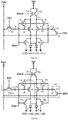
- the present disclosure provides in a seventh embodiment a pixel driving circuit for driving a first OLED O1 and a second OLED 02.
- Cathodes of the first OLED O1 and the second OLED 02 are configured to receive a first level V1.
- the pixel driving circuit includes a first pixel driving unit for controlling the first OLED O1 and a second pixel driving unit for controlling the second OLED 02.
- the first pixel driving unit includes a first driving transistor D1, a first storage capacitor C 1 and a first driving control unit 61.
- a first end of the first storage capacitor C1 is connected to a gate electrode of the first driving transistor D1, and a second end thereof is configured to receive a data voltage on a data line Data through the first driving control unit 61.
- the gate electrode of the first driving transistor D1 is connected to a first electrode of the first driving transistor D1 through the first driving control unit 61, the first electrode thereof is connected to an anode of the first OLED O1 through the first driving control unit 61, and a second electrode thereof is configured to receive a second level V2 through the first driving control unit 61.
- the second pixel driving unit includes a second driving transistor D2, a second storage capacitor C2 and a second driving control unit 62.
- a first end of the second storage capacitor C2 is connected to a gate electrode of the second driving transistor D2, and a second end thereof is configured to receive the data voltage on the data line Data through the second driving control unit 62.
- the gate electrode of the second driving transistor D2 is connected to a first electrode of the second driving transistor D2 through the second driving control unit 62, the first electrode thereof is connected to an anode of the second OLED 02 through the second driving control unit 62, and a second electrode thereof is configured to receive the second level V2 through the second driving control unit 62.
- D1 and D2 are both p-type TFTs, and at this time, the first level V1 is a low level and the second level V2 is a high level.
- the first driving control unit may be of a structure identical to the second driving control unit.
- the first driving control unit includes: a first control transistor, a gate electrode of which is configured to receive a first driving control signal, a first electrode of which is connected to the first electrode of the first driving transistor, and a second electrode of which is connected to the gate electrode of the first driving transistor; a second control transistor, a gate electrode of which is configured to receive the first driving control signal, a first electrode of which is configured to receive the data voltage, and a second electrode of which is connected to the second end of the first storage capacitor; a third control transistor, a gate electrode of which is configured to receive a first scanning signal, a first electrode of which is connected to the second electrode of the first driving transistor, and a second electrode of which is configured to receive the second level; and a fourth control transistor, a gate electrode of which is configured to receive a second scanning signal, a first electrode of which is connected to the second end of the first light-emitting element, and a second electrode of which is connected to the first electrode of the first driving transistor.
- the second driving control unit includes: a fifth control transistor, a gate electrode of which is configured to receive a second driving control signal, a first electrode of which is connected to the first electrode of the second driving transistor, and a second electrode of which is connected to the gate electrode of the second driving transistor; a sixth control transistor, a gate electrode of which is configured to receive the second driving control signal, a first electrode of which is configured to receive the data voltage, and a second electrode of which is connected to the second end of the second storage capacitor; a seventh control transistor, a gate electrode of which is configured to receive the first scanning signal, a first electrode of which is connected to the second electrode of the second driving transistor, and a second electrode of which is configured to receive the second level; and an eighth control transistor, a gate electrode of which is configured to receive the second scanning signal, a first electrode of which is connected to the second end of the second light-emitting element, and a second electrode of which is connected to the first electrode of the second driving transistor.
- the first driving transistor, the first control transistor, the second control transistor, the third control transistor and the fourth control transistor are all p-type TFTs
- the second driving transistor, the fifth control transistor, the sixth control transistor, the seventh control transistor and the eighth control transistor are all p-type TFTs.
- the present disclosure provides in an eighth embodiment a pixel driving circuit for driving a first OLED O1 and a second OLED 02.
- Cathodes of the first OLED O1 and the second OLED 02 are both connected to the ground GND.
- the pixel driving circuit includes a first pixel driving unit for controlling the first OLED O1 and a second pixel driving unit for controlling the second OLED 02.
- the first pixel driving unit includes a first driving transistor D1, a first storage capacitor C 1 and a first driving control unit. A first end a1 of the storage capacitor C1 is connected to a gate electrode of the first driving transistor D1.
- the first driving control unit includes: a first control transistor T1, a first electrode of which is connected to a first electrode of the first driving transistor D1, and a second electrode of which is connected to the gate electrode of the first driving transistor D1; a second control transistor T2, a first electrode of which is configured to receive a data voltage on a data line Data, and a second electrode of which is connected to a second end b1 of the first storage capacitor C1; a third control transistor T3, a gate electrode of which is configured to receive a first scanning signal Scan1, a first electrode of which is connected to a second electrode of the first driving transistor D1, and a second electrode of which is configured to receive a high level Vdd; and a fourth control transistor T4, a gate electrode of which is configured to receive a second scanning signal Scan2, a first electrode of which is connected to an anode of the first OLED O1, and a second electrode of which is connected to the first electrode of the first driving transistor D1.
- the second pixel driving unit includes a second driving transistor D2, a second storage capacitor C2 and a second driving control unit. A first end a2 of the second storage capacitor C2 is connected to a gate electrode of the second driving transistor D2.
- the second driving control unit includes: a fifth control transistor T5, a first electrode of which is connected to a first electrode of the second driving transistor D2, and a second electrode of which is connected to the gate electrode of the second driving transistor D2; a sixth control transistor T6, a first electrode of which is configured to receive the data voltage on the data line Data, and a second electrode of which is connected to a second end b2 of the second storage capacitor C2; a seventh control transistor T7, a gate electrode of which is configured to the first scanning signal Scan1, a first electrode of which is connected to a second electrode of the second driving transistor D2, and a second electrode of which is configured to receive the high level Vdd; and an eighth control transistor T8, a gate electrode of which is configured to receive the second scanning signal Scan2, a first electrode of which is connected to an anode of the second OLED 02, and a second electrode of which is connected to the first electrode of the second driving transistor D2.
- the gate electrodes T1 and T2 are both configured to receive a third scanning signal Scan3, and in the second driving control unit, the gate electrodes of T5 and T6 are both configured to receive a fourth scanning signal Scan4.
- T1, T2, T3, T4, T5, T6, T7, T8, D1 and D2 are all p-type TFTs.
- all the TFTs are p-type TFTs, so as to manufacture them by an identical process, thereby to improve the yield thereof.
- the two pixel driving units having the threshold compensation function are combined within one pixel driving circuit, and controlled by only one data line Data.
- T1, T2, T3, T4, T5, T6, T7 and T8 are all switching TFTs
- D1 and D2 are driving TFTs for the pixels
- Scan1, Scan2, Scan3 and Scan4 are all scanning signals for controlling an on or off state of the switching TFTs.
- Scan1, Scan3 and Scan4 are each a low level, and Scan2 is a high level.
- the TFTs other than T4 and T8 are turned on, and a1 is charged by Vdd through T3, D1 and T1 until a potential at a1 reaches Vdd-Vth1 (i.e., a voltage difference between a gate electrode and a source electrode of D1 is a threshold voltage Vth1 of D1).
- b1 is configured to receive the data voltage Vdata and a potential at b1 is ⁇ V1, so after the charging is completed, a potential difference between the two ends of C1 is always maintained at Vdd-Vth1- ⁇ V1.
- T4 is turned off, no current flows through O1, and as a result, it is able to indirectly prolong a service life of O1.
- a potential different between the two ends of C1 in the other pixel driving unit is always maintained at Vdd-Vth2- ⁇ V1, where Vth2 is a threshold of D2.
- Scan1 and Scan2 are each a high level
- Scan3 and Scan4 are each a low level.
- Vdata is jumped from ⁇ V1 at the first stage to ⁇ V2 at the second stage (V2 is greater than V1) and a1 is in a floating state, so a potential Va1 at a1 and a potential Vb1 at b1 are jumped equally (an original potential difference Vdd-Vth1-V1 is maintained).
- the potential Va1 at a1 is maintained at Vdd-Vth1+ ⁇ V2- ⁇ V1.
- the potential Va2 at a2 is maintained at Vdd-Vth2+ ⁇ V2- ⁇ V1.
- Scan1, Scan2 and Scan3 are each a high level, and Scan4 is a low level.
- Vdata is jumped to V3 (V3 is greater than V2), and the potential Vb2 at the second end b2 of C2 is jumped from ⁇ V2 to ⁇ V3. Because a2 is in the floating state, Va2 and Vb2 are jumped equally (an original potential difference Vdd-Vth2- ⁇ V1 is maintained). At this time, the potential Va2 at a2 is maintained at Vdd-Vth2+ ⁇ V3- ⁇ V1.
- Scan1 and Scan2 are ach a low level
- Scan3 and Scan4 are each a high level.
- the OLED emits light after two voltage compensation stages and two jumping procedures
- Fig.9D shows the on states of the TFTs.
- An operating voltage is Vdd, and the two pixels emit light through the respective paths.
- a current I O2 flowing through 02 is K( ⁇ V3- ⁇ V1) 2 .
- the jumping voltage compensation is performed sequentially on a first pixel unit including the first OLED and a second pixel unit including the second OLED, and a jumping signal is applied onto Vdata, i.e., signal superposition and jumping are performed at different time domains, so as to achieve the pixel compensation.
- Vdata i.e., signal superposition and jumping are performed at different time domains.
- it is able to prevent the occurrence of uneven threshold voltages of the driving TFTs for the two pixel units due to limitations of the manufacture process and a long-term operation, and prevent the currents flowing through the OLEDS included in the two pixel units from being adversely affected by the threshold voltages of the driving transistors, thereby to ensure the even image display.
- the present disclosure further provides in one embodiment a pixel driving method for driving the pixel driving circuit according to the fifth, sixth or seventh embodiment, which includes steps of:
- the driving transistors included in the pixel driving circuit are all p-type TFTs, ⁇ V1, ⁇ V2 and ⁇ V3 are greater than 0, ⁇ V3 is greater than ⁇ V2, and ⁇ V2 is greater than ⁇ V1.
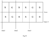
- the pixel driving circuit as shown in Fig.10 is arranged in two adjacent pixel units, and these two adjacent pixel units share a single data line.
- the pixel driving circuit may be arranged in a red pixel unit R and a green pixel unit G adjacent to each other, or in a green pixel unit G and a blue pixel unit B adjacent to each other.
- the present disclosure further provides in one embodiment a display panel including the above-mentioned pixel driving circuit.
- the present disclosure further provides in one embodiment a display device including the above-mentioned display panel.
- the display device may be an AMOLED display device.
- the pixel driving circuit, the display panel and the display device in the embodiments of the present disclosure may be manufactured by a low temperature polysilicon (LTPS) technique, or an a-Si technique.
- LTPS low temperature polysilicon
- the pixel driving circuit in the embodiments of the present disclosure may include a-Si, poly-Si or oxide TFTs, and the types of the TFTs in the pixel driving circuit may be changed in accordance with the practical need.
- the above description is given by taking AMOLED as an example, the present disclosure is not limited thereto, and any other light-emitting diodes may also be used.
Landscapes
- Engineering & Computer Science (AREA)
- Physics & Mathematics (AREA)
- Computer Hardware Design (AREA)
- General Physics & Mathematics (AREA)
- Theoretical Computer Science (AREA)
- Control Of Indicators Other Than Cathode Ray Tubes (AREA)
- Control Of El Displays (AREA)
- Electroluminescent Light Sources (AREA)
Priority Applications (1)
| Application Number | Priority Date | Filing Date | Title |
|---|---|---|---|
| EP19187202.7A EP3576080B1 (de) | 2014-09-25 | 2015-01-23 | Pixeltreiberschaltung, pixelansteuerungsverfahren, anzeigetafel und anzeigevorrichtung |
Applications Claiming Priority (2)
| Application Number | Priority Date | Filing Date | Title |
|---|---|---|---|
| CN201410498525.2A CN104252845B (zh) | 2014-09-25 | 2014-09-25 | 像素驱动电路、方法、显示面板和显示装置 |
| PCT/CN2015/071406 WO2016045283A1 (zh) | 2014-09-25 | 2015-01-23 | 像素驱动电路、方法、显示面板和显示装置 |
Related Child Applications (2)
| Application Number | Title | Priority Date | Filing Date |
|---|---|---|---|
| EP19187202.7A Division EP3576080B1 (de) | 2014-09-25 | 2015-01-23 | Pixeltreiberschaltung, pixelansteuerungsverfahren, anzeigetafel und anzeigevorrichtung |
| EP19187202.7A Division-Into EP3576080B1 (de) | 2014-09-25 | 2015-01-23 | Pixeltreiberschaltung, pixelansteuerungsverfahren, anzeigetafel und anzeigevorrichtung |
Publications (3)
| Publication Number | Publication Date |
|---|---|
| EP3200178A1 true EP3200178A1 (de) | 2017-08-02 |
| EP3200178A4 EP3200178A4 (de) | 2018-10-03 |
| EP3200178B1 EP3200178B1 (de) | 2022-08-24 |
Family
ID=52187692
Family Applications (2)
| Application Number | Title | Priority Date | Filing Date |
|---|---|---|---|
| EP15748154.0A Active EP3200178B1 (de) | 2014-09-25 | 2015-01-23 | Pixeltreiberschaltung, verfahren, anzeigetafel und anzeigevorrichtung |
| EP19187202.7A Active EP3576080B1 (de) | 2014-09-25 | 2015-01-23 | Pixeltreiberschaltung, pixelansteuerungsverfahren, anzeigetafel und anzeigevorrichtung |
Family Applications After (1)
| Application Number | Title | Priority Date | Filing Date |
|---|---|---|---|
| EP19187202.7A Active EP3576080B1 (de) | 2014-09-25 | 2015-01-23 | Pixeltreiberschaltung, pixelansteuerungsverfahren, anzeigetafel und anzeigevorrichtung |
Country Status (4)
| Country | Link |
|---|---|
| US (1) | US9640109B2 (de) |
| EP (2) | EP3200178B1 (de) |
| CN (1) | CN104252845B (de) |
| WO (1) | WO2016045283A1 (de) |
Families Citing this family (33)
| Publication number | Priority date | Publication date | Assignee | Title |
|---|---|---|---|---|
| CN103531149B (zh) * | 2013-10-31 | 2015-07-15 | 京东方科技集团股份有限公司 | 一种交流驱动的像素电路、驱动方法及显示装置 |
| CN104252845B (zh) * | 2014-09-25 | 2017-02-15 | 京东方科技集团股份有限公司 | 像素驱动电路、方法、显示面板和显示装置 |
| CN104318898B (zh) * | 2014-11-11 | 2017-12-08 | 京东方科技集团股份有限公司 | 像素电路、驱动方法和显示装置 |
| CN104361862A (zh) * | 2014-11-28 | 2015-02-18 | 京东方科技集团股份有限公司 | 阵列基板及其驱动方法、显示面板、显示装置 |
| CN205080892U (zh) * | 2015-09-28 | 2016-03-09 | 合肥鑫晟光电科技有限公司 | 像素驱动电路、像素电路、显示面板和显示装置 |
| US10600363B2 (en) | 2016-02-04 | 2020-03-24 | Shanghai Tianma AM-OLED Co., Ltd. | Method for driving an array substrate having a plurality of light emitting components |
| CN105528997B (zh) | 2016-02-04 | 2018-09-21 | 上海天马有机发光显示技术有限公司 | 一种像素电路、驱动方法以及显示面板 |
| CN106097959A (zh) * | 2016-06-02 | 2016-11-09 | 京东方科技集团股份有限公司 | 像素单元及其驱动方法、像素驱动电路和显示装置 |
| CN105895028B (zh) | 2016-06-30 | 2018-12-14 | 京东方科技集团股份有限公司 | 一种像素电路及驱动方法和显示设备 |
| CN106251810B (zh) * | 2016-08-19 | 2019-09-27 | 深圳市华星光电技术有限公司 | Amoled显示屏驱动方法、驱动电路及显示装置 |
| CN107818759B (zh) * | 2016-09-14 | 2023-09-19 | 合肥鑫晟光电科技有限公司 | 像素驱动电路及像素驱动方法、阵列基板以及显示装置 |
| CN106409221B (zh) * | 2016-10-31 | 2019-05-31 | 昆山国显光电有限公司 | 多面显示像素电路及其驱动方法、多面oled显示器 |
| CN106611586B (zh) | 2017-03-08 | 2018-11-13 | 京东方科技集团股份有限公司 | 像素驱动电路、驱动方法、有机发光显示面板及显示装置 |
| CN106971691A (zh) * | 2017-05-31 | 2017-07-21 | 京东方科技集团股份有限公司 | 一种像素电路、驱动方法及显示装置 |
| US10210799B2 (en) * | 2017-06-28 | 2019-02-19 | Wuhan China Star Optoelectronics Semiconductor Display Technology Co., Ltd. | Pixel compensation circuit and display device |
| CN107230455A (zh) * | 2017-07-21 | 2017-10-03 | 京东方科技集团股份有限公司 | 一种像素驱动电路、像素驱动方法和显示基板 |
| CN107886901B (zh) * | 2017-12-04 | 2019-10-18 | 合肥鑫晟光电科技有限公司 | 像素驱动电路、显示面板及其驱动方法 |
| CN110400536B (zh) * | 2018-04-23 | 2020-12-25 | 上海和辉光电股份有限公司 | 一种像素电路及其驱动方法、显示面板 |
| CN108717841B (zh) | 2018-05-29 | 2020-07-28 | 京东方科技集团股份有限公司 | 像素驱动电路、像素驱动方法、oled显示面板及其驱动电路和驱动方法 |
| CN108806612B (zh) * | 2018-06-13 | 2020-01-10 | 京东方科技集团股份有限公司 | 像素电路及其驱动方法、显示装置 |
| CN110060631B (zh) * | 2018-06-27 | 2021-09-03 | 友达光电股份有限公司 | 像素电路 |
| TWI694433B (zh) * | 2018-06-27 | 2020-05-21 | 友達光電股份有限公司 | 畫素電路 |
| CN109545145B (zh) * | 2019-01-02 | 2020-07-28 | 京东方科技集团股份有限公司 | 像素电路及其驱动方法、显示装置 |
| CN109658866B (zh) * | 2019-03-04 | 2020-06-30 | 上海大学 | 一种高密度像素驱动电路及其驱动方法 |
| CN109801593B (zh) * | 2019-03-28 | 2020-06-23 | 京东方科技集团股份有限公司 | 一种驱动电路、显示面板和驱动方法 |
| CN110047435B (zh) * | 2019-04-23 | 2020-12-04 | 京东方科技集团股份有限公司 | 像素驱动电路及其驱动方法、显示面板和显示装置 |
| CN110379372B (zh) * | 2019-08-30 | 2021-01-26 | 京东方科技集团股份有限公司 | 像素驱动单元、电路、方法、显示面板和显示装置 |
| TWI716120B (zh) * | 2019-09-25 | 2021-01-11 | 友達光電股份有限公司 | 畫素電路與顯示面板 |
| TWI714317B (zh) * | 2019-10-23 | 2020-12-21 | 友達光電股份有限公司 | 畫素電路與相關的顯示裝置 |
| CN111540303A (zh) * | 2020-01-17 | 2020-08-14 | 重庆康佳光电技术研究院有限公司 | 一种驱动电路及显示装置 |
| CN115881039A (zh) * | 2021-09-27 | 2023-03-31 | 乐金显示有限公司 | 像素电路和包括该像素电路的显示装置 |
| JP2023050791A (ja) * | 2021-09-30 | 2023-04-11 | セイコーエプソン株式会社 | 電気光学装置、電子機器および電気光学装置の駆動方法 |
| CN114267297B (zh) * | 2021-12-16 | 2023-05-02 | Tcl华星光电技术有限公司 | 像素补偿电路、方法及显示面板 |
Family Cites Families (11)
| Publication number | Priority date | Publication date | Assignee | Title |
|---|---|---|---|---|
| US7196682B2 (en) * | 2003-09-29 | 2007-03-27 | Wintek Corporation | Driving apparatus and method for active matrix organic light emitting display |
| TWI371018B (en) * | 2006-05-09 | 2012-08-21 | Chimei Innolux Corp | System for displaying image and driving display element method |
| EP1857998A1 (de) * | 2006-05-19 | 2007-11-21 | TPO Displays Corp. | System zur Bildanzeige und Verfahren zur Ansteuerung eines Anzeigeelements |
| CN103474025B (zh) * | 2013-09-06 | 2015-07-01 | 京东方科技集团股份有限公司 | 一种像素电路及显示器 |
| CN104036729B (zh) * | 2014-06-09 | 2017-03-08 | 京东方科技集团股份有限公司 | 像素驱动电路及其驱动方法、显示装置 |
| CN104036731B (zh) * | 2014-06-13 | 2016-03-23 | 京东方科技集团股份有限公司 | 像素电路和显示装置 |
| CN104078004B (zh) | 2014-06-18 | 2016-08-31 | 京东方科技集团股份有限公司 | 像素电路和显示装置 |
| CN104050919B (zh) * | 2014-06-18 | 2016-03-16 | 京东方科技集团股份有限公司 | 像素电路和显示装置 |
| CN104134426B (zh) * | 2014-07-07 | 2017-02-15 | 京东方科技集团股份有限公司 | 像素结构及其驱动方法、显示装置 |
| CN104252845B (zh) * | 2014-09-25 | 2017-02-15 | 京东方科技集团股份有限公司 | 像素驱动电路、方法、显示面板和显示装置 |
| CN104361862A (zh) * | 2014-11-28 | 2015-02-18 | 京东方科技集团股份有限公司 | 阵列基板及其驱动方法、显示面板、显示装置 |
-
2014
- 2014-09-25 CN CN201410498525.2A patent/CN104252845B/zh active Active
-
2015
- 2015-01-23 WO PCT/CN2015/071406 patent/WO2016045283A1/zh active Application Filing
- 2015-01-23 EP EP15748154.0A patent/EP3200178B1/de active Active
- 2015-01-23 US US14/769,346 patent/US9640109B2/en active Active
- 2015-01-23 EP EP19187202.7A patent/EP3576080B1/de active Active
Also Published As
| Publication number | Publication date |
|---|---|
| US9640109B2 (en) | 2017-05-02 |
| US20160253963A1 (en) | 2016-09-01 |
| CN104252845A (zh) | 2014-12-31 |
| CN104252845B (zh) | 2017-02-15 |
| EP3576080B1 (de) | 2021-09-29 |
| EP3576080A1 (de) | 2019-12-04 |
| EP3200178B1 (de) | 2022-08-24 |
| EP3200178A4 (de) | 2018-10-03 |
| WO2016045283A1 (zh) | 2016-03-31 |
Similar Documents
| Publication | Publication Date | Title |
|---|---|---|
| EP3200178B1 (de) | Pixeltreiberschaltung, verfahren, anzeigetafel und anzeigevorrichtung | |
| KR102079839B1 (ko) | 표시 장치, 표시 장치의 구동 방법 및 전자 기기 | |
| US9842546B2 (en) | Organic light emitting display device for improving a contrast ratio | |
| US10504436B2 (en) | Pixel driving circuits, pixel driving methods and display devices | |
| EP1291839B1 (de) | Schaltung und Verfahren zum Treiben einer stromgesteuerten Vorrichtung | |
| US9852687B2 (en) | Display device and driving method | |
| US9564082B2 (en) | Array substrate, display device and driving method thereof | |
| US11341916B2 (en) | Display apparatus having varied driving frequency and gate clock signal | |
| US11127342B2 (en) | Pixel circuit for driving light emitting diode to emit light and method of controlling the pixel circuit | |
| EP2581899A2 (de) | Lichtemittierende Anzeigevorrichtung | |
| US20180218677A1 (en) | Pixel driving circuit, display apparatus and driving method thereof | |
| US9633598B2 (en) | Pixel circuit and driving method thereof | |
| US20090295772A1 (en) | Pixel and organic light emitting display using the same | |
| EP3048603B1 (de) | Pixeleinheitstreiberschaltung, pixeleinheitsantriebsverfahren, pixeleinheit und anzeigevorrichtung | |
| CN110164378B (zh) | Amoled像素电路及其驱动方法 | |
| CN109166522B (zh) | 像素电路、其驱动方法及显示装置 | |
| US20070195019A1 (en) | Image display apparatus | |
| KR20140071236A (ko) | 표시 장치 및 구동 방법 | |
| US8922541B2 (en) | Method of driving display device | |
| US11094252B2 (en) | Display-driving method and a display apparatus | |
| JP5414808B2 (ja) | 表示装置およびその駆動方法 | |
| CN109192139B (zh) | 一种像素补偿电路 | |
| US8289309B2 (en) | Inverter circuit and display | |
| US20100103162A1 (en) | Image display apparatus and method of driving the image display apparatus | |
| KR20140022345A (ko) | 표시 장치, 전자 기기, 구동 방법 및 구동 회로 |
Legal Events
| Date | Code | Title | Description |
|---|---|---|---|
| PUAI | Public reference made under article 153(3) epc to a published international application that has entered the european phase |
Free format text: ORIGINAL CODE: 0009012 |
|
| STAA | Information on the status of an ep patent application or granted ep patent |
Free format text: STATUS: REQUEST FOR EXAMINATION WAS MADE |
|
| 17P | Request for examination filed |
Effective date: 20150820 |
|
| AK | Designated contracting states |
Kind code of ref document: A1 Designated state(s): AL AT BE BG CH CY CZ DE DK EE ES FI FR GB GR HR HU IE IS IT LI LT LU LV MC MK MT NL NO PL PT RO RS SE SI SK SM TR |
|
| AX | Request for extension of the european patent |
Extension state: BA ME |
|
| DAX | Request for extension of the european patent (deleted) | ||
| RIC1 | Information provided on ipc code assigned before grant |
Ipc: G09G 3/32 20160101AFI20180119BHEP |
|
| A4 | Supplementary search report drawn up and despatched |
Effective date: 20180830 |
|
| RIC1 | Information provided on ipc code assigned before grant |
Ipc: G09G 3/32 20160101AFI20180824BHEP |
|
| STAA | Information on the status of an ep patent application or granted ep patent |
Free format text: STATUS: EXAMINATION IS IN PROGRESS |
|
| 17Q | First examination report despatched |
Effective date: 20190409 |
|
| STAA | Information on the status of an ep patent application or granted ep patent |
Free format text: STATUS: EXAMINATION IS IN PROGRESS |
|
| STAA | Information on the status of an ep patent application or granted ep patent |
Free format text: STATUS: EXAMINATION IS IN PROGRESS |
|
| GRAP | Despatch of communication of intention to grant a patent |
Free format text: ORIGINAL CODE: EPIDOSNIGR1 |
|
| STAA | Information on the status of an ep patent application or granted ep patent |
Free format text: STATUS: GRANT OF PATENT IS INTENDED |
|
| INTG | Intention to grant announced |
Effective date: 20220511 |
|
| GRAS | Grant fee paid |
Free format text: ORIGINAL CODE: EPIDOSNIGR3 |
|
| GRAA | (expected) grant |
Free format text: ORIGINAL CODE: 0009210 |
|
| STAA | Information on the status of an ep patent application or granted ep patent |
Free format text: STATUS: THE PATENT HAS BEEN GRANTED |
|
| AK | Designated contracting states |
Kind code of ref document: B1 Designated state(s): AL AT BE BG CH CY CZ DE DK EE ES FI FR GB GR HR HU IE IS IT LI LT LU LV MC MK MT NL NO PL PT RO RS SE SI SK SM TR |
|
| REG | Reference to a national code |
Ref country code: CH Ref legal event code: EP |
|
| REG | Reference to a national code |
Ref country code: IE Ref legal event code: FG4D |
|
| REG | Reference to a national code |
Ref country code: AT Ref legal event code: REF Ref document number: 1514204 Country of ref document: AT Kind code of ref document: T Effective date: 20220915 Ref country code: DE Ref legal event code: R096 Ref document number: 602015080463 Country of ref document: DE |
|
| REG | Reference to a national code |
Ref country code: LT Ref legal event code: MG9D |
|
| REG | Reference to a national code |
Ref country code: NL Ref legal event code: MP Effective date: 20220824 |
|
| PG25 | Lapsed in a contracting state [announced via postgrant information from national office to epo] |
Ref country code: SE Free format text: LAPSE BECAUSE OF FAILURE TO SUBMIT A TRANSLATION OF THE DESCRIPTION OR TO PAY THE FEE WITHIN THE PRESCRIBED TIME-LIMIT Effective date: 20220824 Ref country code: RS Free format text: LAPSE BECAUSE OF FAILURE TO SUBMIT A TRANSLATION OF THE DESCRIPTION OR TO PAY THE FEE WITHIN THE PRESCRIBED TIME-LIMIT Effective date: 20220824 Ref country code: PT Free format text: LAPSE BECAUSE OF FAILURE TO SUBMIT A TRANSLATION OF THE DESCRIPTION OR TO PAY THE FEE WITHIN THE PRESCRIBED TIME-LIMIT Effective date: 20221226 Ref country code: NO Free format text: LAPSE BECAUSE OF FAILURE TO SUBMIT A TRANSLATION OF THE DESCRIPTION OR TO PAY THE FEE WITHIN THE PRESCRIBED TIME-LIMIT Effective date: 20221124 Ref country code: NL Free format text: LAPSE BECAUSE OF FAILURE TO SUBMIT A TRANSLATION OF THE DESCRIPTION OR TO PAY THE FEE WITHIN THE PRESCRIBED TIME-LIMIT Effective date: 20220824 Ref country code: LV Free format text: LAPSE BECAUSE OF FAILURE TO SUBMIT A TRANSLATION OF THE DESCRIPTION OR TO PAY THE FEE WITHIN THE PRESCRIBED TIME-LIMIT Effective date: 20220824 Ref country code: LT Free format text: LAPSE BECAUSE OF FAILURE TO SUBMIT A TRANSLATION OF THE DESCRIPTION OR TO PAY THE FEE WITHIN THE PRESCRIBED TIME-LIMIT Effective date: 20220824 Ref country code: FI Free format text: LAPSE BECAUSE OF FAILURE TO SUBMIT A TRANSLATION OF THE DESCRIPTION OR TO PAY THE FEE WITHIN THE PRESCRIBED TIME-LIMIT Effective date: 20220824 Ref country code: ES Free format text: LAPSE BECAUSE OF FAILURE TO SUBMIT A TRANSLATION OF THE DESCRIPTION OR TO PAY THE FEE WITHIN THE PRESCRIBED TIME-LIMIT Effective date: 20220824 |
|
| REG | Reference to a national code |
Ref country code: AT Ref legal event code: MK05 Ref document number: 1514204 Country of ref document: AT Kind code of ref document: T Effective date: 20220824 |
|
| PG25 | Lapsed in a contracting state [announced via postgrant information from national office to epo] |
Ref country code: PL Free format text: LAPSE BECAUSE OF FAILURE TO SUBMIT A TRANSLATION OF THE DESCRIPTION OR TO PAY THE FEE WITHIN THE PRESCRIBED TIME-LIMIT Effective date: 20220824 Ref country code: IS Free format text: LAPSE BECAUSE OF FAILURE TO SUBMIT A TRANSLATION OF THE DESCRIPTION OR TO PAY THE FEE WITHIN THE PRESCRIBED TIME-LIMIT Effective date: 20221224 Ref country code: HR Free format text: LAPSE BECAUSE OF FAILURE TO SUBMIT A TRANSLATION OF THE DESCRIPTION OR TO PAY THE FEE WITHIN THE PRESCRIBED TIME-LIMIT Effective date: 20220824 Ref country code: GR Free format text: LAPSE BECAUSE OF FAILURE TO SUBMIT A TRANSLATION OF THE DESCRIPTION OR TO PAY THE FEE WITHIN THE PRESCRIBED TIME-LIMIT Effective date: 20221125 |
|
| PG25 | Lapsed in a contracting state [announced via postgrant information from national office to epo] |
Ref country code: SM Free format text: LAPSE BECAUSE OF FAILURE TO SUBMIT A TRANSLATION OF THE DESCRIPTION OR TO PAY THE FEE WITHIN THE PRESCRIBED TIME-LIMIT Effective date: 20220824 Ref country code: RO Free format text: LAPSE BECAUSE OF FAILURE TO SUBMIT A TRANSLATION OF THE DESCRIPTION OR TO PAY THE FEE WITHIN THE PRESCRIBED TIME-LIMIT Effective date: 20220824 Ref country code: DK Free format text: LAPSE BECAUSE OF FAILURE TO SUBMIT A TRANSLATION OF THE DESCRIPTION OR TO PAY THE FEE WITHIN THE PRESCRIBED TIME-LIMIT Effective date: 20220824 Ref country code: CZ Free format text: LAPSE BECAUSE OF FAILURE TO SUBMIT A TRANSLATION OF THE DESCRIPTION OR TO PAY THE FEE WITHIN THE PRESCRIBED TIME-LIMIT Effective date: 20220824 Ref country code: AT Free format text: LAPSE BECAUSE OF FAILURE TO SUBMIT A TRANSLATION OF THE DESCRIPTION OR TO PAY THE FEE WITHIN THE PRESCRIBED TIME-LIMIT Effective date: 20220824 |
|
| REG | Reference to a national code |
Ref country code: DE Ref legal event code: R097 Ref document number: 602015080463 Country of ref document: DE |
|
| PG25 | Lapsed in a contracting state [announced via postgrant information from national office to epo] |
Ref country code: SK Free format text: LAPSE BECAUSE OF FAILURE TO SUBMIT A TRANSLATION OF THE DESCRIPTION OR TO PAY THE FEE WITHIN THE PRESCRIBED TIME-LIMIT Effective date: 20220824 Ref country code: EE Free format text: LAPSE BECAUSE OF FAILURE TO SUBMIT A TRANSLATION OF THE DESCRIPTION OR TO PAY THE FEE WITHIN THE PRESCRIBED TIME-LIMIT Effective date: 20220824 |
|
| PG25 | Lapsed in a contracting state [announced via postgrant information from national office to epo] |
Ref country code: AL Free format text: LAPSE BECAUSE OF FAILURE TO SUBMIT A TRANSLATION OF THE DESCRIPTION OR TO PAY THE FEE WITHIN THE PRESCRIBED TIME-LIMIT Effective date: 20220824 |
|
| PLBE | No opposition filed within time limit |
Free format text: ORIGINAL CODE: 0009261 |
|
| STAA | Information on the status of an ep patent application or granted ep patent |
Free format text: STATUS: NO OPPOSITION FILED WITHIN TIME LIMIT |
|
| 26N | No opposition filed |
Effective date: 20230525 |
|
| PG25 | Lapsed in a contracting state [announced via postgrant information from national office to epo] |
Ref country code: SI Free format text: LAPSE BECAUSE OF FAILURE TO SUBMIT A TRANSLATION OF THE DESCRIPTION OR TO PAY THE FEE WITHIN THE PRESCRIBED TIME-LIMIT Effective date: 20220824 |
|
| REG | Reference to a national code |
Ref country code: CH Ref legal event code: PL |
|
| GBPC | Gb: european patent ceased through non-payment of renewal fee |
Effective date: 20230123 |
|
| PG25 | Lapsed in a contracting state [announced via postgrant information from national office to epo] |
Ref country code: LU Free format text: LAPSE BECAUSE OF NON-PAYMENT OF DUE FEES Effective date: 20230123 |
|
| REG | Reference to a national code |
Ref country code: BE Ref legal event code: MM Effective date: 20230131 |
|
| PG25 | Lapsed in a contracting state [announced via postgrant information from national office to epo] |
Ref country code: LI Free format text: LAPSE BECAUSE OF NON-PAYMENT OF DUE FEES Effective date: 20230131 Ref country code: GB Free format text: LAPSE BECAUSE OF NON-PAYMENT OF DUE FEES Effective date: 20230123 Ref country code: CH Free format text: LAPSE BECAUSE OF NON-PAYMENT OF DUE FEES Effective date: 20230131 |
|
| PG25 | Lapsed in a contracting state [announced via postgrant information from national office to epo] |
Ref country code: FR Free format text: LAPSE BECAUSE OF NON-PAYMENT OF DUE FEES Effective date: 20230131 Ref country code: BE Free format text: LAPSE BECAUSE OF NON-PAYMENT OF DUE FEES Effective date: 20230131 |
|
| PG25 | Lapsed in a contracting state [announced via postgrant information from national office to epo] |
Ref country code: IE Free format text: LAPSE BECAUSE OF NON-PAYMENT OF DUE FEES Effective date: 20230123 |
|
| PGFP | Annual fee paid to national office [announced via postgrant information from national office to epo] |
Ref country code: DE Payment date: 20240119 Year of fee payment: 10 |