EP3200055B1 - Berührungssteuerungstafel, bestimmungsverfahren für berührungspunkt und anzeigevorrichtung - Google Patents
Berührungssteuerungstafel, bestimmungsverfahren für berührungspunkt und anzeigevorrichtung Download PDFInfo
- Publication number
- EP3200055B1 EP3200055B1 EP15753300.1A EP15753300A EP3200055B1 EP 3200055 B1 EP3200055 B1 EP 3200055B1 EP 15753300 A EP15753300 A EP 15753300A EP 3200055 B1 EP3200055 B1 EP 3200055B1
- Authority
- EP
- European Patent Office
- Prior art keywords
- signal terminal
- voltage signal
- voltage
- touch point
- touch
- Prior art date
- Legal status (The legal status is an assumption and is not a legal conclusion. Google has not performed a legal analysis and makes no representation as to the accuracy of the status listed.)
- Active
Links
- 238000000034 method Methods 0.000 title claims description 11
- 238000004364 calculation method Methods 0.000 claims description 8
- 238000010586 diagram Methods 0.000 description 6
- 230000035945 sensitivity Effects 0.000 description 6
- 229920002799 BoPET Polymers 0.000 description 2
- 239000011521 glass Substances 0.000 description 2
- 238000005259 measurement Methods 0.000 description 2
- 239000000758 substrate Substances 0.000 description 2
- 238000009795 derivation Methods 0.000 description 1
- AMGQUBHHOARCQH-UHFFFAOYSA-N indium;oxotin Chemical compound [In].[Sn]=O AMGQUBHHOARCQH-UHFFFAOYSA-N 0.000 description 1
Images
Classifications
-
- G—PHYSICS
- G06—COMPUTING; CALCULATING OR COUNTING
- G06F—ELECTRIC DIGITAL DATA PROCESSING
- G06F3/00—Input arrangements for transferring data to be processed into a form capable of being handled by the computer; Output arrangements for transferring data from processing unit to output unit, e.g. interface arrangements
- G06F3/01—Input arrangements or combined input and output arrangements for interaction between user and computer
- G06F3/03—Arrangements for converting the position or the displacement of a member into a coded form
- G06F3/041—Digitisers, e.g. for touch screens or touch pads, characterised by the transducing means
- G06F3/0416—Control or interface arrangements specially adapted for digitisers
-
- G—PHYSICS
- G06—COMPUTING; CALCULATING OR COUNTING
- G06F—ELECTRIC DIGITAL DATA PROCESSING
- G06F3/00—Input arrangements for transferring data to be processed into a form capable of being handled by the computer; Output arrangements for transferring data from processing unit to output unit, e.g. interface arrangements
- G06F3/01—Input arrangements or combined input and output arrangements for interaction between user and computer
- G06F3/03—Arrangements for converting the position or the displacement of a member into a coded form
- G06F3/041—Digitisers, e.g. for touch screens or touch pads, characterised by the transducing means
- G06F3/045—Digitisers, e.g. for touch screens or touch pads, characterised by the transducing means using resistive elements, e.g. a single continuous surface or two parallel surfaces put in contact
-
- G—PHYSICS
- G06—COMPUTING; CALCULATING OR COUNTING
- G06F—ELECTRIC DIGITAL DATA PROCESSING
- G06F3/00—Input arrangements for transferring data to be processed into a form capable of being handled by the computer; Output arrangements for transferring data from processing unit to output unit, e.g. interface arrangements
- G06F3/01—Input arrangements or combined input and output arrangements for interaction between user and computer
- G06F3/03—Arrangements for converting the position or the displacement of a member into a coded form
- G06F3/041—Digitisers, e.g. for touch screens or touch pads, characterised by the transducing means
- G06F3/0412—Digitisers structurally integrated in a display
-
- G—PHYSICS
- G06—COMPUTING; CALCULATING OR COUNTING
- G06F—ELECTRIC DIGITAL DATA PROCESSING
- G06F2203/00—Indexing scheme relating to G06F3/00 - G06F3/048
- G06F2203/041—Indexing scheme relating to G06F3/041 - G06F3/045
- G06F2203/04112—Electrode mesh in capacitive digitiser: electrode for touch sensing is formed of a mesh of very fine, normally metallic, interconnected lines that are almost invisible to see. This provides a quite large but transparent electrode surface, without need for ITO or similar transparent conductive material
-
- G—PHYSICS
- G06—COMPUTING; CALCULATING OR COUNTING
- G06F—ELECTRIC DIGITAL DATA PROCESSING
- G06F2203/00—Indexing scheme relating to G06F3/00 - G06F3/048
- G06F2203/041—Indexing scheme relating to G06F3/041 - G06F3/045
- G06F2203/04113—Peripheral electrode pattern in resistive digitisers, i.e. electrodes at the periphery of the resistive sheet are shaped in patterns enhancing linearity of induced field
Definitions
- the present disclosure relates to the field of display technology, and in particular to a touch panel, a method for determining a touch point and a display device.
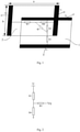
- a glass substrate is covered by two indium-tin oxide (ITO) transparent conductive layers (i.e., a first transparent conductive layer 1 and a second transparent conductive layer 2) serving as X electrode and Y electrode, respectively.
- ITO indium-tin oxide
- the two ITO transparent conductive layers are covered by a PET film.
- the two ITO transparent conductive layers are separated from each other, the lower ITO transparent conductive layer is attached to the glass substrate, and the upper ITO transparent conductive layer is attached to the PET film.
- Positive and negative terminals of the X electrode and positive and negative terminals of the Y electrode are respectively led out from two ends of the X electrode and two ends of the Y electrode by conductive bars (black bar-like portions in the Fig.1 ), and the conductive bar of the X electrode is perpendicular to the conductive bar of the Y electrode.
- the positive and negative terminals of the X electrode include a first voltage signal terminal X+ and a second voltage signal terminal X-
- the positive and negative terminals of the Y electrode includes a third voltage signal terminal Y+ and a fourth voltage signal terminal Y-, there are four connecting terminals, and that is how the four-wire resistive touch panel gets its name.
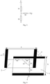
- an X coordinate of the touch point is calculated.
- a driving voltage U is applied to the third voltage signal terminal Y+, the fourth voltage signal terminal Y- is grounded, and the first voltage signal terminal X+ is served as a leading terminal to measure a voltage Vx of the touch point.
- the ITO transparent conductive layer is homogeneously conductive.
- a Y coordinate of the touch point is calculated.
- a driving voltage U is applied to the first voltage signal terminal X+, the second voltage signal terminal X- is grounded, and the third voltage signal terminal Y+ is served as a leading terminal to measure a voltage Vy of the touch point.
- the ITO transparent conductive layer is homogeneously conductive.
- the inventor founds that at least following issues are existed in the related art: it can be seen from the equivalent circuit diagrams ( Fig.2 and Fig.3 ) that, the first voltage signal terminal X+ is served as one leading terminal to measure the voltage Vx of the touch point when calculating the X coordinate of the touch point, and the third voltage signal terminal Y+ is served as one leading terminal to measure the voltage Vy of the touch point when calculating the Y coordinate of the touch point.
- V x R 4 R 3 + R 4 U
- V y R 2 R 1 + R 2 U .
- Document US2009/0128512 A1 discloses a secured touch screen device which comprises a resistive touch screen having a plurality of touch positions, having a first pair of first and second terminals at opposite ends of a first axis of the touch screen, and a second pair of first and second terminals at opposite ends of a second axis of the touch screen, the second axis being orthogonal to the first axis.
- the invention is set out in the appended set of claims.
- the present disclosure is to provide a touch panel with high touch sensitivity and a method for determining a touch point and a display device in order to solve the issues in the touch panel of the related art.
- a technical scheme to solve the issues presented by the present disclosure is to provide a touch panel, including a first transparent conductive layer and a second transparent conductive layer opposite to and away from each other; a first voltage signal terminal and a second voltage signal terminal opposite to the first voltage signal terminal are arranged on the first transparent conductive layer, a third voltage signal terminal and a fourth voltage signal terminal opposite to the third voltage signal terminal are arranged on the second transparent conductive layer, and an extension direction of the first voltage signal terminal is perpendicular to an extension direction of the third voltage signal terminal.
- the second voltage signal terminal and the fourth voltage signal terminal are short-circuited.
- the touch display panel further includes a voltage output unit, a read unit and a calculation unit.
- the voltage output unit is configured to input a driving voltage to the first voltage signal terminal and the third voltage signal terminal alternately and input a low voltage to the second voltage signal terminal and the fourth voltage signal terminal which are short-circuited based on a control signal.
- the read unit is configured to read a voltage value of the third voltage signal terminal when inputting the driving voltage to the first voltage signal terminal and read a voltage value of the first voltage signal terminal when inputting the driving voltage to the third voltage signal terminal.
- the calculation unit is configured to calculate a coordinate value of a touch point based on the read voltage value of the third voltage signal terminal and the read voltage value of the first voltage signal terminal.
- the touch panel further includes a control unit configured to generate the control signal to control a voltage output of the voltage output unit.
- the voltage output unit inputs a low voltage of 0V to the second voltage signal terminal and the fourth voltage signal terminal which are short-circuited.
- R1 is resistance between the touch point and the first voltage signal terminal
- R2 is resistance between the touch point and the second voltage signal terminal
- R3 is resistance between the touch point and the third voltage signal terminal
- R4 is resistance between the touch point and the fourth voltage signal terminal
- R 1 +R 2 R x
- R 3 +R 4 R Y
- R ⁇ R 2 .
- a is a horizontal distance between the third voltage signal terminal and the fourth voltage signal terminal on the touch panel
- b is a vertical distance between the first voltage signal terminal and the second voltage signal terminal on the touch panel
- Vx is the read voltage value of the first voltage signal terminal
- Vy is the read voltage value of the third voltage signal terminal.
- the method includes: inputting a driving voltage to the first voltage signal terminal and the third voltage signal terminal alternately, and inputting simultaneously a low voltage to the second voltage signal terminal and the fourth voltage signal terminal which are short-circuited; reading a voltage value of the third voltage signal terminal when inputting the driving voltage to the first voltage signal terminal, and reading a voltage value of the first voltage signal terminal when inputting the driving voltage to the third voltage signal terminal; and calculating a coordinate value of a touch point based on the read voltage value of the third voltage signal terminal and the read voltage value of the first voltage signal terminal.
- a step of inputting the driving voltage to the first voltage signal terminal and the third voltage signal terminal alternately and inputting simultaneously the low voltage to the second voltage signal terminal and the fourth voltage signal terminal which are short-circuited includes: under a control of a control signal, inputting the driving voltage to the first voltage signal terminal and the third voltage signal terminal alternately and inputting simultaneously the low voltage to the second voltage signal terminal and the fourth voltage signal terminal which are short-circuited.
- a low voltage of 0V is input to the second voltage signal terminal and the fourth voltage signal terminal which are short-circuited.
- R 4 R 2 + R 4 ; a is a horizontal distance between the third voltage signal terminal and the fourth voltage signal terminal on the touch panel; b is a vertical distance between the first voltage signal terminal and the second voltage signal terminal on the touch panel; Vx is the read voltage value of the first voltage signal terminal; and Vy is the read voltage value of the third voltage signal terminal.
- Yet another technical scheme to solve the issues presented by the present disclosure is to provide a display device including the above touch panel.
- the location (coordinate) of the touch point may be determined more accurately by the method for determining the touch point on the touch panel according to the present disclosure.
- the display device according to the present disclosure has better performance due to the touch panel hereinabove.
- a touch panel is provided in the present disclosure.
- the touch panel includes a first transparent conductive layer 1 and a second transparent conductive layer 2 opposite to and away from each other.
- a first voltage signal terminal X+ and a second voltage signal terminal X- opposite to the first voltage signal terminal X+ are arranged on the first transparent conductive layer 1.
- a third voltage signal terminal Y+ and a fourth voltage signal terminal Y- opposite to the third voltage signal terminal Y+ are arranged on the second transparent conductive layer 2.
- An extension direction of the first voltage signal terminal X+ is perpendicular to an extension direction of the third voltage signal terminal Y+.
- the second voltage signal terminal X- and the fourth voltage signal terminal Y- are short-circuited.
- the touch display panel further includes a voltage output unit, a read unit and a calculation unit.
- the voltage output unit is configured to, according to a control signal, alternately input a driving voltage to the first voltage signal terminal X+ and the third voltage signal terminal Y+ and input a low voltage to the second voltage signal terminal X- and the fourth voltage signal terminal Y-which are short-circuited.
- the read unit is configured to read a voltage value of the third voltage signal terminal Y+ when inputting the driving voltage to the first voltage signal terminal X+ and read a voltage value of the first voltage signal terminal X+ when inputting the driving voltage to the third voltage signal terminal Y+.
- the calculation unit is configured to calculate a coordinate value of a touch point based on a read voltage value of the third voltage signal terminal Y+ and a read voltage value of the first voltage signal terminal X+.
- the driving voltage provided by the voltage output unit is U
- the low voltage is 0V
- resistance RT at the touch point is very small and thereby it is ignored.
- the voltage Vx measured according to the embodiment of the present disclosure may be of a smaller error and have a higher accuracy.
- the resistance of R ⁇ is also smaller than that of R2, therefore the voltage Vy measured according to the embodiment of the present disclosure may be more accurate than the Vy measured according to the related art.
- the second voltage signal terminal X- and the fourth voltage signal terminal Y- are shorted, resistors between the touch point and a low voltage terminal are connected in parallel, thus an equivalent resistance between the touch point and the low voltage terminal is reduced, thereby a big size resistive touch panel may be equivalent to a small size resistive touch panel, and low sensitivity of the big size resistive touch panel is solved.
- the touch panel further includes a control unit configured to generate the control signal to control a voltage output of the voltage output unit.
- the control signal generated by the control unit may control the voltage output unit to output the driving voltage to the third voltage signal terminal Y+ at a first time point and simultaneously output a low voltage to the second voltage signal terminal X- and the fourth voltage signal terminal Y- mutually shorted, thereby measuring and obtaining the voltage Vx of the first voltage signal terminal X+.
- the control signal generated by the control unit may control the voltage output unit to output the driving voltage to the first voltage signal terminal X+ at a second time point and simultaneously output the low voltage to the second voltage signal terminal X- and the fourth voltage signal terminal Y- which are short-circuited, thereby measuring and obtaining the voltage Vy of the third voltage signal terminal Y+.
- a location (coordinates) of the touch point may be determined based on the obtained Vx and Vy.
- the voltage output unit may output a low voltage of 0V to the second voltage signal terminal X- and the fourth voltage signal terminal Y- which are short-circuited.
- the output voltage may be any voltage lower than the driving voltage.
- R1 is resistance between the touch point and the first voltage signal terminal X+
- R2 is resistance between the touch point and the second voltage signal terminal X-
- R3 is resistance between the touch point and the third voltage signal terminal Y+
- R4 is resistance between the touch point and the fourth voltage signal terminal Y-.
- R 4 R 2 + R 4 a is a horizontal distance between the third voltage signal terminal Y+ and the fourth voltage signal terminal Y- on the touch panel, b is a vertical distance between the first voltage signal terminal X+ and the second voltage signal terminal X- on the touch panel, Vx is a read voltage value of the first voltage signal terminal X+, and Vy is read voltage value of the third voltage signal terminal Y+.
- R 1 UV y ⁇ 2 V x V y R X + UV x R Y V x ⁇ UV y ⁇ 2 V x V y R X + UV x R Y V x 2 ⁇ 4 V y V x V y ⁇ U 2 V x U ⁇ V y R X R Y U ⁇ V y 2 V y V x V y ⁇ U 2 V x U ⁇ V y
- ⁇ X a ⁇ aV y U ⁇ V x R Y V x U ⁇ V y • UV y ⁇ 2 V x V y R X + UV x R Y V x ⁇ UV y ⁇ 2 V x V y R X + UV x R Y V x 2 ⁇ 4 V y V x V y ⁇ U 2 V
- the resistance RT at the touch point is very small and thereby it is ignored, on the basis of this, the second voltage signal terminal X- and the fourth voltage signal terminal Y- are shorted, to connect in parallel resistors between the touch point and the low voltage terminal so as to reduce the resistance between the touch point and the low voltage terminal, thereby improving the accuracy of voltage measurement and the sensitivity of the touch panel.
- a method for determining a touch point on a touch panel is provided in the embodiment.
- the touch panel is the touch panel according to the embodiment 1.
- the method includes: inputting a driving voltage to the first voltage signal terminal X+ and the third voltage signal terminal Y+ alternately, and inputting simultaneously a low voltage to the second voltage signal terminal X- and the fourth voltage signal terminal Y- which are short-circuited; reading a voltage value of the third voltage signal terminal Y+ when inputting the driving voltage to the first voltage signal terminal X+, and reading a voltage value of the first voltage signal terminal X+ when inputting the driving voltage to the third voltage signal terminal Y+; and calculating a coordinate value of a touch point based on the read voltage value of the third voltage signal terminal Y+ and the read voltage value of the first voltage signal terminal X+.
- a step of inputting the driving voltage to the first voltage signal terminal X+ and the third voltage signal terminal Y+ alternately and inputting simultaneously the low voltage to the second voltage signal terminal X- and the fourth voltage signal terminal Y-which are short-circuited includes: under a control of a control signal, inputting the driving voltage to the first voltage signal terminal X+ and the third voltage signal terminal Y+ alternately and inputting simultaneously the low voltage to the second voltage signal terminal X- and the fourth voltage signal terminal Y- which are short-circuited.
- a low voltage of 0V is input to the second voltage signal terminal X- and the fourth voltage signal terminal Y- which are short-circuited.
- R1 is resistance between the touch point and the first voltage signal terminal X+;
- R2 is resistance between the touch point and the second voltage signal terminal X-;
- R3 is resistance between the touch point and the third voltage signal terminal Y+;
- R4 is resistance between the touch point and the fourth voltage signal terminal Y-;
- R 1 +R 2 R x ;
- R 3 +R 4 R Y ;
- R ⁇ R 2 .
- the touch panel is the touch panel according to the embodiment 1, so a touched location (coordinate) on the touch panel is determined accurately by the method for determining the location (coordinate) of the touch point on the touch panel provided by the embodiment 2.
- a display device is provided in the embodiment 3, including the touch panel according to the embodiment 1, so the display device according to the embodiment 3 is of high sensitivity.
- the display device may be a product or a component with display function such as cell phone, tablet PC, television, display, laptop, digital photo frame and navigator.
- the display device may further include other normal structure such as a display driving unit.
Claims (5)
- Berührungstafel, umfassend:1.1 eine erste transparente leitfähige Schicht (1) und eine zweite transparente leitfähige Schicht (2), die einander gegenüberliegen und voneinander beabstandet sind;1.2 wobei ein erster Spannungssignalanschluss (X+) und ein zweiter Spannungssignalanschluss (X-), der dem ersten Spannungssignalanschluss (X+) gegenüber liegt, auf der ersten transparenten leitfähigen Schicht (1) angeordnet sind,1.3 wobei ein dritter Spannungssignalanschluss (Y+) und ein vierter Spannungssignalanschluss (Y-), der dem dritten Spannungssignalanschluss (Y+) gegenüber liegt, auf der zweiten transparenten leitfähigen Schicht (2) angeordnet sind,1.4 und eine Erstreckungsrichtung des ersten Spannungssignalanschlusses (X+) senkrecht zu einer Erstreckungsrichtung des dritten Spannungssignalanschlusses (Y+) verläuft;1.5 wobei die Berührungsanzeigetafel umfasst:
eine Leseeinheit, die dafür ist, einen Spannungswert des dritten Spannungssignalanschlusses (Y+) zu lesen, wenn die Treiberspannung an den ersten Spannungssignalanschluss (X+) angelegt wird, und einen Spannungswert des ersten Spannungssignalanschlusses (X+) zu lesen, wenn die Treiberspannung an den dritten Spannungssignalanschluss (Y+) angelegt wird; und1.6 eine Berechnungseinheit, die dafür eingerichtet ist, einen Koordinatenwert eines Berührungspunktes auf der Grundlage des gelesenen Spannungswertes des dritten Spannungssignalanschlusses (Y+) und des gelesenen Spannungswertes des ersten Spannungssignalanschlusses (X+) zu berechnen, dadurch gekennzeichnet, dass1.7 der zweite Spannungssignalanschluss (X-) und der vierte Spannungssignalanschluss (Y-) kurzgeschlossen sind und dass1.8 die Berührungsanzeigetafel eine Spannungsausgabeeinheit umfasst, die dafür eingerichtet ist, auf der Grundlage eines Steuersignals abwechselnd eine Treiberspannung an den ersten Spannungssignalanschluss (X+) und den dritten Spannungssignalanschluss (Y+) anzulegen und eine niedrige Spannung an den zweiten Spannungssignalanschluss (X-) und den vierten Spannungssignalanschluss (Y-), die kurzgeschlossen sind, anzulegen;wobei die Spannungsausgabeeinheit mit dem ersten Spannungssignalanschluss (X+) und dem dritten Spannungssignalanschluss (Y+) verbunden ist und mit dem zweiten Spannungssignalanschluss (X-) und dem vierten Spannungssignalanschluss (Y-), die kurzgeschlossen sind, verbunden ist;die Berührungstafel eine Steuereinheit umfasst, die dafür eingerichtet ist, das Steuersignal zu generieren, um eine Spannungsausgabe der Spannungsausgabeeinheit zu steuern; wobei die Spannungsausgabeeinheit eine niedrige Spannung von 0 V an den zweiten Spannungssignalanschluss (X-) und den vierten Spannungssignalanschluss (Y-), die kurzgeschlossen sind, anlegt;wobei die Berechnungseinheit den Koordinatenwert (X, Y) des Berührungspunktes auf der Grundlage der folgenden Formel berechnet: wobei R1 der Widerstand zwischen dem Berührungspunkt und dem ersten Spannungssignalanschluss (X+) ist;R2 der Widerstand zwischen dem Berührungspunkt und dem zweiten Spannungssignalanschluss (X-) ist;R3 der Widerstand zwischen dem Berührungspunkt und dem dritten Spannungssignalanschluss (Y+) ist;R4 der Widerstand zwischen dem Berührungspunkt und dem vierten Spannungssignalanschluss (Y-) ist;

 a eine horizontale Distanz zwischen dem dritten Spannungssignalanschluss (Y+) und dem vierten Spannungssignalanschluss (Y-) an der Berührungstafel ist;b eine vertikale Distanz zwischen dem ersten Spannungssignalanschluss (X+) und dem zweiten Spannungssignalanschluss (X-) an der Berührungstafel ist;Vx der gelesene Spannungswert des ersten Spannungssignalanschlusses (X+) ist;Vy der gelesene Spannungswert des dritten Spannungssignalanschlusses (Y+) ist; undU die Treiberspannung ist;wobei der erste Spannungssignalanschluss (X+), der dritte Spannungssignalanschluss (Y+), der zweite Spannungssignalanschluss (X-) und der vierte Spannungssignalanschluss (Y-) jeweils mit verschiedenen Ausgangsanschlüssen der Spannungsausgabeeinheit verbunden sind.
 - Berührungsbildschirm nach Anspruch 1, wobei der Berührungsbildschirm eine Steuereinheit umfasst, die dafür eingerichtet ist, das Steuersignal zu generieren, um eine Spannungsausgabe der Spannungsausgabeeinheit zu.
- Verfahren zum Bestimmen eines Berührungspunktes auf der Berührungstafel nach Anspruch 1, wobei das Verfahren umfasst:Anlegen einer Treiberspannung abwechselnd an den ersten Spannungssignalanschluss (X+) und den dritten Spannungssignalanschluss (Y+) und gleichzeitiges Anlegen einer niedrigen Spannung an den zweiten Spannungssignalanschluss (X-) und den vierten Spannungssignalanschluss (Y-), die kurzgeschlossen sind;Lesen eines Spannungswertes des dritten Spannungssignalanschlusses (Y+), wenn die Treiberspannung an den ersten Spannungssignalanschluss (X+) angelegt wird, und Lesen eines Spannungswertes des ersten Spannungssignalanschlusses (X+), wenn die Treiberspannung an den dritten Spannungssignalanschluss (Y+) angelegt wird; undBerechnen eines Koordinatenwertes eines Berührungspunktes auf der Grundlage des gelesenen Spannungswertes des dritten Spannungssignalanschlusses (Y+) und des gelesenen Spannungswertes des ersten Spannungssignalanschlusses (X+) ;wobei eine niedrige Spannung von 0 V an den zweiten Spannungssignalanschluss (X-) und den vierten Spannungssignalanschluss (Y-), die kurzgeschlossen sind, anlegt wird;wobei der Koordinatenwert des Berührungspunktes auf der Grundlage der folgenden Formel berechnet wird:
 wobei R1 der Widerstand zwischen dem Berührungspunkt und dem ersten Spannungssignalanschluss (X+) ist;R2 der Widerstand zwischen dem Berührungspunkt und dem zweiten Spannungssignalanschluss (X-) ist;R3 der Widerstand zwischen dem Berührungspunkt und dem dritten Spannungssignalanschluss (Y+) ist;R4 der Widerstand zwischen dem Berührungspunkt und dem vierten Spannungssignalanschluss (Y-) ist;

 a eine horizontale Distanz zwischen dem dritten Spannungssignalanschluss (Y+) und dem vierten Spannungssignalanschluss (Y-) an der Berührungstafel ist;b eine vertikale Distanz zwischen dem ersten Spannungssignalanschluss (X+) und dem zweiten Spannungssignalanschluss (X-) an der Berührungstafel ist;Vx der gelesene Spannungswert des ersten Spannungssignalanschlusses (X+) ist;Vy der gelesene Spannungswert des dritten Spannungssignalanschlusses (Y+) ist; undU die Treiberspannung ist; undwobei der erste Spannungssignalanschluss (X+), der dritte Spannungssignalanschluss (Y+), der zweite Spannungssignalanschluss (X-) und der vierte Spannungssignalanschluss (Y-) jeweils mit verschiedenen Ausgangsanschlüssen einer Spannungsausgabeeinheit verbunden sind.
 - Verfahren nach Anspruch 3, wobei der Schritt des Anlegens der Treiberspannung abwechselnd an den ersten Spannungssignalanschluss (X+) und den dritten Spannungssignalanschluss (Y+) und des gleichzeitigen Anlegens der niedrigen Spannung an den zweiten Spannungssignalanschluss (X-) und den vierten Spannungssignalanschluss (Y-) die kurzgeschlossen sind, umfasst:
unter einer Steuerung eines Steuersignals, Anlegen einer Treiberspannung abwechselnd an den ersten Spannungssignalanschluss (X+) und den dritten Spannungssignalanschluss (Y+) und gleichzeitiges Anlegen einer niedrigen Spannung an den zweiten Spannungssignalanschluss (X-) und den vierten Spannungssignalanschluss (Y-), die kurzgeschlossen sind. - Anzeigevorrichtung, umfassend die Berührungstafel nach Anspruch 1.
Applications Claiming Priority (2)
| Application Number | Priority Date | Filing Date | Title |
|---|---|---|---|
| CN201410494398.9A CN104298415B (zh) | 2014-09-24 | 2014-09-24 | 触控面板及触控点的确定方法、显示装置 |
| PCT/CN2015/070110 WO2016045244A1 (zh) | 2014-09-24 | 2015-01-05 | 触控面板及触控点的确定方法、显示装置 |
Publications (3)
| Publication Number | Publication Date |
|---|---|
| EP3200055A1 EP3200055A1 (de) | 2017-08-02 |
| EP3200055A4 EP3200055A4 (de) | 2018-05-09 |
| EP3200055B1 true EP3200055B1 (de) | 2022-03-16 |
Family
ID=52318167
Family Applications (1)
| Application Number | Title | Priority Date | Filing Date |
|---|---|---|---|
| EP15753300.1A Active EP3200055B1 (de) | 2014-09-24 | 2015-01-05 | Berührungssteuerungstafel, bestimmungsverfahren für berührungspunkt und anzeigevorrichtung |
Country Status (4)
| Country | Link |
|---|---|
| US (1) | US9632620B2 (de) |
| EP (1) | EP3200055B1 (de) |
| CN (1) | CN104298415B (de) |
| WO (1) | WO2016045244A1 (de) |
Families Citing this family (1)
| Publication number | Priority date | Publication date | Assignee | Title |
|---|---|---|---|---|
| CN109069931A (zh) * | 2017-05-31 | 2018-12-21 | 深圳市大疆创新科技有限公司 | 装甲板、装甲板上射击点的位置检测方法、装置及机器人 |
Family Cites Families (12)
| Publication number | Priority date | Publication date | Assignee | Title |
|---|---|---|---|---|
| WO2001061634A2 (en) * | 2000-02-15 | 2001-08-23 | Siemens Technology-To-Business Center, Llc | Tactile sensor |
| US8144130B2 (en) * | 2007-11-20 | 2012-03-27 | I-Pos Systems, Llc | Secured touch screen |
| CN101452129B (zh) * | 2007-12-05 | 2010-12-08 | 群康科技(深圳)有限公司 | 触摸屏和触摸屏显示装置 |
| CN101464768B (zh) * | 2007-12-20 | 2011-02-16 | 宸鸿光电科技股份有限公司 | 触控装置的触控感测方法 |
| CN101271374B (zh) * | 2008-05-19 | 2011-02-16 | 北京中星微电子有限公司 | 一种对触摸屏进行检测的方法及装置 |
| EP2204726A1 (de) * | 2008-12-30 | 2010-07-07 | STMicroelectronics R&D Oy | Steuerung mit Berührungsbildschirm |
| JP5029767B2 (ja) * | 2010-04-27 | 2012-09-19 | カシオ計算機株式会社 | 抵抗膜式タッチパネルの接触状態検出方法、タッチパネル装置、及び表示装置 |
| JP2012014683A (ja) * | 2010-06-03 | 2012-01-19 | Panasonic Corp | 入力装置 |
| CN103218103B (zh) * | 2012-01-18 | 2016-06-22 | 范钦雄 | 四线式电阻式触控面板的两点触控方法 |
| CN102981688B (zh) | 2012-11-19 | 2016-06-15 | 深圳市新国都技术股份有限公司 | 一种五线电阻屏控制电路 |
| CN203350858U (zh) | 2013-05-15 | 2013-12-18 | 东莞市奥思睿德世浦电子科技有限公司 | 一种四线电阻屏的新型组合结构 |
| CN103412699B (zh) * | 2013-06-28 | 2017-02-15 | 北京君正集成电路股份有限公司 | 一种四线电阻触摸屏两点触控手势识别的方法 |
-
2014
- 2014-09-24 CN CN201410494398.9A patent/CN104298415B/zh active Active
-
2015
- 2015-01-05 US US14/771,656 patent/US9632620B2/en active Active
- 2015-01-05 WO PCT/CN2015/070110 patent/WO2016045244A1/zh active Application Filing
- 2015-01-05 EP EP15753300.1A patent/EP3200055B1/de active Active
Also Published As
| Publication number | Publication date |
|---|---|
| CN104298415A (zh) | 2015-01-21 |
| WO2016045244A1 (zh) | 2016-03-31 |
| EP3200055A1 (de) | 2017-08-02 |
| US20160364064A1 (en) | 2016-12-15 |
| US9632620B2 (en) | 2017-04-25 |
| EP3200055A4 (de) | 2018-05-09 |
| CN104298415B (zh) | 2017-02-15 |
Similar Documents
| Publication | Publication Date | Title |
|---|---|---|
| CN105975137B (zh) | 一种触控显示面板及触控显示装置 | |
| KR101452660B1 (ko) | 터치 스크린 렌더링 시스템 및 그 동작 방법 | |
| US8432373B2 (en) | Patterned resistive touch panel | |
| US8487906B2 (en) | Method for detecting a touched position on a touch device | |
| US20110279410A1 (en) | Touch screen input apparatus | |
| US20150097805A1 (en) | Touch screen film, and touch screen using said film, and stylus pen used together with said film | |
| EP3327559A1 (de) | Berührungsdruckempfindlichkeitskorrekturverfahren und computerlesbares aufzeichnungsmedium | |
| US8803841B2 (en) | Touch spot detecting method of touch panel | |
| CN101714046A (zh) | 物体位置检测装置与方法及应用该装置的图像显示系统 | |
| JP5426429B2 (ja) | 入力装置及びそれを備えた表示装置 | |
| KR101405164B1 (ko) | 터치 디스플레이 장치 | |
| CN107368218B (zh) | 一种阵列基板、触控显示面板及其显示装置 | |
| WO2018003660A1 (ja) | 位置検出方法、位置検出装置及び位置検出プログラム | |
| EP3200055B1 (de) | Berührungssteuerungstafel, bestimmungsverfahren für berührungspunkt und anzeigevorrichtung | |
| US8730205B2 (en) | Touch panel input device and gesture detecting method | |
| JP5628885B2 (ja) | 感圧シートの押圧状態検出方法と感圧シート | |
| JP2007207124A (ja) | 座標検出装置、表示装置および座標検出方法 | |
| CN107291299B (zh) | 一种阵列基板、触控显示面板及其显示装置 | |
| JP6612983B2 (ja) | 位置検出装置 | |
| US9785300B2 (en) | Touch detection method and device | |
| JP4879388B2 (ja) | タブレット装置 | |
| Calpe et al. | AD7879 Controller Enables Gesture Recognition on Resistive Touch Screens | |
| JP2019159446A (ja) | 位置検出装置 | |
| CN103455231A (zh) | 触摸屏的触摸位置获得方法、装置以及接触电压获得方法 | |
| JP2013041521A (ja) | 座標検出装置 |
Legal Events
| Date | Code | Title | Description |
|---|---|---|---|
| PUAI | Public reference made under article 153(3) epc to a published international application that has entered the european phase |
Free format text: ORIGINAL CODE: 0009012 |
|
| STAA | Information on the status of an ep patent application or granted ep patent |
Free format text: STATUS: REQUEST FOR EXAMINATION WAS MADE |
|
| 17P | Request for examination filed |
Effective date: 20150831 |
|
| AK | Designated contracting states |
Kind code of ref document: A1 Designated state(s): AL AT BE BG CH CY CZ DE DK EE ES FI FR GB GR HR HU IE IS IT LI LT LU LV MC MK MT NL NO PL PT RO RS SE SI SK SM TR |
|
| AX | Request for extension of the european patent |
Extension state: BA ME |
|
| DAX | Request for extension of the european patent (deleted) | ||
| A4 | Supplementary search report drawn up and despatched |
Effective date: 20180409 |
|
| RIC1 | Information provided on ipc code assigned before grant |
Ipc: G06F 3/041 20060101ALI20180403BHEP Ipc: G06F 3/045 20060101AFI20180403BHEP |
|
| STAA | Information on the status of an ep patent application or granted ep patent |
Free format text: STATUS: EXAMINATION IS IN PROGRESS |
|
| 17Q | First examination report despatched |
Effective date: 20200605 |
|
| STAA | Information on the status of an ep patent application or granted ep patent |
Free format text: STATUS: EXAMINATION IS IN PROGRESS |
|
| GRAP | Despatch of communication of intention to grant a patent |
Free format text: ORIGINAL CODE: EPIDOSNIGR1 |
|
| STAA | Information on the status of an ep patent application or granted ep patent |
Free format text: STATUS: GRANT OF PATENT IS INTENDED |
|
| INTG | Intention to grant announced |
Effective date: 20211129 |
|
| GRAS | Grant fee paid |
Free format text: ORIGINAL CODE: EPIDOSNIGR3 |
|
| GRAA | (expected) grant |
Free format text: ORIGINAL CODE: 0009210 |
|
| STAA | Information on the status of an ep patent application or granted ep patent |
Free format text: STATUS: THE PATENT HAS BEEN GRANTED |
|
| AK | Designated contracting states |
Kind code of ref document: B1 Designated state(s): AL AT BE BG CH CY CZ DE DK EE ES FI FR GB GR HR HU IE IS IT LI LT LU LV MC MK MT NL NO PL PT RO RS SE SI SK SM TR |
|
| REG | Reference to a national code |
Ref country code: GB Ref legal event code: FG4D |
|
| REG | Reference to a national code |
Ref country code: CH Ref legal event code: EP |
|
| REG | Reference to a national code |
Ref country code: DE Ref legal event code: R096 Ref document number: 602015077568 Country of ref document: DE |
|
| REG | Reference to a national code |
Ref country code: IE Ref legal event code: FG4D |
|
| REG | Reference to a national code |
Ref country code: AT Ref legal event code: REF Ref document number: 1476359 Country of ref document: AT Kind code of ref document: T Effective date: 20220415 |
|
| REG | Reference to a national code |
Ref country code: LT Ref legal event code: MG9D |
|
| REG | Reference to a national code |
Ref country code: NL Ref legal event code: MP Effective date: 20220316 |
|
| PG25 | Lapsed in a contracting state [announced via postgrant information from national office to epo] |
Ref country code: SE Free format text: LAPSE BECAUSE OF FAILURE TO SUBMIT A TRANSLATION OF THE DESCRIPTION OR TO PAY THE FEE WITHIN THE PRESCRIBED TIME-LIMIT Effective date: 20220316 Ref country code: RS Free format text: LAPSE BECAUSE OF FAILURE TO SUBMIT A TRANSLATION OF THE DESCRIPTION OR TO PAY THE FEE WITHIN THE PRESCRIBED TIME-LIMIT Effective date: 20220316 Ref country code: NO Free format text: LAPSE BECAUSE OF FAILURE TO SUBMIT A TRANSLATION OF THE DESCRIPTION OR TO PAY THE FEE WITHIN THE PRESCRIBED TIME-LIMIT Effective date: 20220616 Ref country code: LT Free format text: LAPSE BECAUSE OF FAILURE TO SUBMIT A TRANSLATION OF THE DESCRIPTION OR TO PAY THE FEE WITHIN THE PRESCRIBED TIME-LIMIT Effective date: 20220316 Ref country code: HR Free format text: LAPSE BECAUSE OF FAILURE TO SUBMIT A TRANSLATION OF THE DESCRIPTION OR TO PAY THE FEE WITHIN THE PRESCRIBED TIME-LIMIT Effective date: 20220316 Ref country code: BG Free format text: LAPSE BECAUSE OF FAILURE TO SUBMIT A TRANSLATION OF THE DESCRIPTION OR TO PAY THE FEE WITHIN THE PRESCRIBED TIME-LIMIT Effective date: 20220616 |
|
| REG | Reference to a national code |
Ref country code: AT Ref legal event code: MK05 Ref document number: 1476359 Country of ref document: AT Kind code of ref document: T Effective date: 20220316 |
|
| PG25 | Lapsed in a contracting state [announced via postgrant information from national office to epo] |
Ref country code: LV Free format text: LAPSE BECAUSE OF FAILURE TO SUBMIT A TRANSLATION OF THE DESCRIPTION OR TO PAY THE FEE WITHIN THE PRESCRIBED TIME-LIMIT Effective date: 20220316 Ref country code: GR Free format text: LAPSE BECAUSE OF FAILURE TO SUBMIT A TRANSLATION OF THE DESCRIPTION OR TO PAY THE FEE WITHIN THE PRESCRIBED TIME-LIMIT Effective date: 20220617 Ref country code: FI Free format text: LAPSE BECAUSE OF FAILURE TO SUBMIT A TRANSLATION OF THE DESCRIPTION OR TO PAY THE FEE WITHIN THE PRESCRIBED TIME-LIMIT Effective date: 20220316 |
|
| PG25 | Lapsed in a contracting state [announced via postgrant information from national office to epo] |
Ref country code: NL Free format text: LAPSE BECAUSE OF FAILURE TO SUBMIT A TRANSLATION OF THE DESCRIPTION OR TO PAY THE FEE WITHIN THE PRESCRIBED TIME-LIMIT Effective date: 20220316 |
|
| PG25 | Lapsed in a contracting state [announced via postgrant information from national office to epo] |
Ref country code: SM Free format text: LAPSE BECAUSE OF FAILURE TO SUBMIT A TRANSLATION OF THE DESCRIPTION OR TO PAY THE FEE WITHIN THE PRESCRIBED TIME-LIMIT Effective date: 20220316 Ref country code: SK Free format text: LAPSE BECAUSE OF FAILURE TO SUBMIT A TRANSLATION OF THE DESCRIPTION OR TO PAY THE FEE WITHIN THE PRESCRIBED TIME-LIMIT Effective date: 20220316 Ref country code: RO Free format text: LAPSE BECAUSE OF FAILURE TO SUBMIT A TRANSLATION OF THE DESCRIPTION OR TO PAY THE FEE WITHIN THE PRESCRIBED TIME-LIMIT Effective date: 20220316 Ref country code: PT Free format text: LAPSE BECAUSE OF FAILURE TO SUBMIT A TRANSLATION OF THE DESCRIPTION OR TO PAY THE FEE WITHIN THE PRESCRIBED TIME-LIMIT Effective date: 20220718 Ref country code: ES Free format text: LAPSE BECAUSE OF FAILURE TO SUBMIT A TRANSLATION OF THE DESCRIPTION OR TO PAY THE FEE WITHIN THE PRESCRIBED TIME-LIMIT Effective date: 20220316 Ref country code: EE Free format text: LAPSE BECAUSE OF FAILURE TO SUBMIT A TRANSLATION OF THE DESCRIPTION OR TO PAY THE FEE WITHIN THE PRESCRIBED TIME-LIMIT Effective date: 20220316 Ref country code: CZ Free format text: LAPSE BECAUSE OF FAILURE TO SUBMIT A TRANSLATION OF THE DESCRIPTION OR TO PAY THE FEE WITHIN THE PRESCRIBED TIME-LIMIT Effective date: 20220316 Ref country code: AT Free format text: LAPSE BECAUSE OF FAILURE TO SUBMIT A TRANSLATION OF THE DESCRIPTION OR TO PAY THE FEE WITHIN THE PRESCRIBED TIME-LIMIT Effective date: 20220316 |
|
| PG25 | Lapsed in a contracting state [announced via postgrant information from national office to epo] |
Ref country code: PL Free format text: LAPSE BECAUSE OF FAILURE TO SUBMIT A TRANSLATION OF THE DESCRIPTION OR TO PAY THE FEE WITHIN THE PRESCRIBED TIME-LIMIT Effective date: 20220316 Ref country code: IS Free format text: LAPSE BECAUSE OF FAILURE TO SUBMIT A TRANSLATION OF THE DESCRIPTION OR TO PAY THE FEE WITHIN THE PRESCRIBED TIME-LIMIT Effective date: 20220716 Ref country code: AL Free format text: LAPSE BECAUSE OF FAILURE TO SUBMIT A TRANSLATION OF THE DESCRIPTION OR TO PAY THE FEE WITHIN THE PRESCRIBED TIME-LIMIT Effective date: 20220316 |
|
| REG | Reference to a national code |
Ref country code: DE Ref legal event code: R097 Ref document number: 602015077568 Country of ref document: DE |
|
| PLBE | No opposition filed within time limit |
Free format text: ORIGINAL CODE: 0009261 |
|
| STAA | Information on the status of an ep patent application or granted ep patent |
Free format text: STATUS: NO OPPOSITION FILED WITHIN TIME LIMIT |
|
| PG25 | Lapsed in a contracting state [announced via postgrant information from national office to epo] |
Ref country code: DK Free format text: LAPSE BECAUSE OF FAILURE TO SUBMIT A TRANSLATION OF THE DESCRIPTION OR TO PAY THE FEE WITHIN THE PRESCRIBED TIME-LIMIT Effective date: 20220316 |
|
| 26N | No opposition filed |
Effective date: 20221219 |
|
| PG25 | Lapsed in a contracting state [announced via postgrant information from national office to epo] |
Ref country code: SI Free format text: LAPSE BECAUSE OF FAILURE TO SUBMIT A TRANSLATION OF THE DESCRIPTION OR TO PAY THE FEE WITHIN THE PRESCRIBED TIME-LIMIT Effective date: 20220316 |
|
| PG25 | Lapsed in a contracting state [announced via postgrant information from national office to epo] |
Ref country code: IT Free format text: LAPSE BECAUSE OF FAILURE TO SUBMIT A TRANSLATION OF THE DESCRIPTION OR TO PAY THE FEE WITHIN THE PRESCRIBED TIME-LIMIT Effective date: 20220316 |
|
| REG | Reference to a national code |
Ref country code: DE Ref legal event code: R119 Ref document number: 602015077568 Country of ref document: DE |
|
| REG | Reference to a national code |
Ref country code: CH Ref legal event code: PL |
|
| GBPC | Gb: european patent ceased through non-payment of renewal fee |
Effective date: 20230105 |
|
| PG25 | Lapsed in a contracting state [announced via postgrant information from national office to epo] |
Ref country code: LU Free format text: LAPSE BECAUSE OF NON-PAYMENT OF DUE FEES Effective date: 20230105 |
|
| REG | Reference to a national code |
Ref country code: BE Ref legal event code: MM Effective date: 20230131 |
|
| PG25 | Lapsed in a contracting state [announced via postgrant information from national office to epo] |
Ref country code: LI Free format text: LAPSE BECAUSE OF NON-PAYMENT OF DUE FEES Effective date: 20230131 Ref country code: GB Free format text: LAPSE BECAUSE OF NON-PAYMENT OF DUE FEES Effective date: 20230105 Ref country code: DE Free format text: LAPSE BECAUSE OF NON-PAYMENT OF DUE FEES Effective date: 20230801 Ref country code: CH Free format text: LAPSE BECAUSE OF NON-PAYMENT OF DUE FEES Effective date: 20230131 |
|
| PG25 | Lapsed in a contracting state [announced via postgrant information from national office to epo] |
Ref country code: FR Free format text: LAPSE BECAUSE OF NON-PAYMENT OF DUE FEES Effective date: 20230131 Ref country code: BE Free format text: LAPSE BECAUSE OF NON-PAYMENT OF DUE FEES Effective date: 20230131 |
|
| PG25 | Lapsed in a contracting state [announced via postgrant information from national office to epo] |
Ref country code: IE Free format text: LAPSE BECAUSE OF NON-PAYMENT OF DUE FEES Effective date: 20230105 |