EP3190634A1 - Light emitting diode chip having distributed bragg reflector - Google Patents
Light emitting diode chip having distributed bragg reflector Download PDFInfo
- Publication number
- EP3190634A1 EP3190634A1 EP17153368.0A EP17153368A EP3190634A1 EP 3190634 A1 EP3190634 A1 EP 3190634A1 EP 17153368 A EP17153368 A EP 17153368A EP 3190634 A1 EP3190634 A1 EP 3190634A1
- Authority
- EP
- European Patent Office
- Prior art keywords
- light emitting
- bragg reflector
- distributed bragg
- emitting diode
- light
- Prior art date
- Legal status (The legal status is an assumption and is not a legal conclusion. Google has not performed a legal analysis and makes no representation as to the accuracy of the status listed.)
- Granted
Links
Images





Classifications
-
- H—ELECTRICITY
- H10—SEMICONDUCTOR DEVICES; ELECTRIC SOLID-STATE DEVICES NOT OTHERWISE PROVIDED FOR
- H10H—INORGANIC LIGHT-EMITTING SEMICONDUCTOR DEVICES HAVING POTENTIAL BARRIERS
- H10H20/00—Individual inorganic light-emitting semiconductor devices having potential barriers, e.g. light-emitting diodes [LED]
- H10H20/80—Constructional details
- H10H20/85—Packages
-
- H—ELECTRICITY
- H10—SEMICONDUCTOR DEVICES; ELECTRIC SOLID-STATE DEVICES NOT OTHERWISE PROVIDED FOR
- H10H—INORGANIC LIGHT-EMITTING SEMICONDUCTOR DEVICES HAVING POTENTIAL BARRIERS
- H10H20/00—Individual inorganic light-emitting semiconductor devices having potential barriers, e.g. light-emitting diodes [LED]
- H10H20/80—Constructional details
- H10H20/84—Coatings, e.g. passivation layers or antireflective coatings
- H10H20/841—Reflective coatings, e.g. dielectric Bragg reflectors
-
- H—ELECTRICITY
- H10—SEMICONDUCTOR DEVICES; ELECTRIC SOLID-STATE DEVICES NOT OTHERWISE PROVIDED FOR
- H10H—INORGANIC LIGHT-EMITTING SEMICONDUCTOR DEVICES HAVING POTENTIAL BARRIERS
- H10H20/00—Individual inorganic light-emitting semiconductor devices having potential barriers, e.g. light-emitting diodes [LED]
- H10H20/80—Constructional details
- H10H20/81—Bodies
- H10H20/814—Bodies having reflecting means, e.g. semiconductor Bragg reflectors
-
- H—ELECTRICITY
- H10—SEMICONDUCTOR DEVICES; ELECTRIC SOLID-STATE DEVICES NOT OTHERWISE PROVIDED FOR
- H10H—INORGANIC LIGHT-EMITTING SEMICONDUCTOR DEVICES HAVING POTENTIAL BARRIERS
- H10H20/00—Individual inorganic light-emitting semiconductor devices having potential barriers, e.g. light-emitting diodes [LED]
- H10H20/80—Constructional details
- H10H20/85—Packages
- H10H20/855—Optical field-shaping means, e.g. lenses
- H10H20/856—Reflecting means
-
- H—ELECTRICITY
- H10—SEMICONDUCTOR DEVICES; ELECTRIC SOLID-STATE DEVICES NOT OTHERWISE PROVIDED FOR
- H10H—INORGANIC LIGHT-EMITTING SEMICONDUCTOR DEVICES HAVING POTENTIAL BARRIERS
- H10H20/00—Individual inorganic light-emitting semiconductor devices having potential barriers, e.g. light-emitting diodes [LED]
- H10H20/01—Manufacture or treatment
- H10H20/011—Manufacture or treatment of bodies, e.g. forming semiconductor layers
- H10H20/018—Bonding of wafers
-
- H—ELECTRICITY
- H10—SEMICONDUCTOR DEVICES; ELECTRIC SOLID-STATE DEVICES NOT OTHERWISE PROVIDED FOR
- H10W—GENERIC PACKAGES, INTERCONNECTIONS, CONNECTORS OR OTHER CONSTRUCTIONAL DETAILS OF DEVICES COVERED BY CLASS H10
- H10W90/00—Package configurations
- H10W90/701—Package configurations characterised by the relative positions of pads or connectors relative to package parts
- H10W90/751—Package configurations characterised by the relative positions of pads or connectors relative to package parts of bond wires
- H10W90/756—Package configurations characterised by the relative positions of pads or connectors relative to package parts of bond wires between a chip and a stacked lead frame, conducting package substrate or heat sink
Definitions
- the present disclosure relates to a light emitting diode chip, a method of fabricating the same, and a light emitting diode package, and more particularly, to a light emitting diode chip having a distributed Bragg reflector, a method of fabricating the same, and a light emitting diode package having a distributed Bragg reflector.
- a gallium nitride-based light emitting diode chip emitting blue or ultraviolet rays has been used for various applications.
- various types of light emitting diode packages emitting mixed color light for example, white light required for a backlight unit, general lighting, or the like, have been marketed.
- the light output from the light emitting diode package mainly depends on the light efficiency of the light emitting diode chip
- research to improve the light efficiency of the light emitting diode chip have been continuously conducted.
- attempts to improve the light extraction efficiency of the light emitting diode chip have been continuously performed.
- a technology of forming a metal reflector or a distributed Bragg reflector on a bottom surface of a transparent substrate such as a sapphire has been known as one of the attempts.
- FIG. 1 shows reflectivity measured by forming an aluminum layer on the bottom surface of the sapphire substrate in the related art.
- FIG. 2 shows the reflectivity measured by the distributed Bragg reflector formed by periodically applying TiO 2 /SiO 2 to the bottom surface of the sapphire substrate in the related art.
- DBR distributed Bragg reflector
- the DBR can only increase the reflectivity for a part of the visible range. Therefore, the reflectivity for other ranges is considerably low. That is, as shown in FIG. 2 , the reflectivity for a wavelength of about 520 nm or more is suddenly reduced while most of the reflectivity is less than 50% at a wavelength of 550 nm or more.
- the DBR shows high reflectivity for light of the blue wavelength range emitted from the light emitting diode chip but the DBR does not show efficient reflection characteristics for light of the green and/or red wavelength range. Therefore, there is a limit in improving the light efficiency in the package.
- the present invention provides a light emitting diode chip capable of increasing light efficiency of a light emitting diode package implementing a mixed color light, for example, white light.
- the present invention also provides a light emitting diode package capable of improving light efficiency.
- the present invention also provides a distributed Bragg reflector having high reflectivity over a wide wavelength range, a light emitting diode chip having the same, and a light emitting diode package.
- a light emitting diode chip having a distributed Bragg reflector includes a substrate, a light emitting structure which is positioned on a upper portion of the substrate and includes an active layer interposed between a first conductive-type semiconductor layer and a second conductive-type semiconductor layer, and a distributed Bragg reflector that reflects light emitted from the light emitting structure.
- the distributed Bragg reflector has a reflectivity of 90% or more for light of a first wavelength in a blue wavelength range, light of a second wavelength in a green wavelength range, and light of a third wavelength in a red wavelength range.
- the distributed Bragg reflector when the light emitting diode chip is applied to a light emitting diode package implementing mixed color light, for example, white light, blue light, green light, and red light can be effectively reflected, thereby making it possible to improve the light efficiency of the light emitting diode package.
- mixed color light for example, white light, blue light, green light, and red light
- the distributed Bragg reflector may be positioned on a lower portion of the substrate.
- the distributed Bragg reflector may be positioned on the lower surface of the substrate to contact the lower surface of the substrate.
- the lower surface of the substrate may have a surface roughness of 3 ⁇ m or less.
- the upper surface of the substrate may include a predetermined pattern.
- the substrate may be a patterned sapphire substrate.
- the area of the substrate may be 90,000 ⁇ m 2 or more.
- the area of the substrate may be 300 ⁇ 300 ⁇ m 2 or more or 1 ⁇ 1 mm 2 or more.
- the present invention is very advantageous in the light emitting diode chip having a relatively larger area by the distributed Bragg reflector formed over a wide area.
- the light emitting diode chip may include a plurality of light emitting cells formed on the substrate. Further, the light emitting diode chip may include at least one light emitting cell array in which the plurality of light emitting cells are connected in series.
- the distributed Bragg reflector may include a first distributed Bragg reflector and a second distributed Bragg reflector.
- the first distributed Bragg reflector may have higher reflectivity for light of the blue wavelength range than for light of the red wavelength range and the second distributed Bragg reflector may have higher reflectivity for light of the green wavelength range or the red wavelength range than for light of the blue wavelength range.
- the position of the distributed Bragg reflector is not specially limited.
- the distributed Bragg reflector may be positioned on the lower portion of the substrate.
- the first distributed Bragg reflector may be positioned to be closer to the substrate than the second distributed Bragg reflector.
- the distributed Bragg reflector may be positioned between the substrate and the light emitting structure. In this case, the first distributed Bragg reflector may be positioned to be closer to the light emitting structure than the second distributed Bragg reflector.
- the distributed Bragg reflector may include a plurality of pairs of first material layer having a first optical thickness and second material layer having a second optical thickness and a plurality of pairs of third material layers having a third optical thickness and fourth material layers having a fourth optical thickness.
- the refractive index of the first material layer is different from the refractive index of the second material layer and the refractive index of the third material layer is different from the refractive index of the fourth material layer.
- the plurality of pairs of first material layer and second material layer may be positioned to be closer to the light emitting structure than the plurality of pairs of third material layers and fourth material layers.
- the first material layer and the second material layer each have the same refractive index as the third material layer and the fourth material layer.
- the first optical thickness may be thinner than the third optical thickness and the second optical thickness may be thinner than the fourth optical thickness.
- the plurality of pairs of first material layers and second material layers may be mixed with the plurality of pairs of third material layer and fourth material layer.
- first optical thickness and the second optical thickness may satisfy the relationship of the integer multiple.
- third optical thickness and the fourth optical thickness may satisfy the relationship of the integer multiple.
- first optical thickness and the second optical thickness may be the same as each other and the third optical thickness and the fourth optical thickness may be the same as each other.
- the present invention also discloses a light emitting diode package having a distributed Bragg reflector.
- the light emitting diode package includes a mounting surface on which a light emitting diode chip is mounted, a light emitting diode chip which is mounted on the mounting surface, and a reflecting surface that reflects at least a part of the light emitted from the light emitting diode chip.
- the distributed Bragg reflector having reflectivity of 90% or more for light of a first wavelength in a blue wavelength range, light of a second wavelength in a green wavelength range, and light of a third wavelength in a red wavelength range is positioned on at least a part of the reflecting surface.
- the distributed Bragg reflector may be formed using, for example, an ion assisted deposition techniques.
- the present invention also discloses a light emitting diode chip having a distributed Bragg reflector.
- the light emitting diode chip includes a substrate having a front surface and a rear surface, a light emitting structure which is positioned on the front surface of the substrate and includes an active layer interposed between a first conductive-type semiconductor layer and a second conductive-type semiconductor layer; and a distributed Bragg reflector that is positioned on the rear surface of the substrate and reflecting light emitted from the light emitting structure.
- the surface roughness of the rear surface of the substrate has an RMS value of 3 nm or less and the distributed Bragg reflector has a reflectivity of 90% or more for light of a first wavelength in a blue wavelength range, light of a second wavelength in a green wavelength range, and light of a third wavelength in a red wavelength range.
- the surface roughness of the rear surface of the substrate may have an RMS value of 2 nm or less, preferably, 1 nm or less.
- the reflectivity of the distributed Bragg reflector is improved according to the surface roughness.
- the distributed Bragg reflector when the light emitting diode chip is applied to a light emitting diode package implementing mixed color light, for example, white light, blue light, green light, and red light can be effectively reflected, thereby making it possible to improve light efficiency of the light emitting diode package.
- mixed color light for example, white light, blue light, green light, and red light
- the distributed Bragg reflector may be positioned on the rear surface of the substrate to contact the rear surface of the substrate.
- the front surface of the substrate may include a pattern.
- the substrate may be a patterned sapphire substrate.
- the area of the substrate may be 90,000 ⁇ m 2 or more.
- the area of the substrate may be 300 ⁇ 300 ⁇ m 2 or more or 1 ⁇ 1 mm 2 or more.
- the present invention is very advantageous in the light emitting diode chip having a relatively larger area by the distributed Bragg reflector formed over a wide area.
- the light emitting diode chip may include a plurality of light emitting cells formed on the front surface of the substrate. Further, the light emitting diode chip may include at least one light emitting cell array in which the plurality of light emitting cells are connected in series.
- the distributed Bragg reflector may include a first distributed Bragg reflector and a second distributed Bragg reflector.
- the first distributed Bragg reflector may have higher reflectivity for light of the blue wavelength range than for light of the red wavelength range and the second distributed Bragg reflector may have higher reflectivity for light of the green wavelength range or the red wavelength range than for light of the blue wavelength range.
- first distributed Bragg reflector may be positioned to be closer to the substrate than the second distributed Bragg reflector.
- the distributed Bragg reflector may include a plurality of pairs of first material layer having a first optical thickness and second material layer having a second optical thickness and a plurality of pairs of third material layers having a third optical thickness and fourth material layers having a fourth optical thickness.
- the refractive index of the first material layer is different from the refractive index of the second material layer and the refractive index of the third material layer is different from the refractive index of the fourth material layer.
- the plurality of pairs of first material layers and second material layers may be positioned to be closer to the light emitting structure than the plurality of pairs of third material layer and fourth material layer.
- the first material layer and the second material layer each have the same refractive index as the third material layer and the fourth material layer.
- the first optical thickness may be thinner than the third optical thickness and the second optical thickness may be thinner than the fourth optical thickness.
- the plurality of pairs of first material layer and second material layer may be mixed with the plurality of pairs of third material layer and fourth material layer.
- first optical thickness and the second optical thickness may satisfy the relationship of the integer multiple.
- third optical thickness and the fourth optical thickness may satisfy the relationship of the integer multiple.
- first optical thickness and the second optical thickness may be the same as each other and the third optical thickness and the fourth optical thickness may be the same as each other.
- the present invention also discloses a method of fabricating a light emitting diode chip having a distributed Bragg reflector.
- the method includes forming a light emitting structure on a front surface of a substrate.
- the light emitting structure includes a first conductive-type semiconductor layer, a second conductive-type semiconductor layer, and an active layer interposed between the first conductive-type semiconductor layer and the second conductive-type semiconductor layer.
- a part of the substrate is removed by grinding a rear surface of the substrate, and after the grinding, a surface roughness of the rear surface of the substrate is reduced by lapping the substrate.
- the distributed Bragg reflector is formed on the rear surface of the substrate.
- the surface roughness of the rear surface of the substrate has an RMS value of 3 nm or less before forming the distributed Bragg reflector.
- the distributed Bragg reflector has a reflectivity of 90% or more for light of a first wavelength in a blue wavelength range, light of a second wavelength in a green wavelength range, and light of a third wavelength in a red wavelength range.
- the surface roughness of the rear surface of the substrate may have an RMS value of 1 nm or less before forming the distributed Bragg reflector.
- the method may further include polishing the rear surface of the substrate by a chemical mechanical polishing process after performing the lapping.
- the rear surface of the substrate may be polished by the chemical mechanical polishing process so that the surface roughness of the rear surface of the substrate has an RMS value of 1 nm or less.
- a reflective metal layer or a protective layer may be formed on the distributed Bragg reflector.
- the reflective metal layer or the protective layer protects the distributed Bragg reflector when the light emitting diode chip is mounted on the light emitting diode package.
- the distributed Bragg reflector may be formed using, for example, an ion assisted deposition techniques.
- a distributed Bragg reflector which has a higher reflectivity over a wide wavelength range of visible light, is provided, and thus, light efficiency of a light emitting diode package implementing mixed color light, for example, white light, can be improved. Further, employing a technique to form the distributed Bragg reflector on a light emitting diode package without damaging the package, a light emitting diode package with an improved light efficiency can be provided.
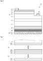
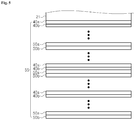
- FIG. 3 is a cross-sectional view for explaining a light emitting diode chip 20 having the distributed Bragg reflector 45 according to an exemplary embodiment of the present invention and FIG. 4 is a magnified cross-sectional view of the distributed Bragg reflector 45 of FIG. 3 .
- a light emitting diode chip 20 includes a substrate 21, a light emitting structure 30, and a distributed Bragg reflector 45.
- the light emitting diode chip 20 may include a buffer layer 23, a transparent electrode 31, a p-electrode pad 33, an n-electrode pad 35, a reflective metal layer 51, and a protective layer 53.
- the substrate 21 is a transparent substrate, for example, a sapphire or a SiC substrate, but not specifically limited thereto.
- An upper surface, i.e., front surface of the substrate 21 may have a predetermined pattern, such as a patterned sapphire substrate PSS. Meanwhile, an area of the substrate 21 determines the entire chip area.
- the area of the substrate 21 is preferably 90,000 ⁇ m 2 or more, more preferably, 1 mm 2 or more.
- a light emitting structure 30 is positioned on the upper portion of the substrate 21.
- the light emitting structure 30 includes a first conductive-type semiconductor layer 25, a second conductive-type semiconductor layer 29, and an active layer 27 interposed between the first and second conductive-type semiconductor layers 25 and 29.
- the first conductive-type layer and the second conductive-type layer have a conductive type opposite to each other, wherein the first conductive type is an n-type and the second conductive type may be a p-type, or vice versa.
- the first conductive-type semiconductor layer 25, the active layer 27, and the second conductive-type semiconductor layer 29 may be made of a gallium nitride-based compound semiconductor material, that is, (Al, In, Ga)N.
- the constituent elements and composition of the active layer 27 are determined to emit light of a required wavelength, for example, ultraviolet rays or blue light.
- the first conductive-type semiconductor layer 25 and/or the second conductive-type semiconductor layer 29 may be formed in a single layer structure as shown or a multi-layer structure.
- the active layer 27 may be formed to be a single quantum well structure or a multi quantum well structure.
- a buffer layer 23 may be interposed between the substrate 21 and the first conductive-type semiconductor layer 25.
- the semiconductor layers 25, 27, and 29 may be formed using a MOCVD technology or a MBE technology and a region of the first conductive-type semiconductor layer 25 may be patterned to be partially exposed using a photolithography and etching process.
- the transparent electrode layer 31 may be formed of, for example, ITO or Ni/Au, on the second conductive-type semiconductor layer 29.
- the transparent electrode layer 31 serves to spread current due to a lower specific resistance than the second conductive-type semiconductor layer 29.
- a p-electrode pad 33 is formed on the transparent electrode layer 31 and an n-electrode pad 35 is formed on the first conductive-type semiconductor layer 25. As shown, the p-electrode pad 33 may be contacted to the second conductive-type semiconductor layer 29 through the transparent electrode layer 31.
- the distributed Bragg reflector 45 is positioned on the lower portion, i.e., rear surface of the substrate 21.
- the distributed Bragg reflector 45 may include a first distributed Bragg reflector 40 and a second distributed Bragg reflector 50.
- the first distributed Bragg reflector 40 is formed by repeating a plurality of pairs of first material layers 40a and second material layers 40b and the second distributed Bragg reflector 50 is formed by repeating a plurality of pairs of third material layers 50a and fourth material layers 50b.
- the plurality of pairs of first material layer 40a and second material layer 40b have relatively higher reflectivity for light of a red wavelength range, for example, 550 nm or 630 nm, than for light of a blue wavelength range and the second distributed Bragg reflector 50 may have relatively higher reflectivity for light of a blue wavelength range, for example, light of 460 nm than for light of a red or green wavelength range.
- the optical thickness of the material layers 40a and 40b within the first distributed Bragg reflector 40 is thicker than the optical thickness of the material layers 50a and 50b within the second distributed Bragg reflector 50, or vice versa, without being limited thereto.
- the first material layer 40a may be the same material as the third material layer 50a, that is, the same refractive index and the second material layer 40b may be the same material as the fourth material layer 50b, that is, the same refractive index.
- the first material layer 40a and the third material layer 50a may be made of TiO 2 (n: about 2.5) and the second material layer 40b and the fourth material layer 50b may be made of SiO 2 (n: about 1.5).
- the optical thickness (refractive index ⁇ thickness) of the first material layer 40a may substantially have the relationship of an integer multiple with the optical thickness of the second material layer 40b and the optical thicknesses thereof may be substantially the same as each other.
- the optical thickness of the third material layer 50a may substantially have the relationship of an integer multiple with the optical thickness of the fourth material layer 50b and the optical thicknesses thereof may be substantially the same as each other.
- the optical thickness of the first material layer 40a may be thicker than that of the third material layer 50a and the optical thickness of the second material layer 40b may be thicker than that of the fourth material layer 50b.
- the optical thickness of the first to fourth material layers 40a, 40b, 50a, and 50b may be controlled by controlling the refractive index and/or real thickness of each material layer.
- the reflective meta layer 51 of Al, Ag, or Rh, or the like may be formed on the lower portion of the distributed Bragg reflector 45 and a protective layer 53 for protecting the distributed Bragg reflector 45 may be formed thereon.
- the protective layer 53 may be made of any one metal layer of, for example, Ti, Cr, Ni, Pt, Ta, and Au or an alloy thereof.
- the protective layer 53 protects the distributed Bragg reflector 45 from external impact or pollution.
- the reflective metal layer 51 or the protective layer 53 prevents the distributed Bragg reflector 45 from being deformed from a material such as an adhesive when the light emitting diode chip is mounted in the light emitting diode package.
- the distributed Bragg reflector 45 including the first distributed Bragg reflector 40 having high reflectivity for visible light of a relatively long wavelength and the second distributed Bragg reflector 50 having high reflectivity for visible light of a relatively short wavelength, which have a mutually stacked structure, is provided.
- the distributed Bragg reflector 45 may increase the reflectivity for light over most of the visible range by a combination of the first distributed Bragg reflector 40 and the second distributed Bragg reflector 50.
- the distributed Bragg reflector according to the related art has high reflectivity for light of a specific wavelength range but has relatively low reflectivity for light of a different wavelength range, such that there is a limit in improving the light efficiency in the light emitting diode package emitting white light.
- the distributed Bragg reflector 45 may have high reflectivity for light of the blue wavelength range as well as high reflectivity for light of the green wavelength range and light of the red wavelength range, thereby making it possible to improve light efficiency of the light emitting diode package.
- the light loss in the distributed Bragg reflector 45 may be further reduced in the case where the first distributed Bragg reflector 40 is disposed to be closer to the substrate than the second distributed Bragg reflector 50.
- the exemplary embodiment describes two reflectors, i.e., the first distributed Bragg reflector 40 and the second distributed Bragg reflector 50, more reflectors may be used. In this case, the reflectors having relatively higher reflectivity for a long wavelength may be positioned to be relatively closer to the light emitting structure 30. However, the exemplary embodiment is not limited thereto.
- the thicknesses of the first material layers 40a within the first distributed Bragg reflector 40 may be different from each other. Further, the thicknesses of the second material layers 40b may be different from each other. In addition, the thicknesses of the thirdt material layers 50a within the second distributed Bragg reflector 50 may be different from each other. Further, the thicknesses of the fourth material layers 50b may be different from each other.
- the distributed Bragg reflector 45 may be disposed on the lower portion of the substrate 21, the distributed Bragg reflector 45 may be disposed between the substrate 21 and the light emitting structure 30.
- the first distributed Bragg reflector 40 may be disposed to be closer to the light emitting structure 30 than the second distributed Bragg reflector 50.
- the material layers 40a, 40b, 50a, and 50b are made of SiO 2 or TiO 2 , but is not limited thereto. Therefore, they may be made of, other material layers, for example, Si 3 N 4 , compound semiconductor, or the like. However, it is preferable that the difference in the refractive indexes between the first material layer 40a and the second material layer 40b and the difference in the refractive indexes between the third material layer 50a and the fourth material layer 50b are each larger than 0.5.
- the total number of pairs may be 10 or more, preferably, 20 or more.
- the surface roughness of the rear surface of the substrate 21 may be controlled to have an RMS value of 3 nm or less.
- the surface roughness of the rear surface of the substrate 21 may have an RMS value of 2 nm or less, preferably, an RMS value of 1 nm or less.
- the surface roughness of the substrate 21 is controlled before forming the distributed Bragg reflector 45.
- the rear surface of the substrate 21 with the light emitting structures formed thereon is primarily ground to remove a part of the substrate 21, thereby thinning the substrate 21.
- the rear surface of the substrate 21 is scratched by the grinding, such that it is relatively very rough.
- the surface of the substrate 21 is lapped using slurry having small particles. In the lapping process, the depth of the groove such as the scratch in the surface of the substrate 21, etc., is reduced, thereby reducing the surface roughness.
- the surface roughness of the rear surface of the substrate 21 may be controlled to be 3um or less by controlling a particle size of diamond slurry and a surface plate used in the lapping process. Thereafter, the surface of the substrate 21 may be additionally treated by chemicals. Generally, it is difficult to control the surface roughness using only the lapping process using the surface plate and the slurry particle. Therefore, after reducing the surface roughness by the lapping process, the rear surface of the substrate 21 may be polished by a chemical mechanical polishing process. The surface roughness of the rear surface of the substrate 21 may be controlled up to 1 nm or less by the CMP process.
- the material layers having different refractive indexes such as TiO 2 , SiO 2 , and Si 3 N 4 , or the like are repeatedly deposited on the surface of the substrate 21.
- the deposition of the material layers may be made by various methods such as sputtering, electron beam deposition, plasma enhanced chemical vapor deposition method, etc.
- the ion assisted deposition method may be used.
- the ion assisted deposition method forms the material layers having a proper thickness by measuring the reflectivity of the material layer deposited on the substrate 21, such that it is suitable to form the material layers of the distributed Bragg reflector.
- the metal layer may be formed on the distributed Bragg reflector. Thereafter, the substrate is diced, thereby completing the individual light emitting diode chips.
- FIG. 5 is a cross-sectional view for explaining a distributed Bragg reflector 55 according to another exemplary embodiment of the present invention.
- FIGS. 3 and 4 show and describe when the distributed Bragg reflector 45 has the stacked structure of the first distributed Bragg reflector 40 and the second distributed Bragg reflector 50.
- a plurality of pairs of first material layers 40a and second material layers 40b are mixed with a plurality of pairs of third material layers 50a and a fourth material layers 50b.
- at least one pair of the third material layer 50a and the fourth material layer 50b is positioned between the plurality of pairs of the first material layer 40a and the second material layer 40b.
- At least one pair of the first material layer 40a and the second material layer 40b is positioned between the plurality of pairs of the third material layer 50a and the fourth material layer 50b.
- the optical thickness of the first to fourth material layers 40a, 40b, 50a, and 50b is controlled to have high reflectivity for light over the wide visible range.
- the distributed Bragg reflector 55 may be positioned on the lower portion of the substrate 21 but is not limited thereto and may be positioned between the substrate 21 and the light emitting structure 30 (see FIG. 3 ).
- FIG. 6 is a graph showing reflectivity of a distributed Bragg reflector on the sapphire substrate according to an exemplary embodiment of the present invention.
- the distributed Bragg reflector has been formed using TiO 2 /SiO 2 .
- the distributed Bragg reflector was formed to have the stacked structure of the first distributed Bragg reflector 40 and the second distributed Bragg reflector 50. The reflectivity was measured over the entire wavelength range of the visible light and the same sample was measured seven times.
- the first distributed Bragg reflector 40 has a central wavelength of about 630 nm and the second distributed Bragg reflector 50 has a central wavelength of about 460 nm. As shown in FIG.
- the reflectivity of 90% or more, even 98% or more, for light of a blue wavelength range of 400 to 500 nm, light of a green wavelength range of 500 to 600 nm, and light of a red wavelength range of 600 to 700 nm may be obtained by employing the distributed Bragg reflector.
- the high reflectivity of 90% or more is obtained over the entire range of 400 to 700 nm as shown in FIG. 6 . Even in the case where the reflectivity less than 90% is obtained in a part of the intermediate range belongs to the present invention if the present invention has the distributed Bragg reflector having two or more central wavelengths.
- FIG. 7 is a cross sectional view for explaining a light emitting diode chip 20a having a plurality of light emitting cells according to another exemplary embodiment of the present invention.
- the light emitting diode chip 20a includes a plurality of light emitting cells on the substrate 21 and also includes the distributed Bragg reflector 45.
- the substrate 21 and the distributed Bragg reflector 45 is similar to the distributed Bragg reflector described with referenced to FIGS. 3 to 5 and therefore, the detailed description thereof will be omitted.
- the substrate 21 may be an insulator to electrically isolate the plurality of light emitting cells.
- the substrate 21 may be a patterned sapphire substrate.
- the plurality of light emitting cells 30 are positioned to be spaced apart from each other.
- Each of the plurality of light emitting cells 30 is the same as the light emitting structure 30 with reference to FIG. 3 and the detailed description thereof will be omitted.
- the buffer layers 23 may be interposed between the light emitting cells 30 and the substrate 21 and the buffer layers 23 may be also spaced apart from each other.
- the first insulating layer 37 covers the front surface of the light emitting cells 30.
- a first insulating layer 37 has openings on the first conductive-type semiconductor layers 25 and has openings on the second conductive-type semiconductor layers 29. The side walls of the light emitting cells 30 are covered by the first insulating layer 37.
- the first insulating layer 37 also covers the substrate 21 in the regions between the light emitting cells 30.
- the first insulating layer 37 may be formed of a silicon oxide (SiO 2 ) layer or a silicon nitride layer and may be a layer formed in a temperature range of 200 to 300C° using a plasma chemical vapor deposition method. In this case, the first insulating layer 37 may be formed to have a thickness of 4500 ⁇ to 1 ⁇ m.
- the first insulating layer When the first insulating layer is formed to have a thickness smaller than 4500 ⁇ , the first insulating layer having a relatively thin thickness is formed at the bottom sides of the light emitting cells due to step coverage characteristics and an electrical short circuit between the wirings and the light emitting cells formed on the first insulating layer may occur. Meanwhile, as the thickness of the first insulating layer becomes thick, the electrical short circuit may be prevented but light transmittance is deteriorated to reduce the luminous efficiency. Therefore, it is preferable that the first insulating layer is formed not to exceed a thickness of 1 ⁇ m.
- the wirings 39 are formed on the first insulating layer 37.
- the wirings 39 are electrically connected to the first conductive-type semiconductor layers 25 and the second conductive-type semiconductor layers 29 through the openings.
- the transparent electrode layers 31 may be disposed on the second conductive-type semiconductor layers 29 and the wirings may be connected to the transparent electrode layers 31.
- the wirings 29 electrically connect the first conductive-type semiconductor layers 25 to the second conductive-type semiconductors 29, respectively, of the adjacent light emitting cells 30, such that a serial array of the light emitting cells 30 may be formed.
- the arrays may be formed in plural and the plurality of arrays are connected to each other in anti-parallel so that they may be driven to be connected to an AC power supply.
- a bridge rectifier (not shown) connected to the serial arrays of the light emitting cells may be connected and the light emitting cells may be driven under the AC power supply by the bridge rectifier.
- the bridge rectifier may be formed by connecting the light emitting cells having the same structure as the light emitting cells 30 using the wirings 29.
- the wirings may connect the first conductive-type semiconductor layers 25 of the adjacent light emitting cells to each other or the second conductive-type semiconductor layer 29 to each other. Therefore, the plurality of light emitting cells 30 connected in series and parallel may be provided.
- the wirings 29 may be made of a conductive material, for example, doped semiconductor material such as polycrystalline silicon or metal.
- the wirings 29 may be formed in a multi structure and may include, for example, a lower layer of Cr or Ti and an upper layer of Cr or Ti. Further, the metal layer of Au, Au/Ni, or Au/Al may be interposed between the lower layer and the upper layer.
- the second insulating layer 41 may cover the wirings 39 and the first insulating layer 37.
- the second insulating layer 41 prevents the wirings 39 from being polluted from moisture, or the like and prevents the wirings 39 and the light emitting cells 30 from being damaged from external impact.
- the second insulating layer 41 may be formed of the same material as the first insulating layer 37 and the silicon oxide layer SiO 2 or the silicon nitride layer.
- the second insulating layer 41 may be a layer formed in the temperature range of 200 to 300°C by using the plasma chemical vapor deposition method, similar to the first insulating layer.
- the first insulating layer 37 is a layer formed by using the plasma chemical vapor deposition method
- the second insulating layer 41 may be a layer deposited in the temperature range of-20% to +20% for the deposition temperature of the first insulating layer 37, more preferably, a layer deposited in the same deposition temperature.
- the second insulating layer 41 has a relatively thin thickness as compared to the first insulating layer 37, preferably, a thickness of 500 ⁇ or more.
- the second insulating layer 41 is relatively thinner than the first insulating layer 37, which can prevent the second insulating layer from peeling off from the first insulating layer.
- the second insulating layer is thinner than 2500 ⁇ , it is difficult to protect the wiring and the light emitting cell from the external impact or the moisture permeation.
- a phosphor layer 43 may be positioned on the light emitting diode chip 20a.
- the phosphor layer 43 may be a layer in which resin is dispersed in a phosphor or a layer deposited by an electrophoresis method.
- the phosphor layer 43 covers the second insulating layer 41, thereby converting the wavelength of light emitted from the light emitting cells 30.
- FIG. 8 is a cross-sectional view showing a light emitting diode package mounted with the light emitting diode chip having the distributed Bragg reflector according to an exemplary embodiment of the present invention.
- the light emitting diode package includes a package body 60, leads 61a and 61b, light emitting diode chips 20 or 20a, and a molding part 63.
- the package body 60 may be made of plastic resin.
- the package body 60 has a mounting surface M for mounting the light emitting diode chip 20 and also has a reflecting surface R reflecting light emitted from the light emitting diode chip 20. Meanwhile, the light emitting diode chip 20 is mounted on the mounting surface M and is electrically connected to leads 61a and 61b through bonding wires.
- the light emitting diode chip 20 may have the distributed Bragg reflector 45 described with reference to FIGS. 3 and 4 or may have the distributed Bragg reflector 55 described with reference to FIG. 5 .
- the light emitting diode package emits the mixed color light, for example, white light.
- the light emitting diode package may include a phosphor for converting the wavelength of light emitted from the light emitting diode chip 20.
- the phosphor may be included in the molding part 63 but is not limited thereto.
- the light emitting diode chip 20 includes the distributed Bragg reflector 45 or 55, when the light wavelength-converted in the phosphor faces the mounting surface M through the light emitting diode chip 20, the light is reflected to have high reflectivity while being emitted to the outside by the wavelength-converted light or the distributed Bragg reflector 45 or 55. Therefore, the light emitting diode package having higher light efficiency may be provided as compared to the light emitting diode package according to the related art.
- the exemplary embodiment describes the package including the phosphor together with the light emitting diode chip 20 in order to implement white light
- the present invention is not limited thereto.
- Various packages capable of emitting white light are known and the light emitting diode chip may be applied to any package.
- the exemplary embodiment describes when the light emitting diode chip 20 is mounted, the light emitting diode chip 20a may be on the mounting surface M with reference to FIG. 7 .
- the light emitting diode chip 20a includes the phosphor layer 43, the phosphor in the molding part 63 may be omitted.
- FIG. 9 is a cross-sectional view for explaining the light emitting diode package having the distributed Bragg reflector according to another exemplary embodiment of the present invention.
- the light emitting diode package is similar to most of the light emitting diode package described with reference to FIG. 8 . However, there is a difference in that a distributed Bragg reflector 75 is formed on the reflecting surface M. In addition, in the exemplary embodiment, the light emitting diode chip 90 may not have the distributed Bragg reflector 45 or 55 described in FIGS. 4 or 5 .
- the distributed Bragg reflector 75 may include a first distributed Bragg reflector 70 and a second distributed Bragg reflector 80.
- the first distributed Bragg reflector 70 and the second distributed Bragg reflector 80 may each have the stacked structure of the same material layer as the first and second distributed Bragg reflectors 40 and 50 with reference to FIG. 4 . That is, the first distributed Bragg reflector 70 may be formed in the plurality of pairs of first material layer 70a and second material layer 70b and the second distributed Bragg reflector 80 may be formed in a plurality of pairs of third material layer 80a and fourth material layer 80b.
- These first to fourth material layers 70a, 70b, 80a, and 80b are the same as the first to fourth material layers 40a, 40b, 50a, and 50b described with reference to FIG. 4 and therefore, the detailed description thereof will be omitted.
- High reflectivity may be provided over the wide wavelength range of the visible range by the distributed Bragg reflector 75 and therefore, the light efficiency of the light emitting diode package is improved.
- the distributed Bragg reflector may be formed by mixing the plurality of pairs of first and second material layers 70a and 70b and a plurality of pairs of third and fourth material layers 80a and 80b, similar to one described with reference to FIG. 5 .
- the distributed Bragg reflector 75 may be formed using the ion assisted deposition method performed at a relatively low temperature. Therefore, the distributed Bragg reflector 75 may be formed without damaging the package body 60 of the plastic resin or the leads 61a and 61b. The distributed Bragg reflector 75 may be formed over the entire region other than the lead regions for bonding the wires.
- a light emitting diode chip 90 may include the distributed Bragg reflector like the light emitting diode chips 20 or 20a of FIG. 7 but is not limited thereto.
- the light emitting diode chip 90 may be the general light emitting diode chip according to the related art.
- the distributed Bragg reflector having reflectivity of 90% or more for the light of the blue wavelength range, the light of the green wavelength range, and the light of the red wavelength range is installed, thereby making it possible to the light emitting diode package with the improved light efficiency.
- the state of the substrate surface on which the distributed Bragg reflector is formed may have an effect on the reflectivity of the distributed Bragg reflector.
- the experimental example performed in order to confirm that the state of the substrate surface has an effect on the reflectivity of the distributed Bragg reflector may have an effect on the reflectivity of the distributed Bragg reflector.
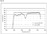
- FIG. 10 is a graph showing the reflectivity of the distributed Bragg reflector according to whether or not the CMP is performed after a sapphire substrate lapping process using a copper surface plate.
- the lapping process using the copper surface plate was performed by using the diamond slurry having a particle of 3 ⁇ m.
- the surface roughness of the rear surface of the sapphire substrate showed an RMS value of about 5.12 nm at an area of 5 ⁇ m ⁇ 5 ⁇ m.
- the above-mentioned first distributed Bragg reflector and second distributed Bragg reflector are formed by controlling the thickness of TiO 2 and SiO 2 to fabricate the sample (Example 1).
- the comparative example directly formed the distributed Bragg reflector similar to Example 1 without performing the chemical mechanical polishing process to fabricate the sample.
- the chemical mechanical polishing process was performed using slurry of SiO 2 at a load of 20 Kg and the surface roughness of the sapphire substrate showed the RMS value of about 0.25 nm at an area of 5 ⁇ m ⁇ 5 ⁇ m after the chemical mechanical polishing process.
- the reflectivity of the distributed Bragg reflector showed approximately 90% or more in the visible range as shown in FIG. 10 , but the reflectivity was irregular according to the wavelength and showed the value of 90% or less in the vicinity of 550 nm.
- most of the reflectivity of the distributed Bragg reflector showed a value close to 100% over the wide wavelength range of the visible rays.
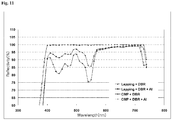
- FIG. 11 is a graph showing the reflectivity after an aluminum layer of about 500 nm is deposited on the sample fabricated in the same manner as the example and the comparative example of FIG. 10 .
- the comparative example it is considered as the phenomenon that the reduction in the reflectivity is showed after A1 was deposited since the distributed Bragg reflector according to the comparative example formed on the sapphire surface having a rough surface was deformed by the interfacial defect while the A1 was deposited using the electronic beam deposition technology.
- the surface roughness of the sapphire substrate is good, it is determined that reflectivity was maintained without deforming the distributed Bragg reflector while A1 is deposited.
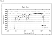
- FIGS. 12 to 14 are graphs showing the reflectivity of the distributed Bragg reflector according to a size of a slurry particle during the lapping process using a tin surface plate.
- the slurry included diamond particles and the size of the diamond particle was 3 ⁇ m, 4 ⁇ m, and 6 ⁇ m, respectively.
- the surface roughness of the sapphire substrate showed the RMS value of about 2.40nm, 3.35nm, and 4.18nm according to the size of the diamond particle after the lapping process was performed using a tin surface plate.
- Example 2 The same distributed Bragg reflector as Example 1 was formed after the lapping process was performed by the tin surface plate and A1 of 500 nm was deposited as in the example of FIG. 11 .
- the reflectivity of the distributed Bragg reflector was 90% or more over the wide wavelength range of the visible range after the lapping process was performed using the slurry of 3 ⁇ m and the tin surface plate. However, when the Al was deposited, the reflectivity was slightly reduced in the vicinity of 550 nm.
- the reflectivity of the distributed Bragg reflector does not reach 90% in the vicinity of 550 nm after the lapping process was performed using the slurry of 4 ⁇ m and the tin surface plate and the reflectivity was reduced to 80% or less after A1 was deposited.
- the surface roughness of the sapphire substrate has an effect on the reflectivity of the distributed Bragg reflector before the distributed Bragg reflector is formed.
- the surface roughness of the sapphire substrate is controlled to have the RMS value of 3nm or less, the reflectivity characteristics were considerably good.
- the surface roughness of the sapphire substrate is 1 nm or less, it is expected that the reflectivity would not be reduced even after A1 was deposited.
Landscapes
- Led Devices (AREA)
- Led Device Packages (AREA)
- Planar Illumination Modules (AREA)
Abstract
Description
- The present disclosure relates to a light emitting diode chip, a method of fabricating the same, and a light emitting diode package, and more particularly, to a light emitting diode chip having a distributed Bragg reflector, a method of fabricating the same, and a light emitting diode package having a distributed Bragg reflector.
- A gallium nitride-based light emitting diode chip emitting blue or ultraviolet rays has been used for various applications. In particular, various types of light emitting diode packages emitting mixed color light, for example, white light required for a backlight unit, general lighting, or the like, have been marketed.
- Since the light output from the light emitting diode package mainly depends on the light efficiency of the light emitting diode chip, research to improve the light efficiency of the light emitting diode chip have been continuously conducted. In particular, attempts to improve the light extraction efficiency of the light emitting diode chip have been continuously performed. A technology of forming a metal reflector or a distributed Bragg reflector on a bottom surface of a transparent substrate such as a sapphire has been known as one of the attempts.
-
FIG. 1 shows reflectivity measured by forming an aluminum layer on the bottom surface of the sapphire substrate in the related art. - It can be appreciated from
FIG. 1 that in the case of the sapphire substrate on which the aluminum layer is not formed, reflectivity of about 20% is shown, but in the case of the sapphire substrate on which the aluminum layer is formed, reflectivity of about 80% is shown over a wavelength of a visible range. -
FIG. 2 shows the reflectivity measured by the distributed Bragg reflector formed by periodically applying TiO2/SiO2 to the bottom surface of the sapphire substrate in the related art. - When the distributed Bragg reflector (DBR) is formed to reflect light from the light emitting diode chip, for example, light with a peak wavelength of 460 nm, instead of using the aluminum layer; it can be appreciated from
FIG. 2 that reflectivity reaches approximately 100% in a blue wavelength range, for example, a wavelength range of 400 to 500 nm. - However, the DBR can only increase the reflectivity for a part of the visible range. Therefore, the reflectivity for other ranges is considerably low. That is, as shown in
FIG. 2 , the reflectivity for a wavelength of about 520 nm or more is suddenly reduced while most of the reflectivity is less than 50% at a wavelength of 550 nm or more. - Therefore, when mounting the light emitting diode chip using the DBR in the light emitting diode package implementing white light, the DBR shows high reflectivity for light of the blue wavelength range emitted from the light emitting diode chip but the DBR does not show efficient reflection characteristics for light of the green and/or red wavelength range. Therefore, there is a limit in improving the light efficiency in the package.
- Meanwhile, attempts to apply the DBR to the reflecting surface of the light emitting diode package have been made, which are not achieved due to a limitation of the DBR deposition technology, for example, a problem in a deposition temperature, a plasma temperature, or the like.
- The present invention provides a light emitting diode chip capable of increasing light efficiency of a light emitting diode package implementing a mixed color light, for example, white light.
- The present invention also provides a light emitting diode package capable of improving light efficiency.
- The present invention also provides a distributed Bragg reflector having high reflectivity over a wide wavelength range, a light emitting diode chip having the same, and a light emitting diode package.
- Additional features of the invention will be set forth in the description which follows, and in part will be apparent from the description, or may be learned by practice of the invention.
- According to an aspect of the present invention, a light emitting diode chip having a distributed Bragg reflector is disclosed. The light emitting diode chip includes a substrate, a light emitting structure which is positioned on a upper portion of the substrate and includes an active layer interposed between a first conductive-type semiconductor layer and a second conductive-type semiconductor layer, and a distributed Bragg reflector that reflects light emitted from the light emitting structure. The distributed Bragg reflector has a reflectivity of 90% or more for light of a first wavelength in a blue wavelength range, light of a second wavelength in a green wavelength range, and light of a third wavelength in a red wavelength range.
- By employing the distributed Bragg reflector, when the light emitting diode chip is applied to a light emitting diode package implementing mixed color light, for example, white light, blue light, green light, and red light can be effectively reflected, thereby making it possible to improve the light efficiency of the light emitting diode package.
- The distributed Bragg reflector may be positioned on a lower portion of the substrate. In particular, the distributed Bragg reflector may be positioned on the lower surface of the substrate to contact the lower surface of the substrate. In this case, the lower surface of the substrate may have a surface roughness of 3 µm or less.
- In addition, the upper surface of the substrate may include a predetermined pattern. For example, the substrate may be a patterned sapphire substrate.
- Meanwhile, the area of the substrate may be 90,000 µm2 or more. For example, the area of the substrate may be 300×300 µm2 or more or 1×1 mm 2 or more. The present invention is very advantageous in the light emitting diode chip having a relatively larger area by the distributed Bragg reflector formed over a wide area.
- In addition, the light emitting diode chip may include a plurality of light emitting cells formed on the substrate. Further, the light emitting diode chip may include at least one light emitting cell array in which the plurality of light emitting cells are connected in series.
- In some exemplary embodiments, the distributed Bragg reflector may include a first distributed Bragg reflector and a second distributed Bragg reflector. For example, the first distributed Bragg reflector may have higher reflectivity for light of the blue wavelength range than for light of the red wavelength range and the second distributed Bragg reflector may have higher reflectivity for light of the green wavelength range or the red wavelength range than for light of the blue wavelength range.
- Further, the position of the distributed Bragg reflector is not specially limited. For example, the distributed Bragg reflector may be positioned on the lower portion of the substrate. In this case, the first distributed Bragg reflector may be positioned to be closer to the substrate than the second distributed Bragg reflector. Alternatively, the distributed Bragg reflector may be positioned between the substrate and the light emitting structure. In this case, the first distributed Bragg reflector may be positioned to be closer to the light emitting structure than the second distributed Bragg reflector.
- In some exemplary embodiments, the distributed Bragg reflector may include a plurality of pairs of first material layer having a first optical thickness and second material layer having a second optical thickness and a plurality of pairs of third material layers having a third optical thickness and fourth material layers having a fourth optical thickness. Herein, the refractive index of the first material layer is different from the refractive index of the second material layer and the refractive index of the third material layer is different from the refractive index of the fourth material layer.
- Further, the plurality of pairs of first material layer and second material layer may be positioned to be closer to the light emitting structure than the plurality of pairs of third material layers and fourth material layers. In addition, the first material layer and the second material layer each have the same refractive index as the third material layer and the fourth material layer. Further, the first optical thickness may be thinner than the third optical thickness and the second optical thickness may be thinner than the fourth optical thickness.
- In some exemplary embodiments, the plurality of pairs of first material layers and second material layers may be mixed with the plurality of pairs of third material layer and fourth material layer.
- Meanwhile, the first optical thickness and the second optical thickness may satisfy the relationship of the integer multiple. In addition, the third optical thickness and the fourth optical thickness may satisfy the relationship of the integer multiple. In particular, the first optical thickness and the second optical thickness may be the same as each other and the third optical thickness and the fourth optical thickness may be the same as each other.
- The present invention also discloses a light emitting diode package having a distributed Bragg reflector. The light emitting diode package includes a mounting surface on which a light emitting diode chip is mounted, a light emitting diode chip which is mounted on the mounting surface, and a reflecting surface that reflects at least a part of the light emitted from the light emitting diode chip. The distributed Bragg reflector having reflectivity of 90% or more for light of a first wavelength in a blue wavelength range, light of a second wavelength in a green wavelength range, and light of a third wavelength in a red wavelength range is positioned on at least a part of the reflecting surface.
- The distributed Bragg reflector may be formed using, for example, an ion assisted deposition techniques.
- The present invention also discloses a light emitting diode chip having a distributed Bragg reflector. The light emitting diode chip includes a substrate having a front surface and a rear surface, a light emitting structure which is positioned on the front surface of the substrate and includes an active layer interposed between a first conductive-type semiconductor layer and a second conductive-type semiconductor layer; and a distributed Bragg reflector that is positioned on the rear surface of the substrate and reflecting light emitted from the light emitting structure. Further, the surface roughness of the rear surface of the substrate has an RMS value of 3 nm or less and the distributed Bragg reflector has a reflectivity of 90% or more for light of a first wavelength in a blue wavelength range, light of a second wavelength in a green wavelength range, and light of a third wavelength in a red wavelength range.
- The surface roughness of the rear surface of the substrate may have an RMS value of 2 nm or less, preferably, 1 nm or less. The reflectivity of the distributed Bragg reflector is improved according to the surface roughness.
- Further, by employing the distributed Bragg reflector, when the light emitting diode chip is applied to a light emitting diode package implementing mixed color light, for example, white light, blue light, green light, and red light can be effectively reflected, thereby making it possible to improve light efficiency of the light emitting diode package.
- The distributed Bragg reflector may be positioned on the rear surface of the substrate to contact the rear surface of the substrate. In addition, the front surface of the substrate may include a pattern. For example, the substrate may be a patterned sapphire substrate.
- Meanwhile, the area of the substrate may be 90,000 µm2 or more. For example, the area of the substrate may be 300×300 µm2 or more or 1×1 mm2 or more. The present invention is very advantageous in the light emitting diode chip having a relatively larger area by the distributed Bragg reflector formed over a wide area.
- In addition, the light emitting diode chip may include a plurality of light emitting cells formed on the front surface of the substrate. Further, the light emitting diode chip may include at least one light emitting cell array in which the plurality of light emitting cells are connected in series.
- In some exemplary embodiments, the distributed Bragg reflector may include a first distributed Bragg reflector and a second distributed Bragg reflector. For example, the first distributed Bragg reflector may have higher reflectivity for light of the blue wavelength range than for light of the red wavelength range and the second distributed Bragg reflector may have higher reflectivity for light of the green wavelength range or the red wavelength range than for light of the blue wavelength range.
- In addition, the first distributed Bragg reflector may be positioned to be closer to the substrate than the second distributed Bragg reflector.
- In some exemplary embodiments, the distributed Bragg reflector may include a plurality of pairs of first material layer having a first optical thickness and second material layer having a second optical thickness and a plurality of pairs of third material layers having a third optical thickness and fourth material layers having a fourth optical thickness. Herein, the refractive index of the first material layer is different from the refractive index of the second material layer and the refractive index of the third material layer is different from the refractive index of the fourth material layer.
- Further, the plurality of pairs of first material layers and second material layers may be positioned to be closer to the light emitting structure than the plurality of pairs of third material layer and fourth material layer. In addition, the first material layer and the second material layer each have the same refractive index as the third material layer and the fourth material layer. Further, the first optical thickness may be thinner than the third optical thickness and the second optical thickness may be thinner than the fourth optical thickness.
- In some exemplary embodiments, the plurality of pairs of first material layer and second material layer may be mixed with the plurality of pairs of third material layer and fourth material layer.
- Meanwhile, the first optical thickness and the second optical thickness may satisfy the relationship of the integer multiple. In addition, the third optical thickness and the fourth optical thickness may satisfy the relationship of the integer multiple. In particular, the first optical thickness and the second optical thickness may be the same as each other and the third optical thickness and the fourth optical thickness may be the same as each other.
- The present invention also discloses a method of fabricating a light emitting diode chip having a distributed Bragg reflector. The method includes forming a light emitting structure on a front surface of a substrate. In this case, the light emitting structure includes a first conductive-type semiconductor layer, a second conductive-type semiconductor layer, and an active layer interposed between the first conductive-type semiconductor layer and the second conductive-type semiconductor layer. Thereafter, a part of the substrate is removed by grinding a rear surface of the substrate, and after the grinding, a surface roughness of the rear surface of the substrate is reduced by lapping the substrate. Next, the distributed Bragg reflector is formed on the rear surface of the substrate. Meanwhile, the surface roughness of the rear surface of the substrate has an RMS value of 3 nm or less before forming the distributed Bragg reflector. In addition, the distributed Bragg reflector has a reflectivity of 90% or more for light of a first wavelength in a blue wavelength range, light of a second wavelength in a green wavelength range, and light of a third wavelength in a red wavelength range.
- Meanwhile, the surface roughness of the rear surface of the substrate may have an RMS value of 1 nm or less before forming the distributed Bragg reflector. In addition, the method may further include polishing the rear surface of the substrate by a chemical mechanical polishing process after performing the lapping. The rear surface of the substrate may be polished by the chemical mechanical polishing process so that the surface roughness of the rear surface of the substrate has an RMS value of 1 nm or less.
- Meanwhile, a reflective metal layer or a protective layer may be formed on the distributed Bragg reflector. The reflective metal layer or the protective layer protects the distributed Bragg reflector when the light emitting diode chip is mounted on the light emitting diode package.
- In the exemplary embodiments of the present invention, the distributed Bragg reflector may be formed using, for example, an ion assisted deposition techniques.
- According to the present invention, a distributed Bragg reflector, which has a higher reflectivity over a wide wavelength range of visible light, is provided, and thus, light efficiency of a light emitting diode package implementing mixed color light, for example, white light, can be improved. Further, employing a technique to form the distributed Bragg reflector on a light emitting diode package without damaging the package, a light emitting diode package with an improved light efficiency can be provided.
- The accompanying drawings, which are included to provide a further understanding of the invention and are incorporated in and constitute a part of this specification, illustrate embodiments of the invention, and together with the description serve to explain the principles of the invention.
-
FIG. 1 is a graph showing reflectivity of aluminum on a sapphire substrate according to the related art; -
FIG. 2 is a graph showing reflectivity of a distributed Bragg reflector on the sapphire substrate according to the related art; -
FIG. 3 is a cross-sectional view showing a light emitting diode chip having the distributed Bragg reflector according to an exemplary embodiment of the present invention; -
FIG. 4 is a magnified cross-sectional view of the distributed Bragg reflector ofFIG. 3 ; -
FIG. 5 is a cross-sectional view for explaining a distributed Bragg reflector according to another exemplary embodiment of the present invention; -
FIG. 6 is a graph showing reflectivity of a distributed Bragg reflector on the sapphire substrate according to an exemplary embodiment of the present invention; -
FIG. 7 is a cross sectional view for explaining a light emitting diode chip having a plurality of light emitting cells according to another exemplary embodiment of the present invention; -
FIG. 8 is a cross-sectional view showing a light emitting diode package mounted with the light emitting diode chip having the distributed Bragg reflector according to an exemplary embodiment of the present invention; -
FIG. 9 is a cross-sectional view for explaining the light emitting diode package having the distributed Bragg reflector according to another exemplary embodiment of the present invention; -
FIG. 10 is a graph showing the reflectivity of the distributed Bragg reflector according to whether or not the CMP is performed after a sapphire substrate lapping process is performed using a copper surface plate; -
FIG. 11 is a graph showing the reflectivity after an aluminum reflective metal layer is deposited on the distributed Bragg reflector fabricated in the same manner asFIG. 10 ; and -
FIGS. 12 to 14 are graphs showing reflectivity of the distributed Bragg reflector according to a size of a slurry particle during the lapping process using a tin surface plate. - The invention is described more fully hereinafter with reference to the accompanying drawings, in which exemplary embodiments of the invention are shown. This invention may, however, be embodied in many different forms and should not be construed as limited to the exemplary embodiments set forth herein. Rather, these exemplary embodiments are provided so that this disclosure is thorough, and will fully convey the scope of the invention to those skilled in the art. In the drawings, the size and relative sizes of layers and regions may be exaggerated for clarity. Like reference numerals in the drawings denote like elements.
-
FIG. 3 is a cross-sectional view for explaining a light emittingdiode chip 20 having the distributed Bragg reflector 45 according to an exemplary embodiment of the present invention andFIG. 4 is a magnified cross-sectional view of the distributed Bragg reflector 45 ofFIG. 3 . - Referring to
FIG. 3 , a light emittingdiode chip 20 includes asubstrate 21, alight emitting structure 30, and a distributed Bragg reflector 45. In addition, the light emittingdiode chip 20 may include abuffer layer 23, atransparent electrode 31, a p-electrode pad 33, an n-electrode pad 35, a reflective metal layer 51, and aprotective layer 53. - The
substrate 21 is a transparent substrate, for example, a sapphire or a SiC substrate, but not specifically limited thereto. An upper surface, i.e., front surface of thesubstrate 21 may have a predetermined pattern, such as a patterned sapphire substrate PSS. Meanwhile, an area of thesubstrate 21 determines the entire chip area. In the exemplary embodiments of the present invention, as the chip area of the light emitting diode chip is relatively increased, the reflection effect is increased. Therefore, the area of thesubstrate 21 is preferably 90,000 µm2 or more, more preferably, 1 mm2 or more. - A
light emitting structure 30 is positioned on the upper portion of thesubstrate 21. Thelight emitting structure 30 includes a first conductive-type semiconductor layer 25, a second conductive-type semiconductor layer 29, and anactive layer 27 interposed between the first and second conductive-type semiconductor layers 25 and 29. In this configuration, the first conductive-type layer and the second conductive-type layer have a conductive type opposite to each other, wherein the first conductive type is an n-type and the second conductive type may be a p-type, or vice versa. - The first conductive-
type semiconductor layer 25, theactive layer 27, and the second conductive-type semiconductor layer 29 may be made of a gallium nitride-based compound semiconductor material, that is, (Al, In, Ga)N. The constituent elements and composition of theactive layer 27 are determined to emit light of a required wavelength, for example, ultraviolet rays or blue light. The first conductive-type semiconductor layer 25 and/or the second conductive-type semiconductor layer 29 may be formed in a single layer structure as shown or a multi-layer structure. In addition, theactive layer 27 may be formed to be a single quantum well structure or a multi quantum well structure. In addition, abuffer layer 23 may be interposed between thesubstrate 21 and the first conductive-type semiconductor layer 25. - The semiconductor layers 25, 27, and 29 may be formed using a MOCVD technology or a MBE technology and a region of the first conductive-
type semiconductor layer 25 may be patterned to be partially exposed using a photolithography and etching process. - Meanwhile, the
transparent electrode layer 31 may be formed of, for example, ITO or Ni/Au, on the second conductive-type semiconductor layer 29. Thetransparent electrode layer 31 serves to spread current due to a lower specific resistance than the second conductive-type semiconductor layer 29. A p-electrode pad 33 is formed on thetransparent electrode layer 31 and an n-electrode pad 35 is formed on the first conductive-type semiconductor layer 25. As shown, the p-electrode pad 33 may be contacted to the second conductive-type semiconductor layer 29 through thetransparent electrode layer 31. - Meanwhile, the distributed Bragg reflector 45 is positioned on the lower portion, i.e., rear surface of the
substrate 21. The distributed Bragg reflector 45 may include a first distributedBragg reflector 40 and a second distributedBragg reflector 50. - Referring to
FIG. 4 , the first distributedBragg reflector 40 is formed by repeating a plurality of pairs offirst material layers 40a and second material layers 40b and the second distributedBragg reflector 50 is formed by repeating a plurality of pairs ofthird material layers 50a and fourth material layers 50b. The plurality of pairs offirst material layer 40a andsecond material layer 40b have relatively higher reflectivity for light of a red wavelength range, for example, 550 nm or 630 nm, than for light of a blue wavelength range and the second distributedBragg reflector 50 may have relatively higher reflectivity for light of a blue wavelength range, for example, light of 460 nm than for light of a red or green wavelength range. In this case, the optical thickness of the material layers 40a and 40b within the first distributedBragg reflector 40 is thicker than the optical thickness of the material layers 50a and 50b within the second distributedBragg reflector 50, or vice versa, without being limited thereto. - The
first material layer 40a may be the same material as thethird material layer 50a, that is, the same refractive index and thesecond material layer 40b may be the same material as thefourth material layer 50b, that is, the same refractive index. For example, thefirst material layer 40a and thethird material layer 50a may be made of TiO2 (n: about 2.5) and thesecond material layer 40b and thefourth material layer 50b may be made of SiO2 (n: about 1.5). - Meanwhile, the optical thickness (refractive index × thickness) of the
first material layer 40a may substantially have the relationship of an integer multiple with the optical thickness of thesecond material layer 40b and the optical thicknesses thereof may be substantially the same as each other. In addition, the optical thickness of thethird material layer 50a may substantially have the relationship of an integer multiple with the optical thickness of thefourth material layer 50b and the optical thicknesses thereof may be substantially the same as each other. - In addition, the optical thickness of the
first material layer 40a may be thicker than that of thethird material layer 50a and the optical thickness of thesecond material layer 40b may be thicker than that of thefourth material layer 50b. The optical thickness of the first tofourth material layers - Referring back to
FIG. 3 , the reflective meta layer 51 of Al, Ag, or Rh, or the like, may be formed on the lower portion of the distributed Bragg reflector 45 and aprotective layer 53 for protecting the distributed Bragg reflector 45 may be formed thereon. Theprotective layer 53 may be made of any one metal layer of, for example, Ti, Cr, Ni, Pt, Ta, and Au or an alloy thereof. Theprotective layer 53 protects the distributed Bragg reflector 45 from external impact or pollution. For example, the reflective metal layer 51 or theprotective layer 53 prevents the distributed Bragg reflector 45 from being deformed from a material such as an adhesive when the light emitting diode chip is mounted in the light emitting diode package. - According to the exemplary embodiment, the distributed Bragg reflector 45 including the first distributed
Bragg reflector 40 having high reflectivity for visible light of a relatively long wavelength and the second distributedBragg reflector 50 having high reflectivity for visible light of a relatively short wavelength, which have a mutually stacked structure, is provided. The distributed Bragg reflector 45 may increase the reflectivity for light over most of the visible range by a combination of the first distributedBragg reflector 40 and the second distributedBragg reflector 50. - The distributed Bragg reflector according to the related art has high reflectivity for light of a specific wavelength range but has relatively low reflectivity for light of a different wavelength range, such that there is a limit in improving the light efficiency in the light emitting diode package emitting white light. However, according to the exemplary embodiment, the distributed Bragg reflector 45 may have high reflectivity for light of the blue wavelength range as well as high reflectivity for light of the green wavelength range and light of the red wavelength range, thereby making it possible to improve light efficiency of the light emitting diode package.
- In addition, as compared to the case where the second distributed
Bragg reflector 50 is disposed to be closer to thesubstrate 21 than the first distributedBragg reflector 40, the light loss in the distributed Bragg reflector 45 may be further reduced in the case where the first distributedBragg reflector 40 is disposed to be closer to the substrate than the second distributedBragg reflector 50. - Although the exemplary embodiment describes two reflectors, i.e., the first distributed
Bragg reflector 40 and the second distributedBragg reflector 50, more reflectors may be used. In this case, the reflectors having relatively higher reflectivity for a long wavelength may be positioned to be relatively closer to thelight emitting structure 30. However, the exemplary embodiment is not limited thereto. - In addition, in the exemplary embodiment, the thicknesses of the first material layers 40a within the first distributed
Bragg reflector 40 may be different from each other. Further, the thicknesses of the second material layers 40b may be different from each other. In addition, the thicknesses of the thirdt material layers 50a within the second distributedBragg reflector 50 may be different from each other. Further, the thicknesses of the fourth material layers 50b may be different from each other. - Although the exemplary embodiment describes that the distributed Bragg reflector 45 is disposed on the lower portion of the
substrate 21, the distributed Bragg reflector 45 may be disposed between thesubstrate 21 and thelight emitting structure 30. In this case, the first distributedBragg reflector 40 may be disposed to be closer to thelight emitting structure 30 than the second distributedBragg reflector 50. - The exemplary embodiment describes that the
material layers first material layer 40a and thesecond material layer 40b and the difference in the refractive indexes between thethird material layer 50a and thefourth material layer 50b are each larger than 0.5. - In addition, the larger the number of pairs of the first material layers and the second material layers in the first distributed
Bragg reflector 40 and the number of pairs of the third material layer and the fourth material layer in the second distributedBragg reflector 50, the higher the reflectivity becomes. The total number of pairs may be 10 or more, preferably, 20 or more. - There is a need to control the surface roughness of the rear surface of the
substrate 21 before forming the distributed Bragg reflector 45. When the surface roughness of the rear surface of thesubstrate 21 is relatively large, it is difficult to obtain high reflectivity over a wide wavelength range by the distributed Bragg reflector 45. When the interface between the distributed Bragg reflector 45 and thesubstrate 21 is defective, the distributed Bragg reflector 45 may be easily deformed. The deformation may cause a problem of reducing reflectivity of the distributed Bragg reflector 45 even if a slight thermal process is applied when the light emitting diode chip is mounted in, for example, the light emitting diode package. The surface roughness of the rear surface of thesubstrate 21 may be controlled to have an RMS value of 3 nm or less. Preferably, the surface roughness of the rear surface of thesubstrate 21 may have an RMS value of 2 nm or less, preferably, an RMS value of 1 nm or less. - A method of fabricating a distributed Bragg reflector 45 and a light emitting diode chip will now be described.
- First, the surface roughness of the
substrate 21 is controlled before forming the distributed Bragg reflector 45. For example, the rear surface of thesubstrate 21 with the light emitting structures formed thereon is primarily ground to remove a part of thesubstrate 21, thereby thinning thesubstrate 21. In this case, the rear surface of thesubstrate 21 is scratched by the grinding, such that it is relatively very rough. Thereafter, the surface of thesubstrate 21 is lapped using slurry having small particles. In the lapping process, the depth of the groove such as the scratch in the surface of thesubstrate 21, etc., is reduced, thereby reducing the surface roughness. In this case, the surface roughness of the rear surface of thesubstrate 21 may be controlled to be 3um or less by controlling a particle size of diamond slurry and a surface plate used in the lapping process. Thereafter, the surface of thesubstrate 21 may be additionally treated by chemicals. Generally, it is difficult to control the surface roughness using only the lapping process using the surface plate and the slurry particle. Therefore, after reducing the surface roughness by the lapping process, the rear surface of thesubstrate 21 may be polished by a chemical mechanical polishing process. The surface roughness of the rear surface of thesubstrate 21 may be controlled up to 1 nm or less by the CMP process. - Then, the material layers having different refractive indexes such as TiO2, SiO2, and Si3N4, or the like are repeatedly deposited on the surface of the
substrate 21. The deposition of the material layers may be made by various methods such as sputtering, electron beam deposition, plasma enhanced chemical vapor deposition method, etc. In particular, the ion assisted deposition method may be used. The ion assisted deposition method forms the material layers having a proper thickness by measuring the reflectivity of the material layer deposited on thesubstrate 21, such that it is suitable to form the material layers of the distributed Bragg reflector. - After the distributed Bragg reflector is formed, the metal layer may be formed on the distributed Bragg reflector. Thereafter, the substrate is diced, thereby completing the individual light emitting diode chips.
-
FIG. 5 is a cross-sectional view for explaining a distributedBragg reflector 55 according to another exemplary embodiment of the present invention.FIGS. 3 and 4 show and describe when the distributed Bragg reflector 45 has the stacked structure of the first distributedBragg reflector 40 and the second distributedBragg reflector 50. On the other hand, in the distributedBragg reflector 55 according to the exemplary embodiment, a plurality of pairs offirst material layers 40a and second material layers 40b are mixed with a plurality of pairs ofthird material layers 50a and a fourth material layers 50b. In other words, at least one pair of thethird material layer 50a and thefourth material layer 50b is positioned between the plurality of pairs of thefirst material layer 40a and thesecond material layer 40b. Further, at least one pair of thefirst material layer 40a and thesecond material layer 40b is positioned between the plurality of pairs of thethird material layer 50a and thefourth material layer 50b. In this configuration, the optical thickness of the first tofourth material layers - The distributed
Bragg reflector 55 may be positioned on the lower portion of thesubstrate 21 but is not limited thereto and may be positioned between thesubstrate 21 and the light emitting structure 30 (seeFIG. 3 ). -
FIG. 6 is a graph showing reflectivity of a distributed Bragg reflector on the sapphire substrate according to an exemplary embodiment of the present invention. In this case, the distributed Bragg reflector has been formed using TiO2/SiO2. As shown inFIG. 4 , the distributed Bragg reflector was formed to have the stacked structure of the first distributedBragg reflector 40 and the second distributedBragg reflector 50. The reflectivity was measured over the entire wavelength range of the visible light and the same sample was measured seven times. The first distributedBragg reflector 40 has a central wavelength of about 630 nm and the second distributedBragg reflector 50 has a central wavelength of about 460 nm. As shown inFIG. 6 , the reflectivity of 90% or more, even 98% or more, for light of a blue wavelength range of 400 to 500 nm, light of a green wavelength range of 500 to 600 nm, and light of a red wavelength range of 600 to 700 nm may be obtained by employing the distributed Bragg reflector. - Meanwhile, the high reflectivity of 90% or more is obtained over the entire range of 400 to 700 nm as shown in
FIG. 6 . Even in the case where the reflectivity less than 90% is obtained in a part of the intermediate range belongs to the present invention if the present invention has the distributed Bragg reflector having two or more central wavelengths. -
FIG. 7 is a cross sectional view for explaining a light emittingdiode chip 20a having a plurality of light emitting cells according to another exemplary embodiment of the present invention. - Referring to
FIG. 7 , the light emittingdiode chip 20a includes a plurality of light emitting cells on thesubstrate 21 and also includes the distributed Bragg reflector 45. - The
substrate 21 and the distributed Bragg reflector 45 is similar to the distributed Bragg reflector described with referenced toFIGS. 3 to 5 and therefore, the detailed description thereof will be omitted. However, thesubstrate 21 may be an insulator to electrically isolate the plurality of light emitting cells. For example, thesubstrate 21 may be a patterned sapphire substrate. - Meanwhile, the plurality of light emitting
cells 30 are positioned to be spaced apart from each other. Each of the plurality of light emittingcells 30 is the same as thelight emitting structure 30 with reference toFIG. 3 and the detailed description thereof will be omitted. In addition, the buffer layers 23 may be interposed between the light emittingcells 30 and thesubstrate 21 and the buffer layers 23 may be also spaced apart from each other. - The first insulating
layer 37 covers the front surface of the light emittingcells 30. A first insulatinglayer 37 has openings on the first conductive-type semiconductor layers 25 and has openings on the second conductive-type semiconductor layers 29. The side walls of the light emittingcells 30 are covered by the first insulatinglayer 37. The first insulatinglayer 37 also covers thesubstrate 21 in the regions between the light emittingcells 30. The first insulatinglayer 37 may be formed of a silicon oxide (SiO2) layer or a silicon nitride layer and may be a layer formed in a temperature range of 200 to 300C° using a plasma chemical vapor deposition method. In this case, the first insulatinglayer 37 may be formed to have a thickness of 4500Å to 1 µm. When the first insulating layer is formed to have a thickness smaller than 4500 Å, the first insulating layer having a relatively thin thickness is formed at the bottom sides of the light emitting cells due to step coverage characteristics and an electrical short circuit between the wirings and the light emitting cells formed on the first insulating layer may occur. Meanwhile, as the thickness of the first insulating layer becomes thick, the electrical short circuit may be prevented but light transmittance is deteriorated to reduce the luminous efficiency. Therefore, it is preferable that the first insulating layer is formed not to exceed a thickness of 1 µm. - Meanwhile, the
wirings 39 are formed on the first insulatinglayer 37. Thewirings 39 are electrically connected to the first conductive-type semiconductor layers 25 and the second conductive-type semiconductor layers 29 through the openings. The transparent electrode layers 31 may be disposed on the second conductive-type semiconductor layers 29 and the wirings may be connected to the transparent electrode layers 31. Further, thewirings 29 electrically connect the first conductive-type semiconductor layers 25 to the second conductive-type semiconductors 29, respectively, of the adjacentlight emitting cells 30, such that a serial array of the light emittingcells 30 may be formed. The arrays may be formed in plural and the plurality of arrays are connected to each other in anti-parallel so that they may be driven to be connected to an AC power supply. In addition, a bridge rectifier (not shown) connected to the serial arrays of the light emitting cells may be connected and the light emitting cells may be driven under the AC power supply by the bridge rectifier. The bridge rectifier may be formed by connecting the light emitting cells having the same structure as thelight emitting cells 30 using thewirings 29. - On the other hand, the wirings may connect the first conductive-type semiconductor layers 25 of the adjacent light emitting cells to each other or the second conductive-
type semiconductor layer 29 to each other. Therefore, the plurality of light emittingcells 30 connected in series and parallel may be provided. - The
wirings 29 may be made of a conductive material, for example, doped semiconductor material such as polycrystalline silicon or metal. In particular, thewirings 29 may be formed in a multi structure and may include, for example, a lower layer of Cr or Ti and an upper layer of Cr or Ti. Further, the metal layer of Au, Au/Ni, or Au/Al may be interposed between the lower layer and the upper layer. - The second insulating
layer 41 may cover thewirings 39 and the first insulatinglayer 37. The second insulatinglayer 41 prevents thewirings 39 from being polluted from moisture, or the like and prevents thewirings 39 and the light emittingcells 30 from being damaged from external impact. - The second insulating
layer 41 may be formed of the same material as the first insulatinglayer 37 and the silicon oxide layer SiO2 or the silicon nitride layer. The second insulatinglayer 41 may be a layer formed in the temperature range of 200 to 300°C by using the plasma chemical vapor deposition method, similar to the first insulating layer. In addition, when the first insulatinglayer 37 is a layer formed by using the plasma chemical vapor deposition method, the second insulatinglayer 41 may be a layer deposited in the temperature range of-20% to +20% for the deposition temperature of the first insulatinglayer 37, more preferably, a layer deposited in the same deposition temperature. - Meanwhile, it is preferable that the second insulating
layer 41 has a relatively thin thickness as compared to the first insulatinglayer 37, preferably, a thickness of 500 Å or more. The second insulatinglayer 41 is relatively thinner than the first insulatinglayer 37, which can prevent the second insulating layer from peeling off from the first insulating layer. In addition, when the second insulating layer is thinner than 2500Å, it is difficult to protect the wiring and the light emitting cell from the external impact or the moisture permeation. - Meanwhile, a
phosphor layer 43 may be positioned on the light emittingdiode chip 20a. Thephosphor layer 43 may be a layer in which resin is dispersed in a phosphor or a layer deposited by an electrophoresis method. Thephosphor layer 43 covers the second insulatinglayer 41, thereby converting the wavelength of light emitted from thelight emitting cells 30. -
FIG. 8 is a cross-sectional view showing a light emitting diode package mounted with the light emitting diode chip having the distributed Bragg reflector according to an exemplary embodiment of the present invention. - Referring to
FIG. 8 , the light emitting diode package includes apackage body 60, leads 61a and 61b, light emittingdiode chips molding part 63. Thepackage body 60 may be made of plastic resin. - The
package body 60 has a mounting surface M for mounting the light emittingdiode chip 20 and also has a reflecting surface R reflecting light emitted from the light emittingdiode chip 20. Meanwhile, the light emittingdiode chip 20 is mounted on the mounting surface M and is electrically connected toleads - The light emitting
diode chip 20 may have the distributed Bragg reflector 45 described with reference toFIGS. 3 and 4 or may have the distributedBragg reflector 55 described with reference toFIG. 5 . - Meanwhile, the light emitting diode package emits the mixed color light, for example, white light. To this end, the light emitting diode package may include a phosphor for converting the wavelength of light emitted from the light emitting
diode chip 20. The phosphor may be included in themolding part 63 but is not limited thereto. - Since the light emitting
diode chip 20 includes the distributedBragg reflector 45 or 55, when the light wavelength-converted in the phosphor faces the mounting surface M through the light emittingdiode chip 20, the light is reflected to have high reflectivity while being emitted to the outside by the wavelength-converted light or the distributedBragg reflector 45 or 55. Therefore, the light emitting diode package having higher light efficiency may be provided as compared to the light emitting diode package according to the related art. - Although the exemplary embodiment describes the package including the phosphor together with the light emitting
diode chip 20 in order to implement white light, the present invention is not limited thereto. Various packages capable of emitting white light are known and the light emitting diode chip may be applied to any package. - In addition, although the exemplary embodiment describes when the light emitting
diode chip 20 is mounted, the light emittingdiode chip 20a may be on the mounting surface M with reference toFIG. 7 . When the light emittingdiode chip 20a includes thephosphor layer 43, the phosphor in themolding part 63 may be omitted. -
FIG. 9 is a cross-sectional view for explaining the light emitting diode package having the distributed Bragg reflector according to another exemplary embodiment of the present invention. - Referring to
FIG. 9 , the light emitting diode package is similar to most of the light emitting diode package described with reference toFIG. 8 . However, there is a difference in that a distributedBragg reflector 75 is formed on the reflecting surface M. In addition, in the exemplary embodiment, the light emittingdiode chip 90 may not have the distributedBragg reflector 45 or 55 described inFIGS. 4 or5 . - The distributed
Bragg reflector 75 may include a first distributedBragg reflector 70 and a second distributedBragg reflector 80. The first distributedBragg reflector 70 and the second distributedBragg reflector 80 may each have the stacked structure of the same material layer as the first and second distributedBragg reflectors FIG. 4 . That is, the first distributedBragg reflector 70 may be formed in the plurality of pairs offirst material layer 70a andsecond material layer 70b and the second distributedBragg reflector 80 may be formed in a plurality of pairs ofthird material layer 80a andfourth material layer 80b. These first tofourth material layers fourth material layers FIG. 4 and therefore, the detailed description thereof will be omitted. - High reflectivity may be provided over the wide wavelength range of the visible range by the distributed
Bragg reflector 75 and therefore, the light efficiency of the light emitting diode package is improved. - Meanwhile, the distributed Bragg reflector may be formed by mixing the plurality of pairs of first and second material layers 70a and 70b and a plurality of pairs of third and fourth material layers 80a and 80b, similar to one described with reference to
FIG. 5 . - The distributed
Bragg reflector 75 may be formed using the ion assisted deposition method performed at a relatively low temperature. Therefore, the distributedBragg reflector 75 may be formed without damaging thepackage body 60 of the plastic resin or theleads Bragg reflector 75 may be formed over the entire region other than the lead regions for bonding the wires. - Meanwhile, a light emitting
diode chip 90 may include the distributed Bragg reflector like the light emittingdiode chips FIG. 7 but is not limited thereto. The light emittingdiode chip 90 may be the general light emitting diode chip according to the related art. - According to the exemplary embodiment, the distributed Bragg reflector having reflectivity of 90% or more for the light of the blue wavelength range, the light of the green wavelength range, and the light of the red wavelength range is installed, thereby making it possible to the light emitting diode package with the improved light efficiency.
- The state of the substrate surface on which the distributed Bragg reflector is formed may have an effect on the reflectivity of the distributed Bragg reflector. Hereinafter, the experimental example performed in order to confirm that the state of the substrate surface has an effect on the reflectivity of the distributed Bragg reflector.
-
FIG. 10 is a graph showing the reflectivity of the distributed Bragg reflector according to whether or not the CMP is performed after a sapphire substrate lapping process using a copper surface plate. - First, after the rear surface of the sapphire substrate is ground, the lapping process using the copper surface plate was performed by using the diamond slurry having a particle of 3 µm. After the lapping process was performed using the copper surface plate, the surface roughness of the rear surface of the sapphire substrate showed an RMS value of about 5.12 nm at an area of 5 µm×5 µm.
- Thereafter, after the rear surface of the sapphire substrate is subjected to the chemical mechanical polishing process, the above-mentioned first distributed Bragg reflector and second distributed Bragg reflector are formed by controlling the thickness of TiO2 and SiO2 to fabricate the sample (Example 1). On the other hand, the comparative example directly formed the distributed Bragg reflector similar to Example 1 without performing the chemical mechanical polishing process to fabricate the sample. The chemical mechanical polishing process was performed using slurry of SiO2 at a load of 20 Kg and the surface roughness of the sapphire substrate showed the RMS value of about 0.25 nm at an area of 5 µm×5 µm after the chemical mechanical polishing process.
- In the case of the comparative example, the reflectivity of the distributed Bragg reflector showed approximately 90% or more in the visible range as shown in
FIG. 10 , but the reflectivity was irregular according to the wavelength and showed the value of 90% or less in the vicinity of 550 nm. On the other hand, in the case of example 1, most of the reflectivity of the distributed Bragg reflector showed a value close to 100% over the wide wavelength range of the visible rays. -
FIG. 11 is a graph showing the reflectivity after an aluminum layer of about 500 nm is deposited on the sample fabricated in the same manner as the example and the comparative example ofFIG. 10 . - In the case of comparative example, it was confirmed that the reflectivity was considerably reduced after A1 was deposited. On the other hand, in the case of the example, high reflectivity was maintained without reducing reflectivity even after Al was deposited.
- In the comparative example, it is considered as the phenomenon that the reduction in the reflectivity is showed after A1 was deposited since the distributed Bragg reflector according to the comparative example formed on the sapphire surface having a rough surface was deformed by the interfacial defect while the A1 was deposited using the electronic beam deposition technology. In the case of the example 1, since the surface roughness of the sapphire substrate is good, it is determined that reflectivity was maintained without deforming the distributed Bragg reflector while A1 is deposited.
-
FIGS. 12 to 14 are graphs showing the reflectivity of the distributed Bragg reflector according to a size of a slurry particle during the lapping process using a tin surface plate. - In this configuration, the slurry included diamond particles and the size of the diamond particle was 3 µm, 4 µm, and 6 µm, respectively. The surface roughness of the sapphire substrate showed the RMS value of about 2.40nm, 3.35nm, and 4.18nm according to the size of the diamond particle after the lapping process was performed using a tin surface plate.
- The same distributed Bragg reflector as Example 1 was formed after the lapping process was performed by the tin surface plate and A1 of 500 nm was deposited as in the example of
FIG. 11 . - As could be appreciated from the figures, the reflectivity of the distributed Bragg reflector was 90% or more over the wide wavelength range of the visible range after the lapping process was performed using the slurry of 3 µm and the tin surface plate. However, when the Al was deposited, the reflectivity was slightly reduced in the vicinity of 550 nm.
- In contrast, the reflectivity of the distributed Bragg reflector does not reach 90% in the vicinity of 550 nm after the lapping process was performed using the slurry of 4 µm and the tin surface plate and the reflectivity was reduced to 80% or less after A1 was deposited.
- It can be appreciated from the above experimental example that the surface roughness of the sapphire substrate has an effect on the reflectivity of the distributed Bragg reflector before the distributed Bragg reflector is formed. In addition, when the surface roughness of the sapphire substrate is controlled to have the RMS value of 3nm or less, the reflectivity characteristics were considerably good. Further, when the surface roughness of the sapphire substrate is 1 nm or less, it is expected that the reflectivity would not be reduced even after A1 was deposited.
- It will be apparent to those skilled in the art that various modifications and variation can be made in the present invention without departing from the spirit or scope of the invention. Thus, it is intended that the present invention cover the modifications and variations of this invention provided they come within the scope of the appended claims and their equivalents.
Claims (16)
- A light emitting diode chip, comprising:a substrate comprising a first surface and a second surface;a light emitting structure arranged on the first surface, the light emitting structure comprising an active layer arranged between a first conductive-type semiconductor layer and a second conductive-type semiconductor layer; anda distributed Bragg reflector, wherein the second surface is arranged on the distributed Bragg reflector, the distributed Bragg reflector to reflect light emitted from the light emitting structure, wherein the second surface comprises a surface roughness having a root-mean-square (RMS) value of 3 nm or less, andthe distributed Bragg reflector comprises a reflectivity of at least 90% for light of a first wavelength in a blue wavelength range, light of a second wavelength in a green wavelength range, and light of a third wavelength in a red wavelength range.
- The light emitting diode chip of claim 1, wherein the second surface comprises a surface roughness having an RMS value of 2 nm or less.
- The light emitting diode chip of claim 1, wherein the second surface comprises a surface roughness having an RMS value of 1 nm or less.
- The light emitting diode chip of claim 1, wherein the first surface comprises a pattern.
- The light emitting diode chip of claim 1, wherein the area of the substrate is 90,000 µm2 or more.
- The light emitting diode chip of claim 5, further comprising a plurality of light emitting cells arranged on the substrate.
- The light emitting diode chip of claim 6, further comprising at least one light emitting cell array in which at least a portion of the plurality of light emitting cells are connected in series.
- The light emitting diode chip of claim 1, wherein the distributed Bragg reflector comprises a first distributed Bragg reflector and a second distributed Bragg reflector.
- The light emitting diode chip of claim 8, wherein the first distributed Bragg reflector comprises higher reflectivity for light of the green wavelength range or the red wavelength range than for light of the blue wavelength range, and
the second distributed Bragg reflector comprises higher reflectivity for light of the blue wavelength range than for light of the red wavelength range. - The light emitting diode chip of claim 9, wherein the first distributed Bragg reflector is arranged between the substrate and the second distributed Bragg reflector.
- The light emitting diode chip of claim 1, wherein the distributed Bragg reflector comprises:a plurality of pairs of first material layers comprising a first optical thickness and second material layers comprising a second optical thickness; anda plurality of pairs of third material layers comprising a third optical thickness and fourth material layers comprising a fourth optical thickness,wherein the refractive index of the first material layer is different from the refractive index of the second material layer, and the refractive index of the third material layer is different from the refractive index of the fourth material layer.
- The light emitting diode chip of claim 11, wherein the plurality of pairs of first material layers and second material layers are arranged between the light emitting structure and the plurality of pairs of third material layers and fourth material layers.
- The light emitting diode chip of claim 12, wherein the first material layer comprises the same refractive index as the third material layer, and the second material layer comprises the same refractive index as the fourth material layer.
- The light emitting diode chip of claim 11, wherein the first optical thickness is thicker than the third optical thickness, and the second optical thickness is thicker than the fourth optical thickness.
- The light emitting diode chip of claim 11, wherein the first optical thickness and the second optical thickness are the same, and the third optical thickness and the fourth optical thickness are the same.
- The light emitting diode chip of claim 11, further comprising a reflective metal layer or a protective layer arranged on the distributed Bragg reflector.
Applications Claiming Priority (3)
| Application Number | Priority Date | Filing Date | Title |
|---|---|---|---|
| KR1020090109870A KR20110053064A (en) | 2009-11-13 | 2009-11-13 | LED Chips and LED Packages with Distribution Bragg Reflectors |
| KR20100013166 | 2010-02-12 | ||
| EP10177001.4A EP2362453B1 (en) | 2009-11-13 | 2010-09-16 | Light emitting diode chip having distributed Bragg reflector and light emitting diode package having distributed Bragg reflector |
Related Parent Applications (2)
| Application Number | Title | Priority Date | Filing Date |
|---|---|---|---|
| EP10177001.4A Division EP2362453B1 (en) | 2009-11-13 | 2010-09-16 | Light emitting diode chip having distributed Bragg reflector and light emitting diode package having distributed Bragg reflector |
| EP10177001.4A Division-Into EP2362453B1 (en) | 2009-11-13 | 2010-09-16 | Light emitting diode chip having distributed Bragg reflector and light emitting diode package having distributed Bragg reflector |
Publications (2)
| Publication Number | Publication Date |
|---|---|
| EP3190634A1 true EP3190634A1 (en) | 2017-07-12 |
| EP3190634B1 EP3190634B1 (en) | 2020-06-17 |
Family
ID=43992168
Family Applications (2)
| Application Number | Title | Priority Date | Filing Date |
|---|---|---|---|
| EP17153368.0A Active EP3190634B1 (en) | 2009-11-13 | 2010-09-16 | Light emitting diode chip having a distributed bragg reflector |
| EP10177001.4A Active EP2362453B1 (en) | 2009-11-13 | 2010-09-16 | Light emitting diode chip having distributed Bragg reflector and light emitting diode package having distributed Bragg reflector |
Family Applications After (1)
| Application Number | Title | Priority Date | Filing Date |
|---|---|---|---|
| EP10177001.4A Active EP2362453B1 (en) | 2009-11-13 | 2010-09-16 | Light emitting diode chip having distributed Bragg reflector and light emitting diode package having distributed Bragg reflector |
Country Status (6)
| Country | Link |
|---|---|
| US (1) | US8907360B2 (en) |
| EP (2) | EP3190634B1 (en) |
| JP (3) | JP2011109094A (en) |
| CN (3) | CN102074622B (en) |
| TW (1) | TWI531088B (en) |
| WO (1) | WO2011059173A2 (en) |
Families Citing this family (64)
| Publication number | Priority date | Publication date | Assignee | Title |
|---|---|---|---|---|
| US8963178B2 (en) | 2009-11-13 | 2015-02-24 | Seoul Viosys Co., Ltd. | Light emitting diode chip having distributed bragg reflector and method of fabricating the same |
| US9142715B2 (en) | 2010-06-24 | 2015-09-22 | Seoul Viosys Co., Ltd. | Light emitting diode |
| DE112011102506B4 (en) * | 2010-07-28 | 2021-03-25 | Seoul Viosys Co., Ltd. | Light emitting diode and light emitting diode unit |
| JP5877992B2 (en) * | 2010-10-25 | 2016-03-08 | 株式会社半導体エネルギー研究所 | Display device |
| KR101769075B1 (en) * | 2010-12-24 | 2017-08-18 | 서울바이오시스 주식회사 | Light emitting diode chip and method of fabricating the same |
| US8953120B2 (en) | 2011-01-07 | 2015-02-10 | Semiconductor Energy Laboratory Co., Ltd. | Display device |
| CN105118903A (en) * | 2011-06-16 | 2015-12-02 | 晶元光电股份有限公司 | Light emitting element |
| DE202011050976U1 (en) * | 2011-08-12 | 2012-11-15 | Alanod Aluminium-Veredlung Gmbh & Co. Kg | Highly reflective substrate for light-emitting diodes and light-emitting device with such a carrier material |
| CN102544336A (en) * | 2011-08-20 | 2012-07-04 | 中国科学院福建物质结构研究所 | Visible light full-spectrum high-reflectivity LED (light-emitting diode) packaging structure |
| US8624482B2 (en) * | 2011-09-01 | 2014-01-07 | Toshiba Techno Center Inc. | Distributed bragg reflector for reflecting light of multiple wavelengths from an LED |
| CN102280548A (en) * | 2011-09-05 | 2011-12-14 | 厦门乾照光电股份有限公司 | Light emitting diode structure and method for making same |
| DE102011083669B4 (en) | 2011-09-29 | 2019-10-10 | Osram Gmbh | Reflective surface area semiconductor light-emitting device and method of manufacture |
| KR20130035658A (en) * | 2011-09-30 | 2013-04-09 | 서울옵토디바이스주식회사 | Method for fabricating a substrate for light emitting diode device |
| CN103907211B (en) | 2011-10-31 | 2017-03-15 | 夏普株式会社 | The manufacture method of light-emitting device, illuminator and light-emitting device |
| TW201401556A (en) * | 2012-06-28 | 2014-01-01 | Chi Mei Lighting Tech Corp | Light-emitting diode structure and manufacturing method thereof |
| CN103975451B (en) | 2012-07-18 | 2016-10-12 | 世迈克琉明有限公司 | The method manufacturing light emitting semiconductor device |
| CN108493308A (en) | 2012-07-18 | 2018-09-04 | 世迈克琉明有限公司 | Light emitting semiconductor device |
| EP2782148B1 (en) | 2012-07-18 | 2020-05-06 | Semicon Light Co. Ltd. | Semiconductor light-emitting device |
| US9178123B2 (en) | 2012-12-10 | 2015-11-03 | LuxVue Technology Corporation | Light emitting device reflective bank structure |
| US9159700B2 (en) | 2012-12-10 | 2015-10-13 | LuxVue Technology Corporation | Active matrix emissive micro LED display |
| US9029880B2 (en) | 2012-12-10 | 2015-05-12 | LuxVue Technology Corporation | Active matrix display panel with ground tie lines |
| JP2014139997A (en) * | 2013-01-21 | 2014-07-31 | Rohm Co Ltd | Light-emitting element and light-emitting element package |
| CN103972352B (en) * | 2013-01-31 | 2019-05-31 | 晶元光电股份有限公司 | Light-emitting element with high-efficiency reflection structure |
| US9111464B2 (en) | 2013-06-18 | 2015-08-18 | LuxVue Technology Corporation | LED display with wavelength conversion layer |
| WO2014207599A1 (en) * | 2013-06-24 | 2014-12-31 | Koninklijke Philips N.V. | Transfer of optical thin films and barrier films from releasable substrates for led manufacture |
| TWI527263B (en) | 2013-07-17 | 2016-03-21 | 新世紀光電股份有限公司 | Light-emitting diode structure |
| CN104681673B (en) * | 2013-12-03 | 2017-11-03 | 上海蓝光科技有限公司 | A kind of manufacture method of light emitting diode |
| EP2993709A1 (en) * | 2014-09-05 | 2016-03-09 | Delta Electronics, Inc. | Wavelength-converting device and illumination system using same |
| KR20160034534A (en) * | 2014-09-19 | 2016-03-30 | 삼성전자주식회사 | Semiconductor light emitting device |
| KR101719628B1 (en) * | 2014-10-27 | 2017-03-24 | 엘지이노텍 주식회사 | The light- |
| JP6827265B2 (en) * | 2015-01-05 | 2021-02-10 | シチズン電子株式会社 | LED light emitting device |
| TWI762866B (en) * | 2015-02-17 | 2022-05-01 | 新世紀光電股份有限公司 | Light emitting diode |
| US20160329461A1 (en) | 2015-02-17 | 2016-11-10 | Genesis Photonics Inc. | Light emitting diode |
| WO2016159744A1 (en) | 2015-04-03 | 2016-10-06 | 주식회사 세미콘라이트 | Semiconductor light emitting device |
| KR20160141925A (en) * | 2015-06-01 | 2016-12-12 | 삼성전자주식회사 | Semiconductor light emitting device |
| CN105118849B (en) * | 2015-09-22 | 2018-07-31 | 上海和辉光电有限公司 | A kind of touch control organic light-emitting display panel |
| KR102351775B1 (en) * | 2015-11-18 | 2022-01-14 | 휴렛-팩커드 디벨롭먼트 컴퍼니, 엘.피. | Image forming apparatus and light emitting device therein |
| CN105742455B (en) * | 2016-03-24 | 2018-05-22 | 华灿光电股份有限公司 | A kind of light-emitting diode chip for backlight unit and preparation method thereof |
| KR20170127841A (en) * | 2016-05-13 | 2017-11-22 | 주식회사 루멘스 | Light emitting diode |
| TWI742175B (en) * | 2016-10-07 | 2021-10-11 | 新世紀光電股份有限公司 | Light emitting diode |
| KR102238351B1 (en) * | 2017-03-28 | 2021-04-09 | 도시바 마테리알 가부시키가이샤 | Semiconductor light emitting device |
| JP2018190830A (en) * | 2017-05-08 | 2018-11-29 | 豊田合成株式会社 | Semiconductor light-emitting device |
| KR20190022326A (en) * | 2017-08-24 | 2019-03-06 | 서울바이오시스 주식회사 | Light emitting diode having distributed bragg reflector |
| JP6892909B2 (en) * | 2017-11-16 | 2021-06-23 | ローム株式会社 | Light emitting element and light emitting element package |
| KR102496316B1 (en) * | 2018-05-30 | 2023-02-07 | 서울바이오시스 주식회사 | Light emitting diode chip having distributed bragg reflector |
| CN108766273A (en) * | 2018-08-15 | 2018-11-06 | 南方科技大学 | Miniature light-emitting diode display panel and display device |
| JP7150547B2 (en) * | 2018-09-27 | 2022-10-11 | 日亜化学工業株式会社 | Method for manufacturing light emitting device |
| KR102624112B1 (en) | 2018-10-23 | 2024-01-12 | 서울바이오시스 주식회사 | Flip chip type light emitting diode chip |
| WO2020177026A1 (en) * | 2019-03-01 | 2020-09-10 | 厦门市三安光电科技有限公司 | Light-emitting diode and manufacturing method therefor |
| US11508877B2 (en) | 2019-03-22 | 2022-11-22 | Genesis Photonics Inc. | Red light emitting diode and manufacturing method thereof |
| CN110299472B (en) | 2019-06-28 | 2022-09-09 | 京东方科技集团股份有限公司 | Array substrate, display panel and display device |
| CN110350061B (en) * | 2019-07-10 | 2024-11-29 | 佛山市国星半导体技术有限公司 | LED chip free of packaging adhesive, packaging device and packaging method |
| CN113658972A (en) * | 2020-05-12 | 2021-11-16 | 成都辰显光电有限公司 | Light-emitting backplane and preparation method thereof |
| CN113707036A (en) * | 2020-05-22 | 2021-11-26 | 北京芯海视界三维科技有限公司 | Light-emitting module, display screen and display |
| WO2021253179A1 (en) * | 2020-06-15 | 2021-12-23 | 泉州三安半导体科技有限公司 | Light-emitting diode |
| WO2022004410A1 (en) * | 2020-06-29 | 2022-01-06 | 日亜化学工業株式会社 | Method for manufacturing base member, method for manufacturing light-emitting device, base member, and light-emitting device |
| CN113826222B (en) * | 2020-11-19 | 2023-06-30 | 厦门三安光电有限公司 | DBR structure, LED chip, semiconductor light-emitting device, manufacturing method and display panel |
| CN112786747A (en) * | 2021-02-05 | 2021-05-11 | 东莞市中晶半导体科技有限公司 | InGaN-based red light LED chip structure |
| CN114361304A (en) * | 2021-02-20 | 2022-04-15 | 兆劲科技股份有限公司 | a light-emitting element |
| CN112952024B (en) | 2021-03-17 | 2026-04-14 | 京东方科技集团股份有限公司 | Organic electroluminescent device and display panel |
| CN114883508B (en) * | 2022-07-08 | 2022-11-01 | 京东方科技集团股份有限公司 | Display substrate and display device |
| CN116759516A (en) * | 2022-09-13 | 2023-09-15 | 泉州三安半导体科技有限公司 | Light-emitting device and light-emitting element |
| US20240120452A1 (en) * | 2022-10-11 | 2024-04-11 | Creeled, Inc. | Reflectors for support structures in light-emitting diode packages |
| CN116014050B (en) * | 2022-12-30 | 2024-02-20 | 淮安澳洋顺昌光电技术有限公司 | a light-emitting element |
Citations (4)
| Publication number | Priority date | Publication date | Assignee | Title |
|---|---|---|---|---|
| EP1145335A2 (en) * | 1999-08-20 | 2001-10-17 | Seiko Epson Corporation | Multiple-wavelength light emitting device |
| US20030015713A1 (en) * | 2001-07-17 | 2003-01-23 | Yoo Myung Cheol | Diode having high brightness and method thereof |
| WO2007081092A1 (en) * | 2006-01-09 | 2007-07-19 | Seoul Opto Device Co., Ltd. | Del à couche d'ito et son procédé de fabrication |
| US20080303047A1 (en) * | 2007-05-15 | 2008-12-11 | Epistar Corporation | Light-emitting diode device and manufacturing method therof |
Family Cites Families (58)
| Publication number | Priority date | Publication date | Assignee | Title |
|---|---|---|---|---|
| JPH07254732A (en) * | 1994-03-15 | 1995-10-03 | Toshiba Corp | Semiconductor light emitting device |
| US5779924A (en) * | 1996-03-22 | 1998-07-14 | Hewlett-Packard Company | Ordered interface texturing for a light emitting device |
| TW383508B (en) * | 1996-07-29 | 2000-03-01 | Nichia Kagaku Kogyo Kk | Light emitting device and display |
| US6040590A (en) * | 1996-12-12 | 2000-03-21 | California Institute Of Technology | Semiconductor device with electrostatic control |
| US5813752A (en) * | 1997-05-27 | 1998-09-29 | Philips Electronics North America Corporation | UV/blue LED-phosphor device with short wave pass, long wave pass band pass and peroit filters |
| JPH11126925A (en) | 1997-10-21 | 1999-05-11 | Toyoda Gosei Co Ltd | Gallium nitride compound semiconductor light-emitting element |
| GB2351840A (en) | 1999-06-02 | 2001-01-10 | Seiko Epson Corp | Multicolour light emitting devices. |
| US6570186B1 (en) * | 2000-05-10 | 2003-05-27 | Toyoda Gosei Co., Ltd. | Light emitting device using group III nitride compound semiconductor |
| TW474033B (en) * | 2000-11-03 | 2002-01-21 | United Epitaxy Co Ltd | LED structure and the manufacturing method thereof |
| JP4106516B2 (en) | 2001-10-10 | 2008-06-25 | 日亜化学工業株式会社 | Method for growing nitride semiconductor substrate |
| US6949395B2 (en) * | 2001-10-22 | 2005-09-27 | Oriol, Inc. | Method of making diode having reflective layer |
| CA2754097C (en) | 2002-01-28 | 2013-12-10 | Nichia Corporation | Nitride semiconductor device having support substrate and its manufacturing method |
| KR100601143B1 (en) | 2003-07-30 | 2006-07-19 | 에피밸리 주식회사 | Semiconductor light emitting device |
| EP1667241B1 (en) * | 2003-08-19 | 2016-12-07 | Nichia Corporation | Semiconductor light emitting diode and method of manufacturing the same |
| JP4116960B2 (en) * | 2003-09-30 | 2008-07-09 | 松下電器産業株式会社 | Semiconductor light emitting device, light emitting module, lighting device, and method for manufacturing semiconductor light emitting device |
| EP1665396A1 (en) | 2003-09-08 | 2006-06-07 | Group IV Semiconductor Inc. | Solid state white light emitter and display using same |
| CN1275337C (en) * | 2003-09-17 | 2006-09-13 | 北京工大智源科技发展有限公司 | High-efficiency high-brightness multiple active district tunnel reclaimed white light light emitting diodes |
| US6995402B2 (en) * | 2003-10-03 | 2006-02-07 | Lumileds Lighting, U.S., Llc | Integrated reflector cup for a light emitting device mount |
| US20050104078A1 (en) * | 2003-11-13 | 2005-05-19 | Ite Compound Semiconductor Corporation | Light-emitting diode having chemical compound based reflective structure |
| US7704763B2 (en) * | 2003-12-09 | 2010-04-27 | The Regents Of The University Of California | Highly efficient group-III nitride based light emitting diodes via fabrication of structures on an N-face surface |
| KR100581831B1 (en) | 2004-02-05 | 2006-05-23 | 엘지전자 주식회사 | Light emitting diode |
| KR20050096010A (en) | 2004-03-29 | 2005-10-05 | 삼성전기주식회사 | Nitride semiconductor light emitting diode and fabrication method thereof |
| US7768023B2 (en) * | 2005-10-14 | 2010-08-03 | The Regents Of The University Of California | Photonic structures for efficient light extraction and conversion in multi-color light emitting devices |
| US20060038188A1 (en) * | 2004-08-20 | 2006-02-23 | Erchak Alexei A | Light emitting diode systems |
| EP1794808B1 (en) * | 2004-09-10 | 2017-08-09 | Seoul Semiconductor Co., Ltd. | Light emitting diode package having multiple molding resins |
| DE102004047763A1 (en) | 2004-09-30 | 2006-04-13 | Osram Opto Semiconductors Gmbh | Multiple LED array |
| KR100670928B1 (en) | 2004-11-29 | 2007-01-17 | 서울옵토디바이스주식회사 | HA-based compound semiconductor light emitting device and method of manufacturing the same |
| US20090015141A1 (en) | 2004-12-30 | 2009-01-15 | E.I. Du Pont De Nemours And Company | Electronic Device Having An Optical Resonator |
| US7291864B2 (en) | 2005-02-28 | 2007-11-06 | The Regents Of The University Of California | Single or multi-color high efficiency light emitting diode (LED) by growth over a patterned substrate |
| JP2006351808A (en) * | 2005-06-15 | 2006-12-28 | Matsushita Electric Works Ltd | Light emitting device |
| KR100679235B1 (en) | 2005-12-07 | 2007-02-06 | 한국전자통신연구원 | Semiconductor light emitting device and manufacturing method thereof |
| KR100665361B1 (en) * | 2005-12-27 | 2007-01-09 | 삼성전기주식회사 | Nitride Light Emitting Diode Package |
| KR100833313B1 (en) | 2006-01-02 | 2008-05-28 | 삼성전기주식회사 | GaN TYPE LIGHT EMITTING DIODE DEVICE AND METHOD OF MANUFACTURING THE SAME |
| EP1995794A4 (en) * | 2006-03-10 | 2011-08-31 | Panasonic Elec Works Co Ltd | LIGHT EMITTING DEVICE |
| US7622746B1 (en) * | 2006-03-17 | 2009-11-24 | Bridgelux, Inc. | Highly reflective mounting arrangement for LEDs |
| US8080828B2 (en) * | 2006-06-09 | 2011-12-20 | Philips Lumileds Lighting Company, Llc | Low profile side emitting LED with window layer and phosphor layer |
| KR20080017180A (en) | 2006-08-21 | 2008-02-26 | 삼성전기주식회사 | Semiconductor light emitting device |
| JP2008135697A (en) * | 2006-10-23 | 2008-06-12 | Rohm Co Ltd | Semiconductor light emitting device |
| JP2008117922A (en) | 2006-11-02 | 2008-05-22 | Yamaguchi Univ | Semiconductor light emitting device and manufacturing method thereof |
| JP5306589B2 (en) | 2006-11-17 | 2013-10-02 | シャープ株式会社 | Semiconductor light emitting device and manufacturing method thereof |
| JP5116291B2 (en) * | 2006-11-22 | 2013-01-09 | 京セラ株式会社 | LIGHT EMITTING ELEMENT AND LIGHTING DEVICE |
| WO2008082097A1 (en) | 2006-12-28 | 2008-07-10 | Seoul Opto Device Co., Ltd. | Light emitting device and fabrication method thereof |
| KR101337616B1 (en) | 2006-12-28 | 2013-12-06 | 서울바이오시스 주식회사 | Fabrication method of light emitting device having scattering center laminated with a plurality of insulator layer and light emitting device thereby |
| TWI349381B (en) * | 2007-08-03 | 2011-09-21 | Chi Mei Lighting Tech Corp | Light-emitting diode and manufacturing method thereof |
| TWI416756B (en) * | 2007-08-30 | 2013-11-21 | 日亞化學工業股份有限公司 | Illuminating device |
| TWI352438B (en) * | 2007-08-31 | 2011-11-11 | Huga Optotech Inc | Semiconductor light-emitting device |
| JP5634003B2 (en) * | 2007-09-29 | 2014-12-03 | 日亜化学工業株式会社 | Light emitting device |
| TWI370558B (en) * | 2007-11-07 | 2012-08-11 | Ind Tech Res Inst | Light emitting diode and process for fabricating the same |
| KR101507129B1 (en) | 2008-03-28 | 2015-03-31 | 서울바이오시스 주식회사 | Light emitting diode and method for fabricating the same |
| CA2726342C (en) * | 2008-05-30 | 2018-04-10 | Opalux Incorporated | Tunable bragg stack |
| KR101457209B1 (en) | 2008-09-29 | 2014-10-31 | 서울바이오시스 주식회사 | Light emitting device and method of manufacturing |
| KR20100050430A (en) * | 2008-11-04 | 2010-05-13 | 삼성엘이디 주식회사 | Light emitting device with fine pattern |
| KR101040462B1 (en) | 2008-12-04 | 2011-06-09 | 엘지이노텍 주식회사 | Light emitting device and manufacturing method |
| TWI416766B (en) * | 2009-01-13 | 2013-11-21 | 廣鎵光電股份有限公司 | Light-emitting diode with high luminous efficiency |
| US20120126203A1 (en) | 2009-08-03 | 2012-05-24 | Newport Corporation | High Power LED Device Architecture Employing Dielectric Coatings and Method of Manufacture |
| US8963178B2 (en) * | 2009-11-13 | 2015-02-24 | Seoul Viosys Co., Ltd. | Light emitting diode chip having distributed bragg reflector and method of fabricating the same |
| US9142715B2 (en) * | 2010-06-24 | 2015-09-22 | Seoul Viosys Co., Ltd. | Light emitting diode |
| DE112011102506B4 (en) * | 2010-07-28 | 2021-03-25 | Seoul Viosys Co., Ltd. | Light emitting diode and light emitting diode unit |
-
2010
- 2010-08-13 TW TW099127122A patent/TWI531088B/en active
- 2010-09-15 WO PCT/KR2010/006315 patent/WO2011059173A2/en not_active Ceased
- 2010-09-16 EP EP17153368.0A patent/EP3190634B1/en active Active
- 2010-09-16 EP EP10177001.4A patent/EP2362453B1/en active Active
- 2010-11-02 US US12/917,937 patent/US8907360B2/en active Active
- 2010-11-10 JP JP2010251687A patent/JP2011109094A/en not_active Withdrawn
- 2010-11-15 CN CN201010548438.5A patent/CN102074622B/en active Active
- 2010-11-15 CN CN201510188471.4A patent/CN104795483B/en active Active
- 2010-11-15 CN CN201510188604.8A patent/CN104795473B/en active Active
-
2015
- 2015-10-15 JP JP2015204069A patent/JP2016027672A/en not_active Withdrawn
-
2017
- 2017-04-12 JP JP2017078778A patent/JP6374564B2/en active Active
Patent Citations (4)
| Publication number | Priority date | Publication date | Assignee | Title |
|---|---|---|---|---|
| EP1145335A2 (en) * | 1999-08-20 | 2001-10-17 | Seiko Epson Corporation | Multiple-wavelength light emitting device |
| US20030015713A1 (en) * | 2001-07-17 | 2003-01-23 | Yoo Myung Cheol | Diode having high brightness and method thereof |
| WO2007081092A1 (en) * | 2006-01-09 | 2007-07-19 | Seoul Opto Device Co., Ltd. | Del à couche d'ito et son procédé de fabrication |
| US20080303047A1 (en) * | 2007-05-15 | 2008-12-11 | Epistar Corporation | Light-emitting diode device and manufacturing method therof |
Non-Patent Citations (1)
| Title |
|---|
| Y. S. ZHAO ET AL: "Efficiency enhancement of InGaN/GaN light-emitting diodes with a back-surface distributed bragg reflector", JOURNAL OF ELECTRONIC MATERIALS, vol. 32, no. 12, 1 December 2003 (2003-12-01), pages 1523 - 1526, XP055063308, ISSN: 0361-5235, DOI: 10.1007/s11664-003-0124-0 * |
Also Published As
| Publication number | Publication date |
|---|---|
| CN104795483A (en) | 2015-07-22 |
| US20110114969A1 (en) | 2011-05-19 |
| CN102074622A (en) | 2011-05-25 |
| EP2362453A2 (en) | 2011-08-31 |
| JP2017126792A (en) | 2017-07-20 |
| WO2011059173A3 (en) | 2011-09-29 |
| US8907360B2 (en) | 2014-12-09 |
| EP3190634B1 (en) | 2020-06-17 |
| CN104795483B (en) | 2017-12-19 |
| TW201130165A (en) | 2011-09-01 |
| CN104795473B (en) | 2018-02-02 |
| JP2011109094A (en) | 2011-06-02 |
| EP2362453A3 (en) | 2014-03-26 |
| JP6374564B2 (en) | 2018-08-15 |
| CN104795473A (en) | 2015-07-22 |
| TWI531088B (en) | 2016-04-21 |
| JP2016027672A (en) | 2016-02-18 |
| WO2011059173A2 (en) | 2011-05-19 |
| EP2362453B1 (en) | 2017-03-08 |
| CN102074622B (en) | 2015-05-20 |
Similar Documents
| Publication | Publication Date | Title |
|---|---|---|
| EP3190634B1 (en) | Light emitting diode chip having a distributed bragg reflector | |
| US9324919B2 (en) | Light emitting diode chip having distributed Bragg reflector and method of fabricating the same | |
| JP6368061B2 (en) | Light emitting diode package | |
| TWI544661B (en) | Light emitting diode chip having distributed bragg reflector and method of fabricating the same | |
| JP5855344B2 (en) | Light emitting diode chip having distributed Bragg reflector and method of manufacturing the same | |
| KR101562375B1 (en) | Light emitting diode chip and light emitting diode package each having distributed bragg reflector | |
| KR20110053064A (en) | LED Chips and LED Packages with Distribution Bragg Reflectors |
Legal Events
| Date | Code | Title | Description |
|---|---|---|---|
| PUAI | Public reference made under article 153(3) epc to a published international application that has entered the european phase |
Free format text: ORIGINAL CODE: 0009012 |
|
| STAA | Information on the status of an ep patent application or granted ep patent |
Free format text: STATUS: THE APPLICATION HAS BEEN PUBLISHED |
|
| AC | Divisional application: reference to earlier application |
Ref document number: 2362453 Country of ref document: EP Kind code of ref document: P |
|
| AK | Designated contracting states |
Kind code of ref document: A1 Designated state(s): AL AT BE BG CH CY CZ DE DK EE ES FI FR GB GR HR HU IE IS IT LI LT LU LV MC MK MT NL NO PL PT RO SE SI SK SM TR |
|
| STAA | Information on the status of an ep patent application or granted ep patent |
Free format text: STATUS: REQUEST FOR EXAMINATION WAS MADE |
|
| 17P | Request for examination filed |
Effective date: 20171212 |
|
| RBV | Designated contracting states (corrected) |
Designated state(s): AL AT BE BG CH CY CZ DE DK EE ES FI FR GB GR HR HU IE IS IT LI LT LU LV MC MK MT NL NO PL PT RO SE SI SK SM TR |
|
| STAA | Information on the status of an ep patent application or granted ep patent |
Free format text: STATUS: EXAMINATION IS IN PROGRESS |
|
| 17Q | First examination report despatched |
Effective date: 20190521 |
|
| GRAP | Despatch of communication of intention to grant a patent |
Free format text: ORIGINAL CODE: EPIDOSNIGR1 |
|
| STAA | Information on the status of an ep patent application or granted ep patent |
Free format text: STATUS: GRANT OF PATENT IS INTENDED |
|
| RIC1 | Information provided on ipc code assigned before grant |
Ipc: H01L 33/60 20100101ALI20200113BHEP Ipc: H01L 33/46 20100101AFI20200113BHEP Ipc: H01L 33/00 20100101ALN20200113BHEP |
|
| INTG | Intention to grant announced |
Effective date: 20200130 |
|
| GRAS | Grant fee paid |
Free format text: ORIGINAL CODE: EPIDOSNIGR3 |
|
| GRAA | (expected) grant |
Free format text: ORIGINAL CODE: 0009210 |
|
| STAA | Information on the status of an ep patent application or granted ep patent |
Free format text: STATUS: THE PATENT HAS BEEN GRANTED |
|
| AC | Divisional application: reference to earlier application |
Ref document number: 2362453 Country of ref document: EP Kind code of ref document: P |
|
| AK | Designated contracting states |
Kind code of ref document: B1 Designated state(s): AL AT BE BG CH CY CZ DE DK EE ES FI FR GB GR HR HU IE IS IT LI LT LU LV MC MK MT NL NO PL PT RO SE SI SK SM TR |
|
| REG | Reference to a national code |
Ref country code: GB Ref legal event code: FG4D |
|
| REG | Reference to a national code |
Ref country code: CH Ref legal event code: EP |
|
| REG | Reference to a national code |
Ref country code: DE Ref legal event code: R096 Ref document number: 602010064695 Country of ref document: DE |
|
| REG | Reference to a national code |
Ref country code: IE Ref legal event code: FG4D |
|
| REG | Reference to a national code |
Ref country code: AT Ref legal event code: REF Ref document number: 1282402 Country of ref document: AT Kind code of ref document: T Effective date: 20200715 |
|
| REG | Reference to a national code |
Ref country code: NL Ref legal event code: FP |
|
| PG25 | Lapsed in a contracting state [announced via postgrant information from national office to epo] |
Ref country code: NO Free format text: LAPSE BECAUSE OF FAILURE TO SUBMIT A TRANSLATION OF THE DESCRIPTION OR TO PAY THE FEE WITHIN THE PRESCRIBED TIME-LIMIT Effective date: 20200917 Ref country code: GR Free format text: LAPSE BECAUSE OF FAILURE TO SUBMIT A TRANSLATION OF THE DESCRIPTION OR TO PAY THE FEE WITHIN THE PRESCRIBED TIME-LIMIT Effective date: 20200918 Ref country code: FI Free format text: LAPSE BECAUSE OF FAILURE TO SUBMIT A TRANSLATION OF THE DESCRIPTION OR TO PAY THE FEE WITHIN THE PRESCRIBED TIME-LIMIT Effective date: 20200617 Ref country code: SE Free format text: LAPSE BECAUSE OF FAILURE TO SUBMIT A TRANSLATION OF THE DESCRIPTION OR TO PAY THE FEE WITHIN THE PRESCRIBED TIME-LIMIT Effective date: 20200617 Ref country code: LT Free format text: LAPSE BECAUSE OF FAILURE TO SUBMIT A TRANSLATION OF THE DESCRIPTION OR TO PAY THE FEE WITHIN THE PRESCRIBED TIME-LIMIT Effective date: 20200617 |
|
| REG | Reference to a national code |
Ref country code: LT Ref legal event code: MG4D |
|
| PG25 | Lapsed in a contracting state [announced via postgrant information from national office to epo] |
Ref country code: HR Free format text: LAPSE BECAUSE OF FAILURE TO SUBMIT A TRANSLATION OF THE DESCRIPTION OR TO PAY THE FEE WITHIN THE PRESCRIBED TIME-LIMIT Effective date: 20200617 Ref country code: LV Free format text: LAPSE BECAUSE OF FAILURE TO SUBMIT A TRANSLATION OF THE DESCRIPTION OR TO PAY THE FEE WITHIN THE PRESCRIBED TIME-LIMIT Effective date: 20200617 Ref country code: BG Free format text: LAPSE BECAUSE OF FAILURE TO SUBMIT A TRANSLATION OF THE DESCRIPTION OR TO PAY THE FEE WITHIN THE PRESCRIBED TIME-LIMIT Effective date: 20200917 |
|
| REG | Reference to a national code |
Ref country code: AT Ref legal event code: MK05 Ref document number: 1282402 Country of ref document: AT Kind code of ref document: T Effective date: 20200617 |
|
| PG25 | Lapsed in a contracting state [announced via postgrant information from national office to epo] |
Ref country code: AL Free format text: LAPSE BECAUSE OF FAILURE TO SUBMIT A TRANSLATION OF THE DESCRIPTION OR TO PAY THE FEE WITHIN THE PRESCRIBED TIME-LIMIT Effective date: 20200617 |
|
| PG25 | Lapsed in a contracting state [announced via postgrant information from national office to epo] |
Ref country code: PT Free format text: LAPSE BECAUSE OF FAILURE TO SUBMIT A TRANSLATION OF THE DESCRIPTION OR TO PAY THE FEE WITHIN THE PRESCRIBED TIME-LIMIT Effective date: 20201019 Ref country code: AT Free format text: LAPSE BECAUSE OF FAILURE TO SUBMIT A TRANSLATION OF THE DESCRIPTION OR TO PAY THE FEE WITHIN THE PRESCRIBED TIME-LIMIT Effective date: 20200617 Ref country code: EE Free format text: LAPSE BECAUSE OF FAILURE TO SUBMIT A TRANSLATION OF THE DESCRIPTION OR TO PAY THE FEE WITHIN THE PRESCRIBED TIME-LIMIT Effective date: 20200617 Ref country code: SM Free format text: LAPSE BECAUSE OF FAILURE TO SUBMIT A TRANSLATION OF THE DESCRIPTION OR TO PAY THE FEE WITHIN THE PRESCRIBED TIME-LIMIT Effective date: 20200617 Ref country code: RO Free format text: LAPSE BECAUSE OF FAILURE TO SUBMIT A TRANSLATION OF THE DESCRIPTION OR TO PAY THE FEE WITHIN THE PRESCRIBED TIME-LIMIT Effective date: 20200617 Ref country code: CZ Free format text: LAPSE BECAUSE OF FAILURE TO SUBMIT A TRANSLATION OF THE DESCRIPTION OR TO PAY THE FEE WITHIN THE PRESCRIBED TIME-LIMIT Effective date: 20200617 Ref country code: ES Free format text: LAPSE BECAUSE OF FAILURE TO SUBMIT A TRANSLATION OF THE DESCRIPTION OR TO PAY THE FEE WITHIN THE PRESCRIBED TIME-LIMIT Effective date: 20200617 |
|
| PG25 | Lapsed in a contracting state [announced via postgrant information from national office to epo] |
Ref country code: PL Free format text: LAPSE BECAUSE OF FAILURE TO SUBMIT A TRANSLATION OF THE DESCRIPTION OR TO PAY THE FEE WITHIN THE PRESCRIBED TIME-LIMIT Effective date: 20200617 Ref country code: SK Free format text: LAPSE BECAUSE OF FAILURE TO SUBMIT A TRANSLATION OF THE DESCRIPTION OR TO PAY THE FEE WITHIN THE PRESCRIBED TIME-LIMIT Effective date: 20200617 Ref country code: IS Free format text: LAPSE BECAUSE OF FAILURE TO SUBMIT A TRANSLATION OF THE DESCRIPTION OR TO PAY THE FEE WITHIN THE PRESCRIBED TIME-LIMIT Effective date: 20201017 |
|
| REG | Reference to a national code |
Ref country code: DE Ref legal event code: R097 Ref document number: 602010064695 Country of ref document: DE |
|
| PLBE | No opposition filed within time limit |
Free format text: ORIGINAL CODE: 0009261 |
|
| STAA | Information on the status of an ep patent application or granted ep patent |
Free format text: STATUS: NO OPPOSITION FILED WITHIN TIME LIMIT |
|
| PG25 | Lapsed in a contracting state [announced via postgrant information from national office to epo] |
Ref country code: MC Free format text: LAPSE BECAUSE OF FAILURE TO SUBMIT A TRANSLATION OF THE DESCRIPTION OR TO PAY THE FEE WITHIN THE PRESCRIBED TIME-LIMIT Effective date: 20200617 Ref country code: DK Free format text: LAPSE BECAUSE OF FAILURE TO SUBMIT A TRANSLATION OF THE DESCRIPTION OR TO PAY THE FEE WITHIN THE PRESCRIBED TIME-LIMIT Effective date: 20200617 |
|
| REG | Reference to a national code |
Ref country code: CH Ref legal event code: PL |
|
| 26N | No opposition filed |
Effective date: 20210318 |
|
| PG25 | Lapsed in a contracting state [announced via postgrant information from national office to epo] |
Ref country code: SI Free format text: LAPSE BECAUSE OF FAILURE TO SUBMIT A TRANSLATION OF THE DESCRIPTION OR TO PAY THE FEE WITHIN THE PRESCRIBED TIME-LIMIT Effective date: 20200617 |
|
| REG | Reference to a national code |
Ref country code: BE Ref legal event code: MM Effective date: 20200930 |
|
| PG25 | Lapsed in a contracting state [announced via postgrant information from national office to epo] |
Ref country code: LU Free format text: LAPSE BECAUSE OF NON-PAYMENT OF DUE FEES Effective date: 20200916 |
|
| PG25 | Lapsed in a contracting state [announced via postgrant information from national office to epo] |
Ref country code: BE Free format text: LAPSE BECAUSE OF NON-PAYMENT OF DUE FEES Effective date: 20200930 Ref country code: CH Free format text: LAPSE BECAUSE OF NON-PAYMENT OF DUE FEES Effective date: 20200930 Ref country code: LI Free format text: LAPSE BECAUSE OF NON-PAYMENT OF DUE FEES Effective date: 20200930 Ref country code: IE Free format text: LAPSE BECAUSE OF NON-PAYMENT OF DUE FEES Effective date: 20200916 |
|
| PG25 | Lapsed in a contracting state [announced via postgrant information from national office to epo] |
Ref country code: TR Free format text: LAPSE BECAUSE OF FAILURE TO SUBMIT A TRANSLATION OF THE DESCRIPTION OR TO PAY THE FEE WITHIN THE PRESCRIBED TIME-LIMIT Effective date: 20200617 Ref country code: MT Free format text: LAPSE BECAUSE OF FAILURE TO SUBMIT A TRANSLATION OF THE DESCRIPTION OR TO PAY THE FEE WITHIN THE PRESCRIBED TIME-LIMIT Effective date: 20200617 Ref country code: CY Free format text: LAPSE BECAUSE OF FAILURE TO SUBMIT A TRANSLATION OF THE DESCRIPTION OR TO PAY THE FEE WITHIN THE PRESCRIBED TIME-LIMIT Effective date: 20200617 |
|
| PG25 | Lapsed in a contracting state [announced via postgrant information from national office to epo] |
Ref country code: MK Free format text: LAPSE BECAUSE OF FAILURE TO SUBMIT A TRANSLATION OF THE DESCRIPTION OR TO PAY THE FEE WITHIN THE PRESCRIBED TIME-LIMIT Effective date: 20200617 |
|
| REG | Reference to a national code |
Ref country code: DE Ref legal event code: R079 Ref document number: 602010064695 Country of ref document: DE Free format text: PREVIOUS MAIN CLASS: H01L0033460000 Ipc: H10H0020841000 |
|
| PGFP | Annual fee paid to national office [announced via postgrant information from national office to epo] |
Ref country code: NL Payment date: 20250520 Year of fee payment: 16 |
|
| PGFP | Annual fee paid to national office [announced via postgrant information from national office to epo] |
Ref country code: IT Payment date: 20250523 Year of fee payment: 16 |
|
| PGFP | Annual fee paid to national office [announced via postgrant information from national office to epo] |
Ref country code: FR Payment date: 20250521 Year of fee payment: 16 |
|
| PGFP | Annual fee paid to national office [announced via postgrant information from national office to epo] |
Ref country code: DE Payment date: 20250520 Year of fee payment: 16 |
|
| PGFP | Annual fee paid to national office [announced via postgrant information from national office to epo] |
Ref country code: GB Payment date: 20250707 Year of fee payment: 16 |