EP3179503A1 - Nand flash memory and fabrication methods thereof - Google Patents
Nand flash memory and fabrication methods thereof Download PDFInfo
- Publication number
- EP3179503A1 EP3179503A1 EP16202210.7A EP16202210A EP3179503A1 EP 3179503 A1 EP3179503 A1 EP 3179503A1 EP 16202210 A EP16202210 A EP 16202210A EP 3179503 A1 EP3179503 A1 EP 3179503A1
- Authority
- EP
- European Patent Office
- Prior art keywords
- dielectric layer
- layer
- gate stack
- flash memory
- nand flash
- Prior art date
- Legal status (The legal status is an assumption and is not a legal conclusion. Google has not performed a legal analysis and makes no representation as to the accuracy of the status listed.)
- Granted
Links
Images



Classifications
-
- H—ELECTRICITY
- H10—SEMICONDUCTOR DEVICES; ELECTRIC SOLID-STATE DEVICES NOT OTHERWISE PROVIDED FOR
- H10P—GENERIC PROCESSES OR APPARATUS FOR THE MANUFACTURE OR TREATMENT OF DEVICES COVERED BY CLASS H10
- H10P14/00—Formation of materials, e.g. in the shape of layers or pillars
- H10P14/60—Formation of materials, e.g. in the shape of layers or pillars of insulating materials
- H10P14/63—Formation of materials, e.g. in the shape of layers or pillars of insulating materials characterised by the formation processes
- H10P14/6326—Deposition processes
- H10P14/6342—Liquid deposition, e.g. spin-coating, sol-gel techniques or spray coating
- H10P14/6344—Liquid deposition, e.g. spin-coating, sol-gel techniques or spray coating using Langmuir-Blodgett techniques
-
- H—ELECTRICITY
- H10—SEMICONDUCTOR DEVICES; ELECTRIC SOLID-STATE DEVICES NOT OTHERWISE PROVIDED FOR
- H10B—ELECTRONIC MEMORY DEVICES
- H10B41/00—Electrically erasable-and-programmable ROM [EEPROM] devices comprising floating gates
-
- H—ELECTRICITY
- H10—SEMICONDUCTOR DEVICES; ELECTRIC SOLID-STATE DEVICES NOT OTHERWISE PROVIDED FOR
- H10B—ELECTRONIC MEMORY DEVICES
- H10B41/00—Electrically erasable-and-programmable ROM [EEPROM] devices comprising floating gates
- H10B41/30—Electrically erasable-and-programmable ROM [EEPROM] devices comprising floating gates characterised by the memory core region
-
- H—ELECTRICITY
- H10—SEMICONDUCTOR DEVICES; ELECTRIC SOLID-STATE DEVICES NOT OTHERWISE PROVIDED FOR
- H10B—ELECTRONIC MEMORY DEVICES
- H10B41/00—Electrically erasable-and-programmable ROM [EEPROM] devices comprising floating gates
- H10B41/30—Electrically erasable-and-programmable ROM [EEPROM] devices comprising floating gates characterised by the memory core region
- H10B41/35—Electrically erasable-and-programmable ROM [EEPROM] devices comprising floating gates characterised by the memory core region with a cell select transistor, e.g. NAND
-
- H—ELECTRICITY
- H10—SEMICONDUCTOR DEVICES; ELECTRIC SOLID-STATE DEVICES NOT OTHERWISE PROVIDED FOR
- H10B—ELECTRONIC MEMORY DEVICES
- H10B41/00—Electrically erasable-and-programmable ROM [EEPROM] devices comprising floating gates
- H10B41/40—Electrically erasable-and-programmable ROM [EEPROM] devices comprising floating gates characterised by the peripheral circuit region
- H10B41/41—Electrically erasable-and-programmable ROM [EEPROM] devices comprising floating gates characterised by the peripheral circuit region of a memory region comprising a cell select transistor, e.g. NAND
-
- H—ELECTRICITY
- H10—SEMICONDUCTOR DEVICES; ELECTRIC SOLID-STATE DEVICES NOT OTHERWISE PROVIDED FOR
- H10B—ELECTRONIC MEMORY DEVICES
- H10B41/00—Electrically erasable-and-programmable ROM [EEPROM] devices comprising floating gates
- H10B41/40—Electrically erasable-and-programmable ROM [EEPROM] devices comprising floating gates characterised by the peripheral circuit region
- H10B41/42—Simultaneous manufacture of periphery and memory cells
-
- H—ELECTRICITY
- H10—SEMICONDUCTOR DEVICES; ELECTRIC SOLID-STATE DEVICES NOT OTHERWISE PROVIDED FOR
- H10D—INORGANIC ELECTRIC SEMICONDUCTOR DEVICES
- H10D30/00—Field-effect transistors [FET]
- H10D30/01—Manufacture or treatment
- H10D30/021—Manufacture or treatment of FETs having insulated gates [IGFET]
- H10D30/0411—Manufacture or treatment of FETs having insulated gates [IGFET] of FETs having floating gates
-
- H—ELECTRICITY
- H10—SEMICONDUCTOR DEVICES; ELECTRIC SOLID-STATE DEVICES NOT OTHERWISE PROVIDED FOR
- H10D—INORGANIC ELECTRIC SEMICONDUCTOR DEVICES
- H10D30/00—Field-effect transistors [FET]
- H10D30/60—Insulated-gate field-effect transistors [IGFET]
- H10D30/68—Floating-gate IGFETs
- H10D30/687—Floating-gate IGFETs having more than two programming levels
-
- H—ELECTRICITY
- H10—SEMICONDUCTOR DEVICES; ELECTRIC SOLID-STATE DEVICES NOT OTHERWISE PROVIDED FOR
- H10D—INORGANIC ELECTRIC SEMICONDUCTOR DEVICES
- H10D64/00—Electrodes of devices having potential barriers
- H10D64/01—Manufacture or treatment
- H10D64/031—Manufacture or treatment of data-storage electrodes
- H10D64/035—Manufacture or treatment of data-storage electrodes comprising conductor-insulator-conductor-insulator-semiconductor structures
-
- H—ELECTRICITY
- H10—SEMICONDUCTOR DEVICES; ELECTRIC SOLID-STATE DEVICES NOT OTHERWISE PROVIDED FOR
- H10P—GENERIC PROCESSES OR APPARATUS FOR THE MANUFACTURE OR TREATMENT OF DEVICES COVERED BY CLASS H10
- H10P14/00—Formation of materials, e.g. in the shape of layers or pillars
- H10P14/60—Formation of materials, e.g. in the shape of layers or pillars of insulating materials
- H10P14/65—Formation of materials, e.g. in the shape of layers or pillars of insulating materials characterised by treatments performed before or after the formation of the materials
- H10P14/6516—Formation of materials, e.g. in the shape of layers or pillars of insulating materials characterised by treatments performed before or after the formation of the materials of treatments performed after formation of the materials
- H10P14/6534—Formation of materials, e.g. in the shape of layers or pillars of insulating materials characterised by treatments performed before or after the formation of the materials of treatments performed after formation of the materials by exposure to a liquid
-
- H—ELECTRICITY
- H10—SEMICONDUCTOR DEVICES; ELECTRIC SOLID-STATE DEVICES NOT OTHERWISE PROVIDED FOR
- H10P—GENERIC PROCESSES OR APPARATUS FOR THE MANUFACTURE OR TREATMENT OF DEVICES COVERED BY CLASS H10
- H10P14/00—Formation of materials, e.g. in the shape of layers or pillars
- H10P14/60—Formation of materials, e.g. in the shape of layers or pillars of insulating materials
- H10P14/65—Formation of materials, e.g. in the shape of layers or pillars of insulating materials characterised by treatments performed before or after the formation of the materials
- H10P14/6516—Formation of materials, e.g. in the shape of layers or pillars of insulating materials characterised by treatments performed before or after the formation of the materials of treatments performed after formation of the materials
- H10P14/6544—Formation of materials, e.g. in the shape of layers or pillars of insulating materials characterised by treatments performed before or after the formation of the materials of treatments performed after formation of the materials to change the morphology of the insulating materials, e.g. transformation of an amorphous layer into a crystalline layer
-
- H—ELECTRICITY
- H10—SEMICONDUCTOR DEVICES; ELECTRIC SOLID-STATE DEVICES NOT OTHERWISE PROVIDED FOR
- H10P—GENERIC PROCESSES OR APPARATUS FOR THE MANUFACTURE OR TREATMENT OF DEVICES COVERED BY CLASS H10
- H10P14/00—Formation of materials, e.g. in the shape of layers or pillars
- H10P14/60—Formation of materials, e.g. in the shape of layers or pillars of insulating materials
- H10P14/68—Organic materials, e.g. photoresists
- H10P14/683—Organic materials, e.g. photoresists carbon-based polymeric organic materials, e.g. polyimides, poly cyclobutene or PVC
-
- H—ELECTRICITY
- H10—SEMICONDUCTOR DEVICES; ELECTRIC SOLID-STATE DEVICES NOT OTHERWISE PROVIDED FOR
- H10P—GENERIC PROCESSES OR APPARATUS FOR THE MANUFACTURE OR TREATMENT OF DEVICES COVERED BY CLASS H10
- H10P95/00—Generic processes or apparatus for manufacture or treatments not covered by the other groups of this subclass
- H10P95/06—Planarisation of inorganic insulating materials
-
- H—ELECTRICITY
- H10—SEMICONDUCTOR DEVICES; ELECTRIC SOLID-STATE DEVICES NOT OTHERWISE PROVIDED FOR
- H10P—GENERIC PROCESSES OR APPARATUS FOR THE MANUFACTURE OR TREATMENT OF DEVICES COVERED BY CLASS H10
- H10P95/00—Generic processes or apparatus for manufacture or treatments not covered by the other groups of this subclass
- H10P95/06—Planarisation of inorganic insulating materials
- H10P95/062—Planarisation of inorganic insulating materials involving a dielectric removal step
-
- H—ELECTRICITY
- H10—SEMICONDUCTOR DEVICES; ELECTRIC SOLID-STATE DEVICES NOT OTHERWISE PROVIDED FOR
- H10W—GENERIC PACKAGES, INTERCONNECTIONS, CONNECTORS OR OTHER CONSTRUCTIONAL DETAILS OF DEVICES COVERED BY CLASS H10
- H10W10/00—Isolation regions in semiconductor bodies between components of integrated devices
- H10W10/01—Manufacture or treatment
- H10W10/011—Manufacture or treatment of isolation regions comprising dielectric materials
- H10W10/014—Manufacture or treatment of isolation regions comprising dielectric materials using trench refilling with dielectric materials, e.g. shallow trench isolations
-
- H—ELECTRICITY
- H10—SEMICONDUCTOR DEVICES; ELECTRIC SOLID-STATE DEVICES NOT OTHERWISE PROVIDED FOR
- H10W—GENERIC PACKAGES, INTERCONNECTIONS, CONNECTORS OR OTHER CONSTRUCTIONAL DETAILS OF DEVICES COVERED BY CLASS H10
- H10W10/00—Isolation regions in semiconductor bodies between components of integrated devices
- H10W10/10—Isolation regions comprising dielectric materials
- H10W10/17—Isolation regions comprising dielectric materials formed using trench refilling with dielectric materials, e.g. shallow trench isolations
-
- H—ELECTRICITY
- H10—SEMICONDUCTOR DEVICES; ELECTRIC SOLID-STATE DEVICES NOT OTHERWISE PROVIDED FOR
- H10W—GENERIC PACKAGES, INTERCONNECTIONS, CONNECTORS OR OTHER CONSTRUCTIONAL DETAILS OF DEVICES COVERED BY CLASS H10
- H10W20/00—Interconnections in chips, wafers or substrates
- H10W20/01—Manufacture or treatment
- H10W20/071—Manufacture or treatment of dielectric parts thereof
-
- H—ELECTRICITY
- H10—SEMICONDUCTOR DEVICES; ELECTRIC SOLID-STATE DEVICES NOT OTHERWISE PROVIDED FOR
- H10W—GENERIC PACKAGES, INTERCONNECTIONS, CONNECTORS OR OTHER CONSTRUCTIONAL DETAILS OF DEVICES COVERED BY CLASS H10
- H10W20/00—Interconnections in chips, wafers or substrates
- H10W20/01—Manufacture or treatment
- H10W20/071—Manufacture or treatment of dielectric parts thereof
- H10W20/093—Manufacture or treatment of dielectric parts thereof by modifying materials of the dielectric parts
-
- H—ELECTRICITY
- H10—SEMICONDUCTOR DEVICES; ELECTRIC SOLID-STATE DEVICES NOT OTHERWISE PROVIDED FOR
- H10W—GENERIC PACKAGES, INTERCONNECTIONS, CONNECTORS OR OTHER CONSTRUCTIONAL DETAILS OF DEVICES COVERED BY CLASS H10
- H10W20/00—Interconnections in chips, wafers or substrates
- H10W20/01—Manufacture or treatment
- H10W20/071—Manufacture or treatment of dielectric parts thereof
- H10W20/093—Manufacture or treatment of dielectric parts thereof by modifying materials of the dielectric parts
- H10W20/096—Manufacture or treatment of dielectric parts thereof by modifying materials of the dielectric parts by contacting with gases, liquids or plasmas
-
- H—ELECTRICITY
- H10—SEMICONDUCTOR DEVICES; ELECTRIC SOLID-STATE DEVICES NOT OTHERWISE PROVIDED FOR
- H10W—GENERIC PACKAGES, INTERCONNECTIONS, CONNECTORS OR OTHER CONSTRUCTIONAL DETAILS OF DEVICES COVERED BY CLASS H10
- H10W20/00—Interconnections in chips, wafers or substrates
- H10W20/01—Manufacture or treatment
- H10W20/071—Manufacture or treatment of dielectric parts thereof
- H10W20/098—Manufacture or treatment of dielectric parts thereof by filling between adjacent conductive parts
-
- H—ELECTRICITY
- H10—SEMICONDUCTOR DEVICES; ELECTRIC SOLID-STATE DEVICES NOT OTHERWISE PROVIDED FOR
- H10D—INORGANIC ELECTRIC SEMICONDUCTOR DEVICES
- H10D30/00—Field-effect transistors [FET]
- H10D30/01—Manufacture or treatment
- H10D30/021—Manufacture or treatment of FETs having insulated gates [IGFET]
- H10D30/0212—Manufacture or treatment of FETs having insulated gates [IGFET] using self-aligned silicidation
-
- Y—GENERAL TAGGING OF NEW TECHNOLOGICAL DEVELOPMENTS; GENERAL TAGGING OF CROSS-SECTIONAL TECHNOLOGIES SPANNING OVER SEVERAL SECTIONS OF THE IPC; TECHNICAL SUBJECTS COVERED BY FORMER USPC CROSS-REFERENCE ART COLLECTIONS [XRACs] AND DIGESTS
- Y02—TECHNOLOGIES OR APPLICATIONS FOR MITIGATION OR ADAPTATION AGAINST CLIMATE CHANGE
- Y02D—CLIMATE CHANGE MITIGATION TECHNOLOGIES IN INFORMATION AND COMMUNICATION TECHNOLOGIES [ICT], I.E. INFORMATION AND COMMUNICATION TECHNOLOGIES AIMING AT THE REDUCTION OF THEIR OWN ENERGY USE
- Y02D10/00—Energy efficient computing, e.g. low power processors, power management or thermal management
Definitions
- the present invention generally relates to the field of semiconductor fabrication technology and, more particularly, relates to an NAND flash memory and fabrication methods thereof.
- NAND flash memory As compared to hard disk drives, Not AND (NAND) flash memory provides a more advanced data-storage method. Specifically, by using page as unit for data reading and data writing, NAND flash memory is a desired solution for storing continuous data, such as images, audio, and other types of data files. In the meantime, because of the advantages that NAND flash memory demonstrates, e.g. low product cost, large storage capacity, and fast writing and fast erasing, NAND flash memory has been widely used in the field of mobile communication devices and portable multimedia devices.
- NAND flash memory fabricated by existing methods, the risk of current leaking between word lines may be high.
- the disclosed fabrication method and NAND flash memory are directed to solve one or more problems set forth above and other problems in the art.
- a first aspect of the present invention includes a method for fabricating an NAND flash memory.
- the method includes providing a semiconductor substrate with a core region and a peripheral region, forming a plurality of discrete gate stack structures in the core region with neighboring gate stack structures separated by a trench, and forming a first dielectric layer to fill each trench.
- the method further includes forming a flowable dielectric layer on the first dielectric layer and the gate stack structures, and then performing a solidification treatment process on the flowable dielectric layer to form a solid dielectric layer. Voids and seams formed in the top portion of the first dielectric layer are filled by the solid dielectric layer.
- the method also includes removing the solid dielectric layer and a portion of the first dielectric layer to expose at least a top portion of the gate stack structures, forming a metal silicide layer on an exposed portion of the gate stack structures and the first dielectric layer, and then removing a portion of the metal silicide layer formed on the first dielectric layer.
- the method may further include: forming a stop layer on the solid dielectric layer; forming a second dielectric layer on the stop layer and on the peripheral region; performing a planarization process until reaching the stop layer to remove a portion of the second dielectric layer formed on the stop layer; and removing a remaining portion of the stop layer.
- each gate stack structure further includes a tunnel oxide layer, a floating gate layer, a dielectric layer, and a control gate layer formed sequentially on the semiconductor substrate.
- the dielectric layer formed in each gate stack structure is an oxide-nitride-oxide layer.
- the flowable dielectric layer is made of a flowable polymer.
- the flowable polymer may be oxidized in an ozone steam at a temperature in a range of 100 °C to 200 °C.
- the solid dielectric layer is made of SiO x .
- the flowable polymer and SiO x are deposited by fluid chemical vapor deposition.
- the fluid chemical vapor deposition may include: a deposition process using SiO x precursor to form flowable polymer through free radical polymerization; and a conversion process to form SiO x by using ozone steam to oxidize the flowable polymer.
- a thickness of the solid dielectric layer is greater than 200 ⁇ .
- a dry etching method is used during the etch-back process.
- a reaction gas used in the etch-back process includes CF.
- the etch-back process exposes at least a portion of the side surface of the control gate layer.
- the metal silicide layer is made of one of NiSi, WSi, MoSi, TiSi, CoSi, and TISi.
- the first dielectric layer is formed by a high aspect ratio process-chemical vapor deposition (HARP-CVD) method or a high density plasma-chemical vapor deposition (HDP-CVD) method.
- HTP-CVD process-chemical vapor deposition
- HDP-CVD high density plasma-chemical vapor deposition
- the aspect ratio of the trench is greater than 10:1.
- a mask layer may be formed on the gate stack structures, and the etch-back process performed to etch the remaining portion of the stop layer and the first dielectric layer may also etch the mask layer.
- the mask layer is a SiN layer or a stack structure of SiO x and SiN.
- the flowable dielectric layer is graphene oxide or graphite oxide.
- the planarization process performed on the second dielectric layer is a chemical mechanical polishing process.
- a cleaning process may be performed on a semiconductor structure obtained after the etch-back process.
- a remaining portion of the metal silicide layer on each gate stack structure is used as a word line.
- a second aspect of the present invention provides an NAND flash memory.
- the NAND flash memory includes a semiconductor substrate including a core region and a peripheral region, a plurality of discrete gate stack structures formed in the core region with neighboring gate stack structures separated by a trench, and a first dielectric layer filling up each trench. Voids and seams formed in the top portion of the first dielectric layer are filled by a solid dielectric layer.
- the solid dielectric layer is formed through a solidification treatment process performed on a flowable dielectric layer formed on the first dielectric layer.
- the solid dielectric layer formed above the top surface of the first dielectric layer is then removed.
- the NAND flash memory further includes a second dielectric layer formed on the peripheral region, and a metal silicide layer formed on a top surface of each gate stack structure. The metal silicide layer formed on each gate stack structure serves as a word line.
- each gate stack structure further includes a tunnel oxide layer, a floating gate layer, a dielectric layer, and a control gate layer formed sequentially on the semiconductor substrate.
- the flowable dielectric layer is made of a flowable polymer.
- the solid dielectric layer is made of SiO x .
- the flowable polymer and SiO x are deposited by fluid chemical vapor deposition.
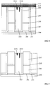
- Figures 1-5 illustrate schematic cross-section views of an NAND flash memory corresponding to certain stages of an existing fabrication method in the current technology.
- the semiconductor substrate 100 includes a core region (not labeled) and a peripheral region (not shown). For illustration purposes, only a portion of the core region is shown in Figures 1-5 , while the peripheral region is not shown.
- each gate stack structure includes a tunnel oxide layer 101, a floating gate layer 103, a dielectric layer 105, and a control gate layer 107.
- a mask layer 109 is also formed on the gate stack structures.
- a plurality of trenches 102 are formed between neighboring gate stack structures.
- a plurality of sidewalls 111 are formed on the side surfaces of the plurality of gate stack structures. The plurality of sidewalls 111 cover the bottom and the side surfaces of the plurality of trenches 102.
- a first dielectric layer 113 is formed to fill the plurality of trenches 102.
- a stop layer 115 is then formed on the surfaces of the first dielectric layer 113 and the mask layer 109. The stop layer 115 also covers the top surface of the plurality of sidewalls 111.
- a second dielectric layer (not shown) is further formed on the peripheral region (not shown) and also on the stop layer 115 of the core region.
- the second dielectric layer is intended to be formed only on the peripheral region and, thus, a subsequent process to remove the portion of the second dielectric layer formed in the core region is required.
- a planarization process is performed to remove the portion of the second dielectric layer formed on the stop layer 115.
- the planarization process is stopped when the stop layer 115 is exposed.
- the portion of the second dielectric layer formed in the core region is then removed by the planarization process.
- the remaining portion of the stop layer 115 together with the mask layer 109 (referring to Figure 2 ) and a portion of the first dielectric layer 113 are removed by an etch-back process to expose at least a portion of each gate stack structure.
- the portion of each gate stack structure exposed after the etch-back process is a portion of the control gate layer 107. That is, the top surface and a portion of the side surface of the control gate layer 107 are exposed after the etch-back process.
- a metal silicide layer 117 is formed to cover the top and the side surfaces of the exposed portion of the control gate layer 107 and also cover the first dielectric layer 113. As shown in Figure 4 , the portion of the metal silicide layer 117 covering the first dielectric layer 113 is then removed and, thus, only the portion of the metal silicide layer 117 covering the control gate layer 107 remains. The remaining portion of the metal silicide layer 117 serves as word lines 119 as shown in Figure 5 .
- voids 1131 and a variety of seams 1132 may appear in the formed first dielectric layer 113.
- the structure shown in Figure 2 is described to contain one void 1131 and one seam 1132. Any number of the voids 1131 and/or the seams 1132 can occur in the first dielectric layer.
- the void 1131 and the seam 1132 formed in the first dielectric layer 113 may be exposed at the surface of the etched first dielectric layer 113. That is, the etch-back process may be stopped at a level cutting through the void 1131 and the seam 1132.
- a first metal silicide filler 1171 may be formed in the void 1131 while a second metal silicide filler 1172 may be formed in the void 1132.
- the first metal silicide filler 1171 formed in the void 1131 and the second metal silicide filler 1172 formed in the seam 1132 may unlikely be removed.
- the first metal silicide filler 1171 and the second metal silicide filler 1172 may still remain in the first dielectric layer 113, which may lead to degraded insulating properties of the first dielectric layer 113, causing high risk of current leaking between word lines 119.
- the void 1131 and the seam 1132 may be exposed at the etched surface of the first dielectric layer 113. Further, during a subsequent cleaning process, acid treatment may enlarge the sizes of the exposed void 1131 and the exposed seam 1132. Therefore, after the deposition of the metal silicide material, more metal silicide material may be filled into the void 1131 and the seam 1132. As a result, the k value of the first dielectric layer 113 may be changed, leading to degradation of the dielectric performance.
- the amount of the first dielectric layer 113 removed by the etch-back process is relatively small, the exposed portion of the control gate layer 107 may not be sufficient, leading to insufficient amount of the metal silicide material formed on the gate electrode.
- the amount of the material of the first dielectric layer to be removed by the etch-back process may need to be strictly controlled in existing methods, thus the process window for the etch-back process may be relatively narrow.
- the stop layer 115 is often made of a nitride material.
- the nitride material usually demonstrates poor filling properties, thus during the formation of the stop layer 115, the nitride material may not be efficiently filled into the void 1131 and the seam 1132. Even in a case where a small amount of the nitride material is indeed filled into the void 1131 and the seam 1132, the electric properties of the first dielectric layer 113 may still be poor because of the huge difference between the k value of the material of the stop layer 115 and the k value of the material of the first dielectric layer 113.
- a cleaning process may be performed on the structure obtained after the etch-back process in order to ensure sufficient contact between the metal silicide layer 117 and the control gate layer 107.
- the cleaning process may enlarge the sizes of the void 1131 and the seam 1132 so that the void 1131 and the seam 1132 may more likely be filled with the metal silicide material following the process for forming the metal silicide layer 117.
- the annealing process during the formation of the metal silicide layer 117 may also make it easier for the metal silicide material to fill into the void 1131 and the seam 1132.
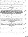
- Figure 12 shows a flowchart of an exemplary fabrication method for the NAND flash memory consistent with the disclosed embodiments.
- Figures 6-11 shows schematic views of semiconductor structures corresponding to certain stages of the exemplary fabrication method.
- FIG. 12 at the beginning of the fabrication process, a semiconductor substrate is provided (S201).
- Figure 6 shows a schematic view of the semiconductor substrate 200.
- the semiconductor substrate 200 may include a core region (not labeled) and a peripheral region (not shown). For illustration purposes, only a portion of the core region is shown in Figures 6-11 ; while the peripheral region is not shown in Figures 6-11 .
- the semiconductor substrate 200 may be a silicon substrate, a germanium substrate, or a silicon-on-insulator (SOI) substrate. In other embodiments, the semiconductor substrate 200 may also be any other appropriate substrates including III-V compound substrates such as GaAs.
- the core region may be used to form the core storage circuits of the flash memory and the peripheral region may be used to form the peripheral storage circuits of the flash memory.
- a plurality of discrete gate stack structures may be formed in the core region.
- a plurality of trenches 202 may be formed between neighboring gate stack structures.
- each gate stack structure may further include a tunnel oxide layer 201, a floating gate layer 203, a dielectric layer, and a control gate layer 207.
- the dielectric layer may be an oxide-nitride-oxide (ONO) layer 205.
- the control gate layer 207 may be made of polycrystalline silicon and may be formed by a chemical vapor deposition (CVD) method.
- the aspect ratio of the plurality of trenches 202 may be greater than 10:1.
- a first dielectric layer may be formed in each trench 202.
- the first dielectric layer may be formed by high aspect ratio process-CVD (HARP-CVD) or high density plasma-CVD (HDP-CVD).
- HTP-CVD high aspect ratio process-CVD
- HDP-CVD high density plasma-CVD
- the aspect ratio of the trenches 202 is greater than 10:1
- defects such as voids and seams may inevitably appear in the formed first dielectric layer. Such defects may further lead to various detrimental conditions for subsequent fabrication processes.
- the voids and the seams may not be essentially different, because, in general, the width of the voids may be greater than the width of the seams while the depth of the seams may be larger than the depth of the voids.
- a mask layer 209 may be formed on each control gate layer 207.
- the mask layer 209 may be made of SiN x .
- the mask layer 209 may also be a stack structure of SiO x and SiN x .
- the mask layer 209 may be formed by a CVD method. In other embodiments, the mask layer 209 may be made of any appropriate material and may be formed by any appropriate method.
- the mask layer 209 may be used to assist the formation of the plurality of gate stack structures in the core region. Specifically, a mask material layer may first be formed on both the core region and the peripheral region. Further, the mask material layer may be patterned. As shown in Figure 6 , after the patterning process, the mask layer 209 may then be formed by the remaining portion of the mask material layer in the core region. The mask layer 209 may define the plurality of gate stack structures in the core region. Moreover, a mask layer, not shown in Figure 6 , may also be formed in the peripheral region. The mask layer formed in the peripheral region may define gate stack structures in the peripheral region.
- a method forming the gate stack structures in different regions may include forming a photoresist layer on the mask material layer, patterning the photoresist layer, and then etching the mask material layer using the patterned photoresist layer as an etch mask until the control gate layer 207 in the core region is exposed. As such, the mask layer 209 may be patterned. The method further includes removing the remaining photoresist layer, and then etching the control gate layer 207, the ONO layer 205, the floating gate layer 203, and the tunnel oxide layer 201 using the mask layer 209 formed in the core region as an etch mask. After the etching process, a plurality of discrete gate stack structures may be obtained.
- each gate stack structure may include a tunnel oxide layer 201, a floating gate layer 203 formed on the tunnel oxide layer 201, an ONO layer 205 formed on the floating gate layer 203, a control gate layer 207 formed on the ONO layer 205, and a remaining mask layer 209 formed on the control gate layer 207.
- the mask layer may not be formed in the course of forming the gate stack structures. Instead, the gate stack structures may be formed by other appropriate method.
- a plurality of sidewalls 211 may be formed on the side surfaces of the plurality of gate stack structures.
- the sidewalls 211 cover the bottom surfaces and the side surfaces of the plurality of trenches 202 formed between neighboring gate stack structures.
- the plurality of sidewalls 211 may also cover the side surfaces of the mask layer 209.
- a first dielectric layer may be formed in each trench (S202).
- Figure 7 shows a schematic cross-section view of the corresponding semiconductor structure.
- a first dielectric layer 213 may be formed to fill the plurality of trenches 202.
- the first dielectric layer 213 may be made of SiO x .
- the first dielectric layer 213 may be formed by HARP-CVD or HDP-CVD.
- compressive stress may exist in dielectric layer formed by HDP-CVD while tensile stress may exist in dielectric layer formed by HARP-CVD.
- the subsequently-formed first dielectric layer may contain a number of defects, such as voids, seams, etc., because the aspect ratio of the trenches 202 is greater than 10:1.
- the structure shown in Figure 7 is described to contain one void 2131 and one seam 2132.
- the number of the voids 2131 and/or the number of the seams 2132 in the first dielectric layer 213 may be more than one.
- a flowable dielectric layer may be formed on the first dielectric layer and the mask layer, and then a solidification process may be performed on the flowable dielectric layer to form a solid dielectric layer (S203).
- Figure 8 shows a schematic cross-section view of the corresponding semiconductor structure.
- a flowable dielectric layer may be formed on the surfaces of the first dielectric layer 213 and the mask layer 209.
- the flowable dielectric layer may also cover the top surfaces of the sidewalls 211.
- a solidification treatment process may be performed on the flowable dielectric layer to convert the flowable dielectric layer into a solid dielectric layer 215. That is, the solid dielectric layer 215 is formed from the flowable dielectric layer through the solidification treatment process.
- the solid dielectric layer 215 may be situated on the surfaces of the first dielectric layer 213 and the mask layer 209 as well as the top surfaces of the sidewalls 211.
- the flowable dielectric layer may fill into the void 2131 and the seam 2132.
- the flowable dielectric layer filled into the void 2131 may form a solid dielectric filler 2151 and the flowable dielectric layer filled into the seam 2132 may form a solid dielectric filler 2152.
- Each of the solid dielectric filler 2151 and the solid dielectric filler 2152 may be a portion of the solid dielectric layer 215.
- the solid dielectric layer may be formed on the first dielectric layer and the top surfaces of the plurality of gate stack structures.
- the flowable dielectric layer may be a flowable polymer.
- the solid dielectric layer 215 may be made of SiO x .
- the flowable polymer and SiO x may be formed by a fluid CVD method.
- the fluid CVD method may include a deposition process and a conversion process following the deposition process. Specifically, during the deposition process, a silica (SiO x ) precursor may be used to form flowable polymer through free radical polymerization, while during the conversion process, ozone steam may be used to convert the flowable polymer into SiO x through oxidation.
- the silica precursor may be used to react with ammonia plasma to form a flowable polymer and thus fill the void 2131 and the seam 2132.
- the thickness of the flowable polymer may be defined by the corresponding process time.
- the flowable polymer may be oxidized when the temperature of the ozone steam is controlled in a range of 100 °C to 200 °C. At a temperature between 100 °C and 200 °C, oxidation of the flowable polymer by ozone steam may be uniform and stable. Therefore, after performing the solidification treatment process, the flowable polymer may form solid SiO 2 , i.e. the solid dielectric layer 215.
- the thickness of the solid dielectric layer 215 may be controlled to be above 200 ⁇ so that the solid dielectric filler 2151 and the solid dielectric filler 2152 may completely fill the void 2131 and the seam 2132.
- the dielectric layer 215 may also meet the requirements of subsequent fabrication processes. In particular, the dielectric layer 215 may meet the requirement for subsequently performing an etch-back process.
- the flowable dielectric layer may be made of graphene oxide or graphite oxide. That is, graphene oxide or graphite oxide may be used for forming the flowable dielectric layer and fill the void 2131 and the seam 2132.
- the solid dielectric layer 215 may be made of solidified graphene oxide or solidified graphite oxide obtained after performing the solidification treatment process.
- a specific method to form the flowable dielectric layer using graphene oxide and to fill the void 2131 and the seam 2132 may include performing a plasma treatment process on the surface of the structure shown in Figure 7 .
- the plasma treatment process may use nitrogen as a reaction gas source to generate plasma.
- the method may further include forming a copper layer on the surface of the structure after performing the plasma treatment process.
- the copper layer may be formed by sputtering. Further, the copper layer may fill the void 2131 and the seam 2132.
- the method may then include forming a graphene oxide layer on the copper layer through a CVD process and then forming a polymethyl methacrylate (PMMA) layer on the graphene oxide layer.
- PMMA polymethyl methacrylate
- the method may further include performing a wet etching process to remove the copper layer.
- the portion of the copper layer filled in the void 2131 and the seam 2132 may be removed by the wet etching process so that the void 2131 and the seam 2132 may be exposed again.
- the graphene oxide layer may replace the original copper layer and thus may be settled down on the surface of the structure shown in Figure 7 .
- the graphene oxide layer may also fill the re-exposed void 2131 and the seam 2132.
- the method may include removing the PMMA layer and performing a solidification treatment process such as a baking process to solidify the graphene oxide layer.
- a method to form graphene oxide from natural graphite may include the following steps. First, at a temperature of 80 °C, a certain amount of natural graphite, concentrated sulfuric acid, K 2 S 2 O 8 , and P 2 O 5 may be mixed together. A mixing time of 4 hours may be used for the mixing process. The obtained mixture may then be cooled down to room temperature. Further, the mixture may be diluted with deionized water. After 12 hours of settling, the mixture may be separated by centrifuge technology and then may be rinsed by deionized water again to obtain pre-oxidized graphite.
- Concentrated sulfuric acid and KMnO 4 may then be used to further oxidize the pre-oxidized graphite for 2 hours with the reaction mixture sitting in an ice-water bath. Further, the reoxidized mixture may be diluted with deionized water and may be kept in an ice-water bath for 2 more hours. The mixture may be diluted with deionized water again and then may be mixed with H 2 O 2 to allow further oxidization. After oxidization using H 2 O 2 , the mixture may be separated by centrifuge technology and then may be rinsed by HCl acid and deionized water to finally obtain graphene oxide with desired water-solubility and flowability. Therefore, the graphene oxide formed following the above fabrication procedure may be used as the flowable dielectric layer.
- a stop layer may be formed on the solid dielectric layer (S204).
- Figure 8 shows a schematic cross-section view of the corresponding semiconductor structure with a stop layer 217 formed on the solid dielectric layer 215.
- a second dielectric layer may be formed to cover the peripheral region (S205). Specifically, after forming the stop layer 217, a second dielectric layer (not shown) may be further formed on the peripheral region (not shown) and also on the stop layer 217 in the core region. The second dielectric layer may be intended to be formed only on the peripheral region. Therefore, the portion of the second dielectric layer formed in the core region may need to be removed by a subsequent process.
- a planarization process may be performed to remove the portion of the second dielectric layer formed on the stop layer 217.
- the planarization process may be stopped as the stop layer 217 is reached.
- the portion of the second dielectric layer formed in the core region may be removed by the planarization process.
- CMP chemical mechanical polishing
- FIG. 9 shows a schematic cross-section view of the corresponding semiconductor structure.
- the remaining portion of the stop layer 217 together with the mask layer 209 (referring to Figure 8 ), the solid dielectric layer 215, and a portion of the first dielectric layer 213 may be removed by an etch-back process to expose at least a portion of the gate stack structures.
- the portion of each gate stack structure exposed after the etch-back process is the control gate layer 207.
- the top surface and a portion of the side surface of the control gate layer 207 may be exposed after the etch-back process.
- a dry etching method may be used in the etch-back process. Further, the etch-back process may expose the side surfaces of at least a top portion of the control gate layer 207.
- the reaction gas used in the etch-back process may include CF.
- a portion of the solid dielectric layer 215 may remain on the first dielectric layer 213 after the etch-back process. In certain other circumstances, the remaining solid dielectric layer 215 may only fill the void 2131 and the seam 2132 situated in the top portion of the first dielectric layer 213. That is, the solid dielectric filler 2151 and the solid dielectric filler 2152 shown in Figure 9 may be the only remaining portion of the solid dielectric layer 215 after the etch-back process.
- the etch-back process may completely remove the portion of the solid dielectric layer 215 formed on the first dielectric layer 213 and only retain the solid dielectric filler 2151 and the solid dielectric filler 2152, i.e. the portion of the solid dielectric layer 215 filled into the void 2131 and the seam 2132, respectively.
- a solid dielectric layer 215 with a thickness in the range discussed above may ensure the successful performance of the etch-back process and the realization of the desired structure following the etch-back process.
- the etch-back process may not only etch the remaining portion of the stop layer 217 and the first dielectric layer 213, but also simultaneously etch the mask layer 209. In other embodiments, when the mask layer 209 is not formed, the etch-back process may not include etching the mask layer 209.
- a metal silicide layer may be formed on the exposed portion of the gate stack structures, the first dielectric layer, and the solid dielectric layer (S207).
- Figure 10 shows a schematic cross-section view of the corresponding semiconductor structure.
- a metal silicide layer 219 may be formed to cover the exposed portion of the gate stack structures, the first dielectric layer 213, and the remaining portion of the solid dielectric layer 215. Prior to the formation of the metal silicide layer 219, a cleaning process may often be performed on the semiconductor substrate obtained through the fabrication process described above.
- the metal silicide layer 219 may be formed to cover the surface of the exposed portion of the gate stack structures after the etch-back process. That is, the metal silicide layer 219 may cover the top surface and a portion of the side surface of each control gate layer 207, the first dielectric layer 213, and the remaining portion of the solid dielectric layer 215.
- the metal silicide layer 219 may be made of NiSi, WSi, MoSi, TiSi, CoSi, or TISi.
- the metal silicide layer 219 may be formed by a process including steps such as rapid thermal annealing, etc.
- Figure 11 shows a schematic cross-section view of the corresponding semiconductor structure.
- the portion of the metal silicide layer 219 formed on the solid dielectric layer 215 and the first dielectric layer 213 may be removed. After the removal of the portion of the metal silicide layer 219, only the portion of the metal silicide layer 219 formed on the plurality of control gate layers 207 may be retained. The remaining portion of the metal silicide layer 219 may be used as word lines 221.
- the portion of the metal silicide layer 219 formed on the solid dielectric layer 215 and the first dielectric layer 213 may be removed by a wet etching process. Further, during the formation of the solid dielectric layer 215, the solid dielectric filler 2151 and the solid dielectric filler 2152 may also be formed in the corresponding void 2131 and the seam 2132, respectively. That is, the void 2131 and the seam 2132 maybe filled with a solid dielectric material prior to forming the metal silicide layer 219 so that the metal silicide layer 219 may not enter the void 2131 and the seam 2132. Therefore, the entire portion of metal silicide layer 219 formed on the solid dielectric layer 215 and the first dielectric layer 213 may be completely removed without leaving any residue in the solid dielectric layer 215 or in the first dielectric layer 213.
- a flowable dielectric layer may be formed on the surface of the plurality of gate dielectric structures and the surface of the first dielectric layer 213 after performing an etch-back process.
- the flowable dielectric layer may then be solidified to form a solid dielectric layer 215.
- a metal silicide layer 219 may be formed on the solid dielectric layer 215, the first dielectric layer 213, and the gate stack structures during a subsequent process.
- the portion of the metal silicide layer 219 formed on the solid dielectric layer 215 and the first dielectric layer 213 may be removed, and thus only the top surfaces of the gate stack structures may be covered by the metal silicide layer 219 in the finished structure of the NAND flash memory.
- the flowable dielectric layer may fill corresponding voids 2131 and seams 2132 situated in the top portion of the first dielectric layer 213. Subsequently, after performing a solidification treatment process, the flowable dielectric layer may be converted into a solid dielectric layer 215. In the meantime, the portion of flowable dielectric layer filled in the voids 2131 may become solid dielectric filler 2151 while the portion of flowable dielectric layer filled in the seams 2132 may become solid dielectric filler 2152.
- the metal silicide layer 219 when the metal silicide layer 219 is further formed on the solid dielectric layer 215 and the first dielectric layer 213, the voids 2131 and the seams 2132 may still be filled by solid dielectric filler 2151 and solid dielectric filler 2152, respectively. Therefore, the metal silicide layer 219 may not be able to enter the voids 2131 or the seams 2132. Thus, after removing the portion of the metal silicide layer 219 formed on the solid dielectric layer 215 and the first dielectric layer 213, no residue of the metal silicide layer 219 may be left in the first dielectric layer 213.
- the solid dielectric layer 215 may be formed from the flowable dielectric layer by performing a solidification treatment process. Because of the specific formation method of the solid dielectric layer 215, voids and seams may not likely appear in the formed solid dielectric layer 215. Therefore, residue of the metal silicide layer 219 may not be expected to appear in the solid dielectric layer 215.
- the disclosed method may improve the dielectric performance of the dielectric layer (including both the first dielectric layer 213 and the solid dielectric layer 215) between word lines 221 and, thus, the risk of current leaking between word lines 221 may be reduced.
- the disclosed method may prevent leaving metal silicide residue in the dielectric layer between neighboring word lines 221, the amount of material removed by the etch-back process may not need to be strictly controlled. Therefore, the disclosed method may improve the process window for the etch-back process, and thus improve the process window for the entire fabrication process for the NAND flash memory.
Landscapes
- Engineering & Computer Science (AREA)
- Manufacturing & Machinery (AREA)
- Semiconductor Memories (AREA)
- Non-Volatile Memory (AREA)
- Chemical & Material Sciences (AREA)
- Crystallography & Structural Chemistry (AREA)
- Physics & Mathematics (AREA)
- Plasma & Fusion (AREA)
Abstract
Description
- This application claims the priority of Chinese Patent Application No.
CN201510919128.2, filed on December 10,2015 - The present invention generally relates to the field of semiconductor fabrication technology and, more particularly, relates to an NAND flash memory and fabrication methods thereof.
- As compared to hard disk drives, Not AND (NAND) flash memory provides a more advanced data-storage method. Specifically, by using page as unit for data reading and data writing, NAND flash memory is a desired solution for storing continuous data, such as images, audio, and other types of data files. In the meantime, because of the advantages that NAND flash memory demonstrates, e.g. low product cost, large storage capacity, and fast writing and fast erasing, NAND flash memory has been widely used in the field of mobile communication devices and portable multimedia devices.
- However, for NAND flash memory fabricated by existing methods, the risk of current leaking between word lines may be high. The disclosed fabrication method and NAND flash memory are directed to solve one or more problems set forth above and other problems in the art.
- A first aspect of the present invention includes a method for fabricating an NAND flash memory. The method includes providing a semiconductor substrate with a core region and a peripheral region, forming a plurality of discrete gate stack structures in the core region with neighboring gate stack structures separated by a trench, and forming a first dielectric layer to fill each trench. The method further includes forming a flowable dielectric layer on the first dielectric layer and the gate stack structures, and then performing a solidification treatment process on the flowable dielectric layer to form a solid dielectric layer. Voids and seams formed in the top portion of the first dielectric layer are filled by the solid dielectric layer. The method also includes removing the solid dielectric layer and a portion of the first dielectric layer to expose at least a top portion of the gate stack structures, forming a metal silicide layer on an exposed portion of the gate stack structures and the first dielectric layer, and then removing a portion of the metal silicide layer formed on the first dielectric layer.
- After performing the solidification treatment process, the method may further include: forming a stop layer on the solid dielectric layer; forming a second dielectric layer on the stop layer and on the peripheral region; performing a planarization process until reaching the stop layer to remove a portion of the second dielectric layer formed on the stop layer; and removing a remaining portion of the stop layer.
- Preferably, each gate stack structure further includes a tunnel oxide layer, a floating gate layer, a dielectric layer, and a control gate layer formed sequentially on the semiconductor substrate.
- Preferably, the dielectric layer formed in each gate stack structure is an oxide-nitride-oxide layer.
- Preferably, the flowable dielectric layer is made of a flowable polymer. The flowable polymer may be oxidized in an ozone steam at a temperature in a range of 100 °C to 200 °C.
- Preferably, the solid dielectric layer is made of SiOx.
- Preferably, the flowable polymer and SiOx are deposited by fluid chemical vapor deposition. The fluid chemical vapor deposition may include: a deposition process using SiOx precursor to form flowable polymer through free radical polymerization; and a conversion process to form SiOx by using ozone steam to oxidize the flowable polymer.
- Preferably, a thickness of the solid dielectric layer is greater than 200 Å.
- Preferably, a dry etching method is used during the etch-back process.
- Preferably, a reaction gas used in the etch-back process includes CF.
- Preferably, the etch-back process exposes at least a portion of the side surface of the control gate layer.
- Preferably, the metal silicide layer is made of one of NiSi, WSi, MoSi, TiSi, CoSi, and TISi.
- Preferably, the first dielectric layer is formed by a high aspect ratio process-chemical vapor deposition (HARP-CVD) method or a high density plasma-chemical vapor deposition (HDP-CVD) method.
- Preferably, the aspect ratio of the trench is greater than 10:1.
- Prior to the formation of the stop layer, a mask layer may be formed on the gate stack structures, and the etch-back process performed to etch the remaining portion of the stop layer and the first dielectric layer may also etch the mask layer. Preferably, the mask layer is a SiN layer or a stack structure of SiOx and SiN.
- Preferably, the flowable dielectric layer is graphene oxide or graphite oxide.
- Preferably, the planarization process performed on the second dielectric layer is a chemical mechanical polishing process.
- Prior to forming the metal silicide layer, a cleaning process may be performed on a semiconductor structure obtained after the etch-back process.
- Preferably, a remaining portion of the metal silicide layer on each gate stack structure is used as a word line.
- A second aspect of the present invention provides an NAND flash memory. The NAND flash memory includes a semiconductor substrate including a core region and a peripheral region, a plurality of discrete gate stack structures formed in the core region with neighboring gate stack structures separated by a trench, and a first dielectric layer filling up each trench. Voids and seams formed in the top portion of the first dielectric layer are filled by a solid dielectric layer. The solid dielectric layer is formed through a solidification treatment process performed on a flowable dielectric layer formed on the first dielectric layer. The solid dielectric layer formed above the top surface of the first dielectric layer is then removed. The NAND flash memory further includes a second dielectric layer formed on the peripheral region, and a metal silicide layer formed on a top surface of each gate stack structure. The metal silicide layer formed on each gate stack structure serves as a word line.
- Preferably, each gate stack structure further includes a tunnel oxide layer, a floating gate layer, a dielectric layer, and a control gate layer formed sequentially on the semiconductor substrate.
- Preferably, the flowable dielectric layer is made of a flowable polymer.
- Preferably, the solid dielectric layer is made of SiOx.
- Preferably, the flowable polymer and SiOx are deposited by fluid chemical vapor deposition.
- Other aspects of the present invention can be understood by those skilled in the art in light of the description, the claims, and the drawings of the present invention.
- The following drawings are merely examples for illustrative purposes according to various disclosed embodiments and are not intended to limit the scope of the present invention.
-
Figures 1-5 illustrate schematic views of semiconductor structures corresponding to certain stages of an existing fabrication method for an NAND flash memory; -
Figures 6-11 illustrate schematic views of semiconductor structures corresponding to certain stages of an exemplary fabrication method consistent with various disclosed embodiments; -
Figure 12 illustrates a flowchart of the exemplary fabrication process for an NAND flash memory consistent with disclosed embodiments. - Reference will now be made in detail to exemplary embodiments of the invention, which are illustrated in the accompanying drawings. Wherever possible, the same reference numbers will be used throughout the drawings to refer to the same or like parts.
-
Figures 1-5 illustrate schematic cross-section views of an NAND flash memory corresponding to certain stages of an existing fabrication method in the current technology. - Referring to
Figure 1 , asemiconductor substrate 100 is provided. Thesemiconductor substrate 100 includes a core region (not labeled) and a peripheral region (not shown). For illustration purposes, only a portion of the core region is shown inFigures 1-5 , while the peripheral region is not shown. - Referring to
Figure 1 , a plurality of discrete gate stack structures (not labeled) are formed on the core region. From the bottom to the top, each gate stack structure includes atunnel oxide layer 101, afloating gate layer 103, adielectric layer 105, and acontrol gate layer 107. In addition, amask layer 109 is also formed on the gate stack structures. Further, a plurality oftrenches 102 are formed between neighboring gate stack structures. A plurality ofsidewalls 111 are formed on the side surfaces of the plurality of gate stack structures. The plurality ofsidewalls 111 cover the bottom and the side surfaces of the plurality oftrenches 102. - Further, referring to
Figure 2 , a firstdielectric layer 113 is formed to fill the plurality oftrenches 102. Astop layer 115 is then formed on the surfaces of thefirst dielectric layer 113 and themask layer 109. Thestop layer 115 also covers the top surface of the plurality ofsidewalls 111. - After forming the
stop layer 115, a second dielectric layer (not shown) is further formed on the peripheral region (not shown) and also on thestop layer 115 of the core region. The second dielectric layer is intended to be formed only on the peripheral region and, thus, a subsequent process to remove the portion of the second dielectric layer formed in the core region is required. - For example, a planarization process is performed to remove the portion of the second dielectric layer formed on the
stop layer 115. The planarization process is stopped when thestop layer 115 is exposed. Thus, the portion of the second dielectric layer formed in the core region is then removed by the planarization process. - Referring to
Figure 3 , the remaining portion of thestop layer 115 together with the mask layer 109 (referring toFigure 2 ) and a portion of thefirst dielectric layer 113 are removed by an etch-back process to expose at least a portion of each gate stack structure. As shown inFigure 3 , the portion of each gate stack structure exposed after the etch-back process is a portion of thecontrol gate layer 107. That is, the top surface and a portion of the side surface of thecontrol gate layer 107 are exposed after the etch-back process. - Referring to
Figure 4 andFigure 5 , ametal silicide layer 117 is formed to cover the top and the side surfaces of the exposed portion of thecontrol gate layer 107 and also cover thefirst dielectric layer 113. As shown inFigure 4 , the portion of themetal silicide layer 117 covering thefirst dielectric layer 113 is then removed and, thus, only the portion of themetal silicide layer 117 covering thecontrol gate layer 107 remains. The remaining portion of themetal silicide layer 117 serves asword lines 119 as shown inFigure 5 . - However, referring to
Figure 2 , during the formation of thefirst dielectric layer 113, a variety ofvoids 1131 and a variety ofseams 1132 may appear in the formed firstdielectric layer 113. For illustration purposes, the structure shown inFigure 2 is described to contain onevoid 1131 and oneseam 1132. Any number of thevoids 1131 and/or theseams 1132 can occur in the first dielectric layer. - As shown in
Figure 3 , after performing the etch-back process, thevoid 1131 and theseam 1132 formed in thefirst dielectric layer 113 may be exposed at the surface of the etched firstdielectric layer 113. That is, the etch-back process may be stopped at a level cutting through thevoid 1131 and theseam 1132. - Further, during the formation of the
metal silicide layer 117, when the metal silicide material is formed to cover thefirst dielectric layer 113, thevoid 1131 and theseam 1132 may also be filled. Specifically, referring toFigure 4 , a firstmetal silicide filler 1171 may be formed in thevoid 1131 while a secondmetal silicide filler 1172 may be formed in thevoid 1132. - Further, referring to
Figure 5 , when the portion of themetal silicide layer 117 formed on thefirst dielectric layer 113 is removed, the firstmetal silicide filler 1171 formed in thevoid 1131 and the secondmetal silicide filler 1172 formed in theseam 1132 may unlikely be removed. As a result, the firstmetal silicide filler 1171 and the secondmetal silicide filler 1172 may still remain in thefirst dielectric layer 113, which may lead to degraded insulating properties of thefirst dielectric layer 113, causing high risk of current leaking between word lines 119. - Moreover, because of the presence of the
void 1131 and theseam 1132, when the amount of thefirst dielectric layer 113 removed by the etch-back process is relatively large, thevoid 1131 and theseam 1132 may be exposed at the etched surface of thefirst dielectric layer 113. Further, during a subsequent cleaning process, acid treatment may enlarge the sizes of the exposedvoid 1131 and the exposedseam 1132. Therefore, after the deposition of the metal silicide material, more metal silicide material may be filled into thevoid 1131 and theseam 1132. As a result, the k value of thefirst dielectric layer 113 may be changed, leading to degradation of the dielectric performance. On the other hand, when the amount of thefirst dielectric layer 113 removed by the etch-back process is relatively small, the exposed portion of thecontrol gate layer 107 may not be sufficient, leading to insufficient amount of the metal silicide material formed on the gate electrode. As electrical signals in NAND flash memory is conducted through themetal silicide layer 117, insufficient amount of the metal silicide material may further cause degradation of the performance of the NAND flash memory. Therefore, the amount of the material of the first dielectric layer to be removed by the etch-back process may need to be strictly controlled in existing methods, thus the process window for the etch-back process may be relatively narrow. - Specifically, the
stop layer 115 is often made of a nitride material. The nitride material usually demonstrates poor filling properties, thus during the formation of thestop layer 115, the nitride material may not be efficiently filled into thevoid 1131 and theseam 1132. Even in a case where a small amount of the nitride material is indeed filled into thevoid 1131 and theseam 1132, the electric properties of thefirst dielectric layer 113 may still be poor because of the huge difference between the k value of the material of thestop layer 115 and the k value of the material of thefirst dielectric layer 113. - Moreover, prior to forming the
metal silicide layer 117, a cleaning process may be performed on the structure obtained after the etch-back process in order to ensure sufficient contact between themetal silicide layer 117 and thecontrol gate layer 107. However, the cleaning process may enlarge the sizes of thevoid 1131 and theseam 1132 so that thevoid 1131 and theseam 1132 may more likely be filled with the metal silicide material following the process for forming themetal silicide layer 117. In addition, the annealing process during the formation of themetal silicide layer 117 may also make it easier for the metal silicide material to fill into thevoid 1131 and theseam 1132. - In view of the above problems in existing methods, the present invention provides an improved method for forming an NAND flash memory.
Figure 12 shows a flowchart of an exemplary fabrication method for the NAND flash memory consistent with the disclosed embodiments.Figures 6-11 shows schematic views of semiconductor structures corresponding to certain stages of the exemplary fabrication method. - Referring to
Figure 12 , at the beginning of the fabrication process, a semiconductor substrate is provided (S201).Figure 6 shows a schematic view of thesemiconductor substrate 200. - Referring to
Figure 6 , thesemiconductor substrate 200 may include a core region (not labeled) and a peripheral region (not shown). For illustration purposes, only a portion of the core region is shown inFigures 6-11 ; while the peripheral region is not shown inFigures 6-11 . - In one embodiment, the
semiconductor substrate 200 may be a silicon substrate, a germanium substrate, or a silicon-on-insulator (SOI) substrate. In other embodiments, thesemiconductor substrate 200 may also be any other appropriate substrates including III-V compound substrates such as GaAs. - In one embodiment, the core region may be used to form the core storage circuits of the flash memory and the peripheral region may be used to form the peripheral storage circuits of the flash memory.
- Further, a plurality of discrete gate stack structures (not labeled) may be formed in the core region. In addition, a plurality of
trenches 202 may be formed between neighboring gate stack structures. - In one embodiment, from the bottom to the top, each gate stack structure may further include a
tunnel oxide layer 201, a floatinggate layer 203, a dielectric layer, and acontrol gate layer 207. The dielectric layer may be an oxide-nitride-oxide (ONO)layer 205. Thecontrol gate layer 207 may be made of polycrystalline silicon and may be formed by a chemical vapor deposition (CVD) method. - In one embodiment, the aspect ratio of the plurality of
trenches 202 may be greater than 10:1. In a subsequent process, a first dielectric layer may be formed in eachtrench 202. Specifically, the first dielectric layer may be formed by high aspect ratio process-CVD (HARP-CVD) or high density plasma-CVD (HDP-CVD). When the aspect ratio of thetrenches 202 is greater than 10:1, no matter which existing deposition method is adopted to form the first dielectric layer, defects such as voids and seams may inevitably appear in the formed first dielectric layer. Such defects may further lead to various detrimental conditions for subsequent fabrication processes. To certain extent, the voids and the seams may not be essentially different, because, in general, the width of the voids may be greater than the width of the seams while the depth of the seams may be larger than the depth of the voids. - Referring to
Figure 6 , amask layer 209 may be formed on eachcontrol gate layer 207. Themask layer 209 may be made of SiNx. Themask layer 209 may also be a stack structure of SiOx and SiNx. Themask layer 209 may be formed by a CVD method. In other embodiments, themask layer 209 may be made of any appropriate material and may be formed by any appropriate method. - In one embodiment, the
mask layer 209 may be used to assist the formation of the plurality of gate stack structures in the core region. Specifically, a mask material layer may first be formed on both the core region and the peripheral region. Further, the mask material layer may be patterned. As shown inFigure 6 , after the patterning process, themask layer 209 may then be formed by the remaining portion of the mask material layer in the core region. Themask layer 209 may define the plurality of gate stack structures in the core region. Moreover, a mask layer, not shown inFigure 6 , may also be formed in the peripheral region. The mask layer formed in the peripheral region may define gate stack structures in the peripheral region. - Specifically, a method forming the gate stack structures in different regions may include forming a photoresist layer on the mask material layer, patterning the photoresist layer, and then etching the mask material layer using the patterned photoresist layer as an etch mask until the
control gate layer 207 in the core region is exposed. As such, themask layer 209 may be patterned. The method further includes removing the remaining photoresist layer, and then etching thecontrol gate layer 207, theONO layer 205, the floatinggate layer 203, and thetunnel oxide layer 201 using themask layer 209 formed in the core region as an etch mask. After the etching process, a plurality of discrete gate stack structures may be obtained. Moreover, each gate stack structure may include atunnel oxide layer 201, a floatinggate layer 203 formed on thetunnel oxide layer 201, anONO layer 205 formed on the floatinggate layer 203, acontrol gate layer 207 formed on theONO layer 205, and a remainingmask layer 209 formed on thecontrol gate layer 207. - In other embodiments, the mask layer may not be formed in the course of forming the gate stack structures. Instead, the gate stack structures may be formed by other appropriate method.
- In one embodiment, a plurality of
sidewalls 211 may be formed on the side surfaces of the plurality of gate stack structures. Thesidewalls 211 cover the bottom surfaces and the side surfaces of the plurality oftrenches 202 formed between neighboring gate stack structures. In addition, the plurality ofsidewalls 211 may also cover the side surfaces of themask layer 209. - Further, returning to
Figure 12 , a first dielectric layer may be formed in each trench (S202).Figure 7 shows a schematic cross-section view of the corresponding semiconductor structure. - Referring to
Figure 7 , a firstdielectric layer 213 may be formed to fill the plurality oftrenches 202. In one embodiment, thefirst dielectric layer 213 may be made of SiOx. Thefirst dielectric layer 213 may be formed by HARP-CVD or HDP-CVD. Generally, compressive stress may exist in dielectric layer formed by HDP-CVD while tensile stress may exist in dielectric layer formed by HARP-CVD. However, regardless of which one of the two methods being used, the subsequently-formed first dielectric layer may contain a number of defects, such as voids, seams, etc., because the aspect ratio of thetrenches 202 is greater than 10:1. For illustration purposes, the structure shown inFigure 7 is described to contain onevoid 2131 and oneseam 2132. One may note that in practice, the number of thevoids 2131 and/or the number of theseams 2132 in thefirst dielectric layer 213 may be more than one. - Further, returning to
Figure 12 , a flowable dielectric layer may be formed on the first dielectric layer and the mask layer, and then a solidification process may be performed on the flowable dielectric layer to form a solid dielectric layer (S203).Figure 8 shows a schematic cross-section view of the corresponding semiconductor structure. - Referring to
Figure 8 , a flowable dielectric layer may be formed on the surfaces of thefirst dielectric layer 213 and themask layer 209. The flowable dielectric layer may also cover the top surfaces of thesidewalls 211. Then, a solidification treatment process may be performed on the flowable dielectric layer to convert the flowable dielectric layer into asolid dielectric layer 215. That is, thesolid dielectric layer 215 is formed from the flowable dielectric layer through the solidification treatment process. Thesolid dielectric layer 215 may be situated on the surfaces of thefirst dielectric layer 213 and themask layer 209 as well as the top surfaces of thesidewalls 211. - In one embodiment, because the flowable dielectric layer is formed on the
first dielectric layer 213 containing a void 2131 and aseam 2132, the flowable dielectric layer may fill into thevoid 2131 and theseam 2132. After performing the solidification treatment process, the flowable dielectric layer filled into thevoid 2131 may form asolid dielectric filler 2151 and the flowable dielectric layer filled into theseam 2132 may form asolid dielectric filler 2152. Each of thesolid dielectric filler 2151 and thesolid dielectric filler 2152 may be a portion of thesolid dielectric layer 215. - In other embodiments, when no mask layer is formed on the gate stack structures, the solid dielectric layer may be formed on the first dielectric layer and the top surfaces of the plurality of gate stack structures.
- In one embodiment, the flowable dielectric layer may be a flowable polymer. The
solid dielectric layer 215 may be made of SiOx. The flowable polymer and SiOx may be formed by a fluid CVD method. The fluid CVD method may include a deposition process and a conversion process following the deposition process. Specifically, during the deposition process, a silica (SiOx) precursor may be used to form flowable polymer through free radical polymerization, while during the conversion process, ozone steam may be used to convert the flowable polymer into SiOx through oxidation. - Moreover, during the deposition process, the silica precursor may be used to react with ammonia plasma to form a flowable polymer and thus fill the
void 2131 and theseam 2132. The thickness of the flowable polymer may be defined by the corresponding process time. - During the solidification treatment process, the flowable polymer may be oxidized when the temperature of the ozone steam is controlled in a range of 100 °C to 200 °C. At a temperature between 100 °C and 200 °C, oxidation of the flowable polymer by ozone steam may be uniform and stable. Therefore, after performing the solidification treatment process, the flowable polymer may form solid SiO2, i.e. the
solid dielectric layer 215. - In one embodiment, the thickness of the
solid dielectric layer 215 may be controlled to be above 200 Å so that thesolid dielectric filler 2151 and thesolid dielectric filler 2152 may completely fill thevoid 2131 and theseam 2132. In addition, with a thickness above 200 Å, thedielectric layer 215 may also meet the requirements of subsequent fabrication processes. In particular, thedielectric layer 215 may meet the requirement for subsequently performing an etch-back process. - In certain other embodiments, the flowable dielectric layer may be made of graphene oxide or graphite oxide. That is, graphene oxide or graphite oxide may be used for forming the flowable dielectric layer and fill the
void 2131 and theseam 2132. Correspondingly, thesolid dielectric layer 215 may be made of solidified graphene oxide or solidified graphite oxide obtained after performing the solidification treatment process. - A specific method to form the flowable dielectric layer using graphene oxide and to fill the
void 2131 and theseam 2132 may include performing a plasma treatment process on the surface of the structure shown inFigure 7 . The plasma treatment process may use nitrogen as a reaction gas source to generate plasma. The method may further include forming a copper layer on the surface of the structure after performing the plasma treatment process. The copper layer may be formed by sputtering. Further, the copper layer may fill thevoid 2131 and theseam 2132. The method may then include forming a graphene oxide layer on the copper layer through a CVD process and then forming a polymethyl methacrylate (PMMA) layer on the graphene oxide layer. The PMMA layer may be used to protect the graphene oxide layer. The method may further include performing a wet etching process to remove the copper layer. The portion of the copper layer filled in thevoid 2131 and theseam 2132 may be removed by the wet etching process so that thevoid 2131 and theseam 2132 may be exposed again. After the removal of the copper layer, the graphene oxide layer may replace the original copper layer and thus may be settled down on the surface of the structure shown inFigure 7 . In addition, the graphene oxide layer may also fill there-exposed void 2131 and theseam 2132. Finally, the method may include removing the PMMA layer and performing a solidification treatment process such as a baking process to solidify the graphene oxide layer. - In the fabrication process described above, a method to form graphene oxide from natural graphite may include the following steps. First, at a temperature of 80 °C, a certain amount of natural graphite, concentrated sulfuric acid, K2S2O8, and P2O5 may be mixed together. A mixing time of 4 hours may be used for the mixing process. The obtained mixture may then be cooled down to room temperature. Further, the mixture may be diluted with deionized water. After 12 hours of settling, the mixture may be separated by centrifuge technology and then may be rinsed by deionized water again to obtain pre-oxidized graphite. Concentrated sulfuric acid and KMnO4 may then be used to further oxidize the pre-oxidized graphite for 2 hours with the reaction mixture sitting in an ice-water bath. Further, the reoxidized mixture may be diluted with deionized water and may be kept in an ice-water bath for 2 more hours. The mixture may be diluted with deionized water again and then may be mixed with H2O2 to allow further oxidization. After oxidization using H2O2, the mixture may be separated by centrifuge technology and then may be rinsed by HCl acid and deionized water to finally obtain graphene oxide with desired water-solubility and flowability. Therefore, the graphene oxide formed following the above fabrication procedure may be used as the flowable dielectric layer.
- Returning to
Figure 12 , further, a stop layer may be formed on the solid dielectric layer (S204).Figure 8 shows a schematic cross-section view of the corresponding semiconductor structure with astop layer 217 formed on thesolid dielectric layer 215. - Further, returning to
Figure 12 , a second dielectric layer may be formed to cover the peripheral region (S205). Specifically, after forming thestop layer 217, a second dielectric layer (not shown) may be further formed on the peripheral region (not shown) and also on thestop layer 217 in the core region. The second dielectric layer may be intended to be formed only on the peripheral region. Therefore, the portion of the second dielectric layer formed in the core region may need to be removed by a subsequent process. - Specifically, a planarization process may be performed to remove the portion of the second dielectric layer formed on the
stop layer 217. The planarization process may be stopped as thestop layer 217 is reached. Thus, the portion of the second dielectric layer formed in the core region may be removed by the planarization process. In one embodiment, a chemical mechanical polishing (CMP) method may be used in the planarization process. - Further, returning to
Figure 12 , at least a top portion of the gate stack structures may be exposed by performing an etch-back process (S206).Figure 9 shows a schematic cross-section view of the corresponding semiconductor structure. - Referring to
Figure 9 , the remaining portion of thestop layer 217 together with the mask layer 209 (referring toFigure 8 ), thesolid dielectric layer 215, and a portion of thefirst dielectric layer 213 may be removed by an etch-back process to expose at least a portion of the gate stack structures. The portion of each gate stack structure exposed after the etch-back process is thecontrol gate layer 207. Specifically, the top surface and a portion of the side surface of thecontrol gate layer 207 may be exposed after the etch-back process. - In one embodiment, a dry etching method may be used in the etch-back process. Further, the etch-back process may expose the side surfaces of at least a top portion of the
control gate layer 207. The reaction gas used in the etch-back process may include CF. - In certain circumstances, a portion of the
solid dielectric layer 215 may remain on thefirst dielectric layer 213 after the etch-back process. In certain other circumstances, the remainingsolid dielectric layer 215 may only fill thevoid 2131 and theseam 2132 situated in the top portion of thefirst dielectric layer 213. That is, thesolid dielectric filler 2151 and thesolid dielectric filler 2152 shown inFigure 9 may be the only remaining portion of thesolid dielectric layer 215 after the etch-back process. - In one embodiment, referring to
Figure 9 , the etch-back process may completely remove the portion of thesolid dielectric layer 215 formed on thefirst dielectric layer 213 and only retain thesolid dielectric filler 2151 and thesolid dielectric filler 2152, i.e. the portion of thesolid dielectric layer 215 filled into thevoid 2131 and theseam 2132, respectively. Asolid dielectric layer 215 with a thickness in the range discussed above may ensure the successful performance of the etch-back process and the realization of the desired structure following the etch-back process. - In one embodiment, because a
mask layer 209 may be formed prior to the etch-back process, the etch-back process may not only etch the remaining portion of thestop layer 217 and thefirst dielectric layer 213, but also simultaneously etch themask layer 209. In other embodiments, when themask layer 209 is not formed, the etch-back process may not include etching themask layer 209. - Returning to
Figure 12 , a metal silicide layer may be formed on the exposed portion of the gate stack structures, the first dielectric layer, and the solid dielectric layer (S207).Figure 10 shows a schematic cross-section view of the corresponding semiconductor structure. - Referring to
Figure 10 , ametal silicide layer 219 may be formed to cover the exposed portion of the gate stack structures, thefirst dielectric layer 213, and the remaining portion of thesolid dielectric layer 215. Prior to the formation of themetal silicide layer 219, a cleaning process may often be performed on the semiconductor substrate obtained through the fabrication process described above. - The
metal silicide layer 219 may be formed to cover the surface of the exposed portion of the gate stack structures after the etch-back process. That is, themetal silicide layer 219 may cover the top surface and a portion of the side surface of eachcontrol gate layer 207, thefirst dielectric layer 213, and the remaining portion of thesolid dielectric layer 215. In one embodiment, themetal silicide layer 219 may be made of NiSi, WSi, MoSi, TiSi, CoSi, or TISi. Themetal silicide layer 219 may be formed by a process including steps such as rapid thermal annealing, etc. - Further, returning to
Figure 12 , the portion of the metal silicide layer formed on the solid dielectric layer and the first dielectric layer may be removed (S208).Figure 11 shows a schematic cross-section view of the corresponding semiconductor structure. - Referring to
Figure 11 , the portion of themetal silicide layer 219 formed on thesolid dielectric layer 215 and thefirst dielectric layer 213 may be removed. After the removal of the portion of themetal silicide layer 219, only the portion of themetal silicide layer 219 formed on the plurality of control gate layers 207 may be retained. The remaining portion of themetal silicide layer 219 may be used as word lines 221. - In one embodiment, the portion of the
metal silicide layer 219 formed on thesolid dielectric layer 215 and thefirst dielectric layer 213 may be removed by a wet etching process. Further, during the formation of thesolid dielectric layer 215, thesolid dielectric filler 2151 and thesolid dielectric filler 2152 may also be formed in thecorresponding void 2131 and theseam 2132, respectively. That is, thevoid 2131 and theseam 2132 maybe filled with a solid dielectric material prior to forming themetal silicide layer 219 so that themetal silicide layer 219 may not enter thevoid 2131 and theseam 2132. Therefore, the entire portion ofmetal silicide layer 219 formed on thesolid dielectric layer 215 and thefirst dielectric layer 213 may be completely removed without leaving any residue in thesolid dielectric layer 215 or in thefirst dielectric layer 213. - According to the disclosed method, a flowable dielectric layer may be formed on the surface of the plurality of gate dielectric structures and the surface of the
first dielectric layer 213 after performing an etch-back process. The flowable dielectric layer may then be solidified to form asolid dielectric layer 215. Further, ametal silicide layer 219 may be formed on thesolid dielectric layer 215, thefirst dielectric layer 213, and the gate stack structures during a subsequent process. Finally, the portion of themetal silicide layer 219 formed on thesolid dielectric layer 215 and thefirst dielectric layer 213 may be removed, and thus only the top surfaces of the gate stack structures may be covered by themetal silicide layer 219 in the finished structure of the NAND flash memory. - In the disclosed method, by forming the flowable dielectric layer on the
first dielectric layer 213 after the etch-back process, the flowable dielectric layer may fillcorresponding voids 2131 andseams 2132 situated in the top portion of thefirst dielectric layer 213. Subsequently, after performing a solidification treatment process, the flowable dielectric layer may be converted into asolid dielectric layer 215. In the meantime, the portion of flowable dielectric layer filled in thevoids 2131 may becomesolid dielectric filler 2151 while the portion of flowable dielectric layer filled in theseams 2132 may becomesolid dielectric filler 2152. - Further, according to the disclosed method, when the
metal silicide layer 219 is further formed on thesolid dielectric layer 215 and thefirst dielectric layer 213, thevoids 2131 and theseams 2132 may still be filled bysolid dielectric filler 2151 andsolid dielectric filler 2152, respectively. Therefore, themetal silicide layer 219 may not be able to enter thevoids 2131 or theseams 2132. Thus, after removing the portion of themetal silicide layer 219 formed on thesolid dielectric layer 215 and thefirst dielectric layer 213, no residue of themetal silicide layer 219 may be left in thefirst dielectric layer 213. - In addition, the
solid dielectric layer 215 may be formed from the flowable dielectric layer by performing a solidification treatment process. Because of the specific formation method of thesolid dielectric layer 215, voids and seams may not likely appear in the formed soliddielectric layer 215. Therefore, residue of themetal silicide layer 219 may not be expected to appear in thesolid dielectric layer 215. - As described above, the disclosed method may improve the dielectric performance of the dielectric layer (including both the
first dielectric layer 213 and the solid dielectric layer 215) betweenword lines 221 and, thus, the risk of current leaking betweenword lines 221 may be reduced. - Further, since the disclosed method may prevent leaving metal silicide residue in the dielectric layer between neighboring word lines 221, the amount of material removed by the etch-back process may not need to be strictly controlled. Therefore, the disclosed method may improve the process window for the etch-back process, and thus improve the process window for the entire fabrication process for the NAND flash memory.
Claims (15)
- A method for fabricating an NAND flash memory, comprising:providing a semiconductor substrate including a core region and a peripheral region;forming a plurality of discrete gate stack structures in the core region with neighboring gate stack structures separated by a trench;forming a first dielectric layer to fill each trench;forming a flowable dielectric layer on the first dielectric layer and the gate stack structures, wherein preferably the flowable dielectric layer is graphene oxide or graphite oxide;performing a solidification treatment process on the flowable dielectric layer to form a solid dielectric layer, wherein voids and seams formed in a top portion of the first dielectric layer are filled by the solid dielectric layer, wherein preferably a thickness of the solid dielectric layer is greater than 200 Å;removing the solid dielectric layer and a portion of the first dielectric layer to expose at least a top portion of the gate stack structures;forming a metal silicide layer on an exposed portion of the gate stack structures and the first dielectric layer, wherein preferably the metal silicide layer is made of one of NiSi, WSi, MoSi, TiSi, CoSi, and TISi; andremoving a portion of the metal silicide layer formed on the first dielectric layer.
- The method for fabricating the NAND flash memory according to claim 1, after performing the solidification treatment process, further including:forming a stop layer on the solid dielectric layer;forming a second dielectric layer on the stop layer and on the peripheral region;performing a planarization process until reaching the stop layer to remove a portion of the second dielectric layer formed on the stop layer; andremoving a remaining portion of the stop layer.
- The method for fabricating the NAND flash memory according to claim 2, wherein:prior to the formation of the stop layer, a mask layer is formed on the gate stack structures; andthe etch-back process performed to etch the remaining portion of the stop layer and the first dielectric layer also etches the mask layer; and
wherein preferably: the mask layer is a SiN layer or a stack structure of SiOx and SiN. - The method for fabricating the NAND flash memory according to any one of the claims 1-3, wherein each gate stack structure further includes a tunnel oxide layer, a floating gate layer, a dielectric layer, and a control gate layer formed sequentially on the semiconductor substrate;
wherein preferably the dielectric layer formed in each gate stack structure is an oxide-nitride-oxide layer. - The method for fabricating the NAND flash memory according to any one of the claims 1-4, wherein,
the flowable dielectric layer is made of a flowable polymer;
the solid dielectric layer is made of SiOx; and
the flowable polymer and SiOx are deposited by fluid chemical vapor deposition. - The method for fabricating the NAND flash memory according to claim 5, wherein the fluid chemical vapor deposition includes:a deposition process using SiOx precursor to form flowable polymer through free radical polymerization; anda conversion process to form SiOx by using ozone steam to oxidize the flowable polymer.
- The method for fabricating the NAND flash memory according to claim 6, wherein the flowable polymer is oxidized in an ozone steam at a temperature in a range of 100 °C to 200 °C.
- The method for fabricating the NAND flash memory according to any one of the claims 1-7, wherein:a dry etching method is used during the etch-back process;a reaction gas used in the etch-back process includes CF; andthe etch-back process exposes at least a portion of the side surface of the control gate layer.
- The method for fabricating the NAND flash memory according to any one of the claims 1-8, wherein:the first dielectric layer is formed by a high aspect ratio process-chemical vapor deposition (HARP-CVD) method or a high density plasma-chemical vapor deposition (HDP-CVD) method; andthe aspect ratio of the trench is greater than 10:1.
- The method for fabricating the NAND flash memory according to any one of the claims 1-9, wherein the planarization process performed on the second dielectric layer is a chemical mechanical polishing process.
- The method for fabricating the NAND flash memory according to any one of the claims 1-10, wherein prior to forming the metal silicide layer, a cleaning process is performed on a semiconductor structure obtained after the etch-back process.
- The method for fabricating the NAND flash memory according to any one of the claims 1-11, wherein:a remaining portion of the metal silicide layer on each gate stack structure is used as a word line.
- An NAND flash memory, comprising:a semiconductor substrate including a core region and a peripheral region;a plurality of discrete gate stack structures formed in the core region with neighboring gate stack structures separated by a trench;a first dielectric layer filling up each trench;a second dielectric layer formed on the peripheral region; anda metal silicide layer formed on a top surface of each gate stack structure, wherein:voids and seams formed in a top portion of the first dielectric layer are filled by a solid dielectric layer;the solid dielectric layer is formed through a solidification treatment process performed on a flowable dielectric layer formed on the first dielectric layer;
the solid dielectric layer formed above a top surface of the first dielectric layer is removed;a top surface of the gate stack structures is above the top surface of the first dielectric layer; andthe metal silicide layer on each gate stack structure is used as a word line. - The NAND flash memory according to claim 13, wherein each gate stack structure further includes a tunnel oxide layer, a floating gate layer, a dielectric layer, and a control gate layer formed sequentially on the semiconductor substrate.
- The NAND flash memory according to claim 13 or 14, wherein:the flowable dielectric layer is made of a flowable polymer;the solid dielectric layer is made of SiOx; andthe flowable polymer and SiOx are deposited by fluid chemical vapor deposition.
Applications Claiming Priority (1)
| Application Number | Priority Date | Filing Date | Title |
|---|---|---|---|
| CN201510919128.2A CN106887430B (en) | 2015-12-10 | 2015-12-10 | How to form NAND flash memory |
Publications (2)
| Publication Number | Publication Date |
|---|---|
| EP3179503A1 true EP3179503A1 (en) | 2017-06-14 |
| EP3179503B1 EP3179503B1 (en) | 2021-05-26 |
Family
ID=57530501
Family Applications (1)
| Application Number | Title | Priority Date | Filing Date |
|---|---|---|---|
| EP16202210.7A Active EP3179503B1 (en) | 2015-12-10 | 2016-12-05 | Fabrication methods for an nand flash memory |
Country Status (3)
| Country | Link |
|---|---|
| US (1) | US9911593B2 (en) |
| EP (1) | EP3179503B1 (en) |
| CN (1) | CN106887430B (en) |
Families Citing this family (7)
| Publication number | Priority date | Publication date | Assignee | Title |
|---|---|---|---|---|
| US11251371B2 (en) * | 2017-03-24 | 2022-02-15 | Gwangju Institute Of Science And Technology | Nonvolatile memory device having multi-level resistance and capacitance characteristics, and manufacturing method thereof |
| CN109994480A (en) * | 2017-12-29 | 2019-07-09 | 中芯国际集成电路制造(上海)有限公司 | A kind of semiconductor devices and preparation method thereof, electronic device |
| CN111785773A (en) * | 2019-04-04 | 2020-10-16 | 世界先进积体电路股份有限公司 | Semiconductor structure, high electron mobility transistor, and method of manufacturing the semiconductor structure |
| CN110148552B (en) * | 2019-04-15 | 2021-10-15 | 上海华力集成电路制造有限公司 | The manufacturing method of the zeroth layer interlayer film |
| US12094768B2 (en) * | 2021-07-08 | 2024-09-17 | Taiwan Semiconductor Manufacturing Company, Ltd. | Method for sealing a seam, semiconductor structure, and method for manufacturing the same |
| CN114005833B (en) * | 2021-10-28 | 2026-03-27 | 上海华力集成电路制造有限公司 | Methods for forming air gaps between word lines and manufacturing methods of NAND devices |
| CN114999999A (en) * | 2022-06-21 | 2022-09-02 | 上海华力集成电路制造有限公司 | A method for improving dielectric material residue in air gap of NAND flash |
Citations (3)
| Publication number | Priority date | Publication date | Assignee | Title |
|---|---|---|---|---|
| US20060281336A1 (en) * | 2005-06-07 | 2006-12-14 | Osamu Arisumi | Semiconductor device and method of manufacturing the same |
| US20090194810A1 (en) * | 2008-01-31 | 2009-08-06 | Masahiro Kiyotoshi | Semiconductor device using element isolation region of trench isolation structure and manufacturing method thereof |
| US20100167490A1 (en) * | 2008-12-31 | 2010-07-01 | Jong-Wan Choi | Method of Fabricating Flash Memory Device |
Family Cites Families (5)
| Publication number | Priority date | Publication date | Assignee | Title |
|---|---|---|---|---|
| KR100364656B1 (en) * | 2000-06-22 | 2002-12-16 | 삼성전자 주식회사 | Chemical Vapor Deposition Method for depositing silicide and Apparatus for performing the same |
| US20110151677A1 (en) * | 2009-12-21 | 2011-06-23 | Applied Materials, Inc. | Wet oxidation process performed on a dielectric material formed from a flowable cvd process |
| KR20110125925A (en) * | 2010-05-14 | 2011-11-22 | 삼성전자주식회사 | Manufacturing Method of Semiconductor Device |
| KR20130036553A (en) * | 2011-10-04 | 2013-04-12 | 에스케이하이닉스 주식회사 | Method of manufacturing a semiconductor device |
| US8890254B2 (en) * | 2012-09-14 | 2014-11-18 | Macronix International Co., Ltd. | Airgap structure and method of manufacturing thereof |
-
2015
- 2015-12-10 CN CN201510919128.2A patent/CN106887430B/en active Active
-
2016
- 2016-08-23 US US15/244,875 patent/US9911593B2/en active Active
- 2016-12-05 EP EP16202210.7A patent/EP3179503B1/en active Active
Patent Citations (3)
| Publication number | Priority date | Publication date | Assignee | Title |
|---|---|---|---|---|
| US20060281336A1 (en) * | 2005-06-07 | 2006-12-14 | Osamu Arisumi | Semiconductor device and method of manufacturing the same |
| US20090194810A1 (en) * | 2008-01-31 | 2009-08-06 | Masahiro Kiyotoshi | Semiconductor device using element isolation region of trench isolation structure and manufacturing method thereof |
| US20100167490A1 (en) * | 2008-12-31 | 2010-07-01 | Jong-Wan Choi | Method of Fabricating Flash Memory Device |
Also Published As
| Publication number | Publication date |
|---|---|
| EP3179503B1 (en) | 2021-05-26 |
| US20170170011A1 (en) | 2017-06-15 |
| CN106887430A (en) | 2017-06-23 |
| US9911593B2 (en) | 2018-03-06 |
| CN106887430B (en) | 2020-03-10 |
Similar Documents
| Publication | Publication Date | Title |
|---|---|---|
| US9911593B2 (en) | NAND flash memory and fabrication methods thereof | |
| CN104752434B (en) | Memory device and forming method thereof | |
| EP3226281A1 (en) | Semiconductor memory device and fabrication method thereof | |
| CN104752360B (en) | memory device and forming method thereof | |
| TWI555179B (en) | Isolation structure and manufacturing method thereof having non-volatile memory | |
| US10868022B2 (en) | Flash memory device and fabrication method thereof | |
| CN107316808B (en) | A kind of semiconductor device and preparation method thereof, electronic device | |
| CN106571336B (en) | Method for forming fin field effect transistor | |
| US20170200810A1 (en) | Fin field-effect transistor and fabrication method thereof | |
| CN106601744B (en) | Embedded flash memory and its manufacturing method and electronic device | |
| CN110085551A (en) | The manufacturing process of the bit line of memory element, memory element and preparation method thereof | |
| CN114944358A (en) | Semiconductor device, manufacturing method thereof, three-dimensional storage device and storage system | |
| CN105762114B (en) | The forming method of semiconductor structure | |
| CN106856189B (en) | Shallow trench isolation structure and forming method thereof | |
| CN107437547B (en) | Manufacturing method of semiconductor device | |
| CN107731730B (en) | Method of forming a semiconductor structure | |
| CN107591399B (en) | Semiconductor structure and forming method thereof | |
| CN109786383B (en) | Semiconductor device, forming method thereof and semiconductor structure | |
| CN107527858B (en) | Method for fabricating shallow trenches in flash memory | |
| US20080102617A1 (en) | Method of Fabricating Flash Memory Device | |
| CN110098189A (en) | A kind of flush memory device and its manufacturing method | |
| CN104835773A (en) | Method of manufacturing semiconductor device | |
| CN114843188B (en) | Methods for forming semiconductor structures | |
| CN120881991A (en) | Method for forming semiconductor structure, memory and electronic device | |
| CN105448836B (en) | Semiconductor device, manufacturing method thereof and electronic device |
Legal Events
| Date | Code | Title | Description |
|---|---|---|---|
| PUAI | Public reference made under article 153(3) epc to a published international application that has entered the european phase |
Free format text: ORIGINAL CODE: 0009012 |
|
| STAA | Information on the status of an ep patent application or granted ep patent |
Free format text: STATUS: THE APPLICATION HAS BEEN PUBLISHED |
|
| AK | Designated contracting states |
Kind code of ref document: A1 Designated state(s): AL AT BE BG CH CY CZ DE DK EE ES FI FR GB GR HR HU IE IS IT LI LT LU LV MC MK MT NL NO PL PT RO RS SE SI SK SM TR |
|
| AX | Request for extension of the european patent |
Extension state: BA ME |
|
| RAP1 | Party data changed (applicant data changed or rights of an application transferred) |
Owner name: SEMICONDUCTOR MANUFACTURING INTERNATIONAL CORPORAT |
|
| STAA | Information on the status of an ep patent application or granted ep patent |
Free format text: STATUS: REQUEST FOR EXAMINATION WAS MADE |
|
| 17P | Request for examination filed |
Effective date: 20170915 |
|
| RBV | Designated contracting states (corrected) |
Designated state(s): AL AT BE BG CH CY CZ DE DK EE ES FI FR GB GR HR HU IE IS IT LI LT LU LV MC MK MT NL NO PL PT RO RS SE SI SK SM TR |
|
| STAA | Information on the status of an ep patent application or granted ep patent |
Free format text: STATUS: EXAMINATION IS IN PROGRESS |
|
| 17Q | First examination report despatched |
Effective date: 20180725 |
|
| RAP1 | Party data changed (applicant data changed or rights of an application transferred) |
Owner name: SEMICONDUCTOR MANUFACTURING INTERNATIONAL (BEIJING Owner name: SEMICONDUCTOR MANUFACTURING INTERNATIONAL (SHANGHA |
|
| REG | Reference to a national code |
Ref country code: DE Ref legal event code: R079 Ref document number: 602016058343 Country of ref document: DE Free format text: PREVIOUS MAIN CLASS: H01L0021020000 Ipc: H01L0021280000 |
|
| GRAP | Despatch of communication of intention to grant a patent |
Free format text: ORIGINAL CODE: EPIDOSNIGR1 |
|
| STAA | Information on the status of an ep patent application or granted ep patent |
Free format text: STATUS: GRANT OF PATENT IS INTENDED |
|
| RIC1 | Information provided on ipc code assigned before grant |
Ipc: H01L 21/02 20060101ALI20201130BHEP Ipc: H01L 21/768 20060101ALI20201130BHEP Ipc: H01L 21/28 20060101AFI20201130BHEP Ipc: H01L 21/762 20060101ALI20201130BHEP Ipc: H01L 21/3105 20060101ALI20201130BHEP Ipc: H01L 29/66 20060101ALI20201130BHEP Ipc: H01L 27/11521 20170101ALI20201130BHEP Ipc: H01L 27/11531 20170101ALI20201130BHEP |
|
| INTG | Intention to grant announced |
Effective date: 20201221 |
|
| GRAS | Grant fee paid |
Free format text: ORIGINAL CODE: EPIDOSNIGR3 |
|
| GRAA | (expected) grant |
Free format text: ORIGINAL CODE: 0009210 |
|
| STAA | Information on the status of an ep patent application or granted ep patent |
Free format text: STATUS: THE PATENT HAS BEEN GRANTED |
|
| AK | Designated contracting states |
Kind code of ref document: B1 Designated state(s): AL AT BE BG CH CY CZ DE DK EE ES FI FR GB GR HR HU IE IS IT LI LT LU LV MC MK MT NL NO PL PT RO RS SE SI SK SM TR |
|
| REG | Reference to a national code |
Ref country code: GB Ref legal event code: FG4D |
|
| REG | Reference to a national code |
Ref country code: CH Ref legal event code: EP |
|
| REG | Reference to a national code |
Ref country code: AT Ref legal event code: REF Ref document number: 1397068 Country of ref document: AT Kind code of ref document: T Effective date: 20210615 |
|
| REG | Reference to a national code |
Ref country code: DE Ref legal event code: R096 Ref document number: 602016058343 Country of ref document: DE |
|
| REG | Reference to a national code |
Ref country code: IE Ref legal event code: FG4D |
|
| REG | Reference to a national code |
Ref country code: LT Ref legal event code: MG9D |
|
| REG | Reference to a national code |
Ref country code: AT Ref legal event code: MK05 Ref document number: 1397068 Country of ref document: AT Kind code of ref document: T Effective date: 20210526 |
|
| PG25 | Lapsed in a contracting state [announced via postgrant information from national office to epo] |
Ref country code: FI Free format text: LAPSE BECAUSE OF FAILURE TO SUBMIT A TRANSLATION OF THE DESCRIPTION OR TO PAY THE FEE WITHIN THE PRESCRIBED TIME-LIMIT Effective date: 20210526 Ref country code: LT Free format text: LAPSE BECAUSE OF FAILURE TO SUBMIT A TRANSLATION OF THE DESCRIPTION OR TO PAY THE FEE WITHIN THE PRESCRIBED TIME-LIMIT Effective date: 20210526 Ref country code: AT Free format text: LAPSE BECAUSE OF FAILURE TO SUBMIT A TRANSLATION OF THE DESCRIPTION OR TO PAY THE FEE WITHIN THE PRESCRIBED TIME-LIMIT Effective date: 20210526 Ref country code: BG Free format text: LAPSE BECAUSE OF FAILURE TO SUBMIT A TRANSLATION OF THE DESCRIPTION OR TO PAY THE FEE WITHIN THE PRESCRIBED TIME-LIMIT Effective date: 20210826 Ref country code: HR Free format text: LAPSE BECAUSE OF FAILURE TO SUBMIT A TRANSLATION OF THE DESCRIPTION OR TO PAY THE FEE WITHIN THE PRESCRIBED TIME-LIMIT Effective date: 20210526 |
|
| REG | Reference to a national code |
Ref country code: NL Ref legal event code: MP Effective date: 20210526 |
|
| PG25 | Lapsed in a contracting state [announced via postgrant information from national office to epo] |
Ref country code: IS Free format text: LAPSE BECAUSE OF FAILURE TO SUBMIT A TRANSLATION OF THE DESCRIPTION OR TO PAY THE FEE WITHIN THE PRESCRIBED TIME-LIMIT Effective date: 20210926 Ref country code: GR Free format text: LAPSE BECAUSE OF FAILURE TO SUBMIT A TRANSLATION OF THE DESCRIPTION OR TO PAY THE FEE WITHIN THE PRESCRIBED TIME-LIMIT Effective date: 20210827 Ref country code: LV Free format text: LAPSE BECAUSE OF FAILURE TO SUBMIT A TRANSLATION OF THE DESCRIPTION OR TO PAY THE FEE WITHIN THE PRESCRIBED TIME-LIMIT Effective date: 20210526 Ref country code: SE Free format text: LAPSE BECAUSE OF FAILURE TO SUBMIT A TRANSLATION OF THE DESCRIPTION OR TO PAY THE FEE WITHIN THE PRESCRIBED TIME-LIMIT Effective date: 20210526 Ref country code: RS Free format text: LAPSE BECAUSE OF FAILURE TO SUBMIT A TRANSLATION OF THE DESCRIPTION OR TO PAY THE FEE WITHIN THE PRESCRIBED TIME-LIMIT Effective date: 20210526 Ref country code: PL Free format text: LAPSE BECAUSE OF FAILURE TO SUBMIT A TRANSLATION OF THE DESCRIPTION OR TO PAY THE FEE WITHIN THE PRESCRIBED TIME-LIMIT Effective date: 20210526 Ref country code: PT Free format text: LAPSE BECAUSE OF FAILURE TO SUBMIT A TRANSLATION OF THE DESCRIPTION OR TO PAY THE FEE WITHIN THE PRESCRIBED TIME-LIMIT Effective date: 20210927 Ref country code: NO Free format text: LAPSE BECAUSE OF FAILURE TO SUBMIT A TRANSLATION OF THE DESCRIPTION OR TO PAY THE FEE WITHIN THE PRESCRIBED TIME-LIMIT Effective date: 20210826 |
|
| PG25 | Lapsed in a contracting state [announced via postgrant information from national office to epo] |
Ref country code: NL Free format text: LAPSE BECAUSE OF FAILURE TO SUBMIT A TRANSLATION OF THE DESCRIPTION OR TO PAY THE FEE WITHIN THE PRESCRIBED TIME-LIMIT Effective date: 20210526 |
|
| PG25 | Lapsed in a contracting state [announced via postgrant information from national office to epo] |
Ref country code: RO Free format text: LAPSE BECAUSE OF FAILURE TO SUBMIT A TRANSLATION OF THE DESCRIPTION OR TO PAY THE FEE WITHIN THE PRESCRIBED TIME-LIMIT Effective date: 20210526 Ref country code: ES Free format text: LAPSE BECAUSE OF FAILURE TO SUBMIT A TRANSLATION OF THE DESCRIPTION OR TO PAY THE FEE WITHIN THE PRESCRIBED TIME-LIMIT Effective date: 20210526 Ref country code: EE Free format text: LAPSE BECAUSE OF FAILURE TO SUBMIT A TRANSLATION OF THE DESCRIPTION OR TO PAY THE FEE WITHIN THE PRESCRIBED TIME-LIMIT Effective date: 20210526 Ref country code: CZ Free format text: LAPSE BECAUSE OF FAILURE TO SUBMIT A TRANSLATION OF THE DESCRIPTION OR TO PAY THE FEE WITHIN THE PRESCRIBED TIME-LIMIT Effective date: 20210526 Ref country code: DK Free format text: LAPSE BECAUSE OF FAILURE TO SUBMIT A TRANSLATION OF THE DESCRIPTION OR TO PAY THE FEE WITHIN THE PRESCRIBED TIME-LIMIT Effective date: 20210526 Ref country code: SK Free format text: LAPSE BECAUSE OF FAILURE TO SUBMIT A TRANSLATION OF THE DESCRIPTION OR TO PAY THE FEE WITHIN THE PRESCRIBED TIME-LIMIT Effective date: 20210526 Ref country code: SM Free format text: LAPSE BECAUSE OF FAILURE TO SUBMIT A TRANSLATION OF THE DESCRIPTION OR TO PAY THE FEE WITHIN THE PRESCRIBED TIME-LIMIT Effective date: 20210526 |
|
| REG | Reference to a national code |
Ref country code: DE Ref legal event code: R097 Ref document number: 602016058343 Country of ref document: DE |
|
| PLBE | No opposition filed within time limit |
Free format text: ORIGINAL CODE: 0009261 |
|
| STAA | Information on the status of an ep patent application or granted ep patent |
Free format text: STATUS: NO OPPOSITION FILED WITHIN TIME LIMIT |
|
| 26N | No opposition filed |
Effective date: 20220301 |
|
| PG25 | Lapsed in a contracting state [announced via postgrant information from national office to epo] |
Ref country code: IS Free format text: LAPSE BECAUSE OF FAILURE TO SUBMIT A TRANSLATION OF THE DESCRIPTION OR TO PAY THE FEE WITHIN THE PRESCRIBED TIME-LIMIT Effective date: 20210926 Ref country code: AL Free format text: LAPSE BECAUSE OF FAILURE TO SUBMIT A TRANSLATION OF THE DESCRIPTION OR TO PAY THE FEE WITHIN THE PRESCRIBED TIME-LIMIT Effective date: 20210526 |
|
| REG | Reference to a national code |
Ref country code: DE Ref legal event code: R119 Ref document number: 602016058343 Country of ref document: DE |
|
| PG25 | Lapsed in a contracting state [announced via postgrant information from national office to epo] |
Ref country code: MC Free format text: LAPSE BECAUSE OF FAILURE TO SUBMIT A TRANSLATION OF THE DESCRIPTION OR TO PAY THE FEE WITHIN THE PRESCRIBED TIME-LIMIT Effective date: 20210526 Ref country code: IT Free format text: LAPSE BECAUSE OF FAILURE TO SUBMIT A TRANSLATION OF THE DESCRIPTION OR TO PAY THE FEE WITHIN THE PRESCRIBED TIME-LIMIT Effective date: 20210526 |
|
| REG | Reference to a national code |
Ref country code: CH Ref legal event code: PL |
|
| GBPC | Gb: european patent ceased through non-payment of renewal fee |
Effective date: 20211205 |
|
| REG | Reference to a national code |
Ref country code: BE Ref legal event code: MM Effective date: 20211231 |
|
| PG25 | Lapsed in a contracting state [announced via postgrant information from national office to epo] |
Ref country code: LU Free format text: LAPSE BECAUSE OF NON-PAYMENT OF DUE FEES Effective date: 20211205 Ref country code: IE Free format text: LAPSE BECAUSE OF NON-PAYMENT OF DUE FEES Effective date: 20211205 Ref country code: GB Free format text: LAPSE BECAUSE OF NON-PAYMENT OF DUE FEES Effective date: 20211205 Ref country code: DE Free format text: LAPSE BECAUSE OF NON-PAYMENT OF DUE FEES Effective date: 20220701 |
|
| PG25 | Lapsed in a contracting state [announced via postgrant information from national office to epo] |
Ref country code: FR Free format text: LAPSE BECAUSE OF NON-PAYMENT OF DUE FEES Effective date: 20211231 Ref country code: BE Free format text: LAPSE BECAUSE OF NON-PAYMENT OF DUE FEES Effective date: 20211231 |
|
| PG25 | Lapsed in a contracting state [announced via postgrant information from national office to epo] |
Ref country code: LI Free format text: LAPSE BECAUSE OF NON-PAYMENT OF DUE FEES Effective date: 20211231 Ref country code: CH Free format text: LAPSE BECAUSE OF NON-PAYMENT OF DUE FEES Effective date: 20211231 |
|
| PG25 | Lapsed in a contracting state [announced via postgrant information from national office to epo] |
Ref country code: HU Free format text: LAPSE BECAUSE OF FAILURE TO SUBMIT A TRANSLATION OF THE DESCRIPTION OR TO PAY THE FEE WITHIN THE PRESCRIBED TIME-LIMIT; INVALID AB INITIO Effective date: 20161205 |
|
| PG25 | Lapsed in a contracting state [announced via postgrant information from national office to epo] |
Ref country code: CY Free format text: LAPSE BECAUSE OF FAILURE TO SUBMIT A TRANSLATION OF THE DESCRIPTION OR TO PAY THE FEE WITHIN THE PRESCRIBED TIME-LIMIT Effective date: 20210526 |
|
| PG25 | Lapsed in a contracting state [announced via postgrant information from national office to epo] |
Ref country code: MK Free format text: LAPSE BECAUSE OF FAILURE TO SUBMIT A TRANSLATION OF THE DESCRIPTION OR TO PAY THE FEE WITHIN THE PRESCRIBED TIME-LIMIT Effective date: 20210526 |
|
| PG25 | Lapsed in a contracting state [announced via postgrant information from national office to epo] |
Ref country code: MT Free format text: LAPSE BECAUSE OF FAILURE TO SUBMIT A TRANSLATION OF THE DESCRIPTION OR TO PAY THE FEE WITHIN THE PRESCRIBED TIME-LIMIT Effective date: 20210526 |
|
| PG25 | Lapsed in a contracting state [announced via postgrant information from national office to epo] |
Ref country code: TR Free format text: LAPSE BECAUSE OF FAILURE TO SUBMIT A TRANSLATION OF THE DESCRIPTION OR TO PAY THE FEE WITHIN THE PRESCRIBED TIME-LIMIT Effective date: 20210526 |