EP3178158B1 - Bidirektionale niederspannungsstromversorgung (lvps) mit einem einzelpulsbreitenmodulator (pwm), kryokühlsystem und verfahren - Google Patents
Bidirektionale niederspannungsstromversorgung (lvps) mit einem einzelpulsbreitenmodulator (pwm), kryokühlsystem und verfahren Download PDFInfo
- Publication number
- EP3178158B1 EP3178158B1 EP15753807.5A EP15753807A EP3178158B1 EP 3178158 B1 EP3178158 B1 EP 3178158B1 EP 15753807 A EP15753807 A EP 15753807A EP 3178158 B1 EP3178158 B1 EP 3178158B1
- Authority
- EP
- European Patent Office
- Prior art keywords
- power
- power converter
- converter
- output
- lvps
- Prior art date
- Legal status (The legal status is an assumption and is not a legal conclusion. Google has not performed a legal analysis and makes no representation as to the accuracy of the status listed.)
- Active
Links
- 230000002457 bidirectional effect Effects 0.000 title claims description 43
- 238000000034 method Methods 0.000 title claims description 14
- 238000012358 sourcing Methods 0.000 claims description 8
- 238000004064 recycling Methods 0.000 claims description 3
- 238000010586 diagram Methods 0.000 description 2
- 238000003491 array Methods 0.000 description 1
- 230000001276 controlling effect Effects 0.000 description 1
- 238000007796 conventional method Methods 0.000 description 1
- 230000006870 function Effects 0.000 description 1
- 230000003287 optical effect Effects 0.000 description 1
- 230000001105 regulatory effect Effects 0.000 description 1
- 239000012085 test solution Substances 0.000 description 1
Images

Classifications
-
- H—ELECTRICITY
- H02—GENERATION; CONVERSION OR DISTRIBUTION OF ELECTRIC POWER
- H02M—APPARATUS FOR CONVERSION BETWEEN AC AND AC, BETWEEN AC AND DC, OR BETWEEN DC AND DC, AND FOR USE WITH MAINS OR SIMILAR POWER SUPPLY SYSTEMS; CONVERSION OF DC OR AC INPUT POWER INTO SURGE OUTPUT POWER; CONTROL OR REGULATION THEREOF
- H02M3/00—Conversion of dc power input into dc power output
- H02M3/22—Conversion of dc power input into dc power output with intermediate conversion into ac
- H02M3/24—Conversion of dc power input into dc power output with intermediate conversion into ac by static converters
- H02M3/28—Conversion of dc power input into dc power output with intermediate conversion into ac by static converters using discharge tubes with control electrode or semiconductor devices with control electrode to produce the intermediate ac
- H02M3/325—Conversion of dc power input into dc power output with intermediate conversion into ac by static converters using discharge tubes with control electrode or semiconductor devices with control electrode to produce the intermediate ac using devices of a triode or a transistor type requiring continuous application of a control signal
- H02M3/335—Conversion of dc power input into dc power output with intermediate conversion into ac by static converters using discharge tubes with control electrode or semiconductor devices with control electrode to produce the intermediate ac using devices of a triode or a transistor type requiring continuous application of a control signal using semiconductor devices only
- H02M3/33538—Conversion of dc power input into dc power output with intermediate conversion into ac by static converters using discharge tubes with control electrode or semiconductor devices with control electrode to produce the intermediate ac using devices of a triode or a transistor type requiring continuous application of a control signal using semiconductor devices only of the forward type
- H02M3/33546—Conversion of dc power input into dc power output with intermediate conversion into ac by static converters using discharge tubes with control electrode or semiconductor devices with control electrode to produce the intermediate ac using devices of a triode or a transistor type requiring continuous application of a control signal using semiconductor devices only of the forward type with automatic control of the output voltage or current
- H02M3/33553—Conversion of dc power input into dc power output with intermediate conversion into ac by static converters using discharge tubes with control electrode or semiconductor devices with control electrode to produce the intermediate ac using devices of a triode or a transistor type requiring continuous application of a control signal using semiconductor devices only of the forward type with automatic control of the output voltage or current with galvanic isolation between input and output of both the power stage and the feedback loop
-
- H—ELECTRICITY
- H02—GENERATION; CONVERSION OR DISTRIBUTION OF ELECTRIC POWER
- H02M—APPARATUS FOR CONVERSION BETWEEN AC AND AC, BETWEEN AC AND DC, OR BETWEEN DC AND DC, AND FOR USE WITH MAINS OR SIMILAR POWER SUPPLY SYSTEMS; CONVERSION OF DC OR AC INPUT POWER INTO SURGE OUTPUT POWER; CONTROL OR REGULATION THEREOF
- H02M3/00—Conversion of dc power input into dc power output
- H02M3/22—Conversion of dc power input into dc power output with intermediate conversion into ac
- H02M3/24—Conversion of dc power input into dc power output with intermediate conversion into ac by static converters
- H02M3/28—Conversion of dc power input into dc power output with intermediate conversion into ac by static converters using discharge tubes with control electrode or semiconductor devices with control electrode to produce the intermediate ac
- H02M3/285—Single converters with a plurality of output stages connected in parallel
-
- H—ELECTRICITY
- H02—GENERATION; CONVERSION OR DISTRIBUTION OF ELECTRIC POWER
- H02M—APPARATUS FOR CONVERSION BETWEEN AC AND AC, BETWEEN AC AND DC, OR BETWEEN DC AND DC, AND FOR USE WITH MAINS OR SIMILAR POWER SUPPLY SYSTEMS; CONVERSION OF DC OR AC INPUT POWER INTO SURGE OUTPUT POWER; CONTROL OR REGULATION THEREOF
- H02M3/00—Conversion of dc power input into dc power output
- H02M3/22—Conversion of dc power input into dc power output with intermediate conversion into ac
- H02M3/24—Conversion of dc power input into dc power output with intermediate conversion into ac by static converters
- H02M3/28—Conversion of dc power input into dc power output with intermediate conversion into ac by static converters using discharge tubes with control electrode or semiconductor devices with control electrode to produce the intermediate ac
- H02M3/325—Conversion of dc power input into dc power output with intermediate conversion into ac by static converters using discharge tubes with control electrode or semiconductor devices with control electrode to produce the intermediate ac using devices of a triode or a transistor type requiring continuous application of a control signal
- H02M3/335—Conversion of dc power input into dc power output with intermediate conversion into ac by static converters using discharge tubes with control electrode or semiconductor devices with control electrode to produce the intermediate ac using devices of a triode or a transistor type requiring continuous application of a control signal using semiconductor devices only
- H02M3/33507—Conversion of dc power input into dc power output with intermediate conversion into ac by static converters using discharge tubes with control electrode or semiconductor devices with control electrode to produce the intermediate ac using devices of a triode or a transistor type requiring continuous application of a control signal using semiconductor devices only with automatic control of the output voltage or current, e.g. flyback converters
- H02M3/33523—Conversion of dc power input into dc power output with intermediate conversion into ac by static converters using discharge tubes with control electrode or semiconductor devices with control electrode to produce the intermediate ac using devices of a triode or a transistor type requiring continuous application of a control signal using semiconductor devices only with automatic control of the output voltage or current, e.g. flyback converters with galvanic isolation between input and output of both the power stage and the feedback loop
-
- H—ELECTRICITY
- H02—GENERATION; CONVERSION OR DISTRIBUTION OF ELECTRIC POWER
- H02M—APPARATUS FOR CONVERSION BETWEEN AC AND AC, BETWEEN AC AND DC, OR BETWEEN DC AND DC, AND FOR USE WITH MAINS OR SIMILAR POWER SUPPLY SYSTEMS; CONVERSION OF DC OR AC INPUT POWER INTO SURGE OUTPUT POWER; CONTROL OR REGULATION THEREOF
- H02M3/00—Conversion of dc power input into dc power output
- H02M3/22—Conversion of dc power input into dc power output with intermediate conversion into ac
- H02M3/24—Conversion of dc power input into dc power output with intermediate conversion into ac by static converters
- H02M3/28—Conversion of dc power input into dc power output with intermediate conversion into ac by static converters using discharge tubes with control electrode or semiconductor devices with control electrode to produce the intermediate ac
- H02M3/325—Conversion of dc power input into dc power output with intermediate conversion into ac by static converters using discharge tubes with control electrode or semiconductor devices with control electrode to produce the intermediate ac using devices of a triode or a transistor type requiring continuous application of a control signal
- H02M3/335—Conversion of dc power input into dc power output with intermediate conversion into ac by static converters using discharge tubes with control electrode or semiconductor devices with control electrode to produce the intermediate ac using devices of a triode or a transistor type requiring continuous application of a control signal using semiconductor devices only
- H02M3/33569—Conversion of dc power input into dc power output with intermediate conversion into ac by static converters using discharge tubes with control electrode or semiconductor devices with control electrode to produce the intermediate ac using devices of a triode or a transistor type requiring continuous application of a control signal using semiconductor devices only having several active switching elements
- H02M3/33576—Conversion of dc power input into dc power output with intermediate conversion into ac by static converters using discharge tubes with control electrode or semiconductor devices with control electrode to produce the intermediate ac using devices of a triode or a transistor type requiring continuous application of a control signal using semiconductor devices only having several active switching elements having at least one active switching element at the secondary side of an isolation transformer
- H02M3/33584—Bidirectional converters
-
- H—ELECTRICITY
- H02—GENERATION; CONVERSION OR DISTRIBUTION OF ELECTRIC POWER
- H02M—APPARATUS FOR CONVERSION BETWEEN AC AND AC, BETWEEN AC AND DC, OR BETWEEN DC AND DC, AND FOR USE WITH MAINS OR SIMILAR POWER SUPPLY SYSTEMS; CONVERSION OF DC OR AC INPUT POWER INTO SURGE OUTPUT POWER; CONTROL OR REGULATION THEREOF
- H02M1/00—Details of apparatus for conversion
- H02M1/0067—Converter structures employing plural converter units, other than for parallel operation of the units on a single load
-
- H—ELECTRICITY
- H02—GENERATION; CONVERSION OR DISTRIBUTION OF ELECTRIC POWER
- H02M—APPARATUS FOR CONVERSION BETWEEN AC AND AC, BETWEEN AC AND DC, OR BETWEEN DC AND DC, AND FOR USE WITH MAINS OR SIMILAR POWER SUPPLY SYSTEMS; CONVERSION OF DC OR AC INPUT POWER INTO SURGE OUTPUT POWER; CONTROL OR REGULATION THEREOF
- H02M1/00—Details of apparatus for conversion
- H02M1/0095—Hybrid converter topologies, e.g. NPC mixed with flying capacitor, thyristor converter mixed with MMC or charge pump mixed with buck
Landscapes
- Engineering & Computer Science (AREA)
- Power Engineering (AREA)
- Dc-Dc Converters (AREA)
Claims (14)
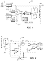
- Bidirektionale Niederspannungsstromversorgung "LVPS" (100), die Folgendes umfasst:einen ersten Stromrichter (120, 320), der dazu angeordnet ist, Strom von einer Eingangsstromquelle (110, 310) für eine Last bereitzustellen;einen zweiten Stromrichter, der dazu angeordnet ist, wahlweise Strom von der Last an einem Ausgang des ersten Stromrichters (120, 320) für die Eingabestromquelle (110. 310) zurückzugewinnen; undSteuerschaltung (140, 240, 340), die einen Einzelpulsweitenmodulator "PWM" (160) und Umschaltkreise (175, 275) umfasst, wobei die Umschaltkreise dazu ausgestaltet sind, entweder den ersten Stromrichter oder den zweiten Stromrichter zum Empfang der Ausgabe des PWM (160) auszuwählen, wobei die Steuerschaltung (140, 240, 340) ferner einen Fehlerverstärker (150, 250) umfasst, der die Stromquellenausgangsspannung (VO) und eine Referenzspannung (VREF) empfängt, einen Absolutwertschaltkreis (155), der dazu ausgestaltet ist, für den Pulsweitenmodulator (160) einen Absolutwert einer Differenz zwischen der Ausgabe des Fehlerverstärkers und null Volt bereitzustellen; und einen Konverterauswahlkomparator (170, 270), der mit dem Ausgang des Fehlerverstärkers verbunden ist und dazu ausgestaltet ist, den Umschaltkreis zu veranlassen, die Ausgabe des PWM (160) zwischen dem ersten Stromrichter (130, 230) und dem zweiten Stromrichter (110, 310) umzuschalten.
- Bidirektionale LVPS (100) nach Anspruch 1, wobei der Umschaltkreis dazu ausgestaltet ist, wahlweise entweder ein erstes Gate-Stellsignal für den ersten Stromrichter oder ein zweites Gate-Stellsignal für den zweiten Stromrichter bereitzustellen, um nur einen der Stromrichter zurzeit arbeiten zu lassen.
- Bidirektionale LVPS (100) nach Anspruch 2, die ferner umfasst:einen ersten Gate-Antriebskreis, um das erste Gate-Stellsignal bereitzustellen, um einen oder mehrere Konverterschalttransistoren des ersten Stromrichters zu betreiben; undeinen zweiten Gate-Antriebskreis, um ein zweites Gate-Stellsignal bereitzustellen, um einen oder mehrere Konverterschalttransistoren des zweiten Stromrichters zu betreiben;wobei der erste und der zweite Gate-Antriebskreis dazu ausgestaltet sind, eine Ausgabe von dem Umschaltkreis zu empfangen.
- Bidirektionale LVPS (100) nach Anspruch 2, wobei der Umschaltkreis dazu angeordnet ist, die LVPS (100) zu veranlassen, zwischen dem Betrieb des ersten Stromrichters, um Strom von der Eingangsstromquelle (110, 310) für die Last bereitzustellen, und dem Betrieb des zweiten Stromrichters, um Strom von der Last für die Eingangsstromquelle (110, 310) zurückzugewinnen, umzuschalten.
- Bidirektionale LVPS (100) nach Anspruch 5, wobei der Absolutwertschaltkreis dazu ausgestaltet ist, ein Signal in den PWM (160) bereitzustellen, das gleich der Differenz zwischen der Ausgabe des Fehlerverstärkers und null Volt ist; und
vorzugsweise,
wobei die bidirektionale LVPS (100) eine bidirektionale Motorantriebs-LVPS (100) ist, die dazu ausgestaltet ist, Strom für Motorantriebselektronik eines Motorantriebssystems bereitzustellen, und
wobei die Last die Motorantriebselektronik und einen Motor umfasst; und, vorzugsweise,
wobei der erste Stromrichter (120, 320) dazu ausgestaltet ist, Spannung für die Motorantriebselektronik zu regulieren, wenn der Motor sinkenden Strom aufweist, und
wobei der zweite Stromrichter dazu ausgestaltet ist, Spannung für die Motorantriebselektronik zu regulieren, wenn der Motor Strom der Energiequelle aufweist; und vorzugsweise,
wobei der Motor ein kryogener Kühlermotor ist. - Verfahren zum Betrieb einer bidirektionalen Niederspannungsstromversorgung "LVPS" (100), wobei das Verfahren Folgendes umfasst:Bereitstellen durch einen ersten Stromrichter (120, 320) von Strom von einer Eingangsstromquelle (110, 310) für eine Last;Wahlweises Zurückgewinnen durch einen zweiten Stromrichter von Strom von der Last am Ausgang des ersten Stromrichters (120, 320) für die Eingangsstromquelle (110, 310);Auswählen von entweder dem ersten Stromrichter (120, 320) oder dem zweiten Stromrichter (130, 330) zum Betrieb, um die Ausgabe eines Einzelpulsweitenmodulators (160) zu empfangen;Bereitstellen der Stromquellenausgangsspannung (VO) und einer Referenzspannung (VREF) für einen Fehlerverstärker (150; 250);Bereitstellen für den Pulsweitenmodulator (160) eines Absolutwerts einer Differenz zwischen der Ausgabe des Fehlerverstärkers (150, 250) und null Volt;Bereitstellen der Ausgabe des Fehlerverstärkers (150, 250) für einen Konverterauswahlkomparator (170, 270), der dazu ausgestaltet ist, einen Umschaltkreis (175, 275) zu veranlassen, die Ausgabe des Pulsweitenmodulators (160) zwischen dem ersten Stromrichter (130, 230) und dem zweiten Stromrichter (110, 310) umzuschalten.
- Verfahren nach Anspruch 6, das ferner Folgendes umfasst:
Wahlweises Bereitstellen von entweder einem ersten Gate-Stellsignal für den ersten Stromrichter (120, 320) oder von einem zweiten Gate-Stellsignal für den zweiten Stromrichter (130, 330), um nur einen Stromrichter zurzeit arbeiten zu lassen. - Verfahren nach Anspruch 7, das ferner Folgendes umfasst:Bereitstellen des ersten Gate-Stellsignals, um einen oder mehrere Konverterschalttransistoren des ersten Stromrichters (120, 320) zu betreiben; undBereitstellen eines zweiten Gate-Stellsignals, um einen oder mehrere Konverterschalttransistoren des zweiten Stromrichters (130, 330) zu betreiben.
- Verfahren nach Anspruch 7, wobei das wahlweise Bereitstellen die LVPS (100) dazu ausgestaltet, zwischen dem Betrieb des ersten Stromrichters (120, 320), um Strom von der Eingangsstromquelle (110, 310) für die Last bereitzustellen, und dem Betrieb des zweiten Stromrichters, um Strom von der Last für die Eingangsstromquelle zurückzugewinnen, umzuschalten.
- Verfahren nach Anspruch 9, das ferner Folgendes umfasst:Veranlassen des Umschaltkreises, eine Ausgabe des Pulsweitenmodulators zwischen dem ersten Stromrichter (120, 320) und dem zweiten Stromrichter (130, 330) umzuschalten, abhängig davon, ob die Last Energiequellen- oder sinkender Strom ist;oder vorzugsweise ferner umfassend das Bereitstellen eines Signals in den PWM (160), das gleich der Differenz zwischen der Ausgabe des Fehlerverstärkers und null Volt ist.
- Kryogenes Kühlersystem, das Folgendes umfasst:Motorantriebselektronik; undeinen bidirektionale Motorantrieb-Niederspannungsstromversorgung "LVPS" (100) nach Anspruch 1, die dazu ausgestaltet ist, Strom für die Motorantriebselektronik eines Motorantriebssystems bereitzustellen.
- Kryogenes Kühlersystem nach Anspruch 11, wobei der erste Stromrichter (120, 320) dazu ausgestaltet ist, Spannung für die Motorantriebselektronik zu regulieren, wenn der Motor sinkenden Strom aufweist, und wobei der zweite Stromrichter (130, 330) dazu ausgestaltet ist, die Spannung für die Motorantriebselektronik zu regulieren, wenn der Motor Strom der Energiequelle aufweist; und vorzugsweise
wobei der Umschaltkreis dazu ausgestaltet ist, wahlweise entweder ein erstes Gate-Stellsignal für den ersten Stromrichter (120, 320) oder ein zweites Gate-Stellsignal für den zweiten Stromrichter (130, 330) bereitzustellen, um zu veranlassen, dass nur einer der Stromrichter zurzeit arbeitet. - Ein nicht transitorisches computerlesbares Speichermedium, das Befehle zur Ausführung durch einen oder mehrere Prozessoren speichert, um eine bidirektionale Niederspannungs-Stromversorgung "LVPS" (100) dazu auszugestalten, Operationen durchzuführen, um:durch einen ersten Stromrichter (120, 320) Strom von einer Eingangsstromquelle (110, 310) für eine Last bereitzustellen;durch einen zweiten Stromrichter Strom von der Last bei einem Ausgang des ersten Stromrichters (120, 320) für die Eingabestromquelle (110, 310) wahlweise zurückzugewinnen;entweder den ersten Stromrichter (120, 320) oder den zweiten Stromrichter (130, 330) zum Betrieb auszuwählen, um die Ausgabe eines Einzelpulsweitenmodulators (160) zu empfangen;die Stromquellen-Ausgabespannung (VO) und eine Referenzspannung (VREF) für einen Fehlerverstärker (150, 250) bereitzustellen;für den Pulsweitenmodulator (160) einen Absolutwert einer Differenz zwischen der Ausgabe des Fehlerverstärkers (150, 250) und null Volt bereitzustellen;die Ausgabe des Fehlerverstärkers (150, 250) für einen Konverterauswahlkomparator (170, 270) bereitzustellen, der dazu ausgestaltet ist, den Umschaltkreis (175, 275) zu veranlassen, die Ausgabe des Pulsbreitenmodulators (160) zwischen dem ersten Stromrichter (130, 230) und dem zweiten Stromrichter (110, 310) umzuschalten.
- Das nicht transitorische computerlesbare Speichermedium nach Anspruch 13, wobei die Befehle ferner die bidirektionale LVPS (100) dazu ausgestalten, wahlweise entweder ein erstes Gate-Stellsignal für den ersten Stromrichter oder ein zweites Gate-Stellsignal für den zweiten Stromrichter bereitzustellen, um zu veranlassen, dass nur einer der Stromrichter zur Zeit arbeitet; und vorzugsweise
wobei die Befehle ferner die bidirektionale LVPS (100) dazu ausgestalten:das erste Gate-Stellsignal bereitzustellen, um einen oder mehrere Konverterumschalttransistor des ersten Stromrichters (120, 320) zu betreiben; undein zweites Gate-Antriebssignal bereitzustellen, um einen oder mehrere Konverterumschalttransistoren des zweiten Stromrichters (130, 330) zu betreiben; und vorzugsweisewobei das wahlweise Bereitstellen die LVPS (100) dazu ausgestaltet, zwischen dem Betrieb des ersten Stromrichters (120, 320), um Strom von der Eingangsstromquelle (110, 310) für die Last bereitzustellen, und dem Betrieb des zweiten Stromrichters (130, 330), um Strom von der Last für die Eingabestromquelle (110, 310) zurückzugewinnen, umzuschalten; und vorzugsweisewobei die Befehle ferner die bidirektionale LVPS (100) dazu ausgestalten:einen Absolutwert der Differenz zwischen einer Ausgabe eines Fehlerverstärkers und null Volt bereitzustellen; undden Umschaltkreis zu veranlassen, eine Ausgabe des Pulsweitenmodulators zwischen dem ersten Stromrichter (120, 320) und dem zweiten Stromrichter (130, 330) umzuschalten, abhängig davon, ob die Last Energiequellen- oder sinkender Strom ist; und vorzugweisewobei die Befehle ferner die bidirektionale LVPS (100) ausgestalten, ein Signal in den PWM (160) bereitzustellen, das gleich der Differenz zwischen der Ausgabe des Fehlerverstärkers und null Volt ist.
Applications Claiming Priority (3)
| Application Number | Priority Date | Filing Date | Title |
|---|---|---|---|
| US201462034889P | 2014-08-08 | 2014-08-08 | |
| US14/612,357 US9800129B2 (en) | 2014-08-08 | 2015-02-03 | Bidirectional low voltage power supply (LVPS) with single pulse width modulator (PWM), cryogenic cooler system, and method |
| PCT/US2015/044237 WO2016022932A1 (en) | 2014-08-08 | 2015-08-07 | Bidirectional low voltage power supply (lvps) with single pulse width modulator (pwm), cryogenic cooler system, and method |
Publications (2)
| Publication Number | Publication Date |
|---|---|
| EP3178158A1 EP3178158A1 (de) | 2017-06-14 |
| EP3178158B1 true EP3178158B1 (de) | 2018-12-26 |
Family
ID=53938401
Family Applications (1)
| Application Number | Title | Priority Date | Filing Date |
|---|---|---|---|
| EP15753807.5A Active EP3178158B1 (de) | 2014-08-08 | 2015-08-07 | Bidirektionale niederspannungsstromversorgung (lvps) mit einem einzelpulsbreitenmodulator (pwm), kryokühlsystem und verfahren |
Country Status (6)
| Country | Link |
|---|---|
| US (1) | US9800129B2 (de) |
| EP (1) | EP3178158B1 (de) |
| JP (1) | JP6251844B2 (de) |
| CA (1) | CA2956260C (de) |
| IL (1) | IL250142B (de) |
| WO (1) | WO2016022932A1 (de) |
Families Citing this family (7)
| Publication number | Priority date | Publication date | Assignee | Title |
|---|---|---|---|---|
| US9800129B2 (en) | 2014-08-08 | 2017-10-24 | Raytheon Company | Bidirectional low voltage power supply (LVPS) with single pulse width modulator (PWM), cryogenic cooler system, and method |
| US10236777B2 (en) | 2017-08-09 | 2019-03-19 | L3 Cincinnati Electronics Corporation | Magnetically isolated feedback circuits and regulated power supplies incorporating the same |
| CN107947534B (zh) * | 2017-12-01 | 2021-03-26 | 京东方科技集团股份有限公司 | 一种电源集成电路及其驱动方法、显示装置 |
| JP6647470B1 (ja) * | 2018-08-06 | 2020-02-14 | 三菱電機株式会社 | 電力変換装置 |
| US11165352B2 (en) | 2020-01-16 | 2021-11-02 | L3 Cincinnati Electronics Corporation | Capacitively isolated feedback circuits and regulated power supplies incorporating the same |
| KR20210141257A (ko) | 2020-05-15 | 2021-11-23 | 현대모비스 주식회사 | 카울크로스바 조립체 |
| KR102619173B1 (ko) | 2020-12-21 | 2024-01-03 | 현대모비스 주식회사 | 양방향 절연형 대용량 dc-dc 컨버터 및 그 제어방법 |
Citations (1)
| Publication number | Priority date | Publication date | Assignee | Title |
|---|---|---|---|---|
| US20080074095A1 (en) * | 2006-09-25 | 2008-03-27 | Telefus Mark D | Bi-directional regulator |
Family Cites Families (12)
| Publication number | Priority date | Publication date | Assignee | Title |
|---|---|---|---|---|
| US4481449A (en) * | 1982-09-17 | 1984-11-06 | Ampex Corporation | Power fail servo system |
| US5109185A (en) | 1989-09-29 | 1992-04-28 | Ball Newton E | Phase-controlled reversible power converter presenting a controllable counter emf to a source of an impressed voltage |
| US5428523A (en) | 1993-03-30 | 1995-06-27 | Ro Associates | Current sharing signal coupling/decoupling circuit for power converter systems |
| JP3627303B2 (ja) | 1995-08-11 | 2005-03-09 | 日立工機株式会社 | 遠心機 |
| US6771519B2 (en) * | 2000-09-29 | 2004-08-03 | Unison Industries, Inc. | Method and apparatus for generating high voltage |
| US8374011B2 (en) * | 2010-08-20 | 2013-02-12 | Magnetek, Inc. | Method and apparatus for boosting DC bus voltage |
| US8723490B2 (en) | 2010-08-30 | 2014-05-13 | Intersil Americas Inc. | Controlling a bidirectional DC-to-DC converter |
| JP2012152035A (ja) | 2011-01-19 | 2012-08-09 | Sharp Corp | 電気自動車充電装置、電気自動車充電方法、プログラムおよび記録媒体 |
| EP2506422B1 (de) | 2011-03-28 | 2019-02-13 | GE Energy Power Conversion Technology Limited | Schaltkreise für Gleichstrom-Energiespeicher |
| DE102011082730A1 (de) * | 2011-09-15 | 2013-03-21 | Robert Bosch Gmbh | Bidirektionaler Gleichspannungswandler |
| US9048720B2 (en) | 2013-04-02 | 2015-06-02 | Raytheon Company | Bidirectional motor driver low voltage power supply (LVPS) |
| US9800129B2 (en) | 2014-08-08 | 2017-10-24 | Raytheon Company | Bidirectional low voltage power supply (LVPS) with single pulse width modulator (PWM), cryogenic cooler system, and method |
-
2015
- 2015-02-03 US US14/612,357 patent/US9800129B2/en active Active
- 2015-08-07 WO PCT/US2015/044237 patent/WO2016022932A1/en active Application Filing
- 2015-08-07 EP EP15753807.5A patent/EP3178158B1/de active Active
- 2015-08-07 CA CA2956260A patent/CA2956260C/en active Active
- 2015-08-07 JP JP2017506913A patent/JP6251844B2/ja active Active
-
2017
- 2017-01-16 IL IL250142A patent/IL250142B/en active IP Right Grant
Patent Citations (1)
| Publication number | Priority date | Publication date | Assignee | Title |
|---|---|---|---|---|
| US20080074095A1 (en) * | 2006-09-25 | 2008-03-27 | Telefus Mark D | Bi-directional regulator |
Non-Patent Citations (2)
| Title |
|---|
| ANALOG DEVICES: "Buck or Boost, PWM Controller for Battery Test Solutions Data Sheet", 31 January 2014 (2014-01-31), XP055425669, Retrieved from the Internet <URL:http://www.gdcy.com/download_online.php?id=2018515&pdfid=2BF1FD8F66772F27006B1CDFDC4916A6&file=0510\adp1972_7747882.pdf> [retrieved on 20171116] * |
| ANALOG DEVICES: "In This Issue 2 Editor's Notes; New Product Introductions 3 Precision Resolver-to-Digital Converter Measures Angular Position and Velocity 9 Noise-Reduction Network for Adjustable-Output Low-Dropout Regulators 12 How to Stay Out of Deep Water when Designing with Bridge Sensors 15 Dual-Loop Clock Gen", 1 January 2014 (2014-01-01), XP055409119, Retrieved from the Internet <URL:http://www.analog.com/media/en/analog-dialogue/volume-48/number-1/articles/volume48-number1.pdf> [retrieved on 20170922] * |
Also Published As
| Publication number | Publication date |
|---|---|
| US20160043623A1 (en) | 2016-02-11 |
| JP2017524329A (ja) | 2017-08-24 |
| JP6251844B2 (ja) | 2017-12-20 |
| WO2016022932A1 (en) | 2016-02-11 |
| CA2956260C (en) | 2023-08-29 |
| IL250142B (en) | 2021-01-31 |
| US9800129B2 (en) | 2017-10-24 |
| IL250142A0 (en) | 2017-03-30 |
| EP3178158A1 (de) | 2017-06-14 |
| CA2956260A1 (en) | 2016-02-11 |
Similar Documents
| Publication | Publication Date | Title |
|---|---|---|
| EP3178158B1 (de) | Bidirektionale niederspannungsstromversorgung (lvps) mit einem einzelpulsbreitenmodulator (pwm), kryokühlsystem und verfahren | |
| CN109168326B (zh) | 电源装置 | |
| JP6394421B2 (ja) | 半導体スイッチング素子の駆動装置 | |
| US20160099564A1 (en) | Power delivery in a multiple-output system | |
| JP5597683B2 (ja) | 電源装置 | |
| US9490711B2 (en) | Gate drive power supply having gate drive voltage supply transformer circuits and kick starter circuit | |
| US20160141996A1 (en) | Electric motor system for vehicles and method of adjusting coil winding number of electric motor for vehicles | |
| KR20080037654A (ko) | 집적 이상 다이오드 기능의 듀얼 입력 dc-dc 변환기 | |
| JP4597815B2 (ja) | 電圧制御装置 | |
| KR20160053976A (ko) | 단일 제어 루프를 갖는 다중-출력 부스트 레귤레이터 | |
| US11121631B2 (en) | DC-DC converter | |
| CN111835199A (zh) | 用于下一代低功率汽车系统的自适应高效待机电源方案 | |
| EP3316274B1 (de) | Treiberschaltung zum betrieb eines relais | |
| JP2011229011A (ja) | スイッチングトランジスタの制御回路およびそれを用いた電力変換装置 | |
| US20100219787A1 (en) | Motor drive system for driving motor provided with a plurality of windings | |
| US20190173383A1 (en) | Buck-boost converter power supply with drive circuit | |
| US20200358359A1 (en) | Method and apparatus for controlling a dc/dc power converter | |
| US20160118883A1 (en) | Simo (single inductor multiple output) bidirectional dual-boost architecture | |
| JP2008086173A (ja) | 半導体集積回路とこれを使用した多出力電源装置 | |
| EP3098074A1 (de) | Steuerungsvorrichtung und steuerungsverfahren dafür | |
| JP5460562B2 (ja) | Dc−dcコンバータ及びその制御方法 | |
| JP6475170B2 (ja) | 電源システム及びその制御方法 | |
| CN109643952B (zh) | Dc/dc转换器 | |
| US20230344348A1 (en) | Universal buck-boost topology with an active negative holdup voltage | |
| US20230344349A1 (en) | Universal buck-boost topology with an active positive holdup voltage |
Legal Events
| Date | Code | Title | Description |
|---|---|---|---|
| STAA | Information on the status of an ep patent application or granted ep patent |
Free format text: STATUS: THE INTERNATIONAL PUBLICATION HAS BEEN MADE |
|
| PUAI | Public reference made under article 153(3) epc to a published international application that has entered the european phase |
Free format text: ORIGINAL CODE: 0009012 |
|
| STAA | Information on the status of an ep patent application or granted ep patent |
Free format text: STATUS: REQUEST FOR EXAMINATION WAS MADE |
|
| 17P | Request for examination filed |
Effective date: 20170125 |
|
| AK | Designated contracting states |
Kind code of ref document: A1 Designated state(s): AL AT BE BG CH CY CZ DE DK EE ES FI FR GB GR HR HU IE IS IT LI LT LU LV MC MK MT NL NO PL PT RO RS SE SI SK SM TR |
|
| AX | Request for extension of the european patent |
Extension state: BA ME |
|
| DAV | Request for validation of the european patent (deleted) | ||
| DAX | Request for extension of the european patent (deleted) | ||
| STAA | Information on the status of an ep patent application or granted ep patent |
Free format text: STATUS: EXAMINATION IS IN PROGRESS |
|
| 17Q | First examination report despatched |
Effective date: 20171122 |
|
| GRAP | Despatch of communication of intention to grant a patent |
Free format text: ORIGINAL CODE: EPIDOSNIGR1 |
|
| STAA | Information on the status of an ep patent application or granted ep patent |
Free format text: STATUS: GRANT OF PATENT IS INTENDED |
|
| INTG | Intention to grant announced |
Effective date: 20180718 |
|
| GRAS | Grant fee paid |
Free format text: ORIGINAL CODE: EPIDOSNIGR3 |
|
| GRAA | (expected) grant |
Free format text: ORIGINAL CODE: 0009210 |
|
| STAA | Information on the status of an ep patent application or granted ep patent |
Free format text: STATUS: THE PATENT HAS BEEN GRANTED |
|
| AK | Designated contracting states |
Kind code of ref document: B1 Designated state(s): AL AT BE BG CH CY CZ DE DK EE ES FI FR GB GR HR HU IE IS IT LI LT LU LV MC MK MT NL NO PL PT RO RS SE SI SK SM TR |
|
| REG | Reference to a national code |
Ref country code: GB Ref legal event code: FG4D |
|
| REG | Reference to a national code |
Ref country code: CH Ref legal event code: EP |
|
| REG | Reference to a national code |
Ref country code: AT Ref legal event code: REF Ref document number: 1082794 Country of ref document: AT Kind code of ref document: T Effective date: 20190115 |
|
| REG | Reference to a national code |
Ref country code: DE Ref legal event code: R096 Ref document number: 602015022343 Country of ref document: DE |
|
| REG | Reference to a national code |
Ref country code: IE Ref legal event code: FG4D |
|
| PG25 | Lapsed in a contracting state [announced via postgrant information from national office to epo] |
Ref country code: NO Free format text: LAPSE BECAUSE OF FAILURE TO SUBMIT A TRANSLATION OF THE DESCRIPTION OR TO PAY THE FEE WITHIN THE PRESCRIBED TIME-LIMIT Effective date: 20190326 Ref country code: HR Free format text: LAPSE BECAUSE OF FAILURE TO SUBMIT A TRANSLATION OF THE DESCRIPTION OR TO PAY THE FEE WITHIN THE PRESCRIBED TIME-LIMIT Effective date: 20181226 Ref country code: LT Free format text: LAPSE BECAUSE OF FAILURE TO SUBMIT A TRANSLATION OF THE DESCRIPTION OR TO PAY THE FEE WITHIN THE PRESCRIBED TIME-LIMIT Effective date: 20181226 Ref country code: BG Free format text: LAPSE BECAUSE OF FAILURE TO SUBMIT A TRANSLATION OF THE DESCRIPTION OR TO PAY THE FEE WITHIN THE PRESCRIBED TIME-LIMIT Effective date: 20190326 Ref country code: FI Free format text: LAPSE BECAUSE OF FAILURE TO SUBMIT A TRANSLATION OF THE DESCRIPTION OR TO PAY THE FEE WITHIN THE PRESCRIBED TIME-LIMIT Effective date: 20181226 Ref country code: LV Free format text: LAPSE BECAUSE OF FAILURE TO SUBMIT A TRANSLATION OF THE DESCRIPTION OR TO PAY THE FEE WITHIN THE PRESCRIBED TIME-LIMIT Effective date: 20181226 |
|
| REG | Reference to a national code |
Ref country code: NL Ref legal event code: MP Effective date: 20181226 |
|
| REG | Reference to a national code |
Ref country code: LT Ref legal event code: MG4D |
|
| PG25 | Lapsed in a contracting state [announced via postgrant information from national office to epo] |
Ref country code: AL Free format text: LAPSE BECAUSE OF FAILURE TO SUBMIT A TRANSLATION OF THE DESCRIPTION OR TO PAY THE FEE WITHIN THE PRESCRIBED TIME-LIMIT Effective date: 20181226 Ref country code: SE Free format text: LAPSE BECAUSE OF FAILURE TO SUBMIT A TRANSLATION OF THE DESCRIPTION OR TO PAY THE FEE WITHIN THE PRESCRIBED TIME-LIMIT Effective date: 20181226 Ref country code: RS Free format text: LAPSE BECAUSE OF FAILURE TO SUBMIT A TRANSLATION OF THE DESCRIPTION OR TO PAY THE FEE WITHIN THE PRESCRIBED TIME-LIMIT Effective date: 20181226 Ref country code: GR Free format text: LAPSE BECAUSE OF FAILURE TO SUBMIT A TRANSLATION OF THE DESCRIPTION OR TO PAY THE FEE WITHIN THE PRESCRIBED TIME-LIMIT Effective date: 20190327 |
|
| REG | Reference to a national code |
Ref country code: AT Ref legal event code: MK05 Ref document number: 1082794 Country of ref document: AT Kind code of ref document: T Effective date: 20181226 |
|
| PG25 | Lapsed in a contracting state [announced via postgrant information from national office to epo] |
Ref country code: NL Free format text: LAPSE BECAUSE OF FAILURE TO SUBMIT A TRANSLATION OF THE DESCRIPTION OR TO PAY THE FEE WITHIN THE PRESCRIBED TIME-LIMIT Effective date: 20181226 |
|
| PG25 | Lapsed in a contracting state [announced via postgrant information from national office to epo] |
Ref country code: CZ Free format text: LAPSE BECAUSE OF FAILURE TO SUBMIT A TRANSLATION OF THE DESCRIPTION OR TO PAY THE FEE WITHIN THE PRESCRIBED TIME-LIMIT Effective date: 20181226 Ref country code: IT Free format text: LAPSE BECAUSE OF FAILURE TO SUBMIT A TRANSLATION OF THE DESCRIPTION OR TO PAY THE FEE WITHIN THE PRESCRIBED TIME-LIMIT Effective date: 20181226 Ref country code: PL Free format text: LAPSE BECAUSE OF FAILURE TO SUBMIT A TRANSLATION OF THE DESCRIPTION OR TO PAY THE FEE WITHIN THE PRESCRIBED TIME-LIMIT Effective date: 20181226 Ref country code: ES Free format text: LAPSE BECAUSE OF FAILURE TO SUBMIT A TRANSLATION OF THE DESCRIPTION OR TO PAY THE FEE WITHIN THE PRESCRIBED TIME-LIMIT Effective date: 20181226 Ref country code: PT Free format text: LAPSE BECAUSE OF FAILURE TO SUBMIT A TRANSLATION OF THE DESCRIPTION OR TO PAY THE FEE WITHIN THE PRESCRIBED TIME-LIMIT Effective date: 20190426 |
|
| PG25 | Lapsed in a contracting state [announced via postgrant information from national office to epo] |
Ref country code: EE Free format text: LAPSE BECAUSE OF FAILURE TO SUBMIT A TRANSLATION OF THE DESCRIPTION OR TO PAY THE FEE WITHIN THE PRESCRIBED TIME-LIMIT Effective date: 20181226 Ref country code: SM Free format text: LAPSE BECAUSE OF FAILURE TO SUBMIT A TRANSLATION OF THE DESCRIPTION OR TO PAY THE FEE WITHIN THE PRESCRIBED TIME-LIMIT Effective date: 20181226 Ref country code: IS Free format text: LAPSE BECAUSE OF FAILURE TO SUBMIT A TRANSLATION OF THE DESCRIPTION OR TO PAY THE FEE WITHIN THE PRESCRIBED TIME-LIMIT Effective date: 20190426 Ref country code: RO Free format text: LAPSE BECAUSE OF FAILURE TO SUBMIT A TRANSLATION OF THE DESCRIPTION OR TO PAY THE FEE WITHIN THE PRESCRIBED TIME-LIMIT Effective date: 20181226 Ref country code: SK Free format text: LAPSE BECAUSE OF FAILURE TO SUBMIT A TRANSLATION OF THE DESCRIPTION OR TO PAY THE FEE WITHIN THE PRESCRIBED TIME-LIMIT Effective date: 20181226 |
|
| REG | Reference to a national code |
Ref country code: DE Ref legal event code: R097 Ref document number: 602015022343 Country of ref document: DE |
|
| PG25 | Lapsed in a contracting state [announced via postgrant information from national office to epo] |
Ref country code: AT Free format text: LAPSE BECAUSE OF FAILURE TO SUBMIT A TRANSLATION OF THE DESCRIPTION OR TO PAY THE FEE WITHIN THE PRESCRIBED TIME-LIMIT Effective date: 20181226 Ref country code: DK Free format text: LAPSE BECAUSE OF FAILURE TO SUBMIT A TRANSLATION OF THE DESCRIPTION OR TO PAY THE FEE WITHIN THE PRESCRIBED TIME-LIMIT Effective date: 20181226 |
|
| PLBE | No opposition filed within time limit |
Free format text: ORIGINAL CODE: 0009261 |
|
| STAA | Information on the status of an ep patent application or granted ep patent |
Free format text: STATUS: NO OPPOSITION FILED WITHIN TIME LIMIT |
|
| 26N | No opposition filed |
Effective date: 20190927 |
|
| PG25 | Lapsed in a contracting state [announced via postgrant information from national office to epo] |
Ref country code: SI Free format text: LAPSE BECAUSE OF FAILURE TO SUBMIT A TRANSLATION OF THE DESCRIPTION OR TO PAY THE FEE WITHIN THE PRESCRIBED TIME-LIMIT Effective date: 20181226 |
|
| PG25 | Lapsed in a contracting state [announced via postgrant information from national office to epo] |
Ref country code: TR Free format text: LAPSE BECAUSE OF FAILURE TO SUBMIT A TRANSLATION OF THE DESCRIPTION OR TO PAY THE FEE WITHIN THE PRESCRIBED TIME-LIMIT Effective date: 20181226 |
|
| PG25 | Lapsed in a contracting state [announced via postgrant information from national office to epo] |
Ref country code: CH Free format text: LAPSE BECAUSE OF NON-PAYMENT OF DUE FEES Effective date: 20190831 Ref country code: LU Free format text: LAPSE BECAUSE OF NON-PAYMENT OF DUE FEES Effective date: 20190807 Ref country code: LI Free format text: LAPSE BECAUSE OF NON-PAYMENT OF DUE FEES Effective date: 20190831 Ref country code: MC Free format text: LAPSE BECAUSE OF FAILURE TO SUBMIT A TRANSLATION OF THE DESCRIPTION OR TO PAY THE FEE WITHIN THE PRESCRIBED TIME-LIMIT Effective date: 20181226 |
|
| REG | Reference to a national code |
Ref country code: BE Ref legal event code: MM Effective date: 20190831 |
|
| PG25 | Lapsed in a contracting state [announced via postgrant information from national office to epo] |
Ref country code: IE Free format text: LAPSE BECAUSE OF NON-PAYMENT OF DUE FEES Effective date: 20190807 |
|
| PG25 | Lapsed in a contracting state [announced via postgrant information from national office to epo] |
Ref country code: BE Free format text: LAPSE BECAUSE OF NON-PAYMENT OF DUE FEES Effective date: 20190831 |
|
| PG25 | Lapsed in a contracting state [announced via postgrant information from national office to epo] |
Ref country code: CY Free format text: LAPSE BECAUSE OF FAILURE TO SUBMIT A TRANSLATION OF THE DESCRIPTION OR TO PAY THE FEE WITHIN THE PRESCRIBED TIME-LIMIT Effective date: 20181226 |
|
| PG25 | Lapsed in a contracting state [announced via postgrant information from national office to epo] |
Ref country code: MT Free format text: LAPSE BECAUSE OF FAILURE TO SUBMIT A TRANSLATION OF THE DESCRIPTION OR TO PAY THE FEE WITHIN THE PRESCRIBED TIME-LIMIT Effective date: 20181226 Ref country code: HU Free format text: LAPSE BECAUSE OF FAILURE TO SUBMIT A TRANSLATION OF THE DESCRIPTION OR TO PAY THE FEE WITHIN THE PRESCRIBED TIME-LIMIT; INVALID AB INITIO Effective date: 20150807 |
|
| PG25 | Lapsed in a contracting state [announced via postgrant information from national office to epo] |
Ref country code: MK Free format text: LAPSE BECAUSE OF FAILURE TO SUBMIT A TRANSLATION OF THE DESCRIPTION OR TO PAY THE FEE WITHIN THE PRESCRIBED TIME-LIMIT Effective date: 20181226 |
|
| P01 | Opt-out of the competence of the unified patent court (upc) registered |
Effective date: 20230530 |
|
| PGFP | Annual fee paid to national office [announced via postgrant information from national office to epo] |
Ref country code: GB Payment date: 20230720 Year of fee payment: 9 |
|
| PGFP | Annual fee paid to national office [announced via postgrant information from national office to epo] |
Ref country code: FR Payment date: 20230720 Year of fee payment: 9 Ref country code: DE Payment date: 20230720 Year of fee payment: 9 |