EP3178158B1 - Bidirectional low voltage power supply (lvps) with single pulse width modulator (pwm), cryogenic cooler system, and method - Google Patents
Bidirectional low voltage power supply (lvps) with single pulse width modulator (pwm), cryogenic cooler system, and method Download PDFInfo
- Publication number
- EP3178158B1 EP3178158B1 EP15753807.5A EP15753807A EP3178158B1 EP 3178158 B1 EP3178158 B1 EP 3178158B1 EP 15753807 A EP15753807 A EP 15753807A EP 3178158 B1 EP3178158 B1 EP 3178158B1
- Authority
- EP
- European Patent Office
- Prior art keywords
- power
- power converter
- converter
- output
- lvps
- Prior art date
- Legal status (The legal status is an assumption and is not a legal conclusion. Google has not performed a legal analysis and makes no representation as to the accuracy of the status listed.)
- Active
Links
- 230000002457 bidirectional effect Effects 0.000 title claims description 43
- 238000000034 method Methods 0.000 title claims description 14
- 238000012358 sourcing Methods 0.000 claims description 8
- 238000004064 recycling Methods 0.000 claims description 3
- 238000010586 diagram Methods 0.000 description 2
- 238000003491 array Methods 0.000 description 1
- 230000001276 controlling effect Effects 0.000 description 1
- 238000007796 conventional method Methods 0.000 description 1
- 230000006870 function Effects 0.000 description 1
- 230000003287 optical effect Effects 0.000 description 1
- 230000001105 regulatory effect Effects 0.000 description 1
- 239000012085 test solution Substances 0.000 description 1
Images

Classifications
-
- H—ELECTRICITY
- H02—GENERATION; CONVERSION OR DISTRIBUTION OF ELECTRIC POWER
- H02M—APPARATUS FOR CONVERSION BETWEEN AC AND AC, BETWEEN AC AND DC, OR BETWEEN DC AND DC, AND FOR USE WITH MAINS OR SIMILAR POWER SUPPLY SYSTEMS; CONVERSION OF DC OR AC INPUT POWER INTO SURGE OUTPUT POWER; CONTROL OR REGULATION THEREOF
- H02M3/00—Conversion of dc power input into dc power output
- H02M3/22—Conversion of dc power input into dc power output with intermediate conversion into ac
- H02M3/24—Conversion of dc power input into dc power output with intermediate conversion into ac by static converters
- H02M3/28—Conversion of dc power input into dc power output with intermediate conversion into ac by static converters using discharge tubes with control electrode or semiconductor devices with control electrode to produce the intermediate ac
- H02M3/325—Conversion of dc power input into dc power output with intermediate conversion into ac by static converters using discharge tubes with control electrode or semiconductor devices with control electrode to produce the intermediate ac using devices of a triode or a transistor type requiring continuous application of a control signal
- H02M3/335—Conversion of dc power input into dc power output with intermediate conversion into ac by static converters using discharge tubes with control electrode or semiconductor devices with control electrode to produce the intermediate ac using devices of a triode or a transistor type requiring continuous application of a control signal using semiconductor devices only
- H02M3/33538—Conversion of dc power input into dc power output with intermediate conversion into ac by static converters using discharge tubes with control electrode or semiconductor devices with control electrode to produce the intermediate ac using devices of a triode or a transistor type requiring continuous application of a control signal using semiconductor devices only of the forward type
- H02M3/33546—Conversion of dc power input into dc power output with intermediate conversion into ac by static converters using discharge tubes with control electrode or semiconductor devices with control electrode to produce the intermediate ac using devices of a triode or a transistor type requiring continuous application of a control signal using semiconductor devices only of the forward type with automatic control of the output voltage or current
- H02M3/33553—Conversion of dc power input into dc power output with intermediate conversion into ac by static converters using discharge tubes with control electrode or semiconductor devices with control electrode to produce the intermediate ac using devices of a triode or a transistor type requiring continuous application of a control signal using semiconductor devices only of the forward type with automatic control of the output voltage or current with galvanic isolation between input and output of both the power stage and the feedback loop
-
- H—ELECTRICITY
- H02—GENERATION; CONVERSION OR DISTRIBUTION OF ELECTRIC POWER
- H02M—APPARATUS FOR CONVERSION BETWEEN AC AND AC, BETWEEN AC AND DC, OR BETWEEN DC AND DC, AND FOR USE WITH MAINS OR SIMILAR POWER SUPPLY SYSTEMS; CONVERSION OF DC OR AC INPUT POWER INTO SURGE OUTPUT POWER; CONTROL OR REGULATION THEREOF
- H02M3/00—Conversion of dc power input into dc power output
- H02M3/22—Conversion of dc power input into dc power output with intermediate conversion into ac
- H02M3/24—Conversion of dc power input into dc power output with intermediate conversion into ac by static converters
- H02M3/28—Conversion of dc power input into dc power output with intermediate conversion into ac by static converters using discharge tubes with control electrode or semiconductor devices with control electrode to produce the intermediate ac
- H02M3/285—Single converters with a plurality of output stages connected in parallel
-
- H—ELECTRICITY
- H02—GENERATION; CONVERSION OR DISTRIBUTION OF ELECTRIC POWER
- H02M—APPARATUS FOR CONVERSION BETWEEN AC AND AC, BETWEEN AC AND DC, OR BETWEEN DC AND DC, AND FOR USE WITH MAINS OR SIMILAR POWER SUPPLY SYSTEMS; CONVERSION OF DC OR AC INPUT POWER INTO SURGE OUTPUT POWER; CONTROL OR REGULATION THEREOF
- H02M3/00—Conversion of dc power input into dc power output
- H02M3/22—Conversion of dc power input into dc power output with intermediate conversion into ac
- H02M3/24—Conversion of dc power input into dc power output with intermediate conversion into ac by static converters
- H02M3/28—Conversion of dc power input into dc power output with intermediate conversion into ac by static converters using discharge tubes with control electrode or semiconductor devices with control electrode to produce the intermediate ac
- H02M3/325—Conversion of dc power input into dc power output with intermediate conversion into ac by static converters using discharge tubes with control electrode or semiconductor devices with control electrode to produce the intermediate ac using devices of a triode or a transistor type requiring continuous application of a control signal
- H02M3/335—Conversion of dc power input into dc power output with intermediate conversion into ac by static converters using discharge tubes with control electrode or semiconductor devices with control electrode to produce the intermediate ac using devices of a triode or a transistor type requiring continuous application of a control signal using semiconductor devices only
- H02M3/33507—Conversion of dc power input into dc power output with intermediate conversion into ac by static converters using discharge tubes with control electrode or semiconductor devices with control electrode to produce the intermediate ac using devices of a triode or a transistor type requiring continuous application of a control signal using semiconductor devices only with automatic control of the output voltage or current, e.g. flyback converters
- H02M3/33523—Conversion of dc power input into dc power output with intermediate conversion into ac by static converters using discharge tubes with control electrode or semiconductor devices with control electrode to produce the intermediate ac using devices of a triode or a transistor type requiring continuous application of a control signal using semiconductor devices only with automatic control of the output voltage or current, e.g. flyback converters with galvanic isolation between input and output of both the power stage and the feedback loop
-
- H—ELECTRICITY
- H02—GENERATION; CONVERSION OR DISTRIBUTION OF ELECTRIC POWER
- H02M—APPARATUS FOR CONVERSION BETWEEN AC AND AC, BETWEEN AC AND DC, OR BETWEEN DC AND DC, AND FOR USE WITH MAINS OR SIMILAR POWER SUPPLY SYSTEMS; CONVERSION OF DC OR AC INPUT POWER INTO SURGE OUTPUT POWER; CONTROL OR REGULATION THEREOF
- H02M3/00—Conversion of dc power input into dc power output
- H02M3/22—Conversion of dc power input into dc power output with intermediate conversion into ac
- H02M3/24—Conversion of dc power input into dc power output with intermediate conversion into ac by static converters
- H02M3/28—Conversion of dc power input into dc power output with intermediate conversion into ac by static converters using discharge tubes with control electrode or semiconductor devices with control electrode to produce the intermediate ac
- H02M3/325—Conversion of dc power input into dc power output with intermediate conversion into ac by static converters using discharge tubes with control electrode or semiconductor devices with control electrode to produce the intermediate ac using devices of a triode or a transistor type requiring continuous application of a control signal
- H02M3/335—Conversion of dc power input into dc power output with intermediate conversion into ac by static converters using discharge tubes with control electrode or semiconductor devices with control electrode to produce the intermediate ac using devices of a triode or a transistor type requiring continuous application of a control signal using semiconductor devices only
- H02M3/33569—Conversion of dc power input into dc power output with intermediate conversion into ac by static converters using discharge tubes with control electrode or semiconductor devices with control electrode to produce the intermediate ac using devices of a triode or a transistor type requiring continuous application of a control signal using semiconductor devices only having several active switching elements
- H02M3/33576—Conversion of dc power input into dc power output with intermediate conversion into ac by static converters using discharge tubes with control electrode or semiconductor devices with control electrode to produce the intermediate ac using devices of a triode or a transistor type requiring continuous application of a control signal using semiconductor devices only having several active switching elements having at least one active switching element at the secondary side of an isolation transformer
- H02M3/33584—Bidirectional converters
-
- H—ELECTRICITY
- H02—GENERATION; CONVERSION OR DISTRIBUTION OF ELECTRIC POWER
- H02M—APPARATUS FOR CONVERSION BETWEEN AC AND AC, BETWEEN AC AND DC, OR BETWEEN DC AND DC, AND FOR USE WITH MAINS OR SIMILAR POWER SUPPLY SYSTEMS; CONVERSION OF DC OR AC INPUT POWER INTO SURGE OUTPUT POWER; CONTROL OR REGULATION THEREOF
- H02M1/00—Details of apparatus for conversion
- H02M1/0067—Converter structures employing plural converter units, other than for parallel operation of the units on a single load
-
- H—ELECTRICITY
- H02—GENERATION; CONVERSION OR DISTRIBUTION OF ELECTRIC POWER
- H02M—APPARATUS FOR CONVERSION BETWEEN AC AND AC, BETWEEN AC AND DC, OR BETWEEN DC AND DC, AND FOR USE WITH MAINS OR SIMILAR POWER SUPPLY SYSTEMS; CONVERSION OF DC OR AC INPUT POWER INTO SURGE OUTPUT POWER; CONTROL OR REGULATION THEREOF
- H02M1/00—Details of apparatus for conversion
- H02M1/0095—Hybrid converter topologies, e.g. NPC mixed with flying capacitor, thyristor converter mixed with MMC or charge pump mixed with buck
Description
- Embodiments pertain to power sources and power supplies. Some embodiments relate to bidirectional low voltage power supplies. Some embodiments relate to cryogenic cooler systems. Some embodiments relate to motor systems, motor drive electronics and motors.
- Some motor applications, such as cryogenic cooler motors, can act as power sources during certain operating conditions and in some part of their operating cycle. The motor drive electronics may be configured to sink power from the motor as well as source power to the motor. Historically, power sourced from cryocooler motors has been dissipated.
- Thus there are general needs for more efficient motor systems including cryogenic cooler systems. There are also general needs for more efficient power supplies suitable for systems, such as motor drive systems and cryogenic cooler systems.
-
US5726550 provides a motor control system for controlling power supplied to an electric motor rotating a rotor employed in a centrifuge. -
US2013/278213 provides a control apparatus of an electric vehicle charging apparatus applies control such that, when not charging a motive power storage battery, a storage battery for supplying charging power is charged with electric power supplied from an alternating current power source input. - Documents : Analog Devices: "Buck or Boost, PWM Controller for Battery Test Solutions Data Sheet" and
US2008/074095 are prior art to the present application. - According to an aspect of the present invention, there is provided a bidirectional low voltage power supply 'LVPS' comprising: a first power converter arranged to provide power from an input power source to a load; a second power converter arranged to selectively recycle power from the load at an output of the first converter back to the input power source; and control circuitry comprising a single pulse width modulator 'PWM' and switching circuitry, the switching circuitry configured to select either the first power converter or the second power converter for reception of an output of the PWM, the control circuitry further comprising an error amplifier, an absolute value circuit configured to provide an absolute value of a difference between an output of an error amplifier and zero volts; and a converter selection comparator configured to cause the switching circuitry to switch an output of the PWM between the first power converter and the second power converter.
- According to another aspect of the present invention, there is provided a method for operation of a bidirectional low voltage power supply 'LVPS', the method comprising: providing, by a first power converter, power from an input power source to a load; selectively recycling, by a second power converter, power from the load at an output of the first power converter back to the input power source; and selecting either the first power converter or the second power converter for operation to receive an output of a single pulse width modulator; providing an absolute value of a difference between an output of an error amplifier and zero volts; and switching an output of the pulse width modulator between the first power converter and the second power converter.
- According to another aspect of the present invention, there is provided a non-transitory computer-readable storage medium that stores instructions for execution by one or more processors to configure a bidirectional low voltage power supply 'LVPS' to perform operations to: provide, by a first power converter, power from an input power source to a load; selectively recycle, by a second power converter, power from the load at an output of the first power converter back to the input power source; and select either the first power converter or the second power converter for operation to receive an output of a single pulse width modulator; provide an absolute value of a difference between an output of an error amplifier and zero volts; and switch an output of the pulse width modulator between the first power converter and the second power converter.
-
-
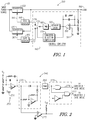
FIG. 1 is a functional diagram of a bidirectional low voltage power supply (LVPS) in accordance with some embodiments; -
FIG. 2 illustrates control circuitry in accordance with some embodiments; -
FIG. 3 illustrates a bidirectional low voltage power supply in accordance with some embodiments; and -
FIG. 4 illustrates a procedure for bidirectional low-voltage power supply operation in accordance with some embodiments. - The following description and the drawings sufficiently illustrate specific embodiments to enable those skilled in the art to practice them. Other embodiments may incorporate structural, logical, electrical, process, and other changes. Portions and features of some embodiments may be included in, or substituted for, those of other embodiments. Embodiments set forth in the claims encompass all available equivalents of those claims.
-
FIG. 1 is a functional diagram of a bidirectional low voltage power supply (LVPS) in accordance with some embodiments. The bidirectional low voltage power supply (LVPS) 100 may include a first converter 120 arranged to provide power from aninput power source 110 to aload 190, and a second converter 130 arranged to selectively recycle power from theload 190 at an output of the first converter 120 back to theinput power source 110. The bidirectional low voltage power supply100 may also includecontrol circuitry 140. The control circuitry may include, among other things, a single pulse width modulator (PWM) 160 andswitching circuitry 175. Theswitching circuitry 175 may be configured to select either the first power converter 120 or the second power converter 130 for reception of the output of thePWM 160. - In these embodiments, the single
bidirectional LVPS 100 may be used to power theload 190 and recycle power returned from theload 190 back to theinput power source 110. This may increase system efficiency and may reduce the thermal load. Unlike some conventional systems, the single PWM 160 is used to control both converters (i.e., converter 120 and converter 130). An example of a bidirectional LVPS that uses two separate converters with each converter having a PWM is described inU.S. Patent Application Serial No 13/855,295 [ref no. 12-2965] which is assigned to the same assignee as the present application - In some embodiments, the
switching circuitry 175 may be configured to selectively provide either a first gate drive signal 176 to the first power converter 120 or a secondgate drive signal 177 to the second power converter 130 to cause only one of the power converters 120 or 130 to operate at any one time. In these embodiments, the first converter 120 may be configured to regulate voltage to theload 190 when theload 190 is sinking power and the second converter 130 may be configured to regulate voltage to theload 190 when the load is sourcing power. In some motor drive and cryogenic cooler embodiments, the first converter 120 is configured to regulate voltage to motor drive electronics when a motor is sinking power, and the second converter 130 is configured to regulate voltage to the motor drive electronics when the motor is sourcing power, although the scope of the embodiments is not limited in this respect. - In some embodiments, a first
gate drive circuit 180 may be configured to provide agate drive signal 182 to drive one or more converter switch transistors of the first power converter 120. A secondgate drive circuit 185 may be configured to provide agate drive signal 187 to drive one or more converter switch transistors of the second power converter 130. In some embodiments, the firstgate drive circuit 180 and/or the secondgate drive circuit 185 may be isolated gate drives, although the scope of the embodiments is not limited in this respect. - In some embodiments, the
switching circuitry 175 may be arranged to cause theLVPS 100 to switch between operation of the first power converter 120 to provide power from theinput power source 110 to theload 190 and operation of the second power converter 130 to recycle power from theload 190 back to theinput power source 110. In some embodiments, theinput power source 110 may be an input power bus, although the scope of the embodiments is not limited in this respect. - In some embodiments, the
control circuitry 140 may also comprise anerror amplifier 150, anabsolute value circuit 155 and aconverter selection comparator 170. In these embodiments, theabsolute value circuit 155 may be configured to provide the absolute value of the difference between the output voltage of theerror amplifier 150 and zero volts. Theconverter selection comparator 170 may be configured to cause theswitching circuitry 175 to switch an output of thepulse width modulator 160 between the first power converter 120 and the second power converter 130. In some of these embodiments, the regulated power supply output voltage and thereference voltage 151 may be any suitable positive voltage, although the scope of the embodiments is not limited in this respect as other output voltages and reference voltages may be used. In some embodiments, theabsolute value circuit 155 may be configured to provide a signal into thePWM 160 equal to the difference between the output of theerror amplifier 150 and a second reference voltage. - The
control circuitry 140 illustrated inFIG. 1 is provided as an example configuration. Other configurations for thecontrol circuitry 140 may also be suitable for use in thebidirectional LVPS 100. - In some embodiments, the
bidirectional LVPS 100 may be a bidirectional motor driver LVPS configured to provide power to motor drive electronics of a motor drive system. In these embodiments, theload 190 may comprise the motor drive electronics and the motor, although the scope of the embodiments is not limited in this respect. In some embodiments, the first converter 120 may be configured to regulate voltage to the motor drive electronics when the motor is sinking power and the second converter 130 may be configured to regulate voltage to the motor drive electronics when the motor is sourcing power. In some embodiments, the motor may be a cryogenic cooler motor, although the scope of the embodiments is not limited in this respect. In some example embodiments, thebidirectional LVPS 100 may save up to 20 Watts or more over some conventional techniques which provides a significant improvement in efficiency. - * Some embodiments are directed to a cryogenic cooler system. In these embodiments, the cryogenic cooler system may include motor drive electronics and a bidirectional motor driver LVPS 100 configured to provide power to the motor drive electronics of a motor drive system. In these embodiments, the bidirectional motor drive LVPS may comprise a first converter 120 arranged to provide power from an
input power source 110 to a load comprising the motor drive electronics and a motor, a second converter 130 arranged to selectively recycle power from theload 190 at an output of the first converter 120 back to theinput power source 110, andcontrol circuitry 140 comprising asingle PWM 160 andswitching circuitry 175. In some embodiments, theswitching circuitry 175 may be configured to select either the first power converter 120 or the second power converter 130 for reception of an output of thePWM 160. - In some of these cryogenic cooler system embodiments, the first converter 120 may be configured to regulate voltage to the motor drive electronics when the motor is sinking power and the second converter 130 may be configured to regulate voltage to the motor drive electronics when the motor is sourcing power, although the scope of the embodiments is not limited in this respect. In some of these cryogenic cooler system embodiments, the
switching circuitry 175 may be configured to selectively provide either a first gate drive signal 176 to the first power converter 120 or a secondgate drive signal 177 to the second power converter 130 to cause only one of the power converters to operate at the same time, although the scope of the embodiments is not limited in this respect. -
FIG. 2 illustrates control circuitry in accordance with some embodiments.Control circuitry 240 may be suitable for use ascontrol circuitry 140 in bidirectional LVPS 100 (FIG. 1 ), although this is not a requirement as other examples of control circuitry may also be suitable. -
Control circuitry 240 may comprise asingle PWM 260 and switching circuitry 275 (i.e., a converter selection switch) that may be configured to select either the first power converter 120 (FIG. 1 ) or the second power converter 130 (FIG. 1 ). In these embodiments, the switching circuitry 275 may selectively provide either a firstgate drive signal 276 to the first power converter 120 or a secondgate drive signal 277 to the second power converter 130 to cause only one of the power converters 120 or 130 to operate at a time. - In some embodiments, a
first output 276 from the switching circuitry 275 may be provided to the first gate drive circuit 180 (FIG. 1 ) and asecond output 277 from the switching circuitry 275 may be provided to the second gate drive circuit 185 (FIG. 1 ). In these embodiments, the firstgate drive circuit 180 may provide the firstgate drive signal 182 to drive one or more converter switch transistors of the first power converter 120 and the secondgate drive circuit 185 may provide a secondgate drive signal 187 to drive one or more converter switch transistors of the second power converter 130. - In some embodiments, the
control circuitry 240 may also comprise anerror amplifier 250, anabsolute value circuit 255 and aconverter selection comparator 270. In these embodiments, theabsolute value circuit 255 may be configured to provide an absolute value of the difference between the output of theerror amplifier 250 and zero volts. Theconverter selection comparator 270 may be configured to cause the switching circuitry 275 to switch an output of thepulse width modulator 260 between the first power converter 120 and the second power converter 130. -
FIG. 3 illustrates a bidirectional low voltage power supply in accordance with some other embodiments. The bidirectional lowvoltage power supply 300 may be suitable for use as bidirectional low voltage power supply 100 (FIG. 1 ), although the scope of the embodiments is not limited in this respect. In these embodiments, thefirst converter 320 may arranged to provide power from theinput power source 310 to theload 390, and thesecond converter 330 may be arranged to selectively recycle power from theload 390 at an output of thefirst converter 320 back to theinput power source 310. Thecontrol circuitry 340 may comprise a single PWM and switching circuitry that may be configured to select either thefirst power converter 320 or thesecond power converter 330 for reception of an output of the PWM. - In some embodiments, control circuitry 140 (
FIG. 1 ) and/or control circuitry 240 (FIG. 2 ) may be suitable for use as the control circuitry 340 (FIG. 3 ), although this is not a requirement. - In some of these embodiments, a first output 176 from the switching circuitry 175 (
FIG. 1 ) may be provided to the first gate drive circuit 180 (FIG. 1 ) and asecond output 177 from the switchingcircuitry 175 may be provided to the second gate drive circuit 185 (FIG. 1 ). In these embodiments, the firstgate drive circuit 380 may provide the firstgate drive signal 382 to drive one or more converter switch transistors of thefirst power converter 320 and the secondgate drive circuit 385 may provide a secondgate drive signal 387 to drive one or more converter switch transistors of thesecond power converter 330. -
FIG. 4 illustrates a procedure for bidirectional low-voltage power supply operation in accordance with some embodiments.Procedure 400 may be performed by a bidirectional low-voltage power supply, such as the bidirectional LVPS 100 (FIG. 1 ), although the scope of the embodiments is not limited is this respect as other bidirectional low-voltage power supply configurations may also be used. -
Operation 402 may comprise providing, by a first converter 120 (FIG. 1 ) arranged to provide power from an input power source 110 (FIG. 1 ) to a load 190 (FIG. 1 ). - Operation 404 may comprise selectively recycling, by a second converter 130 (
FIG. 1 ), power from theload 190 at an output of the first converter 120 back to theinput power source 110. -
Operation 406 may comprise selectively switching either the first power converter 120 or the second power converter 130 for reception of an output of a single PWM 160 (FIG. 1 ).Operation 406 may be performed by control circuitry, such as control circuitry 140 (FIG. 1 ). - Although the bidirectional low voltage power supply 100 (
FIG. 1 ), the control circuitry 240 (FIG. 2 ) and the bidirectional low voltage power supply 300 (FIG. 3 ) are illustrated as having several separate functional elements, one or more of the functional elements may be combined and may be implemented by combinations of digital electronics, such as digital PWMs, firmware-configured or software-configured elements, such as processing elements including digital signal processors (DSPs), and/or other hardware elements. For example, some elements may comprise one or more microprocessors, DSPs, field-programmable gate arrays (FPGAs), application specific integrated circuits (ASICs), and combinations of various hardware and logic circuitry for performing at least the functions described herein. In some embodiments, the functional elements may refer to one or more processes operating on one or more processing elements. - Embodiments may be implemented in one or a combination of hardware, firmware and software. Embodiments may also be implemented as instructions stored on a computer-readable storage device, which may be read and executed by at least one processor to perform the operations described herein. A computer-readable storage device may include any non-transitory mechanism for storing information in a form readable by a machine (e.g., a computer). For example, a computer-readable storage device may include read-only memory (ROM), random-access memory (RAM), magnetic disk storage media, optical storage media, flash-memory devices, and other storage devices and media. Some embodiments may include one or more processors and may be configured with instructions stored on a computer-readable storage device.
Claims (14)
- A bidirectional low voltage power supply 'LVPS' (100) comprising:a first power converter (120, 320) arranged to provide power from an input power source (110, 310) to a load;a second power converter arranged to selectively recycle power from the load at an output of the first power converter (120, 320) back to the input power source (110, 310); andcontrol circuitry (140, 240, 340) comprising a single pulse width modulator 'PWM' (160) and switching circuitry (175, 275), the switching circuitry configured to select either the first power converter or the second power converter for reception of the output of the PWM (160), the control circuitry (140, 240, 340) further comprising an error amplifier (150, 250) receiving the power supply output voltage (VO) and a reference voltage (VREF), an absolute value circuit (155) configured to provide to the pulse width modulator (160) an absolute value of a difference between the output of the error amplifier and zero volts; and a converter selection comparator (170, 270) connected to the output of the error amplifier and configured to cause the switching circuitry to switch the output of the PWM (160) between the first power converter (130, 230) and the second power converter (110, 310).
- The bidirectional LVPS (100) of claim 1 wherein the switching circuitry is configured to selectively provide either a first gate drive signal to the first power converter or a second gate drive signal to the second power converter to cause only one of the power converters to operate at a time.
- The bidirectional LVPS (100) of claim 2 further comprising:a first gate drive circuit to provide the first gate drive signal to drive one or more converter switch transistors of the first power converter; anda second gate drive circuit to provide a second gate drive signal to drive one or more converter switch transistors of the second power converter,wherein the first and second gate drive circuits are configured to receive an output from the switching circuitry.
- The bidirectional LVPS (100) of claim 2 wherein the switching circuitry is arranged to cause the LVPS (100) to switch between operation of the first power converter to provide power from the input power source (110, 310) to the load and operation of the second power converter to recycle power from the load back to the input power source (110, 310).
- The bidirectional LVPS (100) of claim 5 wherein the absolute value circuit is configured to provide a signal into the PWM (160) equal to the difference between the output of the error amplifier and zero volts; and preferably,
wherein the bidirectional LVPS (100) is a bidirectional motor driver LVPS (100) configured to provide power to motor drive electronics of a motor drive system, and
wherein the load comprises the motor drive electronics and a motor; and preferably,
wherein the first converter (120, 320) is configured to regulate voltage to the motor drive electronics when the motor is sinking power, and
wherein the second converter is configured to regulate voltage to the motor drive electronics when the motor is sourcing power; and preferably,
wherein the motor is a cryogenic cooler motor. - A method for operation of a bidirectional low voltage power supply 'LVPS' (100), the method comprising:providing, by a first power converter (120, 320), power from an input power source (110, 310) to a load;selectively recycling, by a second power converter, power from the load at the output of the first power converter (120, 320) back to the input power source (110, 310);selecting either the first power converter (120, 320) or the second power converter (130, 330) for operation to receive the output of a single pulse width modulator (160);providing the power supply output voltage (VO) and a reference voltage (VREF) to an error amplifier (150, 250);providing to the pulse width modulator (160) an absolute value of a difference between the output of the error amplifier (150, 250) and zero volts;providing the output of the error amplifier (150, 250) to a converter selection comparator (170, 270) configured to cause switching circuitry (175, 275) to switch the output of the pulse width modulator (160) between the first power converter (130, 230) and the second power converter (110, 310).
- The method of claim 6, further comprising:
selectively providing either a first gate drive signal to the first power converter (120, 320) or a second gate drive signal to the second power converter (130, 330) to cause only one of the power converters to operate at a time. - The method of claim 7, further comprising:providing the first gate drive signal to drive one or more converter switch transistors of the first power converter (120, 320); andproviding a second gate drive signal to drive one or more converter switch transistors of the second power converter (130, 330).
- The method of claim 7, wherein the selectively providing configures the LVPS (100) to switch between operation of the first power converter (120, 320) to provide power from the input power source (110, 310) to the load and operation of the second power converter to recycle power from the load back to the input power source.
- The method of claim 9 further comprising:causing switching circuitry to switch an output of the pulse-width modulator between the first power converter (120, 320) and the second power converter (130, 330) depending on whether the load is sourcing or sinking power;
or preferablyfurther comprising providing a signal into the PWM (160) equal to the difference between the output of the error amplifier and zero volts. - A cryogenic cooler system comprising:motor drive electronics; anda bidirectional motor driver low voltage power supply 'LVPS' (100) according to claim 1 configured to provide power to the motor drive electronics of a motor drive system.
- The cryogenic cooler system of claim 11 wherein the first power converter (120, 320) is configured to regulate voltage to the motor drive electronics when the motor is sinking power, and
wherein the second power converter (130, 330) is configured to regulate voltage to the motor drive electronics when the motor is sourcing power; and preferably
wherein the switching circuitry is configured to selectively provide either a first gate drive signal to the first power converter (120, 320) or a second gate drive signal to the second power converter (130, 330) to cause only one of the power converters to operate at the same time. - A non-transitory computer-readable storage medium that stores instructions for execution by one or more processors to configure a bidirectional low voltage power supply 'LVPS' (100) to perform operations to:provide, by a first power converter (120, 320), power from an input power source (110, 310) to a load;selectively recycle, by a second power converter, power from the load at an output of the first power converter (120, 320) back to the input power source (110,310);select either the first power converter (120, 320) or the second power converter (130, 330) for operation to receive the output of a single pulse width modulator (160);provide the power supply output voltage (VO) and a reference voltage (VREF) to an error amplifier (150, 250);provide to the pulse width modulator (160) an absolute value of a difference between the output of the error amplifier (150, 250) and zero volts;provide the output of the error amplifier (150, 250) to a converter selection comparator (170, 270) configured to cause switching circuitry (175, 275) to switch the output of the pulse width modulator (160) between the first power converter (130, 230) and the second power converter (110, 310).
- The non-transitory computer-readable storage medium of claim 13 wherein the instructions further configure the bidirectional LVPS (100) to selectively provide either a first gate drive signal to the first power converter or a second gate drive signal to the second power converter to cause only one of the power converters to operate at a time; and preferably,
wherein the instructions further configure the bidirectional LVPS (100) to:provide the first gate drive signal to drive one or more converter switch transistors of the first power converter (120, 320); andprovide a second gate drive signal to drive one or more converter switch transistors of the second power converter (130, 330); and preferably,wherein selectively providing configures the LVPS (100) to switch between operation of the first power converter (120, 320) to provide power from the input power source (110, 310) to the load and operation of the second power converter (130, 330) to recycle power from the load back to the input power source (110, 310); and preferably,wherein the instructions further configure the bidirectional LVPS (100) to:provide an absolute value of the difference between an output of an error amplifier and zero volts; andcause switching circuitry to switch an output of the pulse-width modulator between the first power converter (120, 320) and the second power converter (130, 330) depending on whether the load is sourcing or sinking power; and preferablywherein the instructions further configure the bidirectional LVPS (100) to provide a signal into the PWM (160) equal to the difference between the output of the error amplifier and zero volts.
Applications Claiming Priority (3)
| Application Number | Priority Date | Filing Date | Title |
|---|---|---|---|
| US201462034889P | 2014-08-08 | 2014-08-08 | |
| US14/612,357 US9800129B2 (en) | 2014-08-08 | 2015-02-03 | Bidirectional low voltage power supply (LVPS) with single pulse width modulator (PWM), cryogenic cooler system, and method |
| PCT/US2015/044237 WO2016022932A1 (en) | 2014-08-08 | 2015-08-07 | Bidirectional low voltage power supply (lvps) with single pulse width modulator (pwm), cryogenic cooler system, and method |
Publications (2)
| Publication Number | Publication Date |
|---|---|
| EP3178158A1 EP3178158A1 (en) | 2017-06-14 |
| EP3178158B1 true EP3178158B1 (en) | 2018-12-26 |
Family
ID=53938401
Family Applications (1)
| Application Number | Title | Priority Date | Filing Date |
|---|---|---|---|
| EP15753807.5A Active EP3178158B1 (en) | 2014-08-08 | 2015-08-07 | Bidirectional low voltage power supply (lvps) with single pulse width modulator (pwm), cryogenic cooler system, and method |
Country Status (6)
| Country | Link |
|---|---|
| US (1) | US9800129B2 (en) |
| EP (1) | EP3178158B1 (en) |
| JP (1) | JP6251844B2 (en) |
| CA (1) | CA2956260C (en) |
| IL (1) | IL250142B (en) |
| WO (1) | WO2016022932A1 (en) |
Families Citing this family (7)
| Publication number | Priority date | Publication date | Assignee | Title |
|---|---|---|---|---|
| US9800129B2 (en) | 2014-08-08 | 2017-10-24 | Raytheon Company | Bidirectional low voltage power supply (LVPS) with single pulse width modulator (PWM), cryogenic cooler system, and method |
| US10236777B2 (en) | 2017-08-09 | 2019-03-19 | L3 Cincinnati Electronics Corporation | Magnetically isolated feedback circuits and regulated power supplies incorporating the same |
| CN107947534B (en) * | 2017-12-01 | 2021-03-26 | 京东方科技集团股份有限公司 | Power supply integrated circuit, driving method thereof and display device |
| US11532990B2 (en) * | 2018-08-06 | 2022-12-20 | Mitsubishi Electric Corporation | Power conversion device that performs DC-to-DC conversion |
| US11165352B2 (en) | 2020-01-16 | 2021-11-02 | L3 Cincinnati Electronics Corporation | Capacitively isolated feedback circuits and regulated power supplies incorporating the same |
| KR20210141257A (en) | 2020-05-15 | 2021-11-23 | 현대모비스 주식회사 | Cowl crossbar assembly |
| KR102619173B1 (en) | 2020-12-21 | 2024-01-03 | 현대모비스 주식회사 | Large capacity bidirectional insulating DC-DC converter and its control method |
Citations (1)
| Publication number | Priority date | Publication date | Assignee | Title |
|---|---|---|---|---|
| US20080074095A1 (en) * | 2006-09-25 | 2008-03-27 | Telefus Mark D | Bi-directional regulator |
Family Cites Families (12)
| Publication number | Priority date | Publication date | Assignee | Title |
|---|---|---|---|---|
| US4481449A (en) * | 1982-09-17 | 1984-11-06 | Ampex Corporation | Power fail servo system |
| US5109185A (en) | 1989-09-29 | 1992-04-28 | Ball Newton E | Phase-controlled reversible power converter presenting a controllable counter emf to a source of an impressed voltage |
| US5428523A (en) | 1993-03-30 | 1995-06-27 | Ro Associates | Current sharing signal coupling/decoupling circuit for power converter systems |
| JP3627303B2 (en) | 1995-08-11 | 2005-03-09 | 日立工機株式会社 | Centrifuge |
| US6771519B2 (en) * | 2000-09-29 | 2004-08-03 | Unison Industries, Inc. | Method and apparatus for generating high voltage |
| US8374011B2 (en) * | 2010-08-20 | 2013-02-12 | Magnetek, Inc. | Method and apparatus for boosting DC bus voltage |
| US8723490B2 (en) | 2010-08-30 | 2014-05-13 | Intersil Americas Inc. | Controlling a bidirectional DC-to-DC converter |
| JP2012152035A (en) * | 2011-01-19 | 2012-08-09 | Sharp Corp | Electric automobile charging device, electric automobile charging method, program, and recording medium |
| EP2506422B1 (en) | 2011-03-28 | 2019-02-13 | GE Energy Power Conversion Technology Limited | Circuits for dc energy stores |
| DE102011082730A1 (en) * | 2011-09-15 | 2013-03-21 | Robert Bosch Gmbh | Bi-directional direct current static converter e.g. step-up converter, for electric car, has unidirectional power stage for optimizing transmission of power, where higher power is transmitted in one direction than in another direction |
| US9048720B2 (en) | 2013-04-02 | 2015-06-02 | Raytheon Company | Bidirectional motor driver low voltage power supply (LVPS) |
| US9800129B2 (en) | 2014-08-08 | 2017-10-24 | Raytheon Company | Bidirectional low voltage power supply (LVPS) with single pulse width modulator (PWM), cryogenic cooler system, and method |
-
2015
- 2015-02-03 US US14/612,357 patent/US9800129B2/en active Active
- 2015-08-07 JP JP2017506913A patent/JP6251844B2/en active Active
- 2015-08-07 CA CA2956260A patent/CA2956260C/en active Active
- 2015-08-07 WO PCT/US2015/044237 patent/WO2016022932A1/en active Application Filing
- 2015-08-07 EP EP15753807.5A patent/EP3178158B1/en active Active
-
2017
- 2017-01-16 IL IL250142A patent/IL250142B/en active IP Right Grant
Patent Citations (1)
| Publication number | Priority date | Publication date | Assignee | Title |
|---|---|---|---|---|
| US20080074095A1 (en) * | 2006-09-25 | 2008-03-27 | Telefus Mark D | Bi-directional regulator |
Non-Patent Citations (2)
| Title |
|---|
| ANALOG DEVICES: "Buck or Boost, PWM Controller for Battery Test Solutions Data Sheet", 31 January 2014 (2014-01-31), XP055425669, Retrieved from the Internet <URL:http://www.gdcy.com/download_online.php?id=2018515&pdfid=2BF1FD8F66772F27006B1CDFDC4916A6&file=0510\adp1972_7747882.pdf> [retrieved on 20171116] * |
| ANALOG DEVICES: "In This Issue 2 Editor's Notes; New Product Introductions 3 Precision Resolver-to-Digital Converter Measures Angular Position and Velocity 9 Noise-Reduction Network for Adjustable-Output Low-Dropout Regulators 12 How to Stay Out of Deep Water when Designing with Bridge Sensors 15 Dual-Loop Clock Gen", 1 January 2014 (2014-01-01), XP055409119, Retrieved from the Internet <URL:http://www.analog.com/media/en/analog-dialogue/volume-48/number-1/articles/volume48-number1.pdf> [retrieved on 20170922] * |
Also Published As
| Publication number | Publication date |
|---|---|
| JP2017524329A (en) | 2017-08-24 |
| CA2956260A1 (en) | 2016-02-11 |
| JP6251844B2 (en) | 2017-12-20 |
| IL250142B (en) | 2021-01-31 |
| US20160043623A1 (en) | 2016-02-11 |
| WO2016022932A1 (en) | 2016-02-11 |
| IL250142A0 (en) | 2017-03-30 |
| EP3178158A1 (en) | 2017-06-14 |
| US9800129B2 (en) | 2017-10-24 |
| CA2956260C (en) | 2023-08-29 |
Similar Documents
| Publication | Publication Date | Title |
|---|---|---|
| EP3178158B1 (en) | Bidirectional low voltage power supply (lvps) with single pulse width modulator (pwm), cryogenic cooler system, and method | |
| CN109168326B (en) | Power supply device | |
| US9831672B2 (en) | Power delivery in a multiple-output system | |
| JP6394421B2 (en) | Drive device for semiconductor switching element | |
| JP5597683B2 (en) | Power supply | |
| US9490711B2 (en) | Gate drive power supply having gate drive voltage supply transformer circuits and kick starter circuit | |
| US20160141996A1 (en) | Electric motor system for vehicles and method of adjusting coil winding number of electric motor for vehicles | |
| KR20080037654A (en) | Dual-input dc-dc converter with integrated ideal diode function | |
| US11121631B2 (en) | DC-DC converter | |
| EP2416478A2 (en) | Electromotive injection molding machine and power supplying method of electromotive injection molding machine | |
| CN111835199A (en) | Adaptive high-efficiency standby power scheme for next-generation low-power automotive systems | |
| EP3316274B1 (en) | Driver circuit for the operation of a relay | |
| JP2015012670A (en) | Power supply device | |
| JP2011229011A (en) | Control circuit of switching transistor and power converting device using the same | |
| US20100219787A1 (en) | Motor drive system for driving motor provided with a plurality of windings | |
| US10978949B2 (en) | Method and apparatus for controlling a DC/DC power converter | |
| US10811972B2 (en) | Buck-boost converter power supply with drive circuit | |
| JP2008086173A (en) | Semiconductor integrated circuit and multiple-output power supply unit using the same | |
| EP3098074A1 (en) | Control apparatus and control method of the same | |
| JP5460562B2 (en) | DC-DC converter and control method thereof | |
| EP3460976B1 (en) | Control system for controlling dc-dc voltage converter circuit | |
| JP6475170B2 (en) | Power supply system and control method thereof | |
| CN109643952B (en) | DC/DC converter | |
| US20230344348A1 (en) | Universal buck-boost topology with an active negative holdup voltage | |
| US20230344349A1 (en) | Universal buck-boost topology with an active positive holdup voltage |
Legal Events
| Date | Code | Title | Description |
|---|---|---|---|
| STAA | Information on the status of an ep patent application or granted ep patent |
Free format text: STATUS: THE INTERNATIONAL PUBLICATION HAS BEEN MADE |
|
| PUAI | Public reference made under article 153(3) epc to a published international application that has entered the european phase |
Free format text: ORIGINAL CODE: 0009012 |
|
| STAA | Information on the status of an ep patent application or granted ep patent |
Free format text: STATUS: REQUEST FOR EXAMINATION WAS MADE |
|
| 17P | Request for examination filed |
Effective date: 20170125 |
|
| AK | Designated contracting states |
Kind code of ref document: A1 Designated state(s): AL AT BE BG CH CY CZ DE DK EE ES FI FR GB GR HR HU IE IS IT LI LT LU LV MC MK MT NL NO PL PT RO RS SE SI SK SM TR |
|
| AX | Request for extension of the european patent |
Extension state: BA ME |
|
| DAV | Request for validation of the european patent (deleted) | ||
| DAX | Request for extension of the european patent (deleted) | ||
| STAA | Information on the status of an ep patent application or granted ep patent |
Free format text: STATUS: EXAMINATION IS IN PROGRESS |
|
| 17Q | First examination report despatched |
Effective date: 20171122 |
|
| GRAP | Despatch of communication of intention to grant a patent |
Free format text: ORIGINAL CODE: EPIDOSNIGR1 |
|
| STAA | Information on the status of an ep patent application or granted ep patent |
Free format text: STATUS: GRANT OF PATENT IS INTENDED |
|
| INTG | Intention to grant announced |
Effective date: 20180718 |
|
| GRAS | Grant fee paid |
Free format text: ORIGINAL CODE: EPIDOSNIGR3 |
|
| GRAA | (expected) grant |
Free format text: ORIGINAL CODE: 0009210 |
|
| STAA | Information on the status of an ep patent application or granted ep patent |
Free format text: STATUS: THE PATENT HAS BEEN GRANTED |
|
| AK | Designated contracting states |
Kind code of ref document: B1 Designated state(s): AL AT BE BG CH CY CZ DE DK EE ES FI FR GB GR HR HU IE IS IT LI LT LU LV MC MK MT NL NO PL PT RO RS SE SI SK SM TR |
|
| REG | Reference to a national code |
Ref country code: GB Ref legal event code: FG4D |
|
| REG | Reference to a national code |
Ref country code: CH Ref legal event code: EP |
|
| REG | Reference to a national code |
Ref country code: AT Ref legal event code: REF Ref document number: 1082794 Country of ref document: AT Kind code of ref document: T Effective date: 20190115 |
|
| REG | Reference to a national code |
Ref country code: DE Ref legal event code: R096 Ref document number: 602015022343 Country of ref document: DE |
|
| REG | Reference to a national code |
Ref country code: IE Ref legal event code: FG4D |
|
| PG25 | Lapsed in a contracting state [announced via postgrant information from national office to epo] |
Ref country code: NO Free format text: LAPSE BECAUSE OF FAILURE TO SUBMIT A TRANSLATION OF THE DESCRIPTION OR TO PAY THE FEE WITHIN THE PRESCRIBED TIME-LIMIT Effective date: 20190326 Ref country code: HR Free format text: LAPSE BECAUSE OF FAILURE TO SUBMIT A TRANSLATION OF THE DESCRIPTION OR TO PAY THE FEE WITHIN THE PRESCRIBED TIME-LIMIT Effective date: 20181226 Ref country code: LT Free format text: LAPSE BECAUSE OF FAILURE TO SUBMIT A TRANSLATION OF THE DESCRIPTION OR TO PAY THE FEE WITHIN THE PRESCRIBED TIME-LIMIT Effective date: 20181226 Ref country code: BG Free format text: LAPSE BECAUSE OF FAILURE TO SUBMIT A TRANSLATION OF THE DESCRIPTION OR TO PAY THE FEE WITHIN THE PRESCRIBED TIME-LIMIT Effective date: 20190326 Ref country code: FI Free format text: LAPSE BECAUSE OF FAILURE TO SUBMIT A TRANSLATION OF THE DESCRIPTION OR TO PAY THE FEE WITHIN THE PRESCRIBED TIME-LIMIT Effective date: 20181226 Ref country code: LV Free format text: LAPSE BECAUSE OF FAILURE TO SUBMIT A TRANSLATION OF THE DESCRIPTION OR TO PAY THE FEE WITHIN THE PRESCRIBED TIME-LIMIT Effective date: 20181226 |
|
| REG | Reference to a national code |
Ref country code: NL Ref legal event code: MP Effective date: 20181226 |
|
| REG | Reference to a national code |
Ref country code: LT Ref legal event code: MG4D |
|
| PG25 | Lapsed in a contracting state [announced via postgrant information from national office to epo] |
Ref country code: AL Free format text: LAPSE BECAUSE OF FAILURE TO SUBMIT A TRANSLATION OF THE DESCRIPTION OR TO PAY THE FEE WITHIN THE PRESCRIBED TIME-LIMIT Effective date: 20181226 Ref country code: SE Free format text: LAPSE BECAUSE OF FAILURE TO SUBMIT A TRANSLATION OF THE DESCRIPTION OR TO PAY THE FEE WITHIN THE PRESCRIBED TIME-LIMIT Effective date: 20181226 Ref country code: RS Free format text: LAPSE BECAUSE OF FAILURE TO SUBMIT A TRANSLATION OF THE DESCRIPTION OR TO PAY THE FEE WITHIN THE PRESCRIBED TIME-LIMIT Effective date: 20181226 Ref country code: GR Free format text: LAPSE BECAUSE OF FAILURE TO SUBMIT A TRANSLATION OF THE DESCRIPTION OR TO PAY THE FEE WITHIN THE PRESCRIBED TIME-LIMIT Effective date: 20190327 |
|
| REG | Reference to a national code |
Ref country code: AT Ref legal event code: MK05 Ref document number: 1082794 Country of ref document: AT Kind code of ref document: T Effective date: 20181226 |
|
| PG25 | Lapsed in a contracting state [announced via postgrant information from national office to epo] |
Ref country code: NL Free format text: LAPSE BECAUSE OF FAILURE TO SUBMIT A TRANSLATION OF THE DESCRIPTION OR TO PAY THE FEE WITHIN THE PRESCRIBED TIME-LIMIT Effective date: 20181226 |
|
| PG25 | Lapsed in a contracting state [announced via postgrant information from national office to epo] |
Ref country code: CZ Free format text: LAPSE BECAUSE OF FAILURE TO SUBMIT A TRANSLATION OF THE DESCRIPTION OR TO PAY THE FEE WITHIN THE PRESCRIBED TIME-LIMIT Effective date: 20181226 Ref country code: IT Free format text: LAPSE BECAUSE OF FAILURE TO SUBMIT A TRANSLATION OF THE DESCRIPTION OR TO PAY THE FEE WITHIN THE PRESCRIBED TIME-LIMIT Effective date: 20181226 Ref country code: PL Free format text: LAPSE BECAUSE OF FAILURE TO SUBMIT A TRANSLATION OF THE DESCRIPTION OR TO PAY THE FEE WITHIN THE PRESCRIBED TIME-LIMIT Effective date: 20181226 Ref country code: ES Free format text: LAPSE BECAUSE OF FAILURE TO SUBMIT A TRANSLATION OF THE DESCRIPTION OR TO PAY THE FEE WITHIN THE PRESCRIBED TIME-LIMIT Effective date: 20181226 Ref country code: PT Free format text: LAPSE BECAUSE OF FAILURE TO SUBMIT A TRANSLATION OF THE DESCRIPTION OR TO PAY THE FEE WITHIN THE PRESCRIBED TIME-LIMIT Effective date: 20190426 |
|
| PG25 | Lapsed in a contracting state [announced via postgrant information from national office to epo] |
Ref country code: EE Free format text: LAPSE BECAUSE OF FAILURE TO SUBMIT A TRANSLATION OF THE DESCRIPTION OR TO PAY THE FEE WITHIN THE PRESCRIBED TIME-LIMIT Effective date: 20181226 Ref country code: SM Free format text: LAPSE BECAUSE OF FAILURE TO SUBMIT A TRANSLATION OF THE DESCRIPTION OR TO PAY THE FEE WITHIN THE PRESCRIBED TIME-LIMIT Effective date: 20181226 Ref country code: IS Free format text: LAPSE BECAUSE OF FAILURE TO SUBMIT A TRANSLATION OF THE DESCRIPTION OR TO PAY THE FEE WITHIN THE PRESCRIBED TIME-LIMIT Effective date: 20190426 Ref country code: RO Free format text: LAPSE BECAUSE OF FAILURE TO SUBMIT A TRANSLATION OF THE DESCRIPTION OR TO PAY THE FEE WITHIN THE PRESCRIBED TIME-LIMIT Effective date: 20181226 Ref country code: SK Free format text: LAPSE BECAUSE OF FAILURE TO SUBMIT A TRANSLATION OF THE DESCRIPTION OR TO PAY THE FEE WITHIN THE PRESCRIBED TIME-LIMIT Effective date: 20181226 |
|
| REG | Reference to a national code |
Ref country code: DE Ref legal event code: R097 Ref document number: 602015022343 Country of ref document: DE |
|
| PG25 | Lapsed in a contracting state [announced via postgrant information from national office to epo] |
Ref country code: AT Free format text: LAPSE BECAUSE OF FAILURE TO SUBMIT A TRANSLATION OF THE DESCRIPTION OR TO PAY THE FEE WITHIN THE PRESCRIBED TIME-LIMIT Effective date: 20181226 Ref country code: DK Free format text: LAPSE BECAUSE OF FAILURE TO SUBMIT A TRANSLATION OF THE DESCRIPTION OR TO PAY THE FEE WITHIN THE PRESCRIBED TIME-LIMIT Effective date: 20181226 |
|
| PLBE | No opposition filed within time limit |
Free format text: ORIGINAL CODE: 0009261 |
|
| STAA | Information on the status of an ep patent application or granted ep patent |
Free format text: STATUS: NO OPPOSITION FILED WITHIN TIME LIMIT |
|
| 26N | No opposition filed |
Effective date: 20190927 |
|
| PG25 | Lapsed in a contracting state [announced via postgrant information from national office to epo] |
Ref country code: SI Free format text: LAPSE BECAUSE OF FAILURE TO SUBMIT A TRANSLATION OF THE DESCRIPTION OR TO PAY THE FEE WITHIN THE PRESCRIBED TIME-LIMIT Effective date: 20181226 |
|
| PG25 | Lapsed in a contracting state [announced via postgrant information from national office to epo] |
Ref country code: TR Free format text: LAPSE BECAUSE OF FAILURE TO SUBMIT A TRANSLATION OF THE DESCRIPTION OR TO PAY THE FEE WITHIN THE PRESCRIBED TIME-LIMIT Effective date: 20181226 |
|
| PG25 | Lapsed in a contracting state [announced via postgrant information from national office to epo] |
Ref country code: CH Free format text: LAPSE BECAUSE OF NON-PAYMENT OF DUE FEES Effective date: 20190831 Ref country code: LU Free format text: LAPSE BECAUSE OF NON-PAYMENT OF DUE FEES Effective date: 20190807 Ref country code: LI Free format text: LAPSE BECAUSE OF NON-PAYMENT OF DUE FEES Effective date: 20190831 Ref country code: MC Free format text: LAPSE BECAUSE OF FAILURE TO SUBMIT A TRANSLATION OF THE DESCRIPTION OR TO PAY THE FEE WITHIN THE PRESCRIBED TIME-LIMIT Effective date: 20181226 |
|
| REG | Reference to a national code |
Ref country code: BE Ref legal event code: MM Effective date: 20190831 |
|
| PG25 | Lapsed in a contracting state [announced via postgrant information from national office to epo] |
Ref country code: IE Free format text: LAPSE BECAUSE OF NON-PAYMENT OF DUE FEES Effective date: 20190807 |
|
| PG25 | Lapsed in a contracting state [announced via postgrant information from national office to epo] |
Ref country code: BE Free format text: LAPSE BECAUSE OF NON-PAYMENT OF DUE FEES Effective date: 20190831 |
|
| PG25 | Lapsed in a contracting state [announced via postgrant information from national office to epo] |
Ref country code: CY Free format text: LAPSE BECAUSE OF FAILURE TO SUBMIT A TRANSLATION OF THE DESCRIPTION OR TO PAY THE FEE WITHIN THE PRESCRIBED TIME-LIMIT Effective date: 20181226 |
|
| PG25 | Lapsed in a contracting state [announced via postgrant information from national office to epo] |
Ref country code: MT Free format text: LAPSE BECAUSE OF FAILURE TO SUBMIT A TRANSLATION OF THE DESCRIPTION OR TO PAY THE FEE WITHIN THE PRESCRIBED TIME-LIMIT Effective date: 20181226 Ref country code: HU Free format text: LAPSE BECAUSE OF FAILURE TO SUBMIT A TRANSLATION OF THE DESCRIPTION OR TO PAY THE FEE WITHIN THE PRESCRIBED TIME-LIMIT; INVALID AB INITIO Effective date: 20150807 |
|
| PG25 | Lapsed in a contracting state [announced via postgrant information from national office to epo] |
Ref country code: MK Free format text: LAPSE BECAUSE OF FAILURE TO SUBMIT A TRANSLATION OF THE DESCRIPTION OR TO PAY THE FEE WITHIN THE PRESCRIBED TIME-LIMIT Effective date: 20181226 |
|
| P01 | Opt-out of the competence of the unified patent court (upc) registered |
Effective date: 20230530 |
|
| PGFP | Annual fee paid to national office [announced via postgrant information from national office to epo] |
Ref country code: GB Payment date: 20230720 Year of fee payment: 9 |
|
| PGFP | Annual fee paid to national office [announced via postgrant information from national office to epo] |
Ref country code: FR Payment date: 20230720 Year of fee payment: 9 Ref country code: DE Payment date: 20230720 Year of fee payment: 9 |