EP3174039A1 - Display device and method for manufacturing the same - Google Patents
Display device and method for manufacturing the same Download PDFInfo
- Publication number
- EP3174039A1 EP3174039A1 EP16199973.5A EP16199973A EP3174039A1 EP 3174039 A1 EP3174039 A1 EP 3174039A1 EP 16199973 A EP16199973 A EP 16199973A EP 3174039 A1 EP3174039 A1 EP 3174039A1
- Authority
- EP
- European Patent Office
- Prior art keywords
- display area
- display
- display panel
- compensating
- data
- Prior art date
- Legal status (The legal status is an assumption and is not a legal conclusion. Google has not performed a legal analysis and makes no representation as to the accuracy of the status listed.)
- Ceased
Links
Images






Classifications
-
- G—PHYSICS
- G09—EDUCATION; CRYPTOGRAPHY; DISPLAY; ADVERTISING; SEALS
- G09G—ARRANGEMENTS OR CIRCUITS FOR CONTROL OF INDICATING DEVICES USING STATIC MEANS TO PRESENT VARIABLE INFORMATION
- G09G5/00—Control arrangements or circuits for visual indicators common to cathode-ray tube indicators and other visual indicators
- G09G5/10—Intensity circuits
-
- H—ELECTRICITY
- H10—SEMICONDUCTOR DEVICES; ELECTRIC SOLID-STATE DEVICES NOT OTHERWISE PROVIDED FOR
- H10K—ORGANIC ELECTRIC SOLID-STATE DEVICES
- H10K59/00—Integrated devices, or assemblies of multiple devices, comprising at least one organic light-emitting element covered by group H10K50/00
- H10K59/10—OLED displays
- H10K59/12—Active-matrix OLED [AMOLED] displays
- H10K59/121—Active-matrix OLED [AMOLED] displays characterised by the geometry or disposition of pixel elements
- H10K59/1216—Active-matrix OLED [AMOLED] displays characterised by the geometry or disposition of pixel elements the pixel elements being capacitors
-
- G—PHYSICS
- G09—EDUCATION; CRYPTOGRAPHY; DISPLAY; ADVERTISING; SEALS
- G09G—ARRANGEMENTS OR CIRCUITS FOR CONTROL OF INDICATING DEVICES USING STATIC MEANS TO PRESENT VARIABLE INFORMATION
- G09G3/00—Control arrangements or circuits, of interest only in connection with visual indicators other than cathode-ray tubes
- G09G3/20—Control arrangements or circuits, of interest only in connection with visual indicators other than cathode-ray tubes for presentation of an assembly of a number of characters, e.g. a page, by composing the assembly by combination of individual elements arranged in a matrix no fixed position being assigned to or needed to be assigned to the individual characters or partial characters
- G09G3/34—Control arrangements or circuits, of interest only in connection with visual indicators other than cathode-ray tubes for presentation of an assembly of a number of characters, e.g. a page, by composing the assembly by combination of individual elements arranged in a matrix no fixed position being assigned to or needed to be assigned to the individual characters or partial characters by control of light from an independent source
- G09G3/36—Control arrangements or circuits, of interest only in connection with visual indicators other than cathode-ray tubes for presentation of an assembly of a number of characters, e.g. a page, by composing the assembly by combination of individual elements arranged in a matrix no fixed position being assigned to or needed to be assigned to the individual characters or partial characters by control of light from an independent source using liquid crystals
-
- G—PHYSICS
- G02—OPTICS
- G02F—OPTICAL DEVICES OR ARRANGEMENTS FOR THE CONTROL OF LIGHT BY MODIFICATION OF THE OPTICAL PROPERTIES OF THE MEDIA OF THE ELEMENTS INVOLVED THEREIN; NON-LINEAR OPTICS; FREQUENCY-CHANGING OF LIGHT; OPTICAL LOGIC ELEMENTS; OPTICAL ANALOGUE/DIGITAL CONVERTERS
- G02F1/00—Devices or arrangements for the control of the intensity, colour, phase, polarisation or direction of light arriving from an independent light source, e.g. switching, gating or modulating; Non-linear optics
- G02F1/01—Devices or arrangements for the control of the intensity, colour, phase, polarisation or direction of light arriving from an independent light source, e.g. switching, gating or modulating; Non-linear optics for the control of the intensity, phase, polarisation or colour
- G02F1/13—Devices or arrangements for the control of the intensity, colour, phase, polarisation or direction of light arriving from an independent light source, e.g. switching, gating or modulating; Non-linear optics for the control of the intensity, phase, polarisation or colour based on liquid crystals, e.g. single liquid crystal display cells
- G02F1/133—Constructional arrangements; Operation of liquid crystal cells; Circuit arrangements
- G02F1/136—Liquid crystal cells structurally associated with a semi-conducting layer or substrate, e.g. cells forming part of an integrated circuit
- G02F1/13606—Liquid crystal cells structurally associated with a semi-conducting layer or substrate, e.g. cells forming part of an integrated circuit having means for reducing parasitic capacitance
-
- G—PHYSICS
- G02—OPTICS
- G02F—OPTICAL DEVICES OR ARRANGEMENTS FOR THE CONTROL OF LIGHT BY MODIFICATION OF THE OPTICAL PROPERTIES OF THE MEDIA OF THE ELEMENTS INVOLVED THEREIN; NON-LINEAR OPTICS; FREQUENCY-CHANGING OF LIGHT; OPTICAL LOGIC ELEMENTS; OPTICAL ANALOGUE/DIGITAL CONVERTERS
- G02F1/00—Devices or arrangements for the control of the intensity, colour, phase, polarisation or direction of light arriving from an independent light source, e.g. switching, gating or modulating; Non-linear optics
- G02F1/01—Devices or arrangements for the control of the intensity, colour, phase, polarisation or direction of light arriving from an independent light source, e.g. switching, gating or modulating; Non-linear optics for the control of the intensity, phase, polarisation or colour
- G02F1/13—Devices or arrangements for the control of the intensity, colour, phase, polarisation or direction of light arriving from an independent light source, e.g. switching, gating or modulating; Non-linear optics for the control of the intensity, phase, polarisation or colour based on liquid crystals, e.g. single liquid crystal display cells
- G02F1/133—Constructional arrangements; Operation of liquid crystal cells; Circuit arrangements
- G02F1/136—Liquid crystal cells structurally associated with a semi-conducting layer or substrate, e.g. cells forming part of an integrated circuit
- G02F1/1362—Active matrix addressed cells
- G02F1/136286—Wiring, e.g. gate line, drain line
-
- G—PHYSICS
- G09—EDUCATION; CRYPTOGRAPHY; DISPLAY; ADVERTISING; SEALS
- G09G—ARRANGEMENTS OR CIRCUITS FOR CONTROL OF INDICATING DEVICES USING STATIC MEANS TO PRESENT VARIABLE INFORMATION
- G09G3/00—Control arrangements or circuits, of interest only in connection with visual indicators other than cathode-ray tubes
- G09G3/20—Control arrangements or circuits, of interest only in connection with visual indicators other than cathode-ray tubes for presentation of an assembly of a number of characters, e.g. a page, by composing the assembly by combination of individual elements arranged in a matrix no fixed position being assigned to or needed to be assigned to the individual characters or partial characters
-
- G—PHYSICS
- G09—EDUCATION; CRYPTOGRAPHY; DISPLAY; ADVERTISING; SEALS
- G09G—ARRANGEMENTS OR CIRCUITS FOR CONTROL OF INDICATING DEVICES USING STATIC MEANS TO PRESENT VARIABLE INFORMATION
- G09G3/00—Control arrangements or circuits, of interest only in connection with visual indicators other than cathode-ray tubes
- G09G3/20—Control arrangements or circuits, of interest only in connection with visual indicators other than cathode-ray tubes for presentation of an assembly of a number of characters, e.g. a page, by composing the assembly by combination of individual elements arranged in a matrix no fixed position being assigned to or needed to be assigned to the individual characters or partial characters
- G09G3/22—Control arrangements or circuits, of interest only in connection with visual indicators other than cathode-ray tubes for presentation of an assembly of a number of characters, e.g. a page, by composing the assembly by combination of individual elements arranged in a matrix no fixed position being assigned to or needed to be assigned to the individual characters or partial characters using controlled light sources
- G09G3/30—Control arrangements or circuits, of interest only in connection with visual indicators other than cathode-ray tubes for presentation of an assembly of a number of characters, e.g. a page, by composing the assembly by combination of individual elements arranged in a matrix no fixed position being assigned to or needed to be assigned to the individual characters or partial characters using controlled light sources using electroluminescent panels
- G09G3/32—Control arrangements or circuits, of interest only in connection with visual indicators other than cathode-ray tubes for presentation of an assembly of a number of characters, e.g. a page, by composing the assembly by combination of individual elements arranged in a matrix no fixed position being assigned to or needed to be assigned to the individual characters or partial characters using controlled light sources using electroluminescent panels semiconductive, e.g. using light-emitting diodes [LED]
- G09G3/3208—Control arrangements or circuits, of interest only in connection with visual indicators other than cathode-ray tubes for presentation of an assembly of a number of characters, e.g. a page, by composing the assembly by combination of individual elements arranged in a matrix no fixed position being assigned to or needed to be assigned to the individual characters or partial characters using controlled light sources using electroluminescent panels semiconductive, e.g. using light-emitting diodes [LED] organic, e.g. using organic light-emitting diodes [OLED]
-
- H—ELECTRICITY
- H10—SEMICONDUCTOR DEVICES; ELECTRIC SOLID-STATE DEVICES NOT OTHERWISE PROVIDED FOR
- H10D—INORGANIC ELECTRIC SEMICONDUCTOR DEVICES
- H10D86/00—Integrated devices formed in or on insulating or conducting substrates, e.g. formed in silicon-on-insulator [SOI] substrates or on stainless steel or glass substrates
- H10D86/01—Manufacture or treatment
- H10D86/021—Manufacture or treatment of multiple TFTs
-
- H—ELECTRICITY
- H10—SEMICONDUCTOR DEVICES; ELECTRIC SOLID-STATE DEVICES NOT OTHERWISE PROVIDED FOR
- H10D—INORGANIC ELECTRIC SEMICONDUCTOR DEVICES
- H10D86/00—Integrated devices formed in or on insulating or conducting substrates, e.g. formed in silicon-on-insulator [SOI] substrates or on stainless steel or glass substrates
- H10D86/40—Integrated devices formed in or on insulating or conducting substrates, e.g. formed in silicon-on-insulator [SOI] substrates or on stainless steel or glass substrates characterised by multiple TFTs
- H10D86/421—Integrated devices formed in or on insulating or conducting substrates, e.g. formed in silicon-on-insulator [SOI] substrates or on stainless steel or glass substrates characterised by multiple TFTs having a particular composition, shape or crystalline structure of the active layer
- H10D86/423—Integrated devices formed in or on insulating or conducting substrates, e.g. formed in silicon-on-insulator [SOI] substrates or on stainless steel or glass substrates characterised by multiple TFTs having a particular composition, shape or crystalline structure of the active layer comprising semiconductor materials not belonging to the Group IV, e.g. InGaZnO
-
- H—ELECTRICITY
- H10—SEMICONDUCTOR DEVICES; ELECTRIC SOLID-STATE DEVICES NOT OTHERWISE PROVIDED FOR
- H10D—INORGANIC ELECTRIC SEMICONDUCTOR DEVICES
- H10D86/00—Integrated devices formed in or on insulating or conducting substrates, e.g. formed in silicon-on-insulator [SOI] substrates or on stainless steel or glass substrates
- H10D86/40—Integrated devices formed in or on insulating or conducting substrates, e.g. formed in silicon-on-insulator [SOI] substrates or on stainless steel or glass substrates characterised by multiple TFTs
- H10D86/441—Interconnections, e.g. scanning lines
-
- H—ELECTRICITY
- H10—SEMICONDUCTOR DEVICES; ELECTRIC SOLID-STATE DEVICES NOT OTHERWISE PROVIDED FOR
- H10D—INORGANIC ELECTRIC SEMICONDUCTOR DEVICES
- H10D86/00—Integrated devices formed in or on insulating or conducting substrates, e.g. formed in silicon-on-insulator [SOI] substrates or on stainless steel or glass substrates
- H10D86/40—Integrated devices formed in or on insulating or conducting substrates, e.g. formed in silicon-on-insulator [SOI] substrates or on stainless steel or glass substrates characterised by multiple TFTs
- H10D86/481—Integrated devices formed in or on insulating or conducting substrates, e.g. formed in silicon-on-insulator [SOI] substrates or on stainless steel or glass substrates characterised by multiple TFTs integrated with passive devices, e.g. auxiliary capacitors
-
- H—ELECTRICITY
- H10—SEMICONDUCTOR DEVICES; ELECTRIC SOLID-STATE DEVICES NOT OTHERWISE PROVIDED FOR
- H10D—INORGANIC ELECTRIC SEMICONDUCTOR DEVICES
- H10D86/00—Integrated devices formed in or on insulating or conducting substrates, e.g. formed in silicon-on-insulator [SOI] substrates or on stainless steel or glass substrates
- H10D86/40—Integrated devices formed in or on insulating or conducting substrates, e.g. formed in silicon-on-insulator [SOI] substrates or on stainless steel or glass substrates characterised by multiple TFTs
- H10D86/60—Integrated devices formed in or on insulating or conducting substrates, e.g. formed in silicon-on-insulator [SOI] substrates or on stainless steel or glass substrates characterised by multiple TFTs wherein the TFTs are in active matrices
-
- H—ELECTRICITY
- H10—SEMICONDUCTOR DEVICES; ELECTRIC SOLID-STATE DEVICES NOT OTHERWISE PROVIDED FOR
- H10K—ORGANIC ELECTRIC SOLID-STATE DEVICES
- H10K59/00—Integrated devices, or assemblies of multiple devices, comprising at least one organic light-emitting element covered by group H10K50/00
- H10K59/10—OLED displays
- H10K59/12—Active-matrix OLED [AMOLED] displays
- H10K59/123—Connection of the pixel electrodes to the thin film transistors [TFT]
-
- H—ELECTRICITY
- H10—SEMICONDUCTOR DEVICES; ELECTRIC SOLID-STATE DEVICES NOT OTHERWISE PROVIDED FOR
- H10K—ORGANIC ELECTRIC SOLID-STATE DEVICES
- H10K59/00—Integrated devices, or assemblies of multiple devices, comprising at least one organic light-emitting element covered by group H10K50/00
- H10K59/10—OLED displays
- H10K59/12—Active-matrix OLED [AMOLED] displays
- H10K59/124—Insulating layers formed between TFT elements and OLED elements
-
- H—ELECTRICITY
- H10—SEMICONDUCTOR DEVICES; ELECTRIC SOLID-STATE DEVICES NOT OTHERWISE PROVIDED FOR
- H10K—ORGANIC ELECTRIC SOLID-STATE DEVICES
- H10K59/00—Integrated devices, or assemblies of multiple devices, comprising at least one organic light-emitting element covered by group H10K50/00
- H10K59/10—OLED displays
- H10K59/12—Active-matrix OLED [AMOLED] displays
- H10K59/131—Interconnections, e.g. wiring lines or terminals
-
- H—ELECTRICITY
- H10—SEMICONDUCTOR DEVICES; ELECTRIC SOLID-STATE DEVICES NOT OTHERWISE PROVIDED FOR
- H10K—ORGANIC ELECTRIC SOLID-STATE DEVICES
- H10K71/00—Manufacture or treatment specially adapted for the organic devices covered by this subclass
-
- G—PHYSICS
- G09—EDUCATION; CRYPTOGRAPHY; DISPLAY; ADVERTISING; SEALS
- G09G—ARRANGEMENTS OR CIRCUITS FOR CONTROL OF INDICATING DEVICES USING STATIC MEANS TO PRESENT VARIABLE INFORMATION
- G09G2300/00—Aspects of the constitution of display devices
- G09G2300/04—Structural and physical details of display devices
- G09G2300/0404—Matrix technologies
- G09G2300/0408—Integration of the drivers onto the display substrate
-
- G—PHYSICS
- G09—EDUCATION; CRYPTOGRAPHY; DISPLAY; ADVERTISING; SEALS
- G09G—ARRANGEMENTS OR CIRCUITS FOR CONTROL OF INDICATING DEVICES USING STATIC MEANS TO PRESENT VARIABLE INFORMATION
- G09G2300/00—Aspects of the constitution of display devices
- G09G2300/04—Structural and physical details of display devices
- G09G2300/0421—Structural details of the set of electrodes
- G09G2300/0426—Layout of electrodes and connections
-
- G—PHYSICS
- G09—EDUCATION; CRYPTOGRAPHY; DISPLAY; ADVERTISING; SEALS
- G09G—ARRANGEMENTS OR CIRCUITS FOR CONTROL OF INDICATING DEVICES USING STATIC MEANS TO PRESENT VARIABLE INFORMATION
- G09G2310/00—Command of the display device
- G09G2310/02—Addressing, scanning or driving the display screen or processing steps related thereto
- G09G2310/0264—Details of driving circuits
- G09G2310/0278—Details of driving circuits arranged to drive both scan and data electrodes
-
- G—PHYSICS
- G09—EDUCATION; CRYPTOGRAPHY; DISPLAY; ADVERTISING; SEALS
- G09G—ARRANGEMENTS OR CIRCUITS FOR CONTROL OF INDICATING DEVICES USING STATIC MEANS TO PRESENT VARIABLE INFORMATION
- G09G2310/00—Command of the display device
- G09G2310/02—Addressing, scanning or driving the display screen or processing steps related thereto
- G09G2310/0264—Details of driving circuits
- G09G2310/0281—Arrangement of scan or data electrode driver circuits at the periphery of a panel not inherent to a split matrix structure
-
- G—PHYSICS
- G09—EDUCATION; CRYPTOGRAPHY; DISPLAY; ADVERTISING; SEALS
- G09G—ARRANGEMENTS OR CIRCUITS FOR CONTROL OF INDICATING DEVICES USING STATIC MEANS TO PRESENT VARIABLE INFORMATION
- G09G2320/00—Control of display operating conditions
- G09G2320/02—Improving the quality of display appearance
- G09G2320/0209—Crosstalk reduction, i.e. to reduce direct or indirect influences of signals directed to a certain pixel of the displayed image on other pixels of said image, inclusive of influences affecting pixels in different frames or fields or sub-images which constitute a same image, e.g. left and right images of a stereoscopic display
-
- G—PHYSICS
- G09—EDUCATION; CRYPTOGRAPHY; DISPLAY; ADVERTISING; SEALS
- G09G—ARRANGEMENTS OR CIRCUITS FOR CONTROL OF INDICATING DEVICES USING STATIC MEANS TO PRESENT VARIABLE INFORMATION
- G09G2320/00—Control of display operating conditions
- G09G2320/02—Improving the quality of display appearance
- G09G2320/0223—Compensation for problems related to R-C delay and attenuation in electrodes of matrix panels, e.g. in gate electrodes or on-substrate video signal electrodes
-
- G—PHYSICS
- G09—EDUCATION; CRYPTOGRAPHY; DISPLAY; ADVERTISING; SEALS
- G09G—ARRANGEMENTS OR CIRCUITS FOR CONTROL OF INDICATING DEVICES USING STATIC MEANS TO PRESENT VARIABLE INFORMATION
- G09G2320/00—Control of display operating conditions
- G09G2320/02—Improving the quality of display appearance
- G09G2320/0233—Improving the luminance or brightness uniformity across the screen
-
- H—ELECTRICITY
- H10—SEMICONDUCTOR DEVICES; ELECTRIC SOLID-STATE DEVICES NOT OTHERWISE PROVIDED FOR
- H10K—ORGANIC ELECTRIC SOLID-STATE DEVICES
- H10K59/00—Integrated devices, or assemblies of multiple devices, comprising at least one organic light-emitting element covered by group H10K50/00
- H10K59/10—OLED displays
- H10K59/12—Active-matrix OLED [AMOLED] displays
- H10K59/1201—Manufacture or treatment
Definitions
- the present disclosure relates to a display device and a method for manufacturing the same.
- OLEDs organic light-emitting displays
- QDDs quantum dot displays
- LCDs liquid crystal displays
- PDPs plasma display panels
- the above-explained display devices each comprise a display panel comprising a plurality of subpixels, a drive part that outputs a drive signal to drive the display panel, a power supply that generates and supplies power to the drive part.
- a display device comes in a small, medium, or large size.
- the configuration of the display panel, drive devices (including peripherals) connected to the display panel, and a structure for housing the display panel and the drive devices may vary depending on the desired size, shape, application, etc. of the display device.
- display panels for displaying images are diversifying from a traditional square or rectangular shape to a circular shape as well as a curved shape.
- An odd-shaped display device composed of a display panel with a circular shape, elliptical shape, etc. offers some advantages such as greater freedom of design.
- the conventional odd-shaped display devices proposed have the problem of non-uniform luminance due to variations in parasitic elements (e.g., parasitic capacitance) that inevitably exist between signal lines of the display panel - that is, differences in luminance between the signal lines.
- parasitic elements e.g., parasitic capacitance
- the present disclosure provides a display device comprising a display area, a non-display area, signal lines, and compensating capacitors.
- the display area and the non-display area are defined on a substrate.
- the signal lines are located within the display area, and their wiring length differs depending on location.
- the compensating capacitors are connected to at least one of the signal lines.
- the compensating capacitors have a different capacitance value depending on the length of the signal lines.
- adjacent N signal lines (N is an integer greater than or equal to 2) are combined into one group, and the compensating capacitor corresponding to the group converges to a single capacitance value.
- the compensating capacitors are formed so that parasitic capacitors existing between the signal lines have a capacitance value, with variation ranging from 1 to 20 %.
- the compensating capacitors are arranged in non-display areas provided on the upper and lower sides of the display area.
- the compensating capacitors are arranged in non-display areas provided on the left and right sides of the display area.
- the compensating capacitors are arranged in non-display areas provided on the upper, lower, left, and right sides of the display area.
- one end of the compensating capacitors is connected to at least one of the signal lines, and the other end is electrically floating or connected to a power source.
- the present disclosure provides a method for manufacturing a display device.
- the method for manufacturing a display device comprises: defining a display area and a non-display area on a substrate; arranging signal lines whose wiring length differs depending on location, within the display area; and forming compensating capacitors in such a manner that each compensating capacitor is connected to at least one of the signal lines.
- the compensating capacitors in the forming of the compensating capacitors, have a different capacitance value depending on the length of the signal lines.
- FIG. 1 is a block diagram schematically showing a display device according to an exemplary embodiment of the present disclosure.
- FIG. 2 is a view schematically showing the configuration of a subpixel of FIG. 1 .
- the display device basically comprises a host system 1000, a timing controller 170, a data driver 130, a power supply 140, a gate driver 150, and a display panel 110.
- the host system 1000 comprises a system-on-chip (SoC) with a scaler embedded in it, and converts digital video data of an input image into a data signal in a format suitable for display on the display panel 110.
- SoC system-on-chip
- the host system 1000 transmits various timing signals, together with the data signal, to the timing controller 170.
- the timing controller 170 controls the operation timings of the data driver 130 and gate driver 150 based on timing signals, such as a vertical synchronization signal, horizontal synchronization signal, data enable signal, and main clock, received from the host system 1000.
- the timing controller 170 performs image processing (such as data compensation, etc.) of the data signal received from the host system 1000 and supplies it to the data driver 130.
- the data driver 130 operates in response to a first drive signal DDC, etc. output from the timing controller 170.
- the data driver 130 converts a digital data signal DATA received from the timing controller 170 to an analog data signal and outputs it.
- the data driver 130 converts a digital data signal DATA to an analog data signal in response to a gamma voltage of a gamma part (not shown) provided internally or externally.
- the data driver 130 supplies a data signal to data lines DL1 to DLn of the display panel 110.
- the gate driver 150 operates in response to a second drive signal GDC, etc. output from the timing controller 170.
- the gate driver 150 outputs a gate signal (or scan signal) at a gate-high voltage or gate-low voltage in response to the second drive signal GDC, etc.
- the gate driver 150 may sequentially output a gate signal in a forward or backward direction.
- the gate driver 150 supplies a gate signal to gate lines GL1 to GLm of the display panel 110.
- the power supply 140 produces first and second power-supply voltages EVDD and EVSS for driving the display panel 110 and third and fourth power-supply voltages VCC and GND for driving the data driver 130. Besides, the power supply 140 generates voltages needed to drive the display device, such as the gate-high voltage, gate-low voltage, etc., that are delivered to the gate driver 150.
- the display panel 110 comprises subpixels SP, the data lines DL1 to DLn connected to the subpixels SP, and the gate lines GL1 to GLm connected to the subpixels SP.
- the display panel 110 displays an image in response to a gate signal output from the gate driver 150 and a data signal DATA output from the data driver 130.
- the display panel 110 comprises a lower substrate and an upper substrate.
- the subpixels SP are formed between the lower substrate and the upper substrate.
- one subpixel comprises a transistor T1 connected to the gate line GL1 and data line DL1 (or formed at the intersection between the gate line GL1 and data line DL1), and a pixel circuit PC that operates in response to a data signal DATA supplied through the transistor T1.
- the display panel 110 is implemented as a liquid crystal display panel or an organic light-emitting display panel depending on the configuration of the pixel circuits PC of the subpixels SP. If the display panel 110 is implemented as a liquid crystal display panel, it operates in TN (Twisted Nematic) mode, VA (Vertical Alignment) mode, IPS (In-Plane Switching) mode, FFS (Fringe Field Switching) mode, or ECB (Electrically Controlled Birefringence) mode.
- TN Transmission Nematic
- VA Very Alignment
- IPS In-Plane Switching
- FFS Frringe Field Switching
- ECB Electrode Controlled Birefringence
- the display panel 110 is implemented as an organic light-emitting display panel, it operates as a top-emission type, bottom-emission type, or dual-emission type.
- the above-explained display device may be implemented for a television system, a set-top box, a navigation system, a video player, a Blu-ray player, a personal computer (PC), a wearable device, a home theater system, a mobile phone, etc.
- the display panel of the display device may be a liquid crystal display panel, an organic light-emitting display panel, an electrophoretic display panel, a quantum dot display panel, a plasma display panel, etc.
- a display device having an organic light-emitting display panel will be described below by way of an example of the display panel.
- the display device to be described below may come in a small, medium, or large size.
- a small display which can bring significant power consumption savings compared to medium or large displays, will be described below.
- a smartwatch which is a type of small display, according to an exemplary embodiment of the present disclosure will be described. Moreover, the following description will be given of an example in which one pixel consists of red, green, and blue subpixels RGB. However, it should be noted that this is just an illustration and the present disclosure is not limited thereto.
- FIG. 3 is a block diagram schematically showing a display device for a smartwatch according to an exemplary embodiment of the present disclosure.
- FIG. 4 is a top plan view schematically showing a display panel for the smartwatch of FIG. 3 .
- a smartwatch 100 comprises a host system (HS) 1000, a timing controller (TCON) 170, a data driver (DIC) 130, a power supply (PIC) 140, a gate driver 150, a display panel (PNL) 110, and a touch driver (TIC) 190.
- HS host system
- TCON timing controller
- DIC data driver
- PIC power supply
- TIC touch driver
- the smartwatch 100 corresponds to a small display.
- the small display device some part of the device is integrated to reduce the device's complexity.
- the power supply 140 may be included within the data driver 130.
- the small display may be implemented in a variety of configurations, including integrating the timing controller 170 and the data driver 130 into a single unit.
- the gate driver 150 is embedded in the display panel 110, together with a pixel array.
- the gate driver 150 embedded in the display panel 110 is formed by the GIP (gate-in-panel) technology, along with a thin-film transistor process.
- the smartwatch 100 has the touch driver 190 as touch-type input means to help the user input data.
- the display panel 110 comprises touch sensors that sense a touch position using the touch driver 190 and output the value of the sensed position, and sensor lines that electrically connect the touch sensors and the touch driver 190.
- the touch driver 190 detects information on the position of a finger touch using self-capacitive touch sensors or mutual capacitive touch sensors.
- the touch driver 190 transmits the detected information on the position of the finger touch to the host system 1000.
- the host system 1000 executes an application associated with the touch position information received from the touch driver 190.
- the display panel 110 may be formed in a circular shape, for example. As well as the circular shape, the display panel 110 may be formed in various shapes including a square shape, rectangular shape, polygonal shape, elliptical shape, etc.
- Red, green, and blue subpixels R, G, and B and touch sensors are placed in a display area AA of the display panel 110.
- a pad part 111 a may be placed in a pad area PA defined in a non-display area (or bezel region) NA of the display panel 110.
- the pad part 111 a is placed only on top of the display area AA, but also may be placed under the display area AA.
- the data driver 130 with the power supply is mounted on a flexible circuit substrate (film) 180.
- the flexible circuit substrate 180 is electrically connected to the pad part 111 a through an anisotropic conductive film (ACF), etc.
- ACF anisotropic conductive film
- Other devices needed to drive the display panel 110, as well as the data driver 130, may be mounted on the flexible circuit substrate 180.
- display panels for displaying images are diversifying from a traditional square or rectangular shape to a circular shape as well as a curved shape.
- An odd-shaped display device composed of a display panel with a circular shape, elliptical shape, etc., rather than a square or rectangular shape offers some advantages such as greater freedom of design.
- the conventional odd-shaped display devices proposed have the problem of luminance non-uniformity due to variations in parasitic elements (e.g., parasitic capacitance) that inevitably exist between signal lines of the display panel - that is, differences in luminance between the signal lines.
- parasitic elements e.g., parasitic capacitance
- FIG. 5 is a view for explaining the cause of luminance non-uniformity in a rectangular display panel and a circular display panel.
- FIG. 6 is a view for explaining a problem with a test example.
- FIG. 7 is a view for explaining the concept of compensation according to an exemplary embodiment of the present disclosure.
- FIG. 8 is a view for explaining a design scheme for a compensating capacitor according to an exemplary embodiment of the present disclosure.
- the data lines located within the display area AA are arranged in such a way that they are equal in length.
- the first data line DL1 located in the first row on the left side within the display area AA and the ith data line DLi located in the ith row at the center within the display area AA are equal in length. This is because the data line wiring paths remain the same within the display area AA.
- the data lines located within a link area existing between the data driver 130 and the display area AA are arranged in such a way that at least one of them has a different length.
- the first data line DL1 is arranged diagonally within the link area between the data driver 130 and the display area AA, whereas the ith data line DLi located between the data driver 130 and the display area AA is arranged in a straight line and therefore a offset compensation pattern PTN may be added to the link area.
- the data lines located within the display area AA are arranged in such a way that they are all of different lengths. Also, the data lines located within the link area existing between the data driver 130 and the display area AA are arranged in such a way that at least one of them has a different length.
- t R X C
- the circular display panel can hardly have more extra space like the non-display area NA, as compared to the rectangular display panel.
- the test result showed that adding the offset compensation pattern PTN to the link area to keep resistance the same between the data lines was not enough to solve the problem of luminance non-uniformity.
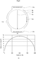
- FIG. 6 shows a circular display panel (in the upper drawing) manufactured by the method of a test example and the result (in the lower drawing) of measurement of parasitic capacitance between the data lines.
- the data lines located within the display area AA are of different lengths.
- the ith data line DLi located at the center of the display area AA has the longest wiring length among the data lines
- the nth data line DLn located on the right edge of the display area AA has the shortest wiring length among the data lines.
- the ith data line DLi was charged with a voltage of approximately 0.03 V and the nth data line DLn was charged with a voltage of approximately 0.4 V.
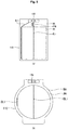
- FIG. 7 shows a circular display panel (in the upper drawing) manufactured by the method of an exemplary embodiment and the result (in the lower drawing) of measurement of parasitic capacitance between the data lines.
- the data lines located within the display area AA are of different lengths.
- a compensating capacitor Ck or Cn (or dummy capacitor) is added to a data line.
- One side of the compensating capacitor Ck or Cn may be connected to a data line, and the other side may be electrically floating or connected to a power source (a power source or static source that delivers a particular voltage), as illustrated in the figure.
- the other side of the compensating capacitor Ck or Cn is electrically floating, there is a possibility that its characteristics may vary due to neighboring signal lines, internal or external environment factors, etc. In contrast, if the other side of the compensating capacitor Ck or Cn is connected to a power source, the capacitance of the capacitor remains constant and therefore the possibility of characteristic variation can be avoided.
- the ith data line DLi located at the center of the display area AA has the longest wiring length among the data lines
- the nth data line DLn located on the right edge of the display area AA has the shortest wiring length among the data lines.
- a compensating capacitor exists on the ith data line DLi.
- a compensating capacitor exists on the nth data line DLn.
- compensating capacitors exist on the data lines between the ith data line DLi and the nth data line DLn.
- a compensating capacitor Ck exists on the kth data line DLk between the ith data line DLi and the nth data line DLn.
- the compensating capacitors have an appropriate capacitance value depending on the length of each data line. Particularly, the compensating capacitors are set to have a capacitance value that can compensate for variations in parasitic capacitance - the capacitance of parasitic capacitors - between the data lines through a preliminary test.
- the ith data line DLi, kth data line DLk, and nth data line DLn were charged with almost the same/similar voltage so as to overcome the problem of luminance non-uniformity although there are some differences in voltage.
- the data line wiring area may be largely divided into three sections, and compensating capacitors may be provided in one or more of these sections.
- compensating capacitors may be provided in the upper and lower portions of the display area.
- the data line wiring area comprises a data routing part, an active area part, and a dummy capacitor part.
- the data routing part corresponds to an upper non-display area (or link area) existing between the data driver 130 and the display area AA.
- the active area part corresponds to a wiring area existing in the display area AA.
- the dummy capacitor part corresponds to a lower non-display area existing between the display area AA and the non-display area NA.
- Compensating capacitors C1, C2, C5, and C6 are provided at the data routing part and dummy capacitor part existing in the upper and lower portions of the display area AA.
- a design scheme for compensating for variations relative to a shorter data line DL and the longest data line DL among the data lines will be described below.
- the test result showed that the parasitic capacitors between the data lines may be designed with variation ranging from 1 to 20 % by forming the compensating capacitors C1, C2, C5, and C6 on the display panel using the scheme in the exemplary embodiment.
- the parasitic capacitors existing on the data lines may be set to have a capacitance value, with variation ranging from 1 to 20 %, and the maximum extent of variation is narrowed down to 15 %, 10 %, 5 %, etc. by optimization.
- the parasitic capacitors between the data lines had variation ranging from 1 to 20 %, the problem that the left and right sides of the display area look brighter due to luminance non-uniformity could be solved. More preferably, the parasitic capacitors between the data lines may be optimized to have a variation of 1 to 10 % or less.
- the compensating capacitors may be placed using one of the following examples.
- FIG. 9 illustrates a first example of placement of compensating capacitors.
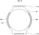
- FIG. 10 illustrates a second example of placement of compensating capacitors.
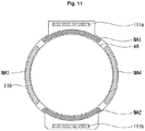
- FIG. 11 illustrates a third example of placement of compensating capacitors.
- FIG. 12 is a view showing a non-display area where compensating capacitors are arranged.
- the compensating capacitors are arranged in non-display areas NA1 and NA2 provided on the upper and lower sides of the display area AA of the display panel 110.
- the first and second compensating capacitors C1 and C2 may be arranged in the upper non-display area NA1
- the fifth and sixth compensating capacitors C5 and C6 may be arranged in the lower non-display area NA2.
- the compensating capacitors are arranged in non-display areas NA3 and NA4 provided on the left and right sides of the display area AA of the display panel 110.
- the first and fifth compensating capacitors C1 and C5 may be arranged in the left non-display area NA3
- the second and sixth compensating capacitors C2 and C6 may be arranged in the right non-display area NA4.
- the compensating capacitors are arranged in non-display areas NA1, NA2, NA3, and NA4 provided on the upper, lower, left, and right sides of the display area AA of the display panel 110.
- the first, second, fifth, and sixth compensating capacitors C1, C2, C5, and C6 may be respectively arranged in the non-display areas NA1, NA2, NA3, and NA4 provided in the upper, lower, left, and right sides.
- the first and fifth compensating capacitors C1 and C5 or second and sixth compensating capacitors C2 and C6 in this area have a difference in level as if each data line forms a step-like profile.
- the compensating capacitors may have a different capacitance value depending on the length of the data lines, as shown in FIG. 7 , and may converge to a single capacitance value in some parts. For example, if the data lines are separated from one another, with differences in level, as shown in FIG. 12 , N adjacent data lines (N is an integer is an integer greater than or equal to 2) may be combined into one group, and the compensating capacitor corresponding to this group may converge to a single capacitance value.
- the compensating capacitors C1, C2, C5, and C6 may be provided based on a metal layer (first electrode layer of the compensating capacitors) and an active layer (second electrode layer of the compensating capacitors) metallized by doping, etc., with an insulating film (e.g., inorganic or organic film) interposed between them.
- the compensating capacitors C1, C2, C5, and C6 may be provided based on M metal layers (M is an integer greater than or equal to 2) and an active layer metalized by doping, etc.
- the metallized active layer is an active layer that constitutes transistors, etc. for a subpixel, and refers to a layer based on oxide semiconductor (e.g., IGZO).
- oxide semiconductor e.g., IGZO
- the oxide semiconductor has metal properties, rather than semiconductor properties, by a process such as doping.
- the circular display panels of the above-described test example and exemplary embodiment are based on the following subpixel circuit.
- FIG. 13 is a view of the circuit configuration of a subpixel used in the circular display panels of the test example and exemplary embodiment.
- FIG. 14 is a driving waveform diagram of the circular display panel of FIG. 13 .
- a subpixel has a 7T (transistor) 1C (capacitor) structure.
- a second transistor T2a and T2b has a dual-transistor structure by way of example, and also may have a single-transistor structure.
- the transistors included in a subpixel are P-type transistors, but they also may be N-type transistors.
- the positions of source and drain electrodes may vary depending on the type of the transistors, and the source and drain electrodes may be referred to as first and second electrodes in the following description.
- a first transistor T1 has a gate electrode connected to a 1 a-th gate line GL1a, a first electrode connected to a first data line DL1, and a second electrode connected to one end of a storage capacitor Cstg.
- the first transistor T1 serves to deliver a data signal, supplied through the first data line DL1, to the storage capacitor Cstg, in response to a 1 a-th gate signal SCAN1.
- the 2a-th transistor T2a has a gate electrode connected to a 1b-th gate line GL1b, a first electrode connected to a gate electrode of a driving transistor DT, and a second electrode connected to a first electrode of the 2b-th transistor T2b.
- the 2b-th transistor T2b has a gate electrode connected to the 1 b-th gate line GL1 b, a first electrode connected to the second electrode of the 2a-th transistor T2a, and a second electrode connected to a second electrode of the driving transistor DT.
- the 2a-th transistor T2a and 2b-th transistor T2b serve to make a diode connection between the gate and source electrodes of the driving transistor DT, in response to a 1 b-th gate signal SCAN2.
- a third transistor T3 has a gate electrode connected to a 1c-th gate line GL1c, a first electrode connected to a reference voltage line VREF, and a second electrode connected to one end of the storage capacitor Cstg.
- the third transistor T3 serves to supply a reference voltage Vref (or compensation voltage) to one end of the storage capacitor Cstg in response to a 1c-th gate signal EM.
- a fourth transistor T4 has a gate electrode connected to a 1c-th gate line GL1c, a first electrode connected to the second electrode of the driving transistor DT, and a second electrode connected to the anode of an organic light-emitting diode OLED.
- the fourth transistor T4 serves to deliver drive current to the organic light-emitting diode OLED and causes it to emit light in response to the 1 c-th gate signal EM.
- a fifth transistor T5 has a gate electrode connected to the 1 b-th gate line GL1 b, a first electrode connected to the reference voltage line VREF, and a second electrode connected to the anode of the organic light-emitting diode OLED.
- the fifth transistor T5 serves to supply the reference voltage Vref to the anode of the organic light-emitting diode OLED in response to the 1b-th gate signal SCAN2.
- the driving transistor DT has a gate electrode connected to the other end of the storage capacitor Cstg, a first electrode connected to a first power supply line EVDD, and a second electrode connected to the first electrode of the fourth transistor T4.
- the driving transistor DT turns on in response to a data voltage supplied from the storage capacitor Cstg, and generates a drive current to supply it to the organic light-emitting diode OLED.
- the organic light-emitting diode OLED has the anode connected to the second electrode of the fourth transistor T4 and the cathode connected to a second power supply line EVDD.
- the organic light-emitting diode OLED serves to emit light in response to the drive current delivered through the fourth transistor T4.
- the subpixel configured as above has a compensation period during which compensation operation for compensating the threshold voltage Vth of the driving transistor DT is performed. During the compensation period, the compensation operation is performed, including supplying the reference voltage Vref to the reference voltage line VREF and diode-connecting the driving transistor DT.
- the 1a-th gate signal SCAN1 and the 1 b-th gate signal SCAN2 are in the logic-low state, and the 1 c-th gate signal EM is in the logic-high state. Accordingly, the driving transistor DT is diode-connected, and the first data line DL1 is electrically floating.
- the concept of this disclosure may apply to signal lines - that is, lines that provide signals or voltage - which are located in the display area, and whose wiring length differs with respect to a first area.
- the first area may be defined as the area where the signal line with the longest wiring length, like the ith data line of FIG. 7 , among all the signal lines, is placed.
- the first area may be an area other than the center.
- the present disclosure can solve the problem of luminance non-uniformity and improve display quality by preventing or reducing variations in parasitic elements (e.g., parasitic capacitance) that inevitably exist between signal lines of an odd-shaped display panel. Moreover, the present disclosure can prevent or reduce variations in compensating voltage due to differences in the wiring length of signal lines arranged within a display area. In addition, the present disclosure can make the luminance of the display panel uniform by compensating for variations in the capacitance of parasitic capacitors.
- parasitic elements e.g., parasitic capacitance
Landscapes
- Engineering & Computer Science (AREA)
- Physics & Mathematics (AREA)
- General Physics & Mathematics (AREA)
- Microelectronics & Electronic Packaging (AREA)
- Nonlinear Science (AREA)
- Computer Hardware Design (AREA)
- Theoretical Computer Science (AREA)
- Crystallography & Structural Chemistry (AREA)
- Chemical & Material Sciences (AREA)
- Optics & Photonics (AREA)
- Mathematical Physics (AREA)
- Manufacturing & Machinery (AREA)
- Geometry (AREA)
- Control Of Indicators Other Than Cathode Ray Tubes (AREA)
- Electroluminescent Light Sources (AREA)
- Devices For Indicating Variable Information By Combining Individual Elements (AREA)
- Diaphragms For Electromechanical Transducers (AREA)
Abstract
Description
- This application claims the priority benefit of Korean Patent Application No.
10-2015-0166483 filed on November 26, 2015 - The present disclosure relates to a display device and a method for manufacturing the same.
- With the development of information technology, the market for displays that play an intermediary role between users and information is growing. Thus, display devices such as organic light-emitting displays (OLEDs), quantum dot displays (QDDs), liquid crystal displays (LCDs), and plasma display panels (PDPs) are increasingly used.
- The above-explained display devices each comprise a display panel comprising a plurality of subpixels, a drive part that outputs a drive signal to drive the display panel, a power supply that generates and supplies power to the drive part.
- A display device comes in a small, medium, or large size. The configuration of the display panel, drive devices (including peripherals) connected to the display panel, and a structure for housing the display panel and the drive devices may vary depending on the desired size, shape, application, etc. of the display device.
- The use and usage environment of display devices is getting more diversified. To cope with this, display panels for displaying images are diversifying from a traditional square or rectangular shape to a circular shape as well as a curved shape.
- An odd-shaped display device composed of a display panel with a circular shape, elliptical shape, etc. offers some advantages such as greater freedom of design. However, the conventional odd-shaped display devices proposed have the problem of non-uniform luminance due to variations in parasitic elements (e.g., parasitic capacitance) that inevitably exist between signal lines of the display panel - that is, differences in luminance between the signal lines. Thus, there is a need for a solution to this problem.
- The present disclosure provides a display device comprising a display area, a non-display area, signal lines, and compensating capacitors. The display area and the non-display area are defined on a substrate. The signal lines are located within the display area, and their wiring length differs depending on location. The compensating capacitors are connected to at least one of the signal lines.
- In one or more embodiments, the compensating capacitors have a different capacitance value depending on the length of the signal lines.
- In one or more embodiments, adjacent N signal lines (N is an integer greater than or equal to 2) are combined into one group, and the compensating capacitor corresponding to the group converges to a single capacitance value.
- In one or more embodiments, the compensating capacitors are formed so that parasitic capacitors existing between the signal lines have a capacitance value, with variation ranging from 1 to 20 %.
- In one or more embodiments, the compensating capacitors are arranged in non-display areas provided on the upper and lower sides of the display area.
- In one or more embodiments, the compensating capacitors are arranged in non-display areas provided on the left and right sides of the display area.
- In one or more embodiments, the compensating capacitors are arranged in non-display areas provided on the upper, lower, left, and right sides of the display area.
- In one or more embodiments, one end of the compensating capacitors is connected to at least one of the signal lines, and the other end is electrically floating or connected to a power source.
- In another aspect, the present disclosure provides a method for manufacturing a display device. The method for manufacturing a display device comprises: defining a display area and a non-display area on a substrate; arranging signal lines whose wiring length differs depending on location, within the display area; and forming compensating capacitors in such a manner that each compensating capacitor is connected to at least one of the signal lines.
- In one or more embodiments, in the forming of the compensating capacitors, the compensating capacitors have a different capacitance value depending on the length of the signal lines.
- The accompanying drawings, which are included to provide a further understanding of the invention and are incorporated in and constitute a part of this specification, illustrate embodiments of the invention and together with the description serve to explain the principles of the invention. In the drawings:
-
FIG. 1 is a block diagram schematically showing a display device according to an exemplary embodiment of the present disclosure; -
FIG. 2 is a view schematically showing the configuration of a subpixel ofFIG. 1 ; -
FIG. 3 is a block diagram schematically showing a display device for a smartwatch according to an exemplary embodiment of the present disclosure; -
FIG. 4 is a top plan view schematically showing a display panel for the smartwatch ofFIG. 3 ; -
FIG. 5 is a view for explaining the cause of luminance non-uniformity in a rectangular display panel and a circular display panel; -
FIG. 6 is a view for explaining a problem with a test example; -
FIG. 7 is a view for explaining the concept of compensation according to an exemplary embodiment of the present disclosure; -
FIG. 8 is a view for explaining a design scheme for a compensating capacitor according to an exemplary embodiment of the present disclosure; -
FIG. 9 illustrates a first example of placement of compensating capacitors; -
FIG. 10 illustrates a second example of placement of compensating capacitors; -
FIG. 11 illustrates a third example of placement of compensating capacitors; -
FIG. 12 is a view showing a non-display area where compensating capacitors are arranged; -
FIG. 13 is a view of the circuit configuration of a subpixel used in the circular display panels of the test example and exemplary embodiment; and -
FIG. 14 is a driving waveform diagram of the circular display panel ofFIG. 13 . - Reference will now be made in detail to embodiments illustrated in the accompanying drawings, examples of which are illustrated in the accompanying drawings.
- A concrete embodiment of the present invention will be described below with reference to the accompanying drawings.
-
FIG. 1 is a block diagram schematically showing a display device according to an exemplary embodiment of the present disclosure.FIG. 2 is a view schematically showing the configuration of a subpixel ofFIG. 1 . - As illustrated in
FIG. 1 , the display device basically comprises ahost system 1000, atiming controller 170, adata driver 130, apower supply 140, agate driver 150, and adisplay panel 110. - The
host system 1000 comprises a system-on-chip (SoC) with a scaler embedded in it, and converts digital video data of an input image into a data signal in a format suitable for display on thedisplay panel 110. Thehost system 1000 transmits various timing signals, together with the data signal, to thetiming controller 170. - The
timing controller 170 controls the operation timings of thedata driver 130 andgate driver 150 based on timing signals, such as a vertical synchronization signal, horizontal synchronization signal, data enable signal, and main clock, received from thehost system 1000. Thetiming controller 170 performs image processing (such as data compensation, etc.) of the data signal received from thehost system 1000 and supplies it to thedata driver 130. - The
data driver 130 operates in response to a first drive signal DDC, etc. output from thetiming controller 170. Thedata driver 130 converts a digital data signal DATA received from thetiming controller 170 to an analog data signal and outputs it. - The
data driver 130 converts a digital data signal DATA to an analog data signal in response to a gamma voltage of a gamma part (not shown) provided internally or externally. Thedata driver 130 supplies a data signal to data lines DL1 to DLn of thedisplay panel 110. - The
gate driver 150 operates in response to a second drive signal GDC, etc. output from thetiming controller 170. Thegate driver 150 outputs a gate signal (or scan signal) at a gate-high voltage or gate-low voltage in response to the second drive signal GDC, etc. - The
gate driver 150 may sequentially output a gate signal in a forward or backward direction. Thegate driver 150 supplies a gate signal to gate lines GL1 to GLm of thedisplay panel 110. - The
power supply 140 produces first and second power-supply voltages EVDD and EVSS for driving thedisplay panel 110 and third and fourth power-supply voltages VCC and GND for driving thedata driver 130. Besides, thepower supply 140 generates voltages needed to drive the display device, such as the gate-high voltage, gate-low voltage, etc., that are delivered to thegate driver 150. - The
display panel 110 comprises subpixels SP, the data lines DL1 to DLn connected to the subpixels SP, and the gate lines GL1 to GLm connected to the subpixels SP. Thedisplay panel 110 displays an image in response to a gate signal output from thegate driver 150 and a data signal DATA output from thedata driver 130. Thedisplay panel 110 comprises a lower substrate and an upper substrate. The subpixels SP are formed between the lower substrate and the upper substrate. - As illustrated in
FIG. 2 , one subpixel comprises a transistor T1 connected to the gate line GL1 and data line DL1 (or formed at the intersection between the gate line GL1 and data line DL1), and a pixel circuit PC that operates in response to a data signal DATA supplied through the transistor T1. - The
display panel 110 is implemented as a liquid crystal display panel or an organic light-emitting display panel depending on the configuration of the pixel circuits PC of the subpixels SP. If thedisplay panel 110 is implemented as a liquid crystal display panel, it operates in TN (Twisted Nematic) mode, VA (Vertical Alignment) mode, IPS (In-Plane Switching) mode, FFS (Fringe Field Switching) mode, or ECB (Electrically Controlled Birefringence) mode. - If the
display panel 110 is implemented as an organic light-emitting display panel, it operates as a top-emission type, bottom-emission type, or dual-emission type. - The above-explained display device may be implemented for a television system, a set-top box, a navigation system, a video player, a Blu-ray player, a personal computer (PC), a wearable device, a home theater system, a mobile phone, etc.
- The display panel of the display device may be a liquid crystal display panel, an organic light-emitting display panel, an electrophoretic display panel, a quantum dot display panel, a plasma display panel, etc. For convenience of explanation, a display device having an organic light-emitting display panel will be described below by way of an example of the display panel.
- The display device to be described below may come in a small, medium, or large size. By way of example, a small display, which can bring significant power consumption savings compared to medium or large displays, will be described below.
- By way of example, a smartwatch, which is a type of small display, according to an exemplary embodiment of the present disclosure will be described. Moreover, the following description will be given of an example in which one pixel consists of red, green, and blue subpixels RGB. However, it should be noted that this is just an illustration and the present disclosure is not limited thereto.
-
FIG. 3 is a block diagram schematically showing a display device for a smartwatch according to an exemplary embodiment of the present disclosure. -
FIG. 4 is a top plan view schematically showing a display panel for the smartwatch ofFIG. 3 . - As illustrated in
FIG. 3 , asmartwatch 100 comprises a host system (HS) 1000, a timing controller (TCON) 170, a data driver (DIC) 130, a power supply (PIC) 140, agate driver 150, a display panel (PNL) 110, and a touch driver (TIC) 190. - The
smartwatch 100 corresponds to a small display. In the small display device, some part of the device is integrated to reduce the device's complexity. For example, thepower supply 140 may be included within thedata driver 130. However, this is just an illustration, and the small display may be implemented in a variety of configurations, including integrating thetiming controller 170 and thedata driver 130 into a single unit. - The
gate driver 150 is embedded in thedisplay panel 110, together with a pixel array. Thegate driver 150 embedded in thedisplay panel 110 is formed by the GIP (gate-in-panel) technology, along with a thin-film transistor process. - The
smartwatch 100 has thetouch driver 190 as touch-type input means to help the user input data. Moreover, thedisplay panel 110 comprises touch sensors that sense a touch position using thetouch driver 190 and output the value of the sensed position, and sensor lines that electrically connect the touch sensors and thetouch driver 190. - The
touch driver 190 detects information on the position of a finger touch using self-capacitive touch sensors or mutual capacitive touch sensors. Thetouch driver 190 transmits the detected information on the position of the finger touch to thehost system 1000. Thehost system 1000 executes an application associated with the touch position information received from thetouch driver 190. - As illustrated in
FIG. 4 , thedisplay panel 110 may be formed in a circular shape, for example. As well as the circular shape, thedisplay panel 110 may be formed in various shapes including a square shape, rectangular shape, polygonal shape, elliptical shape, etc. - Red, green, and blue subpixels R, G, and B and touch sensors (not shown) are placed in a display area AA of the
display panel 110. Apad part 111 a may be placed in a pad area PA defined in a non-display area (or bezel region) NA of thedisplay panel 110. By way of example, thepad part 111 a is placed only on top of the display area AA, but also may be placed under the display area AA. - The
data driver 130 with the power supply is mounted on a flexible circuit substrate (film) 180. Theflexible circuit substrate 180 is electrically connected to thepad part 111 a through an anisotropic conductive film (ACF), etc. Other devices needed to drive thedisplay panel 110, as well as thedata driver 130, may be mounted on theflexible circuit substrate 180. - As stated above, with the diversification of the use and usage environment of display devices, display panels for displaying images are diversifying from a traditional square or rectangular shape to a circular shape as well as a curved shape.
- An odd-shaped display device composed of a display panel with a circular shape, elliptical shape, etc., rather than a square or rectangular shape, offers some advantages such as greater freedom of design. However, the conventional odd-shaped display devices proposed have the problem of luminance non-uniformity due to variations in parasitic elements (e.g., parasitic capacitance) that inevitably exist between signal lines of the display panel - that is, differences in luminance between the signal lines. Thus, there is a need for a solution to this problem.
- Now, the cause of luminance non-uniformity due to parasitic elements and how the present disclosure will solve this problem will be described on the basis of a rectangular display panel and a circular display panel.
-
FIG. 5 is a view for explaining the cause of luminance non-uniformity in a rectangular display panel and a circular display panel.FIG. 6 is a view for explaining a problem with a test example.FIG. 7 is a view for explaining the concept of compensation according to an exemplary embodiment of the present disclosure.FIG. 8 is a view for explaining a design scheme for a compensating capacitor according to an exemplary embodiment of the present disclosure. - In a
rectangular display panel 110 shown in (a) ofFIG. 5 , the data lines located within the display area AA are arranged in such a way that they are equal in length. As an example, the first data line DL1 located in the first row on the left side within the display area AA and the ith data line DLi located in the ith row at the center within the display area AA are equal in length. This is because the data line wiring paths remain the same within the display area AA. - By contrast, the data lines located within a link area existing between the
data driver 130 and the display area AA are arranged in such a way that at least one of them has a different length. As an example, the first data line DL1 is arranged diagonally within the link area between thedata driver 130 and the display area AA, whereas the ith data line DLi located between thedata driver 130 and the display area AA is arranged in a straight line and therefore a offset compensation pattern PTN may be added to the link area. - This is because the data line wiring paths change with every Mth line (M is an integer greater than or equal to 1) within the link area. This means that the length of the data lines and the number of pixels connected to the data lines change with every M lines.
- In a
circular display panel 110 shown in (b) ofFIG. 5 , the data lines located within the display area AA are arranged in such a way that they are all of different lengths. Also, the data lines located within the link area existing between thedata driver 130 and the display area AA are arranged in such a way that at least one of them has a different length. - Structurally speaking, the rectangular display panel may have more extra space like the non-display area NA, as compared to the circular display panel. Accordingly, to overcome the problem of luminance non-uniformity due to variations in parasitic elements (e.g., parasitic capacitance) between signal lines - that is, differences in luminance between the signal lines, a offset compensation pattern PTN may be easily added to the link area between the
data driver 130 and the display area AA. With the offset compensation pattern PTN, resistance is kept the same by adjusting the length of the data lines to match the time constant (t = R X C) of a data signal. - By contrast, structurally speaking, the circular display panel can hardly have more extra space like the non-display area NA, as compared to the rectangular display panel. Moreover, the test result showed that adding the offset compensation pattern PTN to the link area to keep resistance the same between the data lines was not enough to solve the problem of luminance non-uniformity.
-
FIG. 6 shows a circular display panel (in the upper drawing) manufactured by the method of a test example and the result (in the lower drawing) of measurement of parasitic capacitance between the data lines. In the circular display panel in the test example, the data lines located within the display area AA are of different lengths. - As illustrated in the figure, the ith data line DLi located at the center of the display area AA has the longest wiring length among the data lines, whereas the nth data line DLn located on the right edge of the display area AA has the shortest wiring length among the data lines.
- The result of applying a test voltage to the circular display panel of the test example and measuring the capacitor values of the ith data line DLi and nth data line DLn showed that an offset of approximately 13 to 15 pF existed between the ith data line DLi and the nth data line DLn.
- Also, it was observed that, after supplying a data voltage to the circular display panel of the test example, the ith data line DLi was charged with a voltage of approximately 0.03 V and the nth data line DLn was charged with a voltage of approximately 0.4 V.
- As a consequence, when an image was displayed on the circular display panel of the test example, every variation in the voltage stored in the data lines was fully reflected, as shown in the lower drawing of
FIG. 6 . Accordingly, it was observed that the circular display panel had differences in luminance, which made the left and right areas to look brighter than the center. - In a number of tests conducted to find a solution to the problem of luminance non-uniformity, which may occur only in odd-shaped display panels like a circular display panel, based on the test example, the following exemplary embodiment exhibits excellent results, so the concept of this exemplary embodiment will be described.
-
FIG. 7 shows a circular display panel (in the upper drawing) manufactured by the method of an exemplary embodiment and the result (in the lower drawing) of measurement of parasitic capacitance between the data lines. In the circular display panel in the exemplary embodiment, the data lines located within the display area AA are of different lengths. - A compensating capacitor Ck or Cn (or dummy capacitor) is added to a data line. One side of the compensating capacitor Ck or Cn may be connected to a data line, and the other side may be electrically floating or connected to a power source (a power source or static source that delivers a particular voltage), as illustrated in the figure.
- If the other side of the compensating capacitor Ck or Cn is electrically floating, there is a possibility that its characteristics may vary due to neighboring signal lines, internal or external environment factors, etc. In contrast, if the other side of the compensating capacitor Ck or Cn is connected to a power source, the capacitance of the capacitor remains constant and therefore the possibility of characteristic variation can be avoided.
- As illustrated in the figure, the ith data line DLi located at the center of the display area AA has the longest wiring length among the data lines, whereas the nth data line DLn located on the right edge of the display area AA has the shortest wiring length among the data lines.
- No compensating capacitor exists on the ith data line DLi. By contrast, a compensating capacitor exists on the nth data line DLn. Also, compensating capacitors exist on the data lines between the ith data line DLi and the nth data line DLn. For example, a compensating capacitor Ck exists on the kth data line DLk between the ith data line DLi and the nth data line DLn.
- The compensating capacitors have an appropriate capacitance value depending on the length of each data line. Particularly, the compensating capacitors are set to have a capacitance value that can compensate for variations in parasitic capacitance - the capacitance of parasitic capacitors - between the data lines through a preliminary test.
- The result of applying a test voltage to the circular display panel of the exemplary embodiment and measuring the capacitor values of the ith data line DLi, kth data line DLk, and nth data line DLn showed that an offset of approximately 1 to 4 pF existed among the ith data line DLi, kth data line DLk, and nth data line DLn.
- Also, it was observed that, after supplying a data voltage to the circular display panel of the exemplary embodiment, the ith data line DLi, kth data line DLk, and nth data line DLn were charged with almost the same/similar voltage so as to overcome the problem of luminance non-uniformity although there are some differences in voltage.
- As a consequence, when an image was displayed on the circular display panel of the exemplary embodiment, the variation in the voltage stored in the data lines was cancelled out, as in the lower drawing of
FIG. 7 . Accordingly, it was observed that the differences in luminance on the circular display panel, which made the left and right areas to look brighter than the center, were substantially reduced (or mitigated). - In the present disclosure, the data line wiring area may be largely divided into three sections, and compensating capacitors may be provided in one or more of these sections. For convenience of explanation, the following description will be given with an example where compensating capacitors are provided in the upper and lower portions of the display area.
- As illustrated in
FIG. 8 , the data line wiring area comprises a data routing part, an active area part, and a dummy capacitor part. - The data routing part corresponds to an upper non-display area (or link area) existing between the
data driver 130 and the display area AA. The active area part corresponds to a wiring area existing in the display area AA. The dummy capacitor part corresponds to a lower non-display area existing between the display area AA and the non-display area NA. - Compensating capacitors C1, C2, C5, and C6 are provided at the data routing part and dummy capacitor part existing in the upper and lower portions of the display area AA. A design scheme for compensating for variations relative to a shorter data line DL and the longest data line DL among the data lines will be described below.
- R1 = R2: Resistance is kept the same by adjusting the length of the data lines
- R3 = n1 × R_unit (n1 (<n2): the number of pixels on the shorter data line)
- R4 = n2 × R_unit (n2: the number of pixels on the longest data line)
- R5, R6: Compensation resistors (or dummy resistors) on the data lines
- C3 = n1 × C_unit
- C4 = n2 × C_unit
- C1, C2, C5, C6: Compensating capacitors on the data lines in the upper and lower portions of the display area
- (R_unit, C_unit: resistors and parasitic capacitors for an array of pixels)

- The test result showed that the parasitic capacitors between the data lines may be designed with variation ranging from 1 to 20 % by forming the compensating capacitors C1, C2, C5, and C6 on the display panel using the scheme in the exemplary embodiment.
- As above, the parasitic capacitors existing on the data lines may be set to have a capacitance value, with variation ranging from 1 to 20 %, and the maximum extent of variation is narrowed down to 15 %, 10 %, 5 %, etc. by optimization.
- It was observed that, if the parasitic capacitors between the data lines had variation ranging from 1 to 20 %, the problem that the left and right sides of the display area look brighter due to luminance non-uniformity could be solved. More preferably, the parasitic capacitors between the data lines may be optimized to have a variation of 1 to 10 % or less.
- By designing the compensating capacitors C1, C2, C5, and C6 on the display panel using the scheme in the exemplary embodiment and optimizing them, the problem of luminance non-uniformity can be solved.
- The compensating capacitors may be placed using one of the following examples.
-
FIG. 9 illustrates a first example of placement of compensating capacitors.FIG. 10 illustrates a second example of placement of compensating capacitors.FIG. 11 illustrates a third example of placement of compensating capacitors.FIG. 12 is a view showing a non-display area where compensating capacitors are arranged. - As illustrated in
FIG. 9 , the compensating capacitors are arranged in non-display areas NA1 and NA2 provided on the upper and lower sides of the display area AA of thedisplay panel 110. For example, the first and second compensating capacitors C1 and C2 may be arranged in the upper non-display area NA1, and the fifth and sixth compensating capacitors C5 and C6 may be arranged in the lower non-display area NA2. - As illustrated in
FIG. 10 , the compensating capacitors are arranged in non-display areas NA3 and NA4 provided on the left and right sides of the display area AA of thedisplay panel 110. For example, the first and fifth compensating capacitors C1 and C5 may be arranged in the left non-display area NA3, and the second and sixth compensating capacitors C2 and C6 may be arranged in the right non-display area NA4. - As illustrated in
FIG. 11 , the compensating capacitors are arranged in non-display areas NA1, NA2, NA3, and NA4 provided on the upper, lower, left, and right sides of the display area AA of thedisplay panel 110. For example, the first, second, fifth, and sixth compensating capacitors C1, C2, C5, and C6 may be respectively arranged in the non-display areas NA1, NA2, NA3, and NA4 provided in the upper, lower, left, and right sides. - As illustrated in
FIG. 12 , when the area existing between the display area AA and the non-display area NA is viewed on a magnified scale, it is not curved but stepped. Therefore, the first and fifth compensating capacitors C1 and C5 or second and sixth compensating capacitors C2 and C6 in this area have a difference in level as if each data line forms a step-like profile. - The compensating capacitors may have a different capacitance value depending on the length of the data lines, as shown in
FIG. 7 , and may converge to a single capacitance value in some parts. For example, if the data lines are separated from one another, with differences in level, as shown inFIG. 12 , N adjacent data lines (N is an integer is an integer greater than or equal to 2) may be combined into one group, and the compensating capacitor corresponding to this group may converge to a single capacitance value. - Meanwhile, the compensating capacitors C1, C2, C5, and C6 may be provided based on a metal layer (first electrode layer of the compensating capacitors) and an active layer (second electrode layer of the compensating capacitors) metallized by doping, etc., with an insulating film (e.g., inorganic or organic film) interposed between them. Also, the compensating capacitors C1, C2, C5, and C6 may be provided based on M metal layers (M is an integer greater than or equal to 2) and an active layer metalized by doping, etc.
- In the above description, the metallized active layer is an active layer that constitutes transistors, etc. for a subpixel, and refers to a layer based on oxide semiconductor (e.g., IGZO). The oxide semiconductor has metal properties, rather than semiconductor properties, by a process such as doping.
- The circular display panels of the above-described test example and exemplary embodiment are based on the following subpixel circuit.
-
FIG. 13 is a view of the circuit configuration of a subpixel used in the circular display panels of the test example and exemplary embodiment.FIG. 14 is a driving waveform diagram of the circular display panel ofFIG. 13 . - As illustrated in
FIGS. 13 and14 , a subpixel has a 7T (transistor) 1C (capacitor) structure. A second transistor T2a and T2b has a dual-transistor structure by way of example, and also may have a single-transistor structure. - The following description will be given with an example where the transistors included in a subpixel are P-type transistors, but they also may be N-type transistors. As such, the positions of source and drain electrodes may vary depending on the type of the transistors, and the source and drain electrodes may be referred to as first and second electrodes in the following description.
- A first transistor T1 has a gate electrode connected to a 1 a-th gate line GL1a, a first electrode connected to a first data line DL1, and a second electrode connected to one end of a storage capacitor Cstg. The first transistor T1 serves to deliver a data signal, supplied through the first data line DL1, to the storage capacitor Cstg, in response to a 1 a-th gate signal SCAN1.
- The 2a-th transistor T2a has a gate electrode connected to a 1b-th gate line GL1b, a first electrode connected to a gate electrode of a driving transistor DT, and a second electrode connected to a first electrode of the 2b-th transistor T2b. The 2b-th transistor T2b has a gate electrode connected to the 1 b-th gate line GL1 b, a first electrode connected to the second electrode of the 2a-th transistor T2a, and a second electrode connected to a second electrode of the driving transistor DT. The 2a-th transistor T2a and 2b-th transistor T2b serve to make a diode connection between the gate and source electrodes of the driving transistor DT, in response to a 1 b-th gate signal SCAN2.
- A third transistor T3 has a gate electrode connected to a 1c-th gate line GL1c, a first electrode connected to a reference voltage line VREF, and a second electrode connected to one end of the storage capacitor Cstg. The third transistor T3 serves to supply a reference voltage Vref (or compensation voltage) to one end of the storage capacitor Cstg in response to a 1c-th gate signal EM.
- A fourth transistor T4 has a gate electrode connected to a 1c-th gate line GL1c, a first electrode connected to the second electrode of the driving transistor DT, and a second electrode connected to the anode of an organic light-emitting diode OLED. The fourth transistor T4 serves to deliver drive current to the organic light-emitting diode OLED and causes it to emit light in response to the 1 c-th gate signal EM.
- A fifth transistor T5 has a gate electrode connected to the 1 b-th gate line GL1 b, a first electrode connected to the reference voltage line VREF, and a second electrode connected to the anode of the organic light-emitting diode OLED. The fifth transistor T5 serves to supply the reference voltage Vref to the anode of the organic light-emitting diode OLED in response to the 1b-th gate signal SCAN2.
- The driving transistor DT has a gate electrode connected to the other end of the storage capacitor Cstg, a first electrode connected to a first power supply line EVDD, and a second electrode connected to the first electrode of the fourth transistor T4. The driving transistor DT turns on in response to a data voltage supplied from the storage capacitor Cstg, and generates a drive current to supply it to the organic light-emitting diode OLED.
- The organic light-emitting diode OLED has the anode connected to the second electrode of the fourth transistor T4 and the cathode connected to a second power supply line EVDD. The organic light-emitting diode OLED serves to emit light in response to the drive current delivered through the fourth transistor T4.
- The subpixel configured as above has a compensation period during which compensation operation for compensating the threshold voltage Vth of the driving transistor DT is performed. During the compensation period, the compensation operation is performed, including supplying the reference voltage Vref to the reference voltage line VREF and diode-connecting the driving transistor DT.
- During the compensation period, the 1a-th gate signal SCAN1 and the 1 b-th gate signal SCAN2 are in the logic-low state, and the 1 c-th gate signal EM is in the logic-high state. Accordingly, the driving transistor DT is diode-connected, and the first data line DL1 is electrically floating.
- Parasitic capacitors exist on the first data line DL1 as explained previously. Thus, the gate node voltage of the driving transistor DT rises when sampled to compensate (EVDD-Vth -> EVDD - |Vth|) the threshold voltage Vth of the driving transistor DT.
- As in the lower portion of the image of
FIG. 13 showing a change in the gate node voltage of the driving transistor DT, voltage is distributed in the direction of "Cstg" and the direction of "Cdata". - In terms of design, while the capacitance of the storage capacitor Cstg is kept the same, voltage varies with the length of the data lines, which results in differences in luminance. For reference, the less Cdata, the stronger the coupling effect. In this case, the differences in luminance due to differences in data voltage depend on the degree of the coupling effect.
- Therefore, from the above-described test example in which a circular display panel was manufactured based on subpixels, it was observed that the problem of luminance non-uniformity due to differences in voltage between the data lines (a varies for each data line, as in Reference Voltage Vref + a) since a particular voltage such as the reference voltage is supplied during the compensation period.
- In contrast, from the above-described exemplary embodiment in which a circular display panel was manufactured based on subpixels, it was observed that that the problem of luminance non-uniformity due to voltage variation during the compensation operation was significantly reduced since the variations in parasitic capacitance are reduced by the compensating capacitors provided on the data lines.
- Although the foregoing description has been given of data lines by way of an example of signal lines, the concept of this disclosure may apply to signal lines - that is, lines that provide signals or voltage - which are located in the display area, and whose wiring length differs with respect to a first area. Here, the first area may be defined as the area where the signal line with the longest wiring length, like the ith data line of
FIG. 7 , among all the signal lines, is placed. The first area may be an area other than the center. - As seen from above, the present disclosure can solve the problem of luminance non-uniformity and improve display quality by preventing or reducing variations in parasitic elements (e.g., parasitic capacitance) that inevitably exist between signal lines of an odd-shaped display panel. Moreover, the present disclosure can prevent or reduce variations in compensating voltage due to differences in the wiring length of signal lines arranged within a display area. In addition, the present disclosure can make the luminance of the display panel uniform by compensating for variations in the capacitance of parasitic capacitors.
Claims (10)
- A display device comprising:a display area (AA) and non-display area (NA) defined on a substrate;signal lines whose wiring length differs depending on location, which are located within the display area (AA); andcompensating capacitors (Ck, Cn) each connected to at least one of the signal lines.
- The display device of claim 1, wherein the compensating capacitors (Ck, Cn) have a different capacitance value depending on the length of the signal lines.
- The display device of claim 1 or 2, wherein adjacent N signal lines are combined into one group, and the compensating capacitor corresponding to the group converges to a single capacitance value, wherein N is an integer greater than or equal to 2.
- The display device of any one of claims 1 to 3, wherein the compensating capacitors (Ck, Cn) are formed so that parasitic capacitors existing between the signal lines have a capacitance value, with variation ranging from 1 to 20 %.
- The display device of any one of claims 1 to 4, wherein the compensating capacitors (Ck, Cn) are arranged in non-display areas (NA1, NA2) provided on the upper and lower sides of the display area (AA).
- The display device of any one of claims 1 to 4, wherein the compensating capacitors (Ck, Cn) are arranged in non-display areas (NA3, NA4) provided on the left and right sides of the display area (AA).
- The display device of any one of claims 1 to 4, wherein the compensating capacitors (Ck, Cn) are arranged in non-display areas (NA1, NA2, NA3, NA4) provided on the upper, lower, left, and right sides of the display area (AA).
- The display device of any one of claims 1 to 7, wherein one end of the compensating capacitors (Ck, Cn) is connected to at least one of the signal lines, and the other end is electrically floating or connected to a power source.
- A method for manufacturing a display device, the method comprising:defining a display area (AA) and a non-display area (NA) on a substrate;arranging signal lines whose wiring length differs depending on location, within the display area (AA); andforming compensating capacitors (Ck, Cn) in such a manner that each compensating capacitor (Ck, Cn) is connected to at least one of the signal lines.
- The method of claim 9, wherein, in the forming of the compensating capacitors (Ck, Cn), the compensating capacitors (Ck, Cn) have a different capacitance value depending on the length of the signal lines.
Applications Claiming Priority (1)
| Application Number | Priority Date | Filing Date | Title |
|---|---|---|---|
| KR1020150166483A KR102438782B1 (en) | 2015-11-26 | 2015-11-26 | Display device and manufacturing method thereof |
Publications (1)
| Publication Number | Publication Date |
|---|---|
| EP3174039A1 true EP3174039A1 (en) | 2017-05-31 |
Family
ID=57389305
Family Applications (1)
| Application Number | Title | Priority Date | Filing Date |
|---|---|---|---|
| EP16199973.5A Ceased EP3174039A1 (en) | 2015-11-26 | 2016-11-22 | Display device and method for manufacturing the same |
Country Status (4)
| Country | Link |
|---|---|
| US (1) | US10121452B2 (en) |
| EP (1) | EP3174039A1 (en) |
| KR (2) | KR102438782B1 (en) |
| CN (1) | CN106847199B (en) |
Cited By (1)
| Publication number | Priority date | Publication date | Assignee | Title |
|---|---|---|---|---|
| EP3664145A1 (en) * | 2018-12-04 | 2020-06-10 | Samsung Display Co., Ltd. | Display panel |
Families Citing this family (18)
| Publication number | Priority date | Publication date | Assignee | Title |
|---|---|---|---|---|
| KR102670088B1 (en) * | 2016-05-02 | 2024-05-28 | 삼성디스플레이 주식회사 | Display Device and Driving Method Thereof |
| CN106711180B (en) | 2016-12-29 | 2019-09-27 | 上海天马有机发光显示技术有限公司 | Display panel, display device and display panel manufacturing method |
| US10627689B2 (en) * | 2017-03-14 | 2020-04-21 | HKC Corporation Limited | Curved display screen and manufacturing method thereof |
| CN107544189B (en) * | 2017-10-20 | 2020-05-15 | 上海天马微电子有限公司 | Array substrate, display panel and display device |
| CN107785399B (en) * | 2017-10-26 | 2020-02-21 | 武汉天马微电子有限公司 | A display panel and display device |
| JP2019078977A (en) * | 2017-10-27 | 2019-05-23 | 株式会社ジャパンディスプレイ | Display device |
| CN107908030A (en) * | 2017-12-26 | 2018-04-13 | 广东欧珀移动通信有限公司 | Display panel and mobile terminal |
| KR102453082B1 (en) * | 2017-12-28 | 2022-10-12 | 삼성전자주식회사 | Display incuding hole area and electronic device including the display |
| CN107945764B (en) * | 2018-01-08 | 2020-06-09 | 惠科股份有限公司 | Driving circuit of display panel, display device and driving method of display panel |
| CN110389865B (en) * | 2018-04-19 | 2023-04-28 | 名硕电脑(苏州)有限公司 | Portable electronic device and signal output method |
| CN108682373B (en) * | 2018-05-04 | 2021-06-11 | 昆山国显光电有限公司 | Display panel and display device |
| CN109117733B (en) * | 2018-07-17 | 2020-06-30 | 武汉华星光电半导体显示技术有限公司 | Fingerprint identification OLED display panel and display device |
| KR102637057B1 (en) * | 2019-09-24 | 2024-02-14 | 엘지디스플레이 주식회사 | Display device |
| CN113096608B (en) * | 2019-12-19 | 2022-08-19 | 京东方科技集团股份有限公司 | Electrophoresis display panel, driving method thereof and display device |
| US12382786B2 (en) * | 2021-04-30 | 2025-08-05 | Chengdu Boe Optoelectronics Technology Co., Ltd. | Display panel and display device |
| KR102906264B1 (en) * | 2021-12-23 | 2025-12-30 | 엘지디스플레이 주식회사 | Light emitting display apparatus and multi screen display apparatus using the same |
| CN115050304A (en) * | 2022-07-26 | 2022-09-13 | 武汉天马微电子有限公司 | Display panel and display device |
| CN115331615B (en) * | 2022-08-29 | 2023-11-21 | 惠科股份有限公司 | Drive circuit and display panel |
Citations (4)
| Publication number | Priority date | Publication date | Assignee | Title |
|---|---|---|---|---|
| JPH1185058A (en) * | 1997-09-11 | 1999-03-30 | Sharp Corp | Display signal transmission path and display device |
| EP2065873A1 (en) * | 2006-09-16 | 2009-06-03 | Sharp Kabushiki Kaisha | Substrate for display panel, and display panel provided with the substrate |
| US20090303404A1 (en) * | 2005-09-09 | 2009-12-10 | Thales | Active-matrix liquid crystal matrix display |
| CN102789755A (en) * | 2011-05-20 | 2012-11-21 | 奇美电子股份有限公司 | Display panel |
Family Cites Families (10)
| Publication number | Priority date | Publication date | Assignee | Title |
|---|---|---|---|---|
| JPH0728090A (en) * | 1993-07-14 | 1995-01-31 | Toshiba Corp | Liquid crystal display device and manufacturing method thereof |
| TWI318698B (en) * | 2005-10-06 | 2009-12-21 | Au Optronics Corp | Display panels |
| KR20070078522A (en) * | 2006-01-27 | 2007-08-01 | 삼성전자주식회사 | Display and liquid crystal display |
| CN101192381B (en) * | 2006-11-29 | 2010-12-22 | 群康科技(深圳)有限公司 | LCD and its drive circuit and driving method |
| KR101500680B1 (en) * | 2008-08-29 | 2015-03-10 | 삼성디스플레이 주식회사 | Display apparatus |
| CN102280443B (en) * | 2010-06-08 | 2014-06-11 | 北京京东方光电科技有限公司 | Structure of array substrate and manufacturing method thereof |
| JP2012103335A (en) * | 2010-11-08 | 2012-05-31 | Hitachi Displays Ltd | Display device |
| CN102981335A (en) * | 2012-11-15 | 2013-03-20 | 京东方科技集团股份有限公司 | Pixel unit structure, array substrate and display device |
| CN103208506A (en) * | 2013-03-28 | 2013-07-17 | 京东方科技集团股份有限公司 | Array substrate, display device and manufacturing method |
| US9940866B2 (en) * | 2015-06-01 | 2018-04-10 | Apple Inc. | Electronic device having display with curved edges |
-
2015
- 2015-11-26 KR KR1020150166483A patent/KR102438782B1/en active Active
-
2016
- 2016-11-08 US US15/346,046 patent/US10121452B2/en active Active
- 2016-11-22 EP EP16199973.5A patent/EP3174039A1/en not_active Ceased
- 2016-11-23 CN CN201611036229.6A patent/CN106847199B/en active Active
-
2022
- 2022-08-26 KR KR1020220107529A patent/KR102505899B1/en active Active
Patent Citations (4)
| Publication number | Priority date | Publication date | Assignee | Title |
|---|---|---|---|---|
| JPH1185058A (en) * | 1997-09-11 | 1999-03-30 | Sharp Corp | Display signal transmission path and display device |
| US20090303404A1 (en) * | 2005-09-09 | 2009-12-10 | Thales | Active-matrix liquid crystal matrix display |
| EP2065873A1 (en) * | 2006-09-16 | 2009-06-03 | Sharp Kabushiki Kaisha | Substrate for display panel, and display panel provided with the substrate |
| CN102789755A (en) * | 2011-05-20 | 2012-11-21 | 奇美电子股份有限公司 | Display panel |
Cited By (2)
| Publication number | Priority date | Publication date | Assignee | Title |
|---|---|---|---|---|
| EP3664145A1 (en) * | 2018-12-04 | 2020-06-10 | Samsung Display Co., Ltd. | Display panel |
| US11101340B2 (en) | 2018-12-04 | 2021-08-24 | Samsung Display Co., Ltd. | Display panel including conductive member having opening |
Also Published As
| Publication number | Publication date |
|---|---|
| KR20170061783A (en) | 2017-06-07 |
| KR20220123620A (en) | 2022-09-08 |
| CN106847199A (en) | 2017-06-13 |
| US10121452B2 (en) | 2018-11-06 |
| KR102438782B1 (en) | 2022-09-01 |
| KR102505899B1 (en) | 2023-03-03 |
| US20170154606A1 (en) | 2017-06-01 |
| CN106847199B (en) | 2019-11-22 |
Similar Documents
| Publication | Publication Date | Title |
|---|---|---|
| US10121452B2 (en) | Display device having compensating capacitors for different wiring lengths and method of manufacturing the same | |
| KR101693088B1 (en) | Display panel having a scan driver and method of operating the same | |
| US9019187B2 (en) | Liquid crystal display device including TFT compensation circuit | |
| CN106847085B (en) | display device | |
| KR102674562B1 (en) | Touch circuit, touch display device, and touch driving method thereof | |
| CN108694907B (en) | Control integrated circuit for display panel, and display device | |
| EP4116962B1 (en) | Pixel circuit and display device including the same | |
| CN110428776A (en) | Pixel circuit and detection method, display panel and display device | |
| KR102837578B1 (en) | Display device, driving circuit and driving method | |
| US10861395B2 (en) | Display device having a scan driver including a plurality of stages and signal lines arranged in a stair pattern | |
| KR20220089884A (en) | Residual charge processing display apparatus | |
| US12373050B2 (en) | Touch display device, display panel, and gate driving circuit | |
| KR102605975B1 (en) | Display apparatus | |
| KR20170028000A (en) | Display device and driving method of the same | |
| US12505806B2 (en) | Gate driving circuit | |
| KR102235497B1 (en) | Display device | |
| KR20150030539A (en) | In cell touch liquid crystal display device | |
| US12223881B2 (en) | Gate driver and display device including the same | |
| KR102860869B1 (en) | Tiling display device and display driving method | |
| KR102732567B1 (en) | Display device and method of driving thereof | |
| KR20250104395A (en) | Display device and method for driving thereof | |
| GB2638535A (en) | Display device | |
| KR102223903B1 (en) | Display Device | |
| CN119580646A (en) | Sub-pixel circuit, display panel and display device |
Legal Events
| Date | Code | Title | Description |
|---|---|---|---|
| PUAI | Public reference made under article 153(3) epc to a published international application that has entered the european phase |
Free format text: ORIGINAL CODE: 0009012 |
|
| STAA | Information on the status of an ep patent application or granted ep patent |
Free format text: STATUS: REQUEST FOR EXAMINATION WAS MADE |
|
| 17P | Request for examination filed |
Effective date: 20161122 |
|
| AK | Designated contracting states |
Kind code of ref document: A1 Designated state(s): AL AT BE BG CH CY CZ DE DK EE ES FI FR GB GR HR HU IE IS IT LI LT LU LV MC MK MT NL NO PL PT RO RS SE SI SK SM TR |
|
| AX | Request for extension of the european patent |
Extension state: BA ME |
|
| RBV | Designated contracting states (corrected) |
Designated state(s): AL AT BE BG CH CY CZ DE DK EE ES FI FR GB GR HR HU IE IS IT LI LT LU LV MC MK MT NL NO PL PT RO RS SE SI SK SM TR |
|
| STAA | Information on the status of an ep patent application or granted ep patent |
Free format text: STATUS: EXAMINATION IS IN PROGRESS |
|
| 17Q | First examination report despatched |
Effective date: 20180629 |
|
| STAA | Information on the status of an ep patent application or granted ep patent |
Free format text: STATUS: THE APPLICATION HAS BEEN REFUSED |
|
| 18R | Application refused |
Effective date: 20210602 |