EP3170369B1 - Driving a light source via different modes - Google Patents
Driving a light source via different modes Download PDFInfo
- Publication number
- EP3170369B1 EP3170369B1 EP15736299.7A EP15736299A EP3170369B1 EP 3170369 B1 EP3170369 B1 EP 3170369B1 EP 15736299 A EP15736299 A EP 15736299A EP 3170369 B1 EP3170369 B1 EP 3170369B1
- Authority
- EP
- European Patent Office
- Prior art keywords
- mode
- driver
- lamp
- value
- light source
- Prior art date
- Legal status (The legal status is an assumption and is not a legal conclusion. Google has not performed a legal analysis and makes no representation as to the accuracy of the status listed.)
- Active
Links
Images


Classifications
-
- H—ELECTRICITY
- H05—ELECTRIC TECHNIQUES NOT OTHERWISE PROVIDED FOR
- H05B—ELECTRIC HEATING; ELECTRIC LIGHT SOURCES NOT OTHERWISE PROVIDED FOR; CIRCUIT ARRANGEMENTS FOR ELECTRIC LIGHT SOURCES, IN GENERAL
- H05B45/00—Circuit arrangements for operating light-emitting diodes [LED]
- H05B45/30—Driver circuits
- H05B45/37—Converter circuits
- H05B45/3725—Switched mode power supply [SMPS]
-
- H—ELECTRICITY
- H05—ELECTRIC TECHNIQUES NOT OTHERWISE PROVIDED FOR
- H05B—ELECTRIC HEATING; ELECTRIC LIGHT SOURCES NOT OTHERWISE PROVIDED FOR; CIRCUIT ARRANGEMENTS FOR ELECTRIC LIGHT SOURCES, IN GENERAL
- H05B45/00—Circuit arrangements for operating light-emitting diodes [LED]
- H05B45/30—Driver circuits
- H05B45/357—Driver circuits specially adapted for retrofit LED light sources
-
- H—ELECTRICITY
- H05—ELECTRIC TECHNIQUES NOT OTHERWISE PROVIDED FOR
- H05B—ELECTRIC HEATING; ELECTRIC LIGHT SOURCES NOT OTHERWISE PROVIDED FOR; CIRCUIT ARRANGEMENTS FOR ELECTRIC LIGHT SOURCES, IN GENERAL
- H05B47/00—Circuit arrangements for operating light sources in general, i.e. where the type of light source is not relevant
- H05B47/10—Controlling the light source
- H05B47/16—Controlling the light source by timing means
-
- H—ELECTRICITY
- H05—ELECTRIC TECHNIQUES NOT OTHERWISE PROVIDED FOR
- H05B—ELECTRIC HEATING; ELECTRIC LIGHT SOURCES NOT OTHERWISE PROVIDED FOR; CIRCUIT ARRANGEMENTS FOR ELECTRIC LIGHT SOURCES, IN GENERAL
- H05B45/00—Circuit arrangements for operating light-emitting diodes [LED]
- H05B45/30—Driver circuits
- H05B45/36—Circuits for reducing or suppressing harmonics, ripples or electromagnetic interferences [EMI]
-
- Y—GENERAL TAGGING OF NEW TECHNOLOGICAL DEVELOPMENTS; GENERAL TAGGING OF CROSS-SECTIONAL TECHNOLOGIES SPANNING OVER SEVERAL SECTIONS OF THE IPC; TECHNICAL SUBJECTS COVERED BY FORMER USPC CROSS-REFERENCE ART COLLECTIONS [XRACs] AND DIGESTS
- Y02—TECHNOLOGIES OR APPLICATIONS FOR MITIGATION OR ADAPTATION AGAINST CLIMATE CHANGE
- Y02B—CLIMATE CHANGE MITIGATION TECHNOLOGIES RELATED TO BUILDINGS, e.g. HOUSING, HOUSE APPLIANCES OR RELATED END-USER APPLICATIONS
- Y02B20/00—Energy efficient lighting technologies, e.g. halogen lamps or gas discharge lamps
- Y02B20/30—Semiconductor lamps, e.g. solid state lamps [SSL] light emitting diodes [LED] or organic LED [OLED]
Definitions
- the invention relates to a lamp comprising a device comprising a driver for driving the light source and to a method for controlling a driver.
- Examples of such a lamp are retrofit tubes.
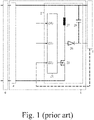
- WO 2010 / 069983 A1 discloses a light emitting diode system for retrofitting fluorescent lighting and discloses at its page 13 lines 9-12 that a problem might occur when two or more of such lamps are used in a series combination.
- WO-2013/136301 discloses a circuit arrangement, a detection circuit and a LED driver circuit for operating at least one lighting unit, such as a LED unit, with a phase-cut operating voltage.
- the circuit arrangement comprising at least an input for receiving a phase-cut operating voltage from said power supply and/or an output for connection to said at least one lighting unit and a pulse injection circuit, configured to determine a phase-cut operation of said power supply and to draw a current pulse from said power supply within a delay time between 200-700 ⁇ s after said phase-cut operation to provide a stable operation of said LED unit with the phase-cut power supply.
- the detection circuit comprises at least an input for receiving a phase-cut operating voltage from said power supply and a lamp compatibility detector, configured to determine the presence of a parallel lamp, connected in parallel with the detection circuit to said phase-cut power supply during operation and to provide a compatibility signal to a LED driver circuit corresponding to the determination of said parallel lamp, so that said driver circuit is set between a normal operating mode and a compatibility mode in dependence of the presence of said parallel lamp.
- WO-2011/117770 discloses a system for controlling a level of light output by a solid state lighting load controlled by a dimmer includes a phase angle detector and a power converter.
- the phase angle detector is configured to detect a phase angle of the dimmer based on a rectified voltage from the dimmer and to determine a power control signal based on comparison of the detected phase angle with a predetermined first threshold.
- the power converter is configured to provide an output voltage to the solid state lighting load, the power converter operating in an open loop mode based on the rectified voltage from the dimmer when the detected phase angle is greater than the first threshold, and operating in a closed loop mode based on the rectified voltage from the dimmer and the determined power control signal from the detection circuit when the detected phase angle is less than the first threshold.
- a device for driving a light source, the device comprising
- a driver drives a light source.
- the driver is operable in different modes.
- An input voltage is supplied to the device.
- a controller detects a value of the input voltage and brings the driver into one of the different modes in response to a detection result.
- the device can distinguish between being placed in a series combination (lower value of the input voltage) and being used solely or in a parallel combination (higher value of the input voltage) and can react to the different situations by selecting a suitable mode for the driver.
- the device can be used solely or in a series combination or in a parallel combination, without a person who is installing (a lamp comprising) the device needing to check the situation. This is a great improvement.
- An embodiment of the device is defined by the different modes comprising a first mode and a second mode, the driver being brought into the first mode in case the value of the input voltage is smaller than a threshold value, and the driver being brought into the second mode in case the value of the input voltage is larger than the threshold value.
- the first mode may be suitable for devices used in a series combination
- the second mode may be suitable for devices used solely or in a parallel combination.
- An embodiment of the device is defined by the first mode comprising a preset-mode and the second mode comprising a feedback-mode.
- the drivers of the devices may start reacting to each other, therefore the first mode should be a preset-mode, without using feedback information from the light source.
- the second mode may be a feedback-mode wherein feedback information from the light source is used.
- An embodiment of the device is defined by a combination of the light source and the driver in the preset-mode showing a substantially constant-resistor-load-behavior.
- drivers that in combinations with light sources show substantially constant-resistor-load-behaviors, will stay stable and will not react to each other.
- An embodiment of the device is defined by the driver comprising a switch that in the preset-mode is operated at a constant conducting time and that in the feedback-mode is operated in response to feedback-information derived from the light source.
- a switch of a driver is operated at a constant conducting time, a combination of the driver and the light source will show a substantially constant-resistor-load-behavior.
- An embodiment of the device is defined by the controller being configured to, at start-up, keep the driver de-activated during a time-interval. When, at start-up, keeping a driver de-activated, a value of an input voltage can be determined better.
- An embodiment of the device is defined by the controller comprising a comparator circuit for comparing the value of the input voltage with a threshold value and for in response to a comparison result producing a first control signal defining the comparison result.
- a comparator circuit is a low cost, simple and robust solution for detecting a value of an input voltage.
- An embodiment of the device is defined by the controller comprising a trigger circuit for in response to a presence of the input voltage producing a second control signal defining a time-interval from start-up during which the driver is to be kept de-activated.
- a trigger circuit is a low cost, simple and robust solution for at start-up defining a time-interval during which a driver is to be kept de-activated.
- a lamp comprising the device as defined above.
- the lamp further comprise a light source.
- the lamp In a first mode the lamp is suitable to be used in a series combination with another lamp, and a second mode the lamp is suitable to be used solely or in a parallel combination with another lamp.
- An embodiment of the lamp is defined by the light source comprising a light emitting diode circuit.
- a light emitting diode circuit comprises one or more light emitting diodes of whatever kind and in whatever combination.
- An embodiment of the device is defined by the lamp being in the form of a retrofit tube.
- a method for controlling a driver for driving a light source the driver being operable in different modes, including a first and a second mode, the method comprising a step of, in response to a detection of a value of an input voltage, that is supplied to the driver, bringing the driver in the first or the second mode, the driver being brought into the first mode in case the value of the input voltage is smaller than a threshold value, and the driver being brought into the second mode in case the value of the input voltage is larger than the threshold value, the first mode comprising a preset-mode and the second mode comprising a feedback-mode.
- a basic idea is that a value of an input voltage may be used to determine a mode of a driver.
- a problem to provide an improved lamp has been solved.
- a further advantage is that, in addition to the fact that a person who is installing the device or the lamp does not need to check the kind of connection, the device is low cost, simple and robust.
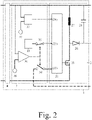
- the device 1 comprises a driver 2 and a rectifier circuit 4. Inputs of the rectifier circuit 4 are coupled to outputs of an optional EMI filter 6 (electromagnetic interference filter). Outputs of the rectifier circuit 4 are coupled to inputs of the driver 2. Outputs of the driver 2 are coupled to terminals of a light source 5.
- EMI filter 6 electromagnetic interference filter
- the driver 2 comprises an interface 21 with a first input 22 for receiving a feedback-signal carrying feedback-information from the light source 5.
- This feedback-information may for example define a value of an amplitude of a current flowing through (a part of) the light source 5 or may for example define a value of an intensity of light coming from (a part of) the light source 5.
- the interface 21 derives / calculates from this feedback-information a value of a conducting time of a switch of the driver 2 at which conducting time a converter 25-28 is to be operated.
- the interface 21 may derive / calculate from this feedback-information a value of a duty cycle or a value of a frequency or a value of a peak current to be delivered or a value of an amount of power to be delivered etc. for example in case other kinds of converters are used.
- An output of the interface 21 is coupled to a control electrode of a switch 25 here in the form of a transistor.
- This switch 25 is conducting during a conducting time (on-time) and is non-conducting during a following non-conducting time (off-time).
- a duty cycle is defined by a combination of the conducting time and the non-conducting time.
- a first main electrode of the switch 25 is coupled via an inductor 27 to a first input and a first output of the driver 2, and a second main electrode of the switch 25 is coupled to a second input of the driver 2.
- the first main electrode of the switch 25 is further coupled via a diode 26 to a second output of the driver 2. Between the first and second outputs of the driver 2, a capacitor 28 is present.
- the components 25-28 form a buck-boost converter, but other kinds of converters are not to be excluded.
- the interface 21 further comprises a second input 23 for receiving a parameter-signal carrying parameter-information and a third input 24 for receiving an on-off-signal carrying on-off-information.
- the driver 2 can be operated in different modes.
- a first mode such as for example a preset-mode
- the driver 2 is operated in response to the parameter-information, such as a fixed value of a conducting time or a fixed value of a duty cycle or a fixed value of a frequency or a fixed value of a peak current to be delivered or a fixed value of an amount of power to be delivered etc. and the feedback-information is ignored.
- a second mode such as for example a feedback-mode
- the parameter-information is ignored and the feedback-information is used for operating the driver 2. So, here in the Fig. 1 , the driver 2 is operated in the feedback-mode.
- the device 1 comprises the driver 2 already shown in and discussed for the Fig. 1 and further comprises a controller 3 located between the rectifier circuit 4 and the driver 2.
- the controller 3 may comprise a comparator circuit 31 having a first input coupled to a first output of the rectifier circuit 4 and having a second input coupled to a first source 36 for comparing a value of a direct-current voltage as supplied by the rectifier circuit 4 with a first threshold value and for in response to a comparison result producing a first control signal defining the comparison result.
- the first control signal is for example used for controlling a first switch 34 and a second switch 35.
- the device 1 forms probably part of a series combination as shown in and discussed for the Fig. 4 .
- the driver 2 should be operated in the preset-mode, and the second switch 35 is brought into a conducting mode, and the parameter-signal as for example generated by a generator 33 is provided to the second input 23 of the interface 21.
- the first switch 34 is brought into a non-conducting mode, and the feedback-signal cannot reach the first input 22 of the interface 21.
- the device 1 is probably solely used or forms probably part of a parallel combination.
- the driver 2 can be operated in the feedback-mode, and the first switch 34 is brought into a conducting mode, and the feedback-signal is provided to the first input 22 of the interface 21.
- the second switch 35 is brought into a non-conducting mode, and the parameter-signal as for example generated by a generator 33 cannot reach the second input 23 of the interface 21.
- the value of the direct-current voltage as supplied by the rectifier circuit 4 is equal to the first threshold value as provided by the first source 36, one of both options may be chosen. Instead of using the switches 34 and 35, it might be possible to activate and de-activate the inputs 22 and 23, or to activate and de-activate the feedback-signal and the parameter-signal.
- the controller 3 may further comprise a trigger circuit 32 for in response to a presence of the direct-current voltage as supplied by the rectifier circuit 4 producing a second control signal defining a time-interval from start-up during which the driver 2 is to be kept de-activated.
- the trigger circuit 32 for example compares a value of a voltage of a serial-resistor-capacitor-network with a second threshold value as provided by the second source 37 and produces an on-signal as soon as the voltage across the capacitor of the serial-resistor-capacitor-network has exceeded the second threshold value. So, at start-up, the driver 2 is kept de-activated during a time-interval such as for example 100 msec. or 200 msec. or 500 msec. etc. to give the comparator circuit 31 time to make a comparison and to select a mode for the driver 2.
- a generator may be used for at start-up generating an off-signal to be supplied to the third input 24 of the interface 21, with the comparator circuit 31 as soon as being ready providing an on-signal to be supplied to the third input 24 of the interface 21 and overruling the off-signal.
- the device 1 comprises a driver 2 for driving a light source 5, which driver 2 is operable in different modes, and comprises a controller 3 for, in response to a detection of a value of an input voltage, that is supplied to the device 1 possibly via an electromagnetic ballast, bringing the driver 2 in one of the different modes.
- the different modes may for example comprise a first mode and a second mode.
- the driver 2 may be brought into the first mode in case the value of the input voltage is smaller than a threshold value.
- the driver 2 may be brought into the second mode in case the value of the input voltage is larger than a threshold value.
- the first mode may comprise a preset-mode and the second mode may comprise a feedback-mode.
- the device 1 may further comprise a rectifier circuit 4 for rectifying an alternating-current voltage into a direct-current voltage.
- the value of the input voltage may be a value of the direct-current voltage.
- the rectifier circuit 4 may be left out, for example in case the driver 2 has an in-built rectifier circuit or in case the driver 2 can handle an alternating-current voltage.
- the controller 3 may have an in-built rectifier circuit or the controller 3 may be able to handle an alternating-current voltage.
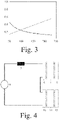
- a characteristic is shown (horizontal axis Volt, vertical axis Ampère) of a combination of a driver 2 and a light source 5 comprising a light emitting diode circuit when showing a substantially constant-resistor-load-behavior (dotted line) and a substantially constant-power-load-behavior (solid line).
- the substantially constant-resistor-load-behavior is to be preferred. This behavior is realized by operating the driver 2 at a fixed value of a conducting time while ignoring the feedback-information.
- the substantially constant-power-load-behavior or a substantially constant-current-load-behavior is to be preferred. This behavior is realized by operating the driver 2 in response to the feedback-information.
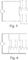
- a first lamp comprises a first EMI filter 6, a first device 1 and a first light source 5 as discussed for the Fig. 1-3
- a second lamp comprises a second EMI filter 16, a second device 11 and a second light source 15 in line with the first ones. Both lamps are coupled serially to each other and the serial combination is coupled via an electromagnetic ballast 7 to a supply 8 such as mains.
- a first lamp comprises a first EMI filter 6, a first device 1 and a first light source 5 as discussed for the Fig. 1-3
- a second lamp comprises a second EMI filter 16, a second device 11 and a second light source 15 in line with the first ones.
- Both lamps are coupled serially to each other and the serial combination is coupled to a supply 8 such as mains, without an electromagnetic ballast being present. Alternatively, such an electromagnetic ballast may be added.
- a first lamp comprises a first EMI filter 6, a first device 1 and a first light source 5 as discussed for the Fig. 1-3
- a second lamp comprises a second EMI filter 16, a second device 11 and a second light source 15 in line with the first ones.
- the first lamp is coupled to a supply 8 such as mains, without an electromagnetic ballast being present.
- a supply 8 such as mains
- an electromagnetic ballast may be added.
- both lamps are present, they are coupled in parallel to each other and the parallel combination is coupled to a supply 8 such as mains, without an electromagnetic ballast being present.
- such an electromagnetic ballast may be added.
- a low pass filter 43 receives the feedback-signal from the light source 5, such as a value of a current flowing through the light source 5, and low pass filters it.
- a generator 41 produces a reference value, and a subtracter 42 subtracts the filtered value from the reference value and supplies a difference value to a compensator 44.
- the compensator 44 supplies a compensated difference value to a first main contact of a third switch 46. This compensated difference value is to be used in the feedback-mode.
- a second main contact of the third switch 46 receives the fixed value of the conducting time to be used in the preset-mode from a generator 45.
- a detector 47 controls the third switch 46 in response to a detection of a value of the input voltage supplied to the device possibly via the electromagnetic ballast.
- a modulator 48 uses the compensated difference value or the fixed value to calculate a pulse width modulation signal and a driving circuit 49 converts this pulse width modulation signal into a driving signal destined for a control electrode of the switch 25.
- the parts 45-47 may form part of the controller 3, and the parts 48 and 49 may form part of the driver 2, with the parts 41-44 for example being external parts.
- the parts 41-44, 46, 48 and 49 may form part of the driver 2, with the parts 45 and 47 forming part of the controller 3.
- only the part 47 may form part of the controller 3, with all other parts forming part of the driver 2.
- the entire controller 3 may form part of the driver 2.
- the controller 3 and the interface 21 may be partly or fully integrated.
- First and second elements can be coupled directly without a third element being in between and can be coupled indirectly via the third element.
- Values of input voltages and values of direct-current voltages may be average values, root-mean-square values, peak values or other kinds of values.
- devices 1 for driving light sources 5 comprise drivers 2 operable in different modes and controllers 3 for, in response to detections of values of input voltages supplied to the devices 1, bringing the drivers 2 in one of the different modes.
- Such devices 1 can be used solely and in series and parallel combinations.
- a first / second mode is selected.
- the first mode is a preset-mode
- the second mode is a feedback-mode.
- a combination of the light source 5 and the driver 2 may show a constant-resistor-load-behavior in the preset-mode.
- the device 2 may comprise a switch 25 that in the preset-mode is operated at a constant conducting time and that in the feedback-mode is operated in response to feedback-information derived from the light source 5. At start-up, the driver 2 may be kept de-activated during a time-interval.
Landscapes
- Circuit Arrangement For Electric Light Sources In General (AREA)
- Arrangement Of Elements, Cooling, Sealing, Or The Like Of Lighting Devices (AREA)
- Non-Portable Lighting Devices Or Systems Thereof (AREA)
Applications Claiming Priority (2)
| Application Number | Priority Date | Filing Date | Title |
|---|---|---|---|
| EP14177356 | 2014-07-17 | ||
| PCT/EP2015/066199 WO2016008943A2 (en) | 2014-07-17 | 2015-07-15 | Driving a light source via different modes |
Publications (2)
| Publication Number | Publication Date |
|---|---|
| EP3170369A2 EP3170369A2 (en) | 2017-05-24 |
| EP3170369B1 true EP3170369B1 (en) | 2022-05-18 |
Family
ID=51178788
Family Applications (1)
| Application Number | Title | Priority Date | Filing Date |
|---|---|---|---|
| EP15736299.7A Active EP3170369B1 (en) | 2014-07-17 | 2015-07-15 | Driving a light source via different modes |
Country Status (5)
| Country | Link |
|---|---|
| US (1) | US10225895B2 (enExample) |
| EP (1) | EP3170369B1 (enExample) |
| JP (1) | JP6646645B2 (enExample) |
| CN (1) | CN106576407B (enExample) |
| WO (1) | WO2016008943A2 (enExample) |
Families Citing this family (3)
| Publication number | Priority date | Publication date | Assignee | Title |
|---|---|---|---|---|
| US10716189B2 (en) * | 2017-02-06 | 2020-07-14 | Signify Holding B.V. | Controller and method for controlling luminaires in a lighting network |
| EP3874910A1 (en) | 2018-10-29 | 2021-09-08 | Signify Holding B.V. | Led lighting driver and drive method |
| EP3915340B1 (en) | 2019-01-25 | 2023-11-22 | Signify Holding B.V. | Lighting driver and drive method |
Citations (2)
| Publication number | Priority date | Publication date | Assignee | Title |
|---|---|---|---|---|
| US20060082316A1 (en) * | 2004-09-14 | 2006-04-20 | Keihin Corporation | Starter drive device |
| US20130334976A1 (en) * | 2012-06-13 | 2013-12-19 | Au Optronics Corp. | Light emitting diode driving circuit and driving method thereof |
Family Cites Families (19)
| Publication number | Priority date | Publication date | Assignee | Title |
|---|---|---|---|---|
| JPH10162964A (ja) * | 1996-12-02 | 1998-06-19 | Sekisui Chem Co Ltd | 照明制御装置 |
| US6936968B2 (en) | 2001-11-30 | 2005-08-30 | Mule Lighting, Inc. | Retrofit light emitting diode tube |
| US8531109B2 (en) | 2008-12-16 | 2013-09-10 | Ledned Holding B.V. | LED tube system |
| US20100264827A1 (en) * | 2009-04-18 | 2010-10-21 | Huang Guo-Jhong | Control Device of Cup Lamp |
| US8310845B2 (en) * | 2010-02-10 | 2012-11-13 | Power Integrations, Inc. | Power supply circuit with a control terminal for different functional modes of operation |
| TW201206248A (en) * | 2010-03-25 | 2012-02-01 | Koninkl Philips Electronics Nv | Method and apparatus for increasing dimming range of solid state lighting fixtures |
| US8242766B2 (en) * | 2010-04-20 | 2012-08-14 | Power Integrations, Inc. | Dimming control for a switching power supply |
| JP2012004093A (ja) * | 2010-05-15 | 2012-01-05 | Saka Techno Science Co Ltd | 直管型照明装置及び製造方法 |
| US8604712B2 (en) | 2010-08-17 | 2013-12-10 | Keystone L.E.D. Holdings Llc | LED luminaires power supply |
| BR112013009250A2 (pt) * | 2010-10-19 | 2020-10-06 | Koninklijke Philips Electronics N.V | disposição do circuito de led, fonte de luz de led para operação em uma disposição do circuito de led e método para operar uma fonte de luz de led conectada por um elemento rativo com uma tensão operacional dc |
| JP5043176B2 (ja) * | 2010-11-02 | 2012-10-10 | 三菱電機株式会社 | 光源点灯装置及び照明器具 |
| JP6532677B2 (ja) * | 2011-05-19 | 2019-06-19 | シグニファイ ホールディング ビー ヴィ | 光発生装置 |
| JP2013037791A (ja) * | 2011-08-04 | 2013-02-21 | Sumitomo Wiring Syst Ltd | 回路基板と端子金具の接続構造 |
| KR101306740B1 (ko) | 2011-08-25 | 2013-09-11 | 엘지전자 주식회사 | 조명 장치 및 조명 장치에서 조사되는 광을 제어하는 방법 |
| JP6190396B2 (ja) * | 2012-03-16 | 2017-08-30 | フィリップス ライティング ホールディング ビー ヴィ | 回路装置 |
| BR112014023013B1 (pt) * | 2012-03-20 | 2021-05-18 | Signify Holding B.V. | conjunto de circuito para controlar pelo menos uma carga; lâmpada de led; e método de controle de pelo menos uma carga com um conjunto de circuito |
| JP2013239347A (ja) * | 2012-05-15 | 2013-11-28 | Panasonic Corp | 点灯装置および照明装置 |
| EP2701461A1 (en) * | 2012-08-24 | 2014-02-26 | Dialog Semiconductor GmbH | Solid state lightening driver with mixed control of power switch |
| US9748858B2 (en) | 2012-09-28 | 2017-08-29 | Osram Sylvania Inc. | Solid state light source driver establishing buck or boost operation |
-
2015
- 2015-07-15 EP EP15736299.7A patent/EP3170369B1/en active Active
- 2015-07-15 US US15/326,257 patent/US10225895B2/en active Active
- 2015-07-15 CN CN201580038924.3A patent/CN106576407B/zh active Active
- 2015-07-15 JP JP2017501645A patent/JP6646645B2/ja active Active
- 2015-07-15 WO PCT/EP2015/066199 patent/WO2016008943A2/en not_active Ceased
Patent Citations (2)
| Publication number | Priority date | Publication date | Assignee | Title |
|---|---|---|---|---|
| US20060082316A1 (en) * | 2004-09-14 | 2006-04-20 | Keihin Corporation | Starter drive device |
| US20130334976A1 (en) * | 2012-06-13 | 2013-12-19 | Au Optronics Corp. | Light emitting diode driving circuit and driving method thereof |
Also Published As
| Publication number | Publication date |
|---|---|
| US20170202064A1 (en) | 2017-07-13 |
| JP6646645B2 (ja) | 2020-02-14 |
| EP3170369A2 (en) | 2017-05-24 |
| WO2016008943A2 (en) | 2016-01-21 |
| CN106576407A (zh) | 2017-04-19 |
| CN106576407B (zh) | 2019-08-16 |
| JP2017520893A (ja) | 2017-07-27 |
| US10225895B2 (en) | 2019-03-05 |
| WO2016008943A3 (en) | 2016-03-31 |
Similar Documents
| Publication | Publication Date | Title |
|---|---|---|
| KR101417538B1 (ko) | 발광 다이오드 램프를 위한 적응 조광 감지 및 제어 | |
| EP2515611B1 (en) | Lighting device and illumination apparatus | |
| US9681503B2 (en) | Transformer for a lamp, LED converter, and transformer operation method | |
| US8508150B2 (en) | Controllers, systems and methods for controlling dimming of light sources | |
| US8581517B2 (en) | Systems and methods for driving a light source | |
| EP2723146B1 (en) | Pulse width modulation control of LEDs | |
| EP2498579A2 (en) | Controllers, systems and methods for controlling dimming of light sources | |
| US20130278145A1 (en) | Circuits and methods for driving light sources | |
| US20120319610A1 (en) | Led lighting apparatus | |
| EP2408266A2 (en) | Circuits and methods for controlling power of light sources | |
| US8049436B2 (en) | Dimmer and lighting apparatus | |
| JP2007080771A (ja) | 照明用低圧電源回路、照明装置および照明用低圧電源出力方法 | |
| US9559675B1 (en) | Current shaping scheme in TRIAC dimmable LED driver | |
| JP5959785B2 (ja) | 電源装置、光源点灯装置およびバッテリ充電装置 | |
| EP3170369B1 (en) | Driving a light source via different modes | |
| JP6023414B2 (ja) | 電源装置及び照明器具 | |
| EP2699060A2 (en) | Luminaire | |
| JP5773786B2 (ja) | 光源点灯装置及び照明器具 | |
| JP6277792B2 (ja) | 点灯装置および照明器具 | |
| JP5645303B2 (ja) | リモート制御ワンコンバータ電源回路 | |
| JP6072488B2 (ja) | 点灯装置及び照明装置 | |
| US10993303B2 (en) | Power supply circuit, lighting system, and method of operating a power supply circuit | |
| JP6533980B2 (ja) | 照明器具 | |
| JP6297130B2 (ja) | 点灯装置及び照明装置 | |
| KR20150143184A (ko) | 플라이백 컨버터 방식의 플리커 프리 led 디밍 장치 |
Legal Events
| Date | Code | Title | Description |
|---|---|---|---|
| STAA | Information on the status of an ep patent application or granted ep patent |
Free format text: STATUS: THE INTERNATIONAL PUBLICATION HAS BEEN MADE |
|
| PUAI | Public reference made under article 153(3) epc to a published international application that has entered the european phase |
Free format text: ORIGINAL CODE: 0009012 |
|
| STAA | Information on the status of an ep patent application or granted ep patent |
Free format text: STATUS: REQUEST FOR EXAMINATION WAS MADE |
|
| 17P | Request for examination filed |
Effective date: 20170217 |
|
| AK | Designated contracting states |
Kind code of ref document: A2 Designated state(s): AL AT BE BG CH CY CZ DE DK EE ES FI FR GB GR HR HU IE IS IT LI LT LU LV MC MK MT NL NO PL PT RO RS SE SI SK SM TR |
|
| AX | Request for extension of the european patent |
Extension state: BA ME |
|
| RIN1 | Information on inventor provided before grant (corrected) |
Inventor name: TAO, HAIMIN |
|
| DAV | Request for validation of the european patent (deleted) | ||
| DAX | Request for extension of the european patent (deleted) | ||
| RAP1 | Party data changed (applicant data changed or rights of an application transferred) |
Owner name: PHILIPS LIGHTING HOLDING B.V. |
|
| RAP1 | Party data changed (applicant data changed or rights of an application transferred) |
Owner name: SIGNIFY HOLDING B.V. |
|
| STAA | Information on the status of an ep patent application or granted ep patent |
Free format text: STATUS: EXAMINATION IS IN PROGRESS |
|
| 17Q | First examination report despatched |
Effective date: 20200115 |
|
| REG | Reference to a national code |
Ref country code: DE Ref legal event code: R079 Ref document number: 602015079048 Country of ref document: DE Free format text: PREVIOUS MAIN CLASS: H05B0033080000 Ipc: H05B0045357000 |
|
| GRAP | Despatch of communication of intention to grant a patent |
Free format text: ORIGINAL CODE: EPIDOSNIGR1 |
|
| STAA | Information on the status of an ep patent application or granted ep patent |
Free format text: STATUS: GRANT OF PATENT IS INTENDED |
|
| RIC1 | Information provided on ipc code assigned before grant |
Ipc: H05B 45/3725 20200101ALI20211124BHEP Ipc: H05B 45/36 20200101ALI20211124BHEP Ipc: H05B 45/357 20200101AFI20211124BHEP |
|
| INTG | Intention to grant announced |
Effective date: 20211213 |
|
| GRAS | Grant fee paid |
Free format text: ORIGINAL CODE: EPIDOSNIGR3 |
|
| GRAA | (expected) grant |
Free format text: ORIGINAL CODE: 0009210 |
|
| STAA | Information on the status of an ep patent application or granted ep patent |
Free format text: STATUS: THE PATENT HAS BEEN GRANTED |
|
| AK | Designated contracting states |
Kind code of ref document: B1 Designated state(s): AL AT BE BG CH CY CZ DE DK EE ES FI FR GB GR HR HU IE IS IT LI LT LU LV MC MK MT NL NO PL PT RO RS SE SI SK SM TR |
|
| REG | Reference to a national code |
Ref country code: GB Ref legal event code: FG4D |
|
| REG | Reference to a national code |
Ref country code: CH Ref legal event code: EP |
|
| REG | Reference to a national code |
Ref country code: IE Ref legal event code: FG4D |
|
| REG | Reference to a national code |
Ref country code: DE Ref legal event code: R096 Ref document number: 602015079048 Country of ref document: DE |
|
| REG | Reference to a national code |
Ref country code: AT Ref legal event code: REF Ref document number: 1493878 Country of ref document: AT Kind code of ref document: T Effective date: 20220615 |
|
| REG | Reference to a national code |
Ref country code: LT Ref legal event code: MG9D |
|
| REG | Reference to a national code |
Ref country code: NL Ref legal event code: MP Effective date: 20220518 |
|
| REG | Reference to a national code |
Ref country code: AT Ref legal event code: MK05 Ref document number: 1493878 Country of ref document: AT Kind code of ref document: T Effective date: 20220518 |
|
| PG25 | Lapsed in a contracting state [announced via postgrant information from national office to epo] |
Ref country code: SE Free format text: LAPSE BECAUSE OF FAILURE TO SUBMIT A TRANSLATION OF THE DESCRIPTION OR TO PAY THE FEE WITHIN THE PRESCRIBED TIME-LIMIT Effective date: 20220518 Ref country code: PT Free format text: LAPSE BECAUSE OF FAILURE TO SUBMIT A TRANSLATION OF THE DESCRIPTION OR TO PAY THE FEE WITHIN THE PRESCRIBED TIME-LIMIT Effective date: 20220919 Ref country code: NO Free format text: LAPSE BECAUSE OF FAILURE TO SUBMIT A TRANSLATION OF THE DESCRIPTION OR TO PAY THE FEE WITHIN THE PRESCRIBED TIME-LIMIT Effective date: 20220818 Ref country code: NL Free format text: LAPSE BECAUSE OF FAILURE TO SUBMIT A TRANSLATION OF THE DESCRIPTION OR TO PAY THE FEE WITHIN THE PRESCRIBED TIME-LIMIT Effective date: 20220518 Ref country code: LT Free format text: LAPSE BECAUSE OF FAILURE TO SUBMIT A TRANSLATION OF THE DESCRIPTION OR TO PAY THE FEE WITHIN THE PRESCRIBED TIME-LIMIT Effective date: 20220518 Ref country code: HR Free format text: LAPSE BECAUSE OF FAILURE TO SUBMIT A TRANSLATION OF THE DESCRIPTION OR TO PAY THE FEE WITHIN THE PRESCRIBED TIME-LIMIT Effective date: 20220518 Ref country code: GR Free format text: LAPSE BECAUSE OF FAILURE TO SUBMIT A TRANSLATION OF THE DESCRIPTION OR TO PAY THE FEE WITHIN THE PRESCRIBED TIME-LIMIT Effective date: 20220819 Ref country code: FI Free format text: LAPSE BECAUSE OF FAILURE TO SUBMIT A TRANSLATION OF THE DESCRIPTION OR TO PAY THE FEE WITHIN THE PRESCRIBED TIME-LIMIT Effective date: 20220518 Ref country code: ES Free format text: LAPSE BECAUSE OF FAILURE TO SUBMIT A TRANSLATION OF THE DESCRIPTION OR TO PAY THE FEE WITHIN THE PRESCRIBED TIME-LIMIT Effective date: 20220518 Ref country code: BG Free format text: LAPSE BECAUSE OF FAILURE TO SUBMIT A TRANSLATION OF THE DESCRIPTION OR TO PAY THE FEE WITHIN THE PRESCRIBED TIME-LIMIT Effective date: 20220818 Ref country code: AT Free format text: LAPSE BECAUSE OF FAILURE TO SUBMIT A TRANSLATION OF THE DESCRIPTION OR TO PAY THE FEE WITHIN THE PRESCRIBED TIME-LIMIT Effective date: 20220518 |
|
| PG25 | Lapsed in a contracting state [announced via postgrant information from national office to epo] |
Ref country code: RS Free format text: LAPSE BECAUSE OF FAILURE TO SUBMIT A TRANSLATION OF THE DESCRIPTION OR TO PAY THE FEE WITHIN THE PRESCRIBED TIME-LIMIT Effective date: 20220518 Ref country code: PL Free format text: LAPSE BECAUSE OF FAILURE TO SUBMIT A TRANSLATION OF THE DESCRIPTION OR TO PAY THE FEE WITHIN THE PRESCRIBED TIME-LIMIT Effective date: 20220518 Ref country code: LV Free format text: LAPSE BECAUSE OF FAILURE TO SUBMIT A TRANSLATION OF THE DESCRIPTION OR TO PAY THE FEE WITHIN THE PRESCRIBED TIME-LIMIT Effective date: 20220518 Ref country code: IS Free format text: LAPSE BECAUSE OF FAILURE TO SUBMIT A TRANSLATION OF THE DESCRIPTION OR TO PAY THE FEE WITHIN THE PRESCRIBED TIME-LIMIT Effective date: 20220918 |
|
| PG25 | Lapsed in a contracting state [announced via postgrant information from national office to epo] |
Ref country code: SM Free format text: LAPSE BECAUSE OF FAILURE TO SUBMIT A TRANSLATION OF THE DESCRIPTION OR TO PAY THE FEE WITHIN THE PRESCRIBED TIME-LIMIT Effective date: 20220518 Ref country code: SK Free format text: LAPSE BECAUSE OF FAILURE TO SUBMIT A TRANSLATION OF THE DESCRIPTION OR TO PAY THE FEE WITHIN THE PRESCRIBED TIME-LIMIT Effective date: 20220518 Ref country code: RO Free format text: LAPSE BECAUSE OF FAILURE TO SUBMIT A TRANSLATION OF THE DESCRIPTION OR TO PAY THE FEE WITHIN THE PRESCRIBED TIME-LIMIT Effective date: 20220518 Ref country code: EE Free format text: LAPSE BECAUSE OF FAILURE TO SUBMIT A TRANSLATION OF THE DESCRIPTION OR TO PAY THE FEE WITHIN THE PRESCRIBED TIME-LIMIT Effective date: 20220518 Ref country code: DK Free format text: LAPSE BECAUSE OF FAILURE TO SUBMIT A TRANSLATION OF THE DESCRIPTION OR TO PAY THE FEE WITHIN THE PRESCRIBED TIME-LIMIT Effective date: 20220518 Ref country code: CZ Free format text: LAPSE BECAUSE OF FAILURE TO SUBMIT A TRANSLATION OF THE DESCRIPTION OR TO PAY THE FEE WITHIN THE PRESCRIBED TIME-LIMIT Effective date: 20220518 |
|
| REG | Reference to a national code |
Ref country code: DE Ref legal event code: R097 Ref document number: 602015079048 Country of ref document: DE |
|
| PG25 | Lapsed in a contracting state [announced via postgrant information from national office to epo] |
Ref country code: MC Free format text: LAPSE BECAUSE OF FAILURE TO SUBMIT A TRANSLATION OF THE DESCRIPTION OR TO PAY THE FEE WITHIN THE PRESCRIBED TIME-LIMIT Effective date: 20220518 |
|
| REG | Reference to a national code |
Ref country code: CH Ref legal event code: PL |
|
| PLBE | No opposition filed within time limit |
Free format text: ORIGINAL CODE: 0009261 |
|
| STAA | Information on the status of an ep patent application or granted ep patent |
Free format text: STATUS: NO OPPOSITION FILED WITHIN TIME LIMIT |
|
| REG | Reference to a national code |
Ref country code: BE Ref legal event code: MM Effective date: 20220731 |
|
| PG25 | Lapsed in a contracting state [announced via postgrant information from national office to epo] |
Ref country code: AL Free format text: LAPSE BECAUSE OF FAILURE TO SUBMIT A TRANSLATION OF THE DESCRIPTION OR TO PAY THE FEE WITHIN THE PRESCRIBED TIME-LIMIT Effective date: 20220518 |
|
| 26N | No opposition filed |
Effective date: 20230221 |
|
| PG25 | Lapsed in a contracting state [announced via postgrant information from national office to epo] |
Ref country code: LU Free format text: LAPSE BECAUSE OF NON-PAYMENT OF DUE FEES Effective date: 20220715 Ref country code: LI Free format text: LAPSE BECAUSE OF NON-PAYMENT OF DUE FEES Effective date: 20220731 Ref country code: CH Free format text: LAPSE BECAUSE OF NON-PAYMENT OF DUE FEES Effective date: 20220731 |
|
| PG25 | Lapsed in a contracting state [announced via postgrant information from national office to epo] |
Ref country code: SI Free format text: LAPSE BECAUSE OF FAILURE TO SUBMIT A TRANSLATION OF THE DESCRIPTION OR TO PAY THE FEE WITHIN THE PRESCRIBED TIME-LIMIT Effective date: 20220518 Ref country code: BE Free format text: LAPSE BECAUSE OF NON-PAYMENT OF DUE FEES Effective date: 20220731 |
|
| P01 | Opt-out of the competence of the unified patent court (upc) registered |
Effective date: 20230425 |
|
| PG25 | Lapsed in a contracting state [announced via postgrant information from national office to epo] |
Ref country code: IE Free format text: LAPSE BECAUSE OF NON-PAYMENT OF DUE FEES Effective date: 20220715 |
|
| PG25 | Lapsed in a contracting state [announced via postgrant information from national office to epo] |
Ref country code: IT Free format text: LAPSE BECAUSE OF FAILURE TO SUBMIT A TRANSLATION OF THE DESCRIPTION OR TO PAY THE FEE WITHIN THE PRESCRIBED TIME-LIMIT Effective date: 20220518 |
|
| PG25 | Lapsed in a contracting state [announced via postgrant information from national office to epo] |
Ref country code: HU Free format text: LAPSE BECAUSE OF FAILURE TO SUBMIT A TRANSLATION OF THE DESCRIPTION OR TO PAY THE FEE WITHIN THE PRESCRIBED TIME-LIMIT; INVALID AB INITIO Effective date: 20150715 |
|
| PG25 | Lapsed in a contracting state [announced via postgrant information from national office to epo] |
Ref country code: MK Free format text: LAPSE BECAUSE OF FAILURE TO SUBMIT A TRANSLATION OF THE DESCRIPTION OR TO PAY THE FEE WITHIN THE PRESCRIBED TIME-LIMIT Effective date: 20220511 Ref country code: CY Free format text: LAPSE BECAUSE OF FAILURE TO SUBMIT A TRANSLATION OF THE DESCRIPTION OR TO PAY THE FEE WITHIN THE PRESCRIBED TIME-LIMIT Effective date: 20220511 |
|
| PG25 | Lapsed in a contracting state [announced via postgrant information from national office to epo] |
Ref country code: TR Free format text: LAPSE BECAUSE OF FAILURE TO SUBMIT A TRANSLATION OF THE DESCRIPTION OR TO PAY THE FEE WITHIN THE PRESCRIBED TIME-LIMIT Effective date: 20220511 |
|
| PG25 | Lapsed in a contracting state [announced via postgrant information from national office to epo] |
Ref country code: MT Free format text: LAPSE BECAUSE OF FAILURE TO SUBMIT A TRANSLATION OF THE DESCRIPTION OR TO PAY THE FEE WITHIN THE PRESCRIBED TIME-LIMIT Effective date: 20220511 |
|
| PG25 | Lapsed in a contracting state [announced via postgrant information from national office to epo] |
Ref country code: BG Free format text: LAPSE BECAUSE OF FAILURE TO SUBMIT A TRANSLATION OF THE DESCRIPTION OR TO PAY THE FEE WITHIN THE PRESCRIBED TIME-LIMIT Effective date: 20220518 |
|
| PG25 | Lapsed in a contracting state [announced via postgrant information from national office to epo] |
Ref country code: BG Free format text: LAPSE BECAUSE OF FAILURE TO SUBMIT A TRANSLATION OF THE DESCRIPTION OR TO PAY THE FEE WITHIN THE PRESCRIBED TIME-LIMIT Effective date: 20220518 |
|
| PGFP | Annual fee paid to national office [announced via postgrant information from national office to epo] |
Ref country code: DE Payment date: 20250926 Year of fee payment: 11 |
|
| PGFP | Annual fee paid to national office [announced via postgrant information from national office to epo] |
Ref country code: GB Payment date: 20250722 Year of fee payment: 11 |
|
| PGFP | Annual fee paid to national office [announced via postgrant information from national office to epo] |
Ref country code: FR Payment date: 20250725 Year of fee payment: 11 |