EP3169136A1 - Datenverarbeitungssystem - Google Patents
Datenverarbeitungssystem Download PDFInfo
- Publication number
- EP3169136A1 EP3169136A1 EP16754741.3A EP16754741A EP3169136A1 EP 3169136 A1 EP3169136 A1 EP 3169136A1 EP 16754741 A EP16754741 A EP 16754741A EP 3169136 A1 EP3169136 A1 EP 3169136A1
- Authority
- EP
- European Patent Office
- Prior art keywords
- processing group
- delay unit
- timing signal
- processor
- unit
- Prior art date
- Legal status (The legal status is an assumption and is not a legal conclusion. Google has not performed a legal analysis and makes no representation as to the accuracy of the status listed.)
- Granted
Links
Images


Classifications
-
- G—PHYSICS
- G06—COMPUTING OR CALCULATING; COUNTING
- G06F—ELECTRIC DIGITAL DATA PROCESSING
- G06F30/00—Computer-aided design [CAD]
- G06F30/30—Circuit design
- G06F30/35—Delay-insensitive circuit design, e.g. asynchronous or self-timed
-
- H—ELECTRICITY
- H04—ELECTRIC COMMUNICATION TECHNIQUE
- H04B—TRANSMISSION
- H04B1/00—Details of transmission systems, not covered by a single one of groups H04B3/00 - H04B13/00; Details of transmission systems not characterised by the medium used for transmission
- H04B1/06—Receivers
- H04B1/16—Circuits
-
- H—ELECTRICITY
- H04—ELECTRIC COMMUNICATION TECHNIQUE
- H04L—TRANSMISSION OF DIGITAL INFORMATION, e.g. TELEGRAPHIC COMMUNICATION
- H04L1/00—Arrangements for detecting or preventing errors in the information received
- H04L1/0001—Systems modifying transmission characteristics according to link quality, e.g. power backoff
- H04L1/0023—Systems modifying transmission characteristics according to link quality, e.g. power backoff characterised by the signalling
- H04L1/0027—Scheduling of signalling, e.g. occurrence thereof
-
- H—ELECTRICITY
- H04—ELECTRIC COMMUNICATION TECHNIQUE
- H04W—WIRELESS COMMUNICATION NETWORKS
- H04W88/00—Devices specially adapted for wireless communication networks, e.g. terminals, base stations or access point devices
- H04W88/08—Access point devices
Definitions
- the present invention relates to the data processing field, and in particular, to a data processing system.
- a base station After receiving a high frequency signal by using an antenna of a receiving device, a base station needs to convert the high frequency signal to an intermediate frequency signal, and then processes service data in the intermediate frequency signal, so that processed service data can meet a system requirement of the receiving device.
- a hardware system is used to process service data.
- the hardware system includes a timing signal generation unit, N hardware units, and (N-1) delay units.
- the timing signal generation unit is hardwired to both the 1 st hardware unit and the 1 st delay unit.
- the i th hardware unit is hardwired to the (i+1) th hardware unit.
- the i th delay unit is hardwired to both the (i+1) th hardware unit and the (i+1) th delay unit.
- N and i are positive integers, and N>i>1.
- the timing signal generation unit sends a generated first timing signal to the 1 st hardware unit and the 1 st delay unit by using a hardwire.
- the 1 st delay unit delays the timing signal, and sends an obtained second timing signal to the 2 nd hardware unit and the 2 nd delay unit by using a hardwire.
- the 1 st hardware unit processes original service data according to obtained control information, and under triggering of the first timing signal, sends obtained first service data and the control information to the 2 nd hardware unit by using a hardwire.
- the 2 nd hardware unit processes the first service data according to the control information, and sends obtained second service data to the 3 rd hardware unit by using a hardwire under triggering of the second timing signal.
- a hardware unit has a limited service data processing capability. Therefore, when large quantities of operations are required for service data, efficiency of processing the service data by using a hardware system is relatively low.
- embodiments of the present invention provide a data processing system.
- the technical solutions are as follows:
- an output interface in the i th processing group is hardwired to a hardware unit in the (i+1) th processing group, and a second delay unit in the i th processing group is hardwired to a third delay unit in the (i+1) th processing group, where i is a positive integer.
- an output interface in the i th processing group is hardwired to an input interface in the (i+1) th processing group, and a second delay unit in the i th processing group is hardwired to a first delay unit in the (i+1) th processing group, where i is a positive integer.
- the output interface in the i th processing group is hardwired to a processor in the (i+1) th processing group
- the second delay unit in the i th processing group is hardwired to the processor in the (i+1) th processing group
- the processor in the (i+1) th processing group is configured to: generate control information according to a control signal from the output interface in the i th processing group and a second timing signal from the second delay unit in the i th processing group, and process service data from the output interface in the i th processing group according to the control information.
- a hardware unit in the i th processing group is hardwired to a hardware unit in the (i+1) th processing group
- a third delay unit in the i th processing group is hardwired to a third delay unit in the (i+1) th processing group, where i is a positive integer.
- a hardware unit in the i th processing group is hardwired to an input interface in the (i+1) th processing group, and a third delay unit in the i th processing group is hardwired to a first delay unit in the (i+1) th processing group, where i is a positive integer.
- the hardware unit in the i th processing group is hardwired to a processor in the (i+1) th processing group
- the third delay unit in the i th processing group is hardwired to the processor in the (i+1) th processing group
- the processor in the (i+1) th processing group is configured to: generate control information according to a control signal from the hardware unit in the i th processing group and a third timing signal from the third delay unit in the i th processing group, and process service data from the hardware unit in the i th processing group according to the control information.
- the first possible implementation manner of the first aspect, the second possible implementation manner of the first aspect, the third possible implementation manner of the first aspect, the fourth possible implementation manner of the first aspect, the fifth possible implementation manner of the first aspect, or the sixth possible implementation manner of the first aspect in a seventh possible implementation manner of the first aspect, there is at least one processor in a soft processing group of the a soft processing groups, the soft processing group further includes a fourth delay unit, the fourth delay unit is hardwired to both the first delay unit and each processor, and the fourth delay unit is configured to: delay the first timing signal that is from the first delay unit, to obtain a fourth timing signal, and send the fourth timing signal to each processor; and the processor is specifically configured to process the service data according to the control information in the first data packet under triggering of the fourth timing signal.
- the soft processing group further includes a fourth delay unit and a timing scheduling unit, the fourth delay unit is hardwired to both the first delay unit and the timing scheduling unit, the timing scheduling unit is hardwired to each processor, the fourth delay unit is configured to: delay the first timing signal that is from the first delay unit, to obtain a fourth timing signal, and send the fourth timing signal to the timing scheduling unit, and the timing scheduling unit is configured to: delay the fourth timing signal that is from the fourth delay unit, to obtain a fifth timing signal, and send the fifth timing signal to each processor; and the processor is specifically configured to process the service data according to the control information in the first data packet under triggering of the
- the input interface is further configured to:
- the first delay unit in the i th processing group is a timing signal generation unit, and the timing signal generation unit is configured to generate the first timing signal.
- a soft processing group including a processor is disposed in a data processing system, so that service data involving a large quantity of operations in a processing process may be sent to the processor for processing. Because the processor has a relatively strong processing capability, a problem of low service data processing efficiency of a hardware system resulting from a relatively weak processing capability of a hard processing group is resolved, and service data processing efficiency is improved.
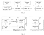
- FIG. 2 shows a structural block diagram of a data processing system provided in an embodiment of the present invention.
- the data processing system includes N cascaded processing groups.
- Each soft processing group 210 includes a first delay unit 211, an input interface 212, a processor 213, an output interface 214, and a second delay unit 215.
- the first delay unit 211 is hardwired to both the input interface 212 and the second delay unit 215.
- the processor 213 is electrically connected to both the input interface 212 and the output interface 214.
- the second delay unit 215 is hardwired to the output interface 214.
- the first delay unit 211 is configured to send a first timing signal to the input interface 212 and the second delay unit 215.
- the second delay unit 215 is configured to: delay the first timing signal that is from the first delay unit 211, to obtain a second timing signal, and send the second timing signal to the output interface 214.
- the input interface 212 is configured to: obtain service data, control information, and the first timing signal, combine the service data and the control information under triggering of the first timing signal to obtain a first data packet, and send the first data packet to the processor 213.
- the processor 213 is configured to: process the service data according to the control information in the first data packet, and send an obtained second data packet to the output interface 214, where the second data packet includes processed service data.
- the output interface 214 is configured to: parse the second data packet to obtain the processed service data, obtain the second timing signal, and output the processed service data under triggering of the second timing signal.
- Each hard processing group 220 includes a third delay unit 221 and a hardware unit 222.
- the third delay unit 221 is hardwired to the hardware unit 222.
- the third delay unit 221 is configured to send a third timing signal to the hardware unit 222.
- N, a, and b are all positive integers.
- the processor 213 is a component that implements functions by executing code, and the functions implemented by the processor 213 may be changed by modifying code.
- the processor 213 may include an algorithm unit and a memory.
- the algorithm unit may be a central processing unit (full name in English: Central Processing Unit, CPU for short), a processor for implementing digital signal processing (full name in English: Digital Signal Processing, DSP for short), or the like.
- the hardware unit 222 is a component that implements functions by using a circuit connection. After a circuit connection relationship is definite, the functions that can be implemented by the hardware unit 222 are definite.
- the processor 213 can identify a data packet, and the hardware unit 222 can send or receive service data by using a hardwire.
- the input interface 212 is configured to obtain a data packet according to service data that is input by using a hardwire.
- the output interface 214 is configured to: parse the data packet to obtain the service data, and send, by using a hardwire, the service data obtained by means of parsing.
- the hardwire is a physical wire.
- the service data is data, in an intermediate frequency signal, for implementing a service.
- a delay unit may further be disposed in a processing group, and a timing signal generated by using the delay unit is used to control an output time point.
- the first delay unit 211 is configured to send the first timing signal to the input interface 212.
- the first timing signal is used to control an output time point of the input interface 212.
- the second delay unit 215 is configured to: delay the first timing signal that is from the first delay unit 211 by a pre-determined time length, and send the second timing signal obtained by means of delay to the output interface 214.
- the second timing signal is used to control an output time point of the output interface 214.
- the pre-determined time length is greater than or equal to a maximum time length for processing a data packet by the processor 213.
- the third delay unit 221 is configured to send the third timing signal to the hardware unit 222.
- the third timing signal is used to control an output time point of the hardware unit 222.
- the first timing signal may be generated by the first delay unit 211 or may be obtained by delaying a received timing signal by the first delay unit 211
- the third timing signal may be generated by the third delay unit 221 or may be obtained by delaying a received timing signal by the third delay unit 221. These are not limited in this embodiment.
- the service data is data, in the intermediate frequency signal, for implementing a service.
- the control information is used to indicate a service data processing manner of a processor.
- the control information is used to indicate an algorithm for the service data, or the control information is used to indicate a time point of an operation for the service data.
- the control information and the service data are synchronized.
- the processor 213 can identify a data packet, and the hardware unit 222 can send or receive service data by using a hardwire. Therefore, if data communication needs to be implemented between the processor 213 and the hardware unit 222, the input interface 212 further needs to be disposed before the processor 213.
- the input interface 212 is configured to combine the service data and the control information that are input by using a hardwire to obtain the first data packet.
- the first timing signal is used to indicate a time point at which the input interface 212 sends the first data packet.
- the input interface 212 when a soft processing group is the 1 st processing group in the data processing system, receives the service data and the control information. In this case, a first timing signal is generated by the first delay unit 211.
- the service data and the control information are generated by a previous processing group connected to the soft processing group.
- the processing group may be a soft processing group or a hard processing group.
- the first timing signal is obtained by the first delay unit 211 by delaying a timing signal sent by the previous processing group.
- the hardware unit 222 served as input of the data processing system, receives the service data.
- the third timing signal is generated by the third delay unit 221.
- the service data is generated by a previous processing group connected to the hard processing group.
- the processing group may be a soft processing group or a hard processing group.
- the third timing signal is obtained by the third delay unit 221 by delaying a timing signal sent by the previous processing group.
- the processor 213 may start a data processing procedure under triggering of the first data packet.
- the processor 213 can process the first data packet in real time. Therefore, a time length for processing the first data packet is shortened, and service data processing efficiency is improved.
- the processor 213 may read information, such as a packet validity signal, control information, and a packet number, from a control information packet. When determining that the packet validity signal is a pre-determined packet validity flag value, the processor 213 determines that the control information packet is valid and a service data packet corresponding to the control information packet has been stored in a specified storage area.
- the processor 213 obtains, from the specified storage area, the service data packet whose packet number is the same as that of the control information packet, reads service data from the service data packet, and processes the service data according to the control information. After processing the service data, the processor removes the packet validity signal.
- the processor 213 needs to complete processing of the first data packet within a fixed time period, and the fixed time length is a maximum time length for processing one first data packet by the processor 213.
- the processor 213 may add the processed service data to the second data packet, and send the second data packet to the output interface 214; or may add the processed service data and the control information to the second data packet, and send the second data packet to the output interface 214.
- the second timing signal is used to indicate a time point at which the output interface 214 sends a processed service data packet, and may be obtained by the second delay unit 215 by delaying the first timing signal delay unit by a pre-determined time length.
- the pre-determined time length is greater than or equal to the maximum time length for processing the first data packet by the processor 213, so as to ensure that the output interface 214 can output the processed service data in the second data packet.
- the second timing signal is obtained by delaying the first delay signal. Therefore, a fixed delay time between the input interface 212 and the output interface 214 can be ensured, thereby ensuring a fixed total delay time of the data processing system.
- a soft processing group including a processor is disposed in the data processing system, so that service data involving a large quantity of operations in a processing process may be sent to the processor for processing. Because the processor has a relatively strong processing capability, a problem of low service data processing efficiency of a hardware system resulting from a relatively weak processing capability of a hard processing group is resolved, and service data processing efficiency is improved.
- a second delay unit triggers an output interface to output data, ensuring a fixed time length for processing service data by the soft processing group, and ensuring a fixed total delay time of the data processing system.
- another embodiment of the present invention further provides a data processing system.
- Internal structures of a soft processing group and a hard processing group are different. Therefore, a cascade between a soft processing group and a hard processing group, a cascade between a soft processing group and a soft processing group, a cascade between a hard processing group and a soft processing group, and a cascade between a hard processing group and a hard processing group are all different.
- the following uses the i th processing group and the (i+1) th processing group as an example to detail the foregoing four cascading relationships, where i is a positive integer.
- a processor 213 When processing service data according to the foregoing cascading relationships, a processor 213 needs to determine a service data processing manner according to control information, where the control information and the service data are synchronized.
- the synchronization between the control information and the service data means a sampling period of the service data is the same as that of the control information. Assuming that the sampling period of the service data includes P sampling points, the sampling period of the control information also includes the P sampling points. Therefore, the i th processing group may sample a control signal, to obtain control information synchronous with service data, and send the control information and the service data together to the (i+1) th soft processing group. Generally, a change frequency of the control signal is lower than that of the service data.
- a sampling frequency of the control signal may be lower than that of the service data, so as to avoid redundant control information.
- a higher sampling frequency indicates higher precision of the control information.
- a larger data volume in the control information results in more resources to be consumed for sending the control information.
- the input interface 212 is further configured to: generate a service data packet within the n th segment of a pre-determined period, and add the service data at a first data sampling rate to the service data packet, where the pre-determined period includes m coherent segments; generate a control information packet within the n th segment, and add the control information at a second data sampling rate to the control information packet; obtain the n th portion of the first data packet by adding the control information packet to the corresponding service data packet; and send the first data packet to the processor, where m is a positive integer, and n is a positive integer variable between 1 and m. Therefore, service data packets within all segments constitute a to-be-output service data packet.
- the first data packet may include a service data packet and a control data packet, and the control information packet is sent after the service data packet.
- Service data is added to the service data packet
- control information is added to the control data packet.
- a control signal may be sampled within a pre-determined period, to obtain m control information packets.
- the pre-determined period includes m coherent segments.
- one service data packet and one control information packet are generated.
- a control information packet is added to a corresponding service data packet.
- One service data packet and one control information packet are served as one portion of the first data packet together.
- the first data packet sequentially includes: the 1 st service data packet, the 1 st control information packet, the 2 nd service data packet, and the 2 nd control information packet.
- the 1 st service data packet is obtained by sampling service data within the 1 st segment
- the 1 st control information packet is obtained by sampling a control signal within the 1 st segment.
- the 2 nd service data packet is obtained by sampling service data within the 2 nd segment
- the 2 nd control information is obtained by sampling a control signal within the 2 nd segment.
- the first data packet includes only one service data packet and one control information packet.
- the control signal when a control signal is being sampled, and when the control signal is a pulse signal: if a rising edge exists in the control signal within a pre-determined period, the control information is set to 1; or if a rising edge does not exist in the control signal within a pre-determined period, the control information is set to 0.
- the control signal is a level signal: if the control signal retains to a high level within a pre-detennined period, the control information is set to 1; or if the control signal retains to a low level within a pre-determined period, the control information is set to 0.
- the control signal may also be sampled in another manner, which is not limited in this embodiment.
- the i th processing group may directly send a control signal to a processor 213 in the (i+1) th soft processing group by using a hardwire.
- the processor 213 in the (i+1) th soft processing group further needs to obtain a timing signal sent by the i th processing group, so as to generate, according to the timing signal, control information synchronous with service data.
- the timing signal is the second timing signal.
- the timing signal is the third timing signal.
- an output interface 214 in the i th processing group is hardwired to a processor 213 in the (i+1) th processing group
- a second delay unit 215 in the i th processing group is hardwired to the processor 213 in the (i+1) th processing group.
- the processor 213 in the (i+1) th processing group is configured to: generate control information according to a control signal from the output interface 214 in the i th processing group and a second timing signal from the second delay unit 215 in the i th processing group, and process service data from the output interface 214 in the i th processing group according to the control information.
- the output interface 214 in the i th processing group sends the control signal to the processor 213 in the (i+1) th processing group.
- the second delay unit 215 in the i th processing group sends the second timing signal to the processor 213 in the (i+1) th processing group.
- the processor 213 in the (i+1) th processing group generates the control information according to the control signal and the second timing signal, and process the service data according to the control information.
- a hardware unit 222 in the i th processing group is hardwired to a processor 213 in the (i+1) th processing group
- a third delay unit 221 in the i th processing group is hardwired to the processor 213 in the (i+1) th processing group.
- the processor 213 in the (i+1) th processing group is configured to: generate control information according to a control signal from the hardware unit 222 in the i th processing group and a third timing signal from the third delay unit 221 in the i th processing group, and process service data from the hardware unit 222 in the i th processing group according to the control information.
- the hardware unit 222 in the i th processing group sends the control signal to the processor 213 in the (i+1) th processing group.
- the third delay unit 221 in the i th processing group sends the third timing signal to the processor 213 in the (i+1) th processing group.
- the processor 213 in the (i+1) th processing group generates the control information according to the control signal and the third timing signal, and process the service data according to the control information.
- an input interface 212 is further configured to: obtain service data and a first timing signal, combine the service data and the control information under triggering of the first timing signal to obtain a first data packet, and send the first data packet to the processor 213.
- the processor 213 is further configured to: obtain a control signal and the first timing signal, generate, according to the control signal and under triggering of the first timing signal, control information synchronous with the service data, process the service data in the first data packet according to the control information, and send an obtained second data packet to an output interface 214, where the second data packet includes processed service data.
- the output interface 214 is further configured to: parse the second data packet to obtain the processed service data, obtain a second timing signal, and output the processed service data under triggering of the second timing signal.
- the input interface 212 is specifically configured to: generate a service data packet, add the service data at a pre-determined data sampling rate to the first data packet within a pre-determined period, and send the first data packet to the processor 213.
- the processor 213 is specifically configured to: obtain the pre-determined period, the pre-determined data sampling rate, and a generation time point of the first data packet, and sample the control signal at the pre-determined data sampling rate within the pre-determined period starting from the generation time point, to obtain the control information synchronous with the service data.
- the processor 213 needs to ensure that a process of sampling the control signal is synchronized with a process of sampling the service data by the input interface 212, so as to ensure complete synchronization between the generated control information and the service data.
- the processor 213 needs to obtain a sampling start time point, a sampling rate, and a sampling period that are of the service data.
- the sampling start time point is the generation time point of the first data packet.
- the sampling rate is the pre-determined data sampling rate.
- the sampling period is the pre-determined period.
- the processor 213 may sample, based on the generation time point, the control signal at the pre-determined data sampling rate within the pre-determined period, to obtain the control information.
- the processor 213 may further generate a control information packet for the control information.
- a packet number of the control information packet is the same as a packet number of the first data packet.
- the processor 213 obtains the control information packet whose packet number is the same as that of the first data packet, and processes the first data packet according to the control information packet.
- a soft processing group of a soft processing groups includes one processor 213, the processor 213 is electrically connected to both an input interface 212 and an output interface 214.
- the processor 213 may be electrically connected to the other processors 213, and may be electrically connected to an input interfaced 212 or an output interface 214.
- the processor 213 may start a data processing process after obtaining a data packet.
- the processor 213 may start a data processing process under triggering of a timing signal, and in this case, the timing signal needs to be sent to the processor 213 by using a hardwire.
- the timing signal is sent to the processor 213 by using a hardwire in the following two manners.
- the soft processing group further includes a fourth delay unit 216.
- the fourth delay unit 216 is hardwired to both a first delay unit 211 and each processor 213.
- the fourth delay unit 216 is configured to: delay a first timing signal that is from the first delay unit 211, to obtain a fourth timing signal, and send the fourth timing signal to each processor 213.
- the processor 213 is specifically configured to process the service data according to the control information in the first data packet under triggering of the fourth timing signal.
- the first delay unit 211 sends the first timing signal to the fourth delay unit 216.
- the fourth delay unit 216 determines a delay time of each processor 213 according to a pre-determined policy, and after delaying the first timing signal by the corresponding delay time, sends the fourth timing signal obtained by means of delaying to the corresponding processor 213.
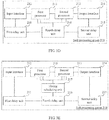
- the fourth timing signal is used to control a time point at which the corresponding processor 213 processes the first data packet. Referring to a schematic diagram of first-type timing scheduling of a processor shown in FIG. 3D , in FIG. 3D , an example in which a soft processing group 210 includes a first processor 213 and a second processor 213 is used for description.
- the soft processing group includes the first processor 213 and the second processor 213.
- a delay time corresponding to the first processor 213 is 10s, and a delay time corresponding to the second processor 213 is 20 seconds.
- the fourth delay unit 216 determines that the fourth timing signal is to be sent to the first processor 213 at a time point 16:02:25, and that the fourth timing signal is to be sent to the second processor 213 at a time point 16:02:35.
- a processor 213 may include at least two functional components
- the fourth delay unit 216 may be hardwired to each functional component of the processor 213.
- the processor 213 includes a CPU and a DSP, and the fourth delay unit 216 is connected to the CPU by using a hardwire and connected to the DSP by using another hardwire. If the functional components need to be controlled separately, at least two fourth timing signals need to be generated for the processor 213, and each fourth timing signal is sent, by using a corresponding hardwire, to a corresponding functional component of the processor 213.
- the soft processing group further includes a fourth delay unit 216 and a timing scheduling unit 217.
- the fourth delay unit 216 is hardwired to both a first delay unit 211 and the timing scheduling unit 217.
- the timing scheduling unit 217 is hardwired to each processor 213.
- the fourth delay unit 216 is configured to: delay a first timing signal that is from the first delay unit 211, to obtain a fourth timing signal, and send the fourth timing signal to the timing scheduling unit 217.
- the timing scheduling unit 217 is configured to: delay the fourth timing signal that is from the fourth delay unit 216, to obtain a fifth timing signal, and send the fifth timing signal to each processor 213.
- the processor 213 is specifically configured to process the service data according to the control information in the first data packet under triggering of the fifth timing signal.
- the first delay unit 211 sends the first timing signal to the fourth delay unit 216.
- the fourth delay unit 216 sends the fourth timing signal obtained by means of delaying to the timing scheduling unit 217.
- the timing scheduling unit 217 determines a delay time of each processor 213 according to a pre-determined policy, and after delaying the fourth timing signal by the corresponding delay time, sends the fifth timing signal obtained by means of delaying to the corresponding processor 213.
- the fifth timing signal is used to control a time point at which the corresponding processor 213 processes the first data packet.
- a processor 213 may include at least two functional components
- the timing scheduling unit 217 may be hardwired to each functional component of the processor 213.
- the processor 213 includes a CPU and a DSP, and the timing scheduling unit 217 is connected to the CPU by using a hardwire and connected to the DSP by using another hardwire. If the functional components need to be controlled separately, at least two fifth timing signals need to be generated for the processor 213, and each fifth timing signal is sent, by using a corresponding hardwire, to a corresponding functional component of the processor 213.
- a second delay unit 215 is connected to the first delay unit 211, and a time length for which the second delay unit 215 delays the first timing signal that is sent by the first delay unit 211 is greater than a time length for which the fourth delay unit 216 delays the first timing signal that is sent by the first delay unit 211.
- a second delay unit 215 is connected to the fourth delay unit 216, and delays the fourth timing signal that is sent by the fourth delay unit 216.
- the first delay unit 211 when frequencies of clock sources used by the first delay unit 211 and the second delay unit 215 are the same, the first delay unit 211 sends a first timing signal to a synchronization delay unit 218.
- the synchronization delay unit 218 sends a first timing signal obtained after synchronization processing to the second delay unit 215.
- frequencies of clock sources used by the first delay unit 211 and the second delay unit 215 are different, that is, the first delay unit 211 and the second delay unit 215 are asynchronous, the first delay unit 211 sends a first timing signal to an asynchronization delay unit 219.
- the asynchronization delay unit 219 sends a first timing signal obtained after asynchronization processing to the second delay unit 215. This ensures that the data processing system is free of variation after the data processing system is powered on.
- the synchronization delay unit 218 and the asynchronization delay unit 219 both can be implemented by using the prior art, and details are not described herein. Similarly, the synchronization delay unit 218 and the asynchronization delay unit 219 can also be used for a delay between the first delay unit 211 and the fourth delay unit 216, and details are not described herein.
- FIG. 3G a hard processing group 220, a soft processing group 210, and a hard processing group 220 that are sequentially connected are included.
- a third delay unit 221 in the 1 st hard processing group 220 is a timing signal generation unit 221.
- a soft processing group including a processor is disposed in the data processing system, so that service data involving a large quantity of operations in a processing process may be sent to the processor for processing. Because the processor has a relatively strong processing capability, a problem of low service data processing efficiency of a hardware system resulting from a relatively weak processing capability of a hard processing group is resolved, and service data processing efficiency is improved.
- a second delay unit triggers an output interface to output data, ensuring a fixed time length for processing service data by the soft processing group, and ensuring a fixed total delay time of the data processing system.
- a control signal and a timing signal are sent to a processor by using a hardwire, and the processor generates, according to the control signal and the timing signal, control information synchronous with service data. This not only meets a real-time requirement for the control information, but also reduces resources consumed for sending the control information.
- sequence numbers of the foregoing embodiments of the present invention are merely for illustrative purposes, and are not intended to indicate priorities of the embodiments.
- a person of ordinary skill in the art may understand that all or some of the steps of the embodiments may be implemented by hardware or a program instructing related hardware.
- the program may be stored in a computer-readable storage medium.
- the storage medium may include: a read-only memory, a magnetic disk, or an optical disc.
Landscapes
- Engineering & Computer Science (AREA)
- Signal Processing (AREA)
- Computer Networks & Wireless Communication (AREA)
- Theoretical Computer Science (AREA)
- Computer Hardware Design (AREA)
- Physics & Mathematics (AREA)
- Evolutionary Computation (AREA)
- General Physics & Mathematics (AREA)
- General Engineering & Computer Science (AREA)
- Geometry (AREA)
- Quality & Reliability (AREA)
- Information Transfer Systems (AREA)
- Mobile Radio Communication Systems (AREA)
Applications Claiming Priority (2)
| Application Number | Priority Date | Filing Date | Title |
|---|---|---|---|
| CN201510091317.5A CN104735824B (zh) | 2015-02-28 | 2015-02-28 | 数据处理系统 |
| PCT/CN2016/073303 WO2016134632A1 (zh) | 2015-02-28 | 2016-02-03 | 数据处理系统 |
Publications (3)
| Publication Number | Publication Date |
|---|---|
| EP3169136A1 true EP3169136A1 (de) | 2017-05-17 |
| EP3169136A4 EP3169136A4 (de) | 2017-08-09 |
| EP3169136B1 EP3169136B1 (de) | 2018-10-03 |
Family
ID=53459139
Family Applications (1)
| Application Number | Title | Priority Date | Filing Date |
|---|---|---|---|
| EP16754741.3A Active EP3169136B1 (de) | 2015-02-28 | 2016-02-03 | Datenverarbeitungssystem |
Country Status (4)
| Country | Link |
|---|---|
| US (1) | US20170337316A1 (de) |
| EP (1) | EP3169136B1 (de) |
| CN (1) | CN104735824B (de) |
| WO (1) | WO2016134632A1 (de) |
Families Citing this family (2)
| Publication number | Priority date | Publication date | Assignee | Title |
|---|---|---|---|---|
| CN104735824B (zh) * | 2015-02-28 | 2018-03-13 | 华为技术有限公司 | 数据处理系统 |
| KR102895283B1 (ko) * | 2020-12-02 | 2025-12-03 | 현대자동차주식회사 | 차량 방전 유발 제어기 식별 시스템 |
Family Cites Families (8)
| Publication number | Priority date | Publication date | Assignee | Title |
|---|---|---|---|---|
| JP3672874B2 (ja) * | 2002-01-25 | 2005-07-20 | Necマイクロシステム株式会社 | データ処理装置 |
| ATE554443T1 (de) * | 2003-06-25 | 2012-05-15 | Koninkl Philips Electronics Nv | Anweisungsgesteuerte datenverarbeitungseinrichtung und -verfahren |
| CN101123597A (zh) * | 2007-07-06 | 2008-02-13 | 北京天碁科技有限公司 | 一种终端基带处理装置 |
| WO2009065255A1 (en) * | 2007-11-21 | 2009-05-28 | Lucent Technologies Inc. | Cdma base station and signal processing method used therein |
| WO2009113014A2 (en) * | 2008-03-10 | 2009-09-17 | Nxp B.V. | Data processing system |
| US8627175B2 (en) * | 2010-09-27 | 2014-01-07 | Seagate Technology Llc | Opportunistic decoding in memory systems |
| US9053232B2 (en) * | 2012-12-14 | 2015-06-09 | Altera Corporation | Method and apparatus for supporting a unified debug environment |
| CN104735824B (zh) * | 2015-02-28 | 2018-03-13 | 华为技术有限公司 | 数据处理系统 |
-
2015
- 2015-02-28 CN CN201510091317.5A patent/CN104735824B/zh active Active
-
2016
- 2016-02-03 EP EP16754741.3A patent/EP3169136B1/de active Active
- 2016-02-03 WO PCT/CN2016/073303 patent/WO2016134632A1/zh not_active Ceased
-
2017
- 2017-08-09 US US15/673,005 patent/US20170337316A1/en not_active Abandoned
Also Published As
| Publication number | Publication date |
|---|---|
| CN104735824B (zh) | 2018-03-13 |
| US20170337316A1 (en) | 2017-11-23 |
| CN104735824A (zh) | 2015-06-24 |
| EP3169136A4 (de) | 2017-08-09 |
| WO2016134632A1 (zh) | 2016-09-01 |
| EP3169136B1 (de) | 2018-10-03 |
Similar Documents
| Publication | Publication Date | Title |
|---|---|---|
| EP4047934B1 (de) | Verfahren und vorrichtung zum senden von nachrichten, lesbares medium und elektronische vorrichtung | |
| US9465404B2 (en) | Timing synchronization circuit for wireless communication apparatus | |
| CN111399588B (zh) | 时钟信号产生电路、驱动方法及电子设备 | |
| EP3407145B1 (de) | Fpga-basierter rechteckwellengenerator und verfahren zur erzeugung von rechteckwellen | |
| EP3197054A1 (de) | Dynamisches taktumschaltungsverfahren und vorrichtung sowie computerlesbares medium | |
| CN109032498B (zh) | 一种多fpga的多通道采集系统的波形量化同步方法 | |
| PH12019502679A1 (en) | Information determination method, terminal apparatus, amd network apparatus | |
| WO2018186876A1 (en) | Technologies for high-precision timestamping of packets | |
| CN113204514A (zh) | 一种提高芯片的spi接口频率的方法 | |
| KR20150013491A (ko) | 차동 클럭 신호 생성기 | |
| EP3751382B1 (de) | Sequenzsignalgenerator und sequenzsignalerzeugungsverfahren | |
| EP3169136A1 (de) | Datenverarbeitungssystem | |
| CN114285514A (zh) | 一种时钟同步方法和装置 | |
| CN114328347A (zh) | 一种提高spi总线频率的方法 | |
| CN104348465B (zh) | 一种控制方法和控制电路 | |
| WO2017173915A1 (zh) | 一种报文处理方法、装置、系统和计算机存储介质 | |
| CN104350758A (zh) | 信号处理装置和信号处理方法 | |
| CN111221378B (zh) | 周期信号的时钟域转换方法、装置及可读存储介质 | |
| US10128818B2 (en) | Data processor, data processing method and communication device | |
| JP2013009332A5 (de) | ||
| CN116827335A (zh) | 一种分频装置及数据处理电路 | |
| EP2928082A1 (de) | Taktaktivierungsschaltung | |
| JP3719413B2 (ja) | データ伝送システム及びそれに用いられるデータ送受信装置と、その方法 | |
| CN112988631A (zh) | 一种基于现场可编程门阵列的数据处理方法及装置 | |
| CN113472565B (zh) | 服务器功能的扩容方法、装置、设备和计算机可读介质 |
Legal Events
| Date | Code | Title | Description |
|---|---|---|---|
| STAA | Information on the status of an ep patent application or granted ep patent |
Free format text: STATUS: THE INTERNATIONAL PUBLICATION HAS BEEN MADE |
|
| PUAI | Public reference made under article 153(3) epc to a published international application that has entered the european phase |
Free format text: ORIGINAL CODE: 0009012 |
|
| STAA | Information on the status of an ep patent application or granted ep patent |
Free format text: STATUS: REQUEST FOR EXAMINATION WAS MADE |
|
| 17P | Request for examination filed |
Effective date: 20170209 |
|
| AK | Designated contracting states |
Kind code of ref document: A1 Designated state(s): AL AT BE BG CH CY CZ DE DK EE ES FI FR GB GR HR HU IE IS IT LI LT LU LV MC MK MT NL NO PL PT RO RS SE SI SK SM TR |
|
| AX | Request for extension of the european patent |
Extension state: BA ME |
|
| A4 | Supplementary search report drawn up and despatched |
Effective date: 20170706 |
|
| RIC1 | Information provided on ipc code assigned before grant |
Ipc: H04W 88/08 20090101AFI20170630BHEP |
|
| GRAP | Despatch of communication of intention to grant a patent |
Free format text: ORIGINAL CODE: EPIDOSNIGR1 |
|
| STAA | Information on the status of an ep patent application or granted ep patent |
Free format text: STATUS: GRANT OF PATENT IS INTENDED |
|
| INTG | Intention to grant announced |
Effective date: 20180417 |
|
| DAV | Request for validation of the european patent (deleted) | ||
| DAX | Request for extension of the european patent (deleted) | ||
| GRAS | Grant fee paid |
Free format text: ORIGINAL CODE: EPIDOSNIGR3 |
|
| GRAA | (expected) grant |
Free format text: ORIGINAL CODE: 0009210 |
|
| STAA | Information on the status of an ep patent application or granted ep patent |
Free format text: STATUS: THE PATENT HAS BEEN GRANTED |
|
| AK | Designated contracting states |
Kind code of ref document: B1 Designated state(s): AL AT BE BG CH CY CZ DE DK EE ES FI FR GB GR HR HU IE IS IT LI LT LU LV MC MK MT NL NO PL PT RO RS SE SI SK SM TR |
|
| REG | Reference to a national code |
Ref country code: GB Ref legal event code: FG4D |
|
| REG | Reference to a national code |
Ref country code: CH Ref legal event code: EP Ref country code: AT Ref legal event code: REF Ref document number: 1050098 Country of ref document: AT Kind code of ref document: T Effective date: 20181015 |
|
| REG | Reference to a national code |
Ref country code: IE Ref legal event code: FG4D Ref country code: DE Ref legal event code: R096 Ref document number: 602016006258 Country of ref document: DE |
|
| REG | Reference to a national code |
Ref country code: NL Ref legal event code: MP Effective date: 20181003 |
|
| REG | Reference to a national code |
Ref country code: LT Ref legal event code: MG4D |
|
| REG | Reference to a national code |
Ref country code: AT Ref legal event code: MK05 Ref document number: 1050098 Country of ref document: AT Kind code of ref document: T Effective date: 20181003 |
|
| PG25 | Lapsed in a contracting state [announced via postgrant information from national office to epo] |
Ref country code: NL Free format text: LAPSE BECAUSE OF FAILURE TO SUBMIT A TRANSLATION OF THE DESCRIPTION OR TO PAY THE FEE WITHIN THE PRESCRIBED TIME-LIMIT Effective date: 20181003 |
|
| PG25 | Lapsed in a contracting state [announced via postgrant information from national office to epo] |
Ref country code: IS Free format text: LAPSE BECAUSE OF FAILURE TO SUBMIT A TRANSLATION OF THE DESCRIPTION OR TO PAY THE FEE WITHIN THE PRESCRIBED TIME-LIMIT Effective date: 20190203 Ref country code: FI Free format text: LAPSE BECAUSE OF FAILURE TO SUBMIT A TRANSLATION OF THE DESCRIPTION OR TO PAY THE FEE WITHIN THE PRESCRIBED TIME-LIMIT Effective date: 20181003 Ref country code: BG Free format text: LAPSE BECAUSE OF FAILURE TO SUBMIT A TRANSLATION OF THE DESCRIPTION OR TO PAY THE FEE WITHIN THE PRESCRIBED TIME-LIMIT Effective date: 20190103 Ref country code: LT Free format text: LAPSE BECAUSE OF FAILURE TO SUBMIT A TRANSLATION OF THE DESCRIPTION OR TO PAY THE FEE WITHIN THE PRESCRIBED TIME-LIMIT Effective date: 20181003 Ref country code: NO Free format text: LAPSE BECAUSE OF FAILURE TO SUBMIT A TRANSLATION OF THE DESCRIPTION OR TO PAY THE FEE WITHIN THE PRESCRIBED TIME-LIMIT Effective date: 20190103 Ref country code: CZ Free format text: LAPSE BECAUSE OF FAILURE TO SUBMIT A TRANSLATION OF THE DESCRIPTION OR TO PAY THE FEE WITHIN THE PRESCRIBED TIME-LIMIT Effective date: 20181003 Ref country code: AT Free format text: LAPSE BECAUSE OF FAILURE TO SUBMIT A TRANSLATION OF THE DESCRIPTION OR TO PAY THE FEE WITHIN THE PRESCRIBED TIME-LIMIT Effective date: 20181003 Ref country code: ES Free format text: LAPSE BECAUSE OF FAILURE TO SUBMIT A TRANSLATION OF THE DESCRIPTION OR TO PAY THE FEE WITHIN THE PRESCRIBED TIME-LIMIT Effective date: 20181003 Ref country code: PL Free format text: LAPSE BECAUSE OF FAILURE TO SUBMIT A TRANSLATION OF THE DESCRIPTION OR TO PAY THE FEE WITHIN THE PRESCRIBED TIME-LIMIT Effective date: 20181003 Ref country code: HR Free format text: LAPSE BECAUSE OF FAILURE TO SUBMIT A TRANSLATION OF THE DESCRIPTION OR TO PAY THE FEE WITHIN THE PRESCRIBED TIME-LIMIT Effective date: 20181003 Ref country code: LV Free format text: LAPSE BECAUSE OF FAILURE TO SUBMIT A TRANSLATION OF THE DESCRIPTION OR TO PAY THE FEE WITHIN THE PRESCRIBED TIME-LIMIT Effective date: 20181003 |
|
| PG25 | Lapsed in a contracting state [announced via postgrant information from national office to epo] |
Ref country code: PT Free format text: LAPSE BECAUSE OF FAILURE TO SUBMIT A TRANSLATION OF THE DESCRIPTION OR TO PAY THE FEE WITHIN THE PRESCRIBED TIME-LIMIT Effective date: 20190203 Ref country code: AL Free format text: LAPSE BECAUSE OF FAILURE TO SUBMIT A TRANSLATION OF THE DESCRIPTION OR TO PAY THE FEE WITHIN THE PRESCRIBED TIME-LIMIT Effective date: 20181003 Ref country code: SE Free format text: LAPSE BECAUSE OF FAILURE TO SUBMIT A TRANSLATION OF THE DESCRIPTION OR TO PAY THE FEE WITHIN THE PRESCRIBED TIME-LIMIT Effective date: 20181003 Ref country code: RS Free format text: LAPSE BECAUSE OF FAILURE TO SUBMIT A TRANSLATION OF THE DESCRIPTION OR TO PAY THE FEE WITHIN THE PRESCRIBED TIME-LIMIT Effective date: 20181003 Ref country code: GR Free format text: LAPSE BECAUSE OF FAILURE TO SUBMIT A TRANSLATION OF THE DESCRIPTION OR TO PAY THE FEE WITHIN THE PRESCRIBED TIME-LIMIT Effective date: 20190104 |
|
| REG | Reference to a national code |
Ref country code: DE Ref legal event code: R097 Ref document number: 602016006258 Country of ref document: DE |
|
| PG25 | Lapsed in a contracting state [announced via postgrant information from national office to epo] |
Ref country code: IT Free format text: LAPSE BECAUSE OF FAILURE TO SUBMIT A TRANSLATION OF THE DESCRIPTION OR TO PAY THE FEE WITHIN THE PRESCRIBED TIME-LIMIT Effective date: 20181003 Ref country code: DK Free format text: LAPSE BECAUSE OF FAILURE TO SUBMIT A TRANSLATION OF THE DESCRIPTION OR TO PAY THE FEE WITHIN THE PRESCRIBED TIME-LIMIT Effective date: 20181003 |
|
| PLBE | No opposition filed within time limit |
Free format text: ORIGINAL CODE: 0009261 |
|
| STAA | Information on the status of an ep patent application or granted ep patent |
Free format text: STATUS: NO OPPOSITION FILED WITHIN TIME LIMIT |
|
| PG25 | Lapsed in a contracting state [announced via postgrant information from national office to epo] |
Ref country code: SM Free format text: LAPSE BECAUSE OF FAILURE TO SUBMIT A TRANSLATION OF THE DESCRIPTION OR TO PAY THE FEE WITHIN THE PRESCRIBED TIME-LIMIT Effective date: 20181003 Ref country code: EE Free format text: LAPSE BECAUSE OF FAILURE TO SUBMIT A TRANSLATION OF THE DESCRIPTION OR TO PAY THE FEE WITHIN THE PRESCRIBED TIME-LIMIT Effective date: 20181003 Ref country code: RO Free format text: LAPSE BECAUSE OF FAILURE TO SUBMIT A TRANSLATION OF THE DESCRIPTION OR TO PAY THE FEE WITHIN THE PRESCRIBED TIME-LIMIT Effective date: 20181003 Ref country code: SK Free format text: LAPSE BECAUSE OF FAILURE TO SUBMIT A TRANSLATION OF THE DESCRIPTION OR TO PAY THE FEE WITHIN THE PRESCRIBED TIME-LIMIT Effective date: 20181003 |
|
| REG | Reference to a national code |
Ref country code: DE Ref legal event code: R119 Ref document number: 602016006258 Country of ref document: DE |
|
| 26N | No opposition filed |
Effective date: 20190704 |
|
| REG | Reference to a national code |
Ref country code: CH Ref legal event code: PL |
|
| PG25 | Lapsed in a contracting state [announced via postgrant information from national office to epo] |
Ref country code: SI Free format text: LAPSE BECAUSE OF FAILURE TO SUBMIT A TRANSLATION OF THE DESCRIPTION OR TO PAY THE FEE WITHIN THE PRESCRIBED TIME-LIMIT Effective date: 20181003 Ref country code: MC Free format text: LAPSE BECAUSE OF FAILURE TO SUBMIT A TRANSLATION OF THE DESCRIPTION OR TO PAY THE FEE WITHIN THE PRESCRIBED TIME-LIMIT Effective date: 20181003 Ref country code: LU Free format text: LAPSE BECAUSE OF NON-PAYMENT OF DUE FEES Effective date: 20190203 |
|
| REG | Reference to a national code |
Ref country code: BE Ref legal event code: MM Effective date: 20190228 |
|
| REG | Reference to a national code |
Ref country code: IE Ref legal event code: MM4A |
|
| PG25 | Lapsed in a contracting state [announced via postgrant information from national office to epo] |
Ref country code: CH Free format text: LAPSE BECAUSE OF NON-PAYMENT OF DUE FEES Effective date: 20190228 Ref country code: LI Free format text: LAPSE BECAUSE OF NON-PAYMENT OF DUE FEES Effective date: 20190228 |
|
| PG25 | Lapsed in a contracting state [announced via postgrant information from national office to epo] |
Ref country code: DE Free format text: LAPSE BECAUSE OF NON-PAYMENT OF DUE FEES Effective date: 20190903 Ref country code: IE Free format text: LAPSE BECAUSE OF NON-PAYMENT OF DUE FEES Effective date: 20190203 |
|
| PG25 | Lapsed in a contracting state [announced via postgrant information from national office to epo] |
Ref country code: FR Free format text: LAPSE BECAUSE OF NON-PAYMENT OF DUE FEES Effective date: 20190228 Ref country code: BE Free format text: LAPSE BECAUSE OF NON-PAYMENT OF DUE FEES Effective date: 20190228 |
|
| PG25 | Lapsed in a contracting state [announced via postgrant information from national office to epo] |
Ref country code: TR Free format text: LAPSE BECAUSE OF FAILURE TO SUBMIT A TRANSLATION OF THE DESCRIPTION OR TO PAY THE FEE WITHIN THE PRESCRIBED TIME-LIMIT Effective date: 20181003 |
|
| PG25 | Lapsed in a contracting state [announced via postgrant information from national office to epo] |
Ref country code: MT Free format text: LAPSE BECAUSE OF NON-PAYMENT OF DUE FEES Effective date: 20190203 |
|
| PG25 | Lapsed in a contracting state [announced via postgrant information from national office to epo] |
Ref country code: CY Free format text: LAPSE BECAUSE OF FAILURE TO SUBMIT A TRANSLATION OF THE DESCRIPTION OR TO PAY THE FEE WITHIN THE PRESCRIBED TIME-LIMIT Effective date: 20181003 |
|
| PG25 | Lapsed in a contracting state [announced via postgrant information from national office to epo] |
Ref country code: HU Free format text: LAPSE BECAUSE OF FAILURE TO SUBMIT A TRANSLATION OF THE DESCRIPTION OR TO PAY THE FEE WITHIN THE PRESCRIBED TIME-LIMIT; INVALID AB INITIO Effective date: 20160203 |
|
| PG25 | Lapsed in a contracting state [announced via postgrant information from national office to epo] |
Ref country code: MK Free format text: LAPSE BECAUSE OF FAILURE TO SUBMIT A TRANSLATION OF THE DESCRIPTION OR TO PAY THE FEE WITHIN THE PRESCRIBED TIME-LIMIT Effective date: 20181003 |
|
| PGFP | Annual fee paid to national office [announced via postgrant information from national office to epo] |
Ref country code: GB Payment date: 20250102 Year of fee payment: 10 |