EP3161969B1 - Skew control for three-phase communication - Google Patents
Skew control for three-phase communication Download PDFInfo
- Publication number
- EP3161969B1 EP3161969B1 EP15730899.0A EP15730899A EP3161969B1 EP 3161969 B1 EP3161969 B1 EP 3161969B1 EP 15730899 A EP15730899 A EP 15730899A EP 3161969 B1 EP3161969 B1 EP 3161969B1
- Authority
- EP
- European Patent Office
- Prior art keywords
- branch
- signal
- common mode
- signal branch
- voltage
- Prior art date
- Legal status (The legal status is an assumption and is not a legal conclusion. Google has not performed a legal analysis and makes no representation as to the accuracy of the status listed.)
- Active
Links
Images


Classifications
-
- H—ELECTRICITY
- H04—ELECTRIC COMMUNICATION TECHNIQUE
- H04B—TRANSMISSION
- H04B1/00—Details of transmission systems, not covered by a single one of groups H04B3/00 - H04B13/00; Details of transmission systems not characterised by the medium used for transmission
- H04B1/02—Transmitters
- H04B1/04—Circuits
- H04B1/0475—Circuits with means for limiting noise, interference or distortion
-
- H—ELECTRICITY
- H04—ELECTRIC COMMUNICATION TECHNIQUE
- H04B—TRANSMISSION
- H04B3/00—Line transmission systems
- H04B3/02—Details
- H04B3/30—Reducing interference caused by unbalanced currents in a normally balanced line
-
- H—ELECTRICITY
- H04—ELECTRIC COMMUNICATION TECHNIQUE
- H04B—TRANSMISSION
- H04B15/00—Suppression or limitation of noise or interference
- H04B15/02—Reducing interference from electric apparatus by means located at or near the interfering apparatus
-
- H—ELECTRICITY
- H04—ELECTRIC COMMUNICATION TECHNIQUE
- H04L—TRANSMISSION OF DIGITAL INFORMATION, e.g. TELEGRAPHIC COMMUNICATION
- H04L25/00—Baseband systems
- H04L25/02—Details ; arrangements for supplying electrical power along data transmission lines
- H04L25/0264—Arrangements for coupling to transmission lines
- H04L25/028—Arrangements specific to the transmitter end
-
- H—ELECTRICITY
- H04—ELECTRIC COMMUNICATION TECHNIQUE
- H04L—TRANSMISSION OF DIGITAL INFORMATION, e.g. TELEGRAPHIC COMMUNICATION
- H04L25/00—Baseband systems
- H04L25/02—Details ; arrangements for supplying electrical power along data transmission lines
- H04L25/03—Shaping networks in transmitter or receiver, e.g. adaptive shaping networks
- H04L25/03878—Line equalisers; line build-out devices
Definitions
- the technology of the disclosure relates generally to supporting digital cameras in communication devices and, more particularly, to supporting the digital cameras using the MIPI® Alliance camera serial interface (CSI).
- CSI camera serial interface
- Mobile communication devices have become increasingly common in current society. The prevalence of these mobile communication devices is driven in part by the many functions that are now enabled on such devices. Increased processing capabilities in such devices means that mobile communication devices have evolved from being purely communication tools into sophisticated mobile entertainment centers, thus enabling enhanced user experiences.
- Digital imaging is deemed by many end users as one of the most critical features in mobile communication devices.
- highly sophisticated digital camera sensors are integrated into the mobile communication devices to provide higher resolution and better sensitivity in digital imaging applications.
- raw digital data associated with the digital images are transmitted from the digital camera sensor to an image processor for further processing and rendering.
- the raw digital data may be distorted due to inter-symbol interference (ISI), reflections, and crosstalk caused by lossy transmission lines.
- ISI inter-symbol interference
- the mobile communication devices are unable to produce high quality digital images despite having the highly sophisticated digital camera sensors.
- US 2009/058480 describes a multi-phase transmitter configured to change impedance to provide skew control.
- US 2012/146686 describes a transmitter for reducing signal loss in transmission lines by detecting a transition in a data stream, adjusting a source determination resistance and obtaining a gain from the adjusted source determination resistance.
- skew control for three-phase communication may be supported in mobile communication devices using the MIPI® Alliance three-phase camera serial interface (CSI-3) specification.
- a three-phase communication involves three signal branches.
- a signal skew may occur when one signal branch is being coupled to a common mode voltage while another signal branch is being decoupled from the common mode voltage.
- an impedance mismatch is introduced in the signal branch being coupled to the common mode voltage to help shift a rightmost crossing of the signal skew leftward.
- a current source or a current sink is coupled to the signal branch being decoupled from the common mode voltage to help shift a leftmost crossing of the signal skew rightward. More specifically, the current source or the current sink is coupled to the signal branch if the signal branch is switched from the common mode voltage to a lower voltage or a higher voltage. By shifting the rightmost crossing leftward and the leftmost crossing rightward, it is possible to reduce the signal skew, thus leading to reduced jitter and improved data integrity in the three-phase communication.
- a three-phase transmitter comprises a first signal branch, a second signal branch, and a third signal branch.
- Each of the first signal branch, the second signal branch, and the third signal branch comprises a respective branch impedance and a respective driving impedance. If a signal branch among the first signal branch, the second signal branch, and the third signal branch is selected to function as a common mode branch by being coupled to a common mode voltage, the three-phase transmitter is configured to configure the respective driving impedance of the selected signal branch to be less than the respective branch impedance of the selected signal branch.
- a method for reducing signal skew in a three-phase transmitter comprises identifying a signal branch among a first signal branch, a second signal branch, and a third signal branch of a three-phase transmitter, wherein the signal branch is selected to function as a common mode branch by being coupled to a common mode voltage.
- the method also comprises configuring a respective driving impedance of the selected signal branch to be less than a respective branch impedance of the selected signal branch.
- skew control for three-phase communication may be supported in mobile communication devices using the MIPI® Alliance three-phase camera serial interface (CSI-3) specification.
- a three-phase communication involves three signal branches.
- a signal skew may occur when one signal branch is being coupled to a common mode voltage while another signal branch is being decoupled from the common mode voltage.
- an impedance mismatch is introduced in the signal branch being coupled to the common mode voltage to help shift a rightmost crossing of the signal skew leftward.
- a current source or a current sink is coupled to the signal branch being decoupled from the common mode voltage to help shift a leftmost crossing of the signal skew rightward. More specifically, the current source or the current sink is coupled to the signal branch if the signal branch is switched from the common mode voltage to a lower voltage or a higher voltage. By shifting the rightmost crossing leftward and the leftmost crossing rightward, it is possible to reduce the signal skew, thus leading to reduced jitter and improved data integrity in the three-phase communication.
- a brief overview of a conventional three-phase transmitter which may, in a non-limiting example, be used in a camera as part of the CSI-3 specification
- an illustration of signal skew associated with the conventional three-phase transmitter are provided in Figures 1 , 2A , and 2B .
- the discussion of specific exemplary aspects of the skew control for three-phase communication starts below with reference to Figure 3 .
- a time T X and a time T Y are referenced hereinafter to represent a present time and a future time, respectively.
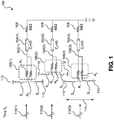
- FIG. 1 is a schematic diagram of an exemplary conventional three-phase transmitter 100 according to the MIPI@ Alliance three-phase camera serial interface (CSI-3) specification.
- the conventional three-phase transmitter 100 comprises a first signal branch 102(1), a second signal branch 102(2), and a third signal branch 102(3).
- the first signal branch 102(1), the second signal branch 102(2), and the third signal branch 102(3) include respective branch impedances 104(1)-104(3) and respective driving impedances 106(1)-106(3).
- each of the respective branch impedances 104(1)-104(3) equals fifty ohms (50 ⁇ ).
- the first signal branch 102(1), the second signal branch 102(2), and the third signal branch 102(3) are each terminated by a 50 ⁇ resistor 108.
- Each of the respective driving impedances 106(1)-106(3) includes a first resistor (R 1 ) and a second resistor (R 2 ) disposed in a parallel arrangement.
- the R 1 and R 2 have one hundred ohms (100 ⁇ ) resistances.
- Each of the first signal branch 102(1), the second signal branch 102(2), and the third signal branch 102(3) can be coupled selectively to an upper mode voltage 110, a lower mode voltage 112, or a common mode voltage 114 by a switch S U and/or a switch S L .
- the upper mode voltage 110, the lower mode voltage 112, or the common mode voltage 114 are three hundred millivolts (300mV), one hundred millivolts (100mV), and two hundred millivolts (200mV), respectively.
- the settings of the switch S U and the switch S L in the first signal branch 102(1), the second signal branch 102(2), and the third signal branch 102(3) are driven by a first branch signal 116(1), a second branch signal 116(2), and a third branch signal 116(3), respectively.
- the first signal branch 102(1), the second signal branch 102(2), and the third signal branch 102(3) are coupled to the upper mode voltage 110, the common mode voltage 114, and the lower mode voltage 112, respectively, at the time T X .
- the switch S L of the first signal branch 102(1) is closed and the switch S U of the first signal branch 102(1) is opened.
- the respective driving impedance 106(1) is determined by the R 2 .
- the switch S U of the second signal branch 102(2) is closed and the switch S L of the second signal branch 102(2) is opened.
- the second signal branch 102(2) is transitioning out of a common mode and the respective driving impedance 106(2) is determined by the R 1 .
- the switch S L and the switch S U of the third signal branch 102(3) are both closed.
- the third signal branch 102(3) is transitioning into the common mode and functions as a common mode branch.
- the respective driving impedance 106(3) is determined by the R 1 and the R 2 that are disposed in a parallel arrangement. Given that the resistances of the R 1 and the R 2 are both 100 ⁇ , the respective driving impedance 106(3) is 50 ⁇ and matches the respective branch impedance 104(3) of the third signal branch 102(3).
- Figure 2A is an exemplary plot 200 illustrating one aspect of a signal skew 202 produced by the conventional three-phase transmitter 100 of Figure 1 .
- Elements of Figure 1 are referenced in connection with Figure 2A and will not be re-described herein.
- a signal skew refers to the difference between propagation delays of any two signals at identical transitions.
- the first signal branch 102(1), the second signal branch 102(2) and the third signal branch 102(3) are respectively coupled to the upper mode voltage 110, the common mode voltage 114, and the lower mode voltage 112 by the first branch signal 116(1), the second branch signal 116(2), and the third branch signal 116(3).
- the first branch signal 116(1), the second branch signal 116(2), and the third branch signal 116(3) respectively cause the first signal branch 102(1), the second signal branch 102(2), and the third signal branch 102(3) to be coupled to the lower mode voltage 112, the upper mode voltage 110, and the common mode voltage 114.
- the third signal branch 102(3) transitions into the common mode and becomes the common mode branch while the second signal branch 102(2) is transitioning out of the common mode.
- the signal skew 202 is defined by a leftmost crossing 204 and a rightmost crossing 206.
- the leftmost crossing 204 is determined by the second signal branch 102(2) that transitions out of (or leaves) the common mode and the rightmost crossing 206 is determined by the third signal branch 102(3) that transitions into (or enters) the common mode.
- the signal skew 202 can cause signal distortions and consequently data losses in the conventional three-phase transmitter 100 of Figure 1 .
- a reduced signal skew 202' can be achieved in the conventional three-phase transmitter 100 of Figure 1 .
- Figure 2B is an exemplary plot 208 illustrating another aspect of the signal skew 202 produced by the conventional three-phase transmitter 100 of Figure 1 .
- the first signal branch 102(1), the second signal branch 102(2), and the third signal branch 102(3) are respectively coupled to the upper mode voltage 110, the lower mode voltage 112, and the common mode voltage 114 by the first branch signal 116(1), the second branch signal 116(2), and the third branch signal 116(3).
- the first branch signal 116(1), the second branch signal 116(2), and the third branch signal 116(3) respectively cause the first signal branch 102(1), the second signal branch 102(2), and the third signal branch 102(3) to be coupled to the common mode voltage 114, the upper mode voltage 110, and the lower mode voltage 112.
- the first signal branch 102(1) is transitioning into the common mode and becoming the common mode branch while the third signal branch 102(3) is transitioning out of the common mode.
- the signal skew 202 may be reduced to the reduced signal skew 202' by shifting the leftmost crossing 204 rightward to the new leftmost crossing 204' and shifting the rightmost crossing 206 leftward to the new rightmost crossing 206'.
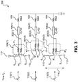
- Figures 3 and 4 are provided. Common elements between Figures 1 , 2A , 2B , 3 , and 4 are shown therein with common element numbers and will not be re-described herein.
- Figure 3 is a schematic diagram of an exemplary three-phase transmitter 300 configured to shift the rightmost crossing 206 leftward to reduce the signal skew 202.
- the three-phase transmitter 300 comprises a first signal branch 302(1), a second signal branch 302(2), and a third signal branch 302(3).
- the first signal branch 302(1), the second signal branch 302(2), and the third signal branch 302(3) include the respective branch impedances 104(1)-104(3) and respective driving impedances 304(1)-304(3).
- Each of the respective driving impedances 304(1)-304(3) includes a first resistor (R' 1 ) and a second resistor (R' 2 ) disposed in a parallel arrangement.
- the three-phase transmitter 300 receives the first branch signal 116(1), the second branch signal 116(2), and the third branch signal 116(3).
- the first branch signal 116(1) causes the first signal branch 302(1) to transition from being coupled to the upper mode voltage 110 to being coupled to the lower mode voltage 112.
- the switch Su of the first signal branch 302(1) is open and the switch S L of the first signal branch 302(1) is closed.
- the respective driving impedance 304(1) equals the R' 2 .
- the second branch signal 116(2) causes the second signal branch 302(2) to transition from being coupled to the common mode voltage 114 to being coupled to the upper mode voltage 110.
- the switch S L of the second signal branch 302(2) is open and the switch Su of the second signal branch 302(2) is closed.
- the second signal branch 302(2) transitions out of the common mode and the respective driving impedance 304(2) equals the R' 1 .
- the third branch signal 116(3) causes the third signal branch 302(3) to transition from being coupled to the lower mode voltage 112 to being coupled to the common mode voltage 114. Accordingly, both the switch S U and the switch S L of the third signal branch 302(3) are closed. In this regard, the third branch signal 116(3) causes the third signal branch 302(3) to transition into the common mode and function as the common mode branch. Since the R' 1 and the R' 2 are disposed in parallel arrangement, the respective driving impedance 304(3) equals an average of the resistance of the R' 1 and the resistance of the R' 2 ((R' 1 + R' 2 ) / 2).
- the resistances of the R' 1 and R' 2 are selected to ensure that the respective driving impedance 304(3) is less than the respective branch impedance 104(3).
- the R' 1 and the R' 2 may be selected to provide the respective driving impedance 304(3) as one-half of the respective branch impedance 104(3).
- the R' 1 and the R' 2 may each have 50 ⁇ resistance, thus configuring the respective driving impedance 304(3) to 25 ⁇ .
- RC resistor-capacitor
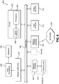
- Figure 4 is a schematic diagram of an exemplary three-phase communication circuit 400 comprising a pattern detector 402 configured to shift the leftmost crossing 204 rightward to reduce the signal skew 202.
- the three-phase communication circuit 400 comprises the three-phase transmitter 300 of Figure 3 .
- the three-phase transmitter 300 is configure to receive the first branch signal 116(1), the second branch signal 116(2), and the third branch signal 116(3) from a pre-driver circuit 404.
- the pre-driver circuit 404 generates the first branch signal 116(1), the second branch signal 116(2), and the third branch signal 116(3) based on a plurality of input streams 406(1)-406(N) received from an encoder 408.
- the encoder 408 generates the plurality of input streams 406(1)-406(N) based on a plurality of serialized data streams 410(1)-410(N) received from a plurality of serializers 412(1)-412(N), respectively.
- each of the plurality of serializers 412(1)-412(N) is a seven-to-one (7-1) serializer.
- the first signal branch 302(1), the second signal branch 302(2), and the third signal branch 302(3) are coupled to the upper mode voltage 110, the common mode voltage 114, and the lower mode voltage 112, respectively.
- the second signal branch 302(2) is in the common mode and functions as the common mode branch (the present common mode branch) at the time T X .
- the first branch signal 116(1), the second branch signal 116(2), and the third branch signal 116(3) respectively cause the first signal branch 302(1), the second signal branch 302(2), and the third signal branch 302(3) to be coupled to the lower mode voltage 112, the upper mode voltage 110, and the common mode voltage 114.
- the third signal branch 302(3) is in the common mode and functions as the common mode branch (the future common mode branch) at the time T Y .
- the present common mode branch which is the second signal branch 302(2)
- the future common mode branch which is the third signal branch 302(3)
- the pre-driver circuit 404 is configured to generate a first pattern signal 414(1), a second pattern signal 414(2), and a third pattern signal 414(3) that correspond with the first signal branch 302(1), the second signal branch 302(2), and the third signal branch 302(3), respectively.
- Each of the first pattern signal 414(1), the second pattern signal 414(2), and the third pattern signal 414(3) indicates a respective present voltage (not shown) and a respective future voltage (not shown) of a corresponding signal branch among the first signal branch 302(1), the second signal branch 302(2), and the third signal branch 302(3).
- the first pattern signal 414(1) indicates the respective present voltage and the respective future voltage of the first signal branch 302(1) at the time T X and the time T Y , respectively.
- the second pattern signal 414(2) indicates the respective present voltage and the respective future voltage of the second signal branch 302(2) at the time T X and the time T Y , respectively.
- the third pattern signal 414(3) indicates the respective present voltage and the respective future voltage of the third signal branch 302(3) at the time T X and the time T Y , respectively.
- the pattern detector 402 examines the first pattern signal 414(1), the second pattern signal 414(2), and the third pattern signal 414(3) to determine the present common mode branch among the first signal branch 302(1), the second signal branch 302(2), and the third signal branch 302(3).
- a signal branch among the first signal branch 302(1), the second signal branch 302(2), and the third signal branch 302(3) can be deemed as the present common mode branch if the respective present voltage of the signal branch equals the common mode voltage 114.
- the second signal branch 302(2) is the present common mode branch if the respective present voltage indicated by the second pattern signal 414(2) equals the common mode voltage 114.
- the pattern detector 402 is able to further determine the respective future voltage of the present common mode branch based on the respective future voltage indicated by the respective pattern signal. For example, if the second signal branch 302(2) is the present common mode branch, the pattern detector 402 is able to determine the future voltage of the second signal branch 302(2) based on the second pattern signal 414(2).
- the pattern detector 402 couples a current source 416 to the present common mode branch if the present common mode branch is transitioning to the respective future voltage that is lower than the common mode voltage 114.
- the pattern detector 402 couples a current sink 418 to the present common mode branch if the present common mode branch is transitioning to the respective future voltage that is higher than the common mode voltage 114.
- the current source 416 and the current sink 418 may be provided in a current digital-to-analog converter (DAC) circuit 420.
- DAC digital-to-analog converter
- the current source 416 and the current sink 418 may be integrated with the pattern detector 402.
- the pre-driver circuit 404 is configured to maintain synchronization between the first branch signal 116(1), the second branch signal 116(2), the third branch signal 116(3), the source-current signal 422, and the sink-current signal 424.
- the current source 416 or the current sink 418 can be coupled to the present common mode branch when the present common mode branch transitions out of the common mode at the time T Y .
- Figure 5A is an exemplary plot 500 illustrating one aspect of signal skew reduction provided by the three-phase transmitter 300 of Figure 3 and the three-phase communication circuit 400 of Figure 4 .
- Elements of Figure 2A are referenced in connection with Figure 5A and will not be re-described herein.
- the three-phase transmitter 300 is configured to expedite the RC setup in the three-phase transmitter 300.
- the expedited RC setup in the three-phase transmitter 300 helps move an original transition curve 502 to a new transition curve 504.
- the expedited RC setup makes the new transition curve 504 steeper than the original transition curve 502, thus shifting the rightmost crossing 206 leftward to the new rightmost crossing 206'.
- the pattern detector 402 couples the current sink 418 to the present common mode branch if the present common mode branch is transitioning to the respective future voltage that is higher than the common mode voltage 114.
- the second signal branch 302(2) which is the present common mode branch
- a previous transition curve 506 is moved to a present transition curve 508 by coupling the current sink 418 to the second signal branch 302(2).
- the leftmost crossing 204 is shifted rightward to the new leftmost crossing 204' as the present transition curve 508 becomes shallower than the previous transition curve 506.
- Figure 5B is an exemplary plot 510 illustrating another aspect of the signal skew reduction provided by the three-phase transmitter 300 of Figure 3 and the three-phase communication circuit 400 of Figure 4 .
- the pattern detector 402 couples the current source 416 to the present common mode branch if the present common mode branch is transitioning to the respective future voltage that is lower than the common mode voltage 114.
- the third signal branch 302(3) which is the present common mode branch
- the previous transition curve 506 is moved to the present transition curve 508 by coupling the current source 416 to the third signal branch 302(3).
- the leftmost crossing 204 is shifted rightward to the new leftmost crossing 204' as the present transition curve 508 becomes shallower than the previous transition curve 506.
- the three-phase transmitter 300 is configured to expedite the RC setup in the three-phase transmitter 300.
- the expedited RC setup helps move the original transition curve 502 to the new transition curve 504.
- the expedited RC setup makes the new transition curve 504 steeper than the original transition curve 502, thus shifting the rightmost crossing 206 leftward to the new rightmost crossing 206'.
- FIG. 6 is a flowchart illustrating an exemplary skew control process 600 employed by the three-phase transmitter 300 of Figure 3 to shift the rightmost crossing 206 leftward.
- the three-phase transmitter 300 identifies a signal branch among the first signal branch 302(1), the second signal branch 302(2), and the third signal branch 302(3), wherein the signal branch is selected to function as the common mode branch by being coupled to the common mode voltage 114 (block 602). Once the common mode branch is identified, the three-phase transmitter 300 configures the respective driving impedance 304(1)-304(3) of the selected signal branch to be less than the respective branch impedance 104(1)-104(3) of the selected signal branch (block 604).
- Figure 7 is a flowchart illustrating another exemplary skew control process 700 employed by the three-phase communication circuit 400 of Figure 4 to shift the leftmost crossing 204 rightward.
- the pattern detector 402 receives the first pattern signal 414(1), the second pattern signal 414(2), and the third pattern signal 414(3) indicating the respective present voltage and the respective future voltage of the first signal branch 302(1), the second signal branch 302(2), and the third signal branch 302(3), respectively (block 702).
- the pattern detector 402 then identifies the present common mode branch among the first signal branch 302(1), the second signal branch 302(2), and the third signal branch 302(3) based on the first pattern signal 414(1), the second pattern signal 414(2), and the third pattern signal 414(3), wherein the respective present voltage of the present common mode branch equals the common mode voltage 114 (block 704).
- the pattern detector 402 compares the respective future voltage of the present common mode branch with the common mode voltage 114 (block 706). If the respective future voltage of the present common mode branch is lower than the common mode voltage 114, the pattern detector 402 is configured to couple the current source 416 to the present common mode branch (block 708).
- the pattern detector 402 is configured to couple the current sink 418 to the present common mode branch (block 710).
- the skew control process 700 ends if the respective future voltage of the present common mode branch equals the common mode voltage 114 (block 712).
- the skew control for three-phase communication may be provided in or integrated into any processor-based device.
- Examples include a set top box, an entertainment unit, a navigation device, a communications device, a fixed location data unit, a mobile location data unit, a mobile phone, a cellular phone, a computer, a portable computer, a desktop computer, a personal digital assistant (PDA), a monitor, a computer monitor, a television, a tuner, a radio, a satellite radio, a music player, a digital music player, a portable music player, a digital video player, a video player, a digital video disc (DVD) player, and a portable digital video player.
- PDA personal digital assistant
- FIG. 8 illustrates an example of a processor-based system 800 that can employ the three-phase transmitter 300 of Figure 3 and the three-phase communication circuit 400 of Figure 4 .
- the processor-based system 800 includes one or more central processing units (CPUs) 802, each including one or more processors 804.
- the CPU(s) 802 may have cache memory 806 coupled to the processor(s) 804 for rapid access to temporarily stored data.
- the CPU(s) 802 is coupled to a system bus 808.
- the CPU(s) 802 communicates with these other devices by exchanging address, control, and data information over the system bus 808.
- multiple system buses 808 could be provided, wherein each system bus 808 constitutes a different fabric.
- Other master and slave devices can be connected to the system bus 808. As illustrated in Figure 8 , these devices can include a memory system 810, one or more input devices 812, one or more output devices 814, one or more network interface devices 816, and one or more display controllers 818, as examples.
- the three-phase transmitter 300 of Figure 3 and the three-phase communication circuit 400 of Figure 4 can also be connected to the system bus 808.
- the input device(s) 812 can include any type of input device, including, but not limited to, input keys, switches, voice processors, etc.
- the output device(s) 814 can include any type of output device, including, but not limited to, audio, video, other visual indicators, etc.
- the network interface device(s) 816 can be any device configured to allow exchange of data to and from a network 820.
- the network 820 can be any type of network, including, but not limited to, a wired or wireless network, a private or public network, a local area network (LAN), a wireless local area network (WLAN), a wide area network (WAN), a BLUETOOTHTM network, or the Internet.
- the network interface device(s) 816 can be configured to support any type of communications protocol desired.
- the memory system 810 can include one or more memory units 822(0-N) and a memory controller 824.
- the CPU(s) 802 may also be configured to access the display controller(s) 818 over the system bus 808 to control information sent to one or more displays 826.
- the display controller(s) 818 sends information to the display(s) 826 to be displayed via one or more video processors 828, which process the information to be displayed into a format suitable for the display(s) 826.
- the display(s) 826 can include any type of display, including, but not limited to, a cathode ray tube (CRT), a liquid crystal display (LCD), a plasma display, a light emitting diode (LED) display, etc.
- the three-phase communication circuit 400 of Figure 4 may also be provided in a digital camera 900 as illustrated by the exemplary schematic diagram of Figure 9 .
- DSP Digital Signal Processor
- ASIC Application Specific Integrated Circuit
- FPGA Field Programmable Gate Array
- a processor may be a microprocessor, but in the alternative, the processor may be any conventional processor, controller, microcontroller, or state machine.
- a processor may also be implemented as a combination of computing devices (e.g., a combination of a DSP and a microprocessor, a plurality of microprocessors, one or more microprocessors in conjunction with a DSP core, or any other such configuration).
- RAM Random Access Memory
- ROM Read Only Memory
- EPROM Electrically Programmable ROM
- EEPROM Electrically Erasable Programmable ROM
- registers a hard disk, a removable disk, a CD-ROM, or any other form of computer readable medium known in the art.
- An exemplary storage medium is coupled to the processor such that the processor can read information from, and write information to, the storage medium.
- the storage medium may be integral to the processor.
- the processor and the storage medium may reside in an ASIC.
- the ASIC may reside in a remote station.
- the processor and the storage medium may reside as discrete components in a remote station, base station, or server.
Landscapes
- Engineering & Computer Science (AREA)
- Computer Networks & Wireless Communication (AREA)
- Signal Processing (AREA)
- Power Engineering (AREA)
- Dc Digital Transmission (AREA)
- Cable Transmission Systems, Equalization Of Radio And Reduction Of Echo (AREA)
Applications Claiming Priority (3)
| Application Number | Priority Date | Filing Date | Title |
|---|---|---|---|
| US201462016937P | 2014-06-25 | 2014-06-25 | |
| US14/722,271 US9401731B2 (en) | 2014-06-25 | 2015-05-27 | Skew control for three-phase communication |
| PCT/US2015/032898 WO2015199883A1 (en) | 2014-06-25 | 2015-05-28 | Skew control for three-phase communication |
Publications (2)
| Publication Number | Publication Date |
|---|---|
| EP3161969A1 EP3161969A1 (en) | 2017-05-03 |
| EP3161969B1 true EP3161969B1 (en) | 2021-06-23 |
Family
ID=54931648
Family Applications (1)
| Application Number | Title | Priority Date | Filing Date |
|---|---|---|---|
| EP15730899.0A Active EP3161969B1 (en) | 2014-06-25 | 2015-05-28 | Skew control for three-phase communication |
Country Status (6)
| Country | Link |
|---|---|
| US (1) | US9401731B2 (enExample) |
| EP (1) | EP3161969B1 (enExample) |
| JP (1) | JP6577495B2 (enExample) |
| CN (1) | CN106464300B (enExample) |
| ES (1) | ES2885683T3 (enExample) |
| WO (1) | WO2015199883A1 (enExample) |
Families Citing this family (1)
| Publication number | Priority date | Publication date | Assignee | Title |
|---|---|---|---|---|
| US9819523B2 (en) * | 2016-03-09 | 2017-11-14 | Qualcomm Incorporated | Intelligent equalization for a three-transmitter multi-phase system |
Family Cites Families (17)
| Publication number | Priority date | Publication date | Assignee | Title |
|---|---|---|---|---|
| US3660675A (en) * | 1970-05-05 | 1972-05-02 | Honeywell Inc | Transmission line series termination network for interconnecting high speed logic circuits |
| US6194924B1 (en) * | 1999-04-22 | 2001-02-27 | Agilent Technologies Inc. | Multi-function controlled impedance output driver |
| US6643787B1 (en) | 1999-10-19 | 2003-11-04 | Rambus Inc. | Bus system optimization |
| US6346832B1 (en) | 2000-05-22 | 2002-02-12 | Motorola, Inc. | Multi-channel signaling |
| US6552582B1 (en) * | 2001-09-27 | 2003-04-22 | Applied Micro Circuits Corporation | Source follower for low voltage differential signaling |
| JP2005051496A (ja) * | 2003-07-28 | 2005-02-24 | Kanji Otsuka | 信号伝送システム及び信号伝送線路 |
| KR100699828B1 (ko) * | 2004-10-11 | 2007-03-27 | 삼성전자주식회사 | 임피던스 교정 회로와 이를 포함하는 집적 회로 및 이를이용한 출력 드라이버의 임피던스 조절 방법 |
| JP4957100B2 (ja) * | 2005-11-25 | 2012-06-20 | セイコーエプソン株式会社 | 送信回路、データ転送制御装置及び電子機器 |
| US9711041B2 (en) | 2012-03-16 | 2017-07-18 | Qualcomm Incorporated | N-phase polarity data transfer |
| US8064535B2 (en) * | 2007-03-02 | 2011-11-22 | Qualcomm Incorporated | Three phase and polarity encoded serial interface |
| US7737747B2 (en) | 2007-08-31 | 2010-06-15 | Texas Instruments Incorporated | Scheme for controlling rise-fall times in signal transitions |
| US8848810B2 (en) * | 2008-03-05 | 2014-09-30 | Qualcomm Incorporated | Multiple transmitter system and method |
| US7928765B2 (en) * | 2009-03-30 | 2011-04-19 | Lsi Corporation | Tuning high-side and low-side CMOS data-paths in CML-to-CMOS signal converter |
| JP5498319B2 (ja) * | 2010-08-24 | 2014-05-21 | パナソニック株式会社 | 電流制御装置および通信システム |
| US8446168B2 (en) | 2010-12-14 | 2013-05-21 | Qualcomm, Incorporated | Pre-emphasis technique for on-chip voltage-driven single-ended-termination drivers |
| DE112012003384A5 (de) * | 2011-08-16 | 2014-07-10 | Silicon Line Gmbh | Schaltungsanordnung und Verfahren zum Übertragen von Signalen |
| US8536913B2 (en) | 2012-01-20 | 2013-09-17 | Qualcomm Incorporated | Transition time lock loop with reference on request |
-
2015
- 2015-05-27 US US14/722,271 patent/US9401731B2/en active Active
- 2015-05-28 JP JP2016573094A patent/JP6577495B2/ja active Active
- 2015-05-28 CN CN201580034037.9A patent/CN106464300B/zh active Active
- 2015-05-28 ES ES15730899T patent/ES2885683T3/es active Active
- 2015-05-28 WO PCT/US2015/032898 patent/WO2015199883A1/en not_active Ceased
- 2015-05-28 EP EP15730899.0A patent/EP3161969B1/en active Active
Non-Patent Citations (1)
| Title |
|---|
| None * |
Also Published As
| Publication number | Publication date |
|---|---|
| US9401731B2 (en) | 2016-07-26 |
| EP3161969A1 (en) | 2017-05-03 |
| JP6577495B2 (ja) | 2019-09-18 |
| US20150381218A1 (en) | 2015-12-31 |
| CN106464300A (zh) | 2017-02-22 |
| CN106464300B (zh) | 2019-06-14 |
| WO2015199883A1 (en) | 2015-12-30 |
| ES2885683T3 (es) | 2021-12-15 |
| JP2017527149A (ja) | 2017-09-14 |
Similar Documents
| Publication | Publication Date | Title |
|---|---|---|
| US9009379B1 (en) | Communicating with MIPI-compliant devices using non-MIPI interfaces | |
| JP7259904B2 (ja) | 送信装置、送信方法、および通信システム | |
| US20230140526A1 (en) | Transmission device, transmission method, and communication system | |
| TWI691168B (zh) | C-phy接收器均衡 | |
| US9934192B2 (en) | Peripheral component interconnect express (PCIe) hosts adapted to support remote PCIe endpoints | |
| CN111800355A (zh) | 传输器、成像系统以及通信系统 | |
| US20190044757A1 (en) | Transmission device, transmission method, and communication system | |
| EP3161969B1 (en) | Skew control for three-phase communication | |
| JP2016006937A (ja) | 送信装置および通信システム | |
| KR101680733B1 (ko) | 고속 동기식 직렬 인터페이스(hsi)를 위한 멀티-레인 고속 인터페이스들, 및 관련된 시스템들 및 방법들 | |
| US9721625B2 (en) | Time-constrained data copying between storage media | |
| CN103516605A (zh) | 并行i/o总线接收器接口及用于校准其接收器的方法 | |
| JPWO2016092968A1 (ja) | 送信装置、受信装置、および通信システム | |
| JP6631531B2 (ja) | 送信装置、送信方法、および通信システム | |
| US12125457B2 (en) | Display Port (DP) sink device having main Phy circuit with plurality of DP connectors and plurality of AUX Phy circuits coupled to subsidiary link circuit | |
| JP5367539B2 (ja) | インターフェース装置 | |
| CN102289423A (zh) | 共用电视机和电脑的usb接口的系统、方法及电视机 | |
| CN106797354A (zh) | 发射器和通信系统 |
Legal Events
| Date | Code | Title | Description |
|---|---|---|---|
| STAA | Information on the status of an ep patent application or granted ep patent |
Free format text: STATUS: THE INTERNATIONAL PUBLICATION HAS BEEN MADE |
|
| PUAI | Public reference made under article 153(3) epc to a published international application that has entered the european phase |
Free format text: ORIGINAL CODE: 0009012 |
|
| STAA | Information on the status of an ep patent application or granted ep patent |
Free format text: STATUS: REQUEST FOR EXAMINATION WAS MADE |
|
| 17P | Request for examination filed |
Effective date: 20161108 |
|
| AK | Designated contracting states |
Kind code of ref document: A1 Designated state(s): AL AT BE BG CH CY CZ DE DK EE ES FI FR GB GR HR HU IE IS IT LI LT LU LV MC MK MT NL NO PL PT RO RS SE SI SK SM TR |
|
| AX | Request for extension of the european patent |
Extension state: BA ME |
|
| DAV | Request for validation of the european patent (deleted) | ||
| DAX | Request for extension of the european patent (deleted) | ||
| STAA | Information on the status of an ep patent application or granted ep patent |
Free format text: STATUS: EXAMINATION IS IN PROGRESS |
|
| 17Q | First examination report despatched |
Effective date: 20200424 |
|
| GRAP | Despatch of communication of intention to grant a patent |
Free format text: ORIGINAL CODE: EPIDOSNIGR1 |
|
| STAA | Information on the status of an ep patent application or granted ep patent |
Free format text: STATUS: GRANT OF PATENT IS INTENDED |
|
| INTG | Intention to grant announced |
Effective date: 20201009 |
|
| GRAS | Grant fee paid |
Free format text: ORIGINAL CODE: EPIDOSNIGR3 |
|
| GRAJ | Information related to disapproval of communication of intention to grant by the applicant or resumption of examination proceedings by the epo deleted |
Free format text: ORIGINAL CODE: EPIDOSDIGR1 |
|
| GRAL | Information related to payment of fee for publishing/printing deleted |
Free format text: ORIGINAL CODE: EPIDOSDIGR3 |
|
| STAA | Information on the status of an ep patent application or granted ep patent |
Free format text: STATUS: EXAMINATION IS IN PROGRESS |
|
| GRAP | Despatch of communication of intention to grant a patent |
Free format text: ORIGINAL CODE: EPIDOSNIGR1 |
|
| STAA | Information on the status of an ep patent application or granted ep patent |
Free format text: STATUS: GRANT OF PATENT IS INTENDED |
|
| INTC | Intention to grant announced (deleted) | ||
| INTG | Intention to grant announced |
Effective date: 20210212 |
|
| GRAA | (expected) grant |
Free format text: ORIGINAL CODE: 0009210 |
|
| STAA | Information on the status of an ep patent application or granted ep patent |
Free format text: STATUS: THE PATENT HAS BEEN GRANTED |
|
| AK | Designated contracting states |
Kind code of ref document: B1 Designated state(s): AL AT BE BG CH CY CZ DE DK EE ES FI FR GB GR HR HU IE IS IT LI LT LU LV MC MK MT NL NO PL PT RO RS SE SI SK SM TR |
|
| REG | Reference to a national code |
Ref country code: GB Ref legal event code: FG4D |
|
| REG | Reference to a national code |
Ref country code: CH Ref legal event code: EP |
|
| REG | Reference to a national code |
Ref country code: AT Ref legal event code: REF Ref document number: 1405214 Country of ref document: AT Kind code of ref document: T Effective date: 20210715 Ref country code: DE Ref legal event code: R096 Ref document number: 602015070636 Country of ref document: DE |
|
| REG | Reference to a national code |
Ref country code: IE Ref legal event code: FG4D |
|
| REG | Reference to a national code |
Ref country code: SE Ref legal event code: TRGR |
|
| REG | Reference to a national code |
Ref country code: NL Ref legal event code: FP |
|
| REG | Reference to a national code |
Ref country code: LT Ref legal event code: MG9D |
|
| PG25 | Lapsed in a contracting state [announced via postgrant information from national office to epo] |
Ref country code: LT Free format text: LAPSE BECAUSE OF FAILURE TO SUBMIT A TRANSLATION OF THE DESCRIPTION OR TO PAY THE FEE WITHIN THE PRESCRIBED TIME-LIMIT Effective date: 20210623 Ref country code: FI Free format text: LAPSE BECAUSE OF FAILURE TO SUBMIT A TRANSLATION OF THE DESCRIPTION OR TO PAY THE FEE WITHIN THE PRESCRIBED TIME-LIMIT Effective date: 20210623 Ref country code: HR Free format text: LAPSE BECAUSE OF FAILURE TO SUBMIT A TRANSLATION OF THE DESCRIPTION OR TO PAY THE FEE WITHIN THE PRESCRIBED TIME-LIMIT Effective date: 20210623 Ref country code: BG Free format text: LAPSE BECAUSE OF FAILURE TO SUBMIT A TRANSLATION OF THE DESCRIPTION OR TO PAY THE FEE WITHIN THE PRESCRIBED TIME-LIMIT Effective date: 20210923 |
|
| REG | Reference to a national code |
Ref country code: NO Ref legal event code: T2 Effective date: 20210623 Ref country code: AT Ref legal event code: MK05 Ref document number: 1405214 Country of ref document: AT Kind code of ref document: T Effective date: 20210623 |
|
| PG25 | Lapsed in a contracting state [announced via postgrant information from national office to epo] |
Ref country code: LV Free format text: LAPSE BECAUSE OF FAILURE TO SUBMIT A TRANSLATION OF THE DESCRIPTION OR TO PAY THE FEE WITHIN THE PRESCRIBED TIME-LIMIT Effective date: 20210623 Ref country code: GR Free format text: LAPSE BECAUSE OF FAILURE TO SUBMIT A TRANSLATION OF THE DESCRIPTION OR TO PAY THE FEE WITHIN THE PRESCRIBED TIME-LIMIT Effective date: 20210924 Ref country code: RS Free format text: LAPSE BECAUSE OF FAILURE TO SUBMIT A TRANSLATION OF THE DESCRIPTION OR TO PAY THE FEE WITHIN THE PRESCRIBED TIME-LIMIT Effective date: 20210623 |
|
| REG | Reference to a national code |
Ref country code: ES Ref legal event code: FG2A Ref document number: 2885683 Country of ref document: ES Kind code of ref document: T3 Effective date: 20211215 |
|
| PG25 | Lapsed in a contracting state [announced via postgrant information from national office to epo] |
Ref country code: SM Free format text: LAPSE BECAUSE OF FAILURE TO SUBMIT A TRANSLATION OF THE DESCRIPTION OR TO PAY THE FEE WITHIN THE PRESCRIBED TIME-LIMIT Effective date: 20210623 Ref country code: SK Free format text: LAPSE BECAUSE OF FAILURE TO SUBMIT A TRANSLATION OF THE DESCRIPTION OR TO PAY THE FEE WITHIN THE PRESCRIBED TIME-LIMIT Effective date: 20210623 Ref country code: CZ Free format text: LAPSE BECAUSE OF FAILURE TO SUBMIT A TRANSLATION OF THE DESCRIPTION OR TO PAY THE FEE WITHIN THE PRESCRIBED TIME-LIMIT Effective date: 20210623 Ref country code: EE Free format text: LAPSE BECAUSE OF FAILURE TO SUBMIT A TRANSLATION OF THE DESCRIPTION OR TO PAY THE FEE WITHIN THE PRESCRIBED TIME-LIMIT Effective date: 20210623 Ref country code: RO Free format text: LAPSE BECAUSE OF FAILURE TO SUBMIT A TRANSLATION OF THE DESCRIPTION OR TO PAY THE FEE WITHIN THE PRESCRIBED TIME-LIMIT Effective date: 20210623 Ref country code: PT Free format text: LAPSE BECAUSE OF FAILURE TO SUBMIT A TRANSLATION OF THE DESCRIPTION OR TO PAY THE FEE WITHIN THE PRESCRIBED TIME-LIMIT Effective date: 20211025 Ref country code: AT Free format text: LAPSE BECAUSE OF FAILURE TO SUBMIT A TRANSLATION OF THE DESCRIPTION OR TO PAY THE FEE WITHIN THE PRESCRIBED TIME-LIMIT Effective date: 20210623 |
|
| PG25 | Lapsed in a contracting state [announced via postgrant information from national office to epo] |
Ref country code: PL Free format text: LAPSE BECAUSE OF FAILURE TO SUBMIT A TRANSLATION OF THE DESCRIPTION OR TO PAY THE FEE WITHIN THE PRESCRIBED TIME-LIMIT Effective date: 20210623 |
|
| REG | Reference to a national code |
Ref country code: DE Ref legal event code: R097 Ref document number: 602015070636 Country of ref document: DE |
|
| PG25 | Lapsed in a contracting state [announced via postgrant information from national office to epo] |
Ref country code: DK Free format text: LAPSE BECAUSE OF FAILURE TO SUBMIT A TRANSLATION OF THE DESCRIPTION OR TO PAY THE FEE WITHIN THE PRESCRIBED TIME-LIMIT Effective date: 20210623 |
|
| PLBE | No opposition filed within time limit |
Free format text: ORIGINAL CODE: 0009261 |
|
| STAA | Information on the status of an ep patent application or granted ep patent |
Free format text: STATUS: NO OPPOSITION FILED WITHIN TIME LIMIT |
|
| 26N | No opposition filed |
Effective date: 20220324 |
|
| PG25 | Lapsed in a contracting state [announced via postgrant information from national office to epo] |
Ref country code: AL Free format text: LAPSE BECAUSE OF FAILURE TO SUBMIT A TRANSLATION OF THE DESCRIPTION OR TO PAY THE FEE WITHIN THE PRESCRIBED TIME-LIMIT Effective date: 20210623 |
|
| PG25 | Lapsed in a contracting state [announced via postgrant information from national office to epo] |
Ref country code: IT Free format text: LAPSE BECAUSE OF FAILURE TO SUBMIT A TRANSLATION OF THE DESCRIPTION OR TO PAY THE FEE WITHIN THE PRESCRIBED TIME-LIMIT Effective date: 20210623 |
|
| REG | Reference to a national code |
Ref country code: BE Ref legal event code: MM Effective date: 20220531 |
|
| PG25 | Lapsed in a contracting state [announced via postgrant information from national office to epo] |
Ref country code: MC Free format text: LAPSE BECAUSE OF FAILURE TO SUBMIT A TRANSLATION OF THE DESCRIPTION OR TO PAY THE FEE WITHIN THE PRESCRIBED TIME-LIMIT Effective date: 20210623 Ref country code: LU Free format text: LAPSE BECAUSE OF NON-PAYMENT OF DUE FEES Effective date: 20220528 |
|
| REG | Reference to a national code |
Ref country code: FR Ref legal event code: PLFP Year of fee payment: 9 |
|
| PG25 | Lapsed in a contracting state [announced via postgrant information from national office to epo] |
Ref country code: IE Free format text: LAPSE BECAUSE OF NON-PAYMENT OF DUE FEES Effective date: 20220528 |
|
| PG25 | Lapsed in a contracting state [announced via postgrant information from national office to epo] |
Ref country code: BE Free format text: LAPSE BECAUSE OF NON-PAYMENT OF DUE FEES Effective date: 20220531 |
|
| PG25 | Lapsed in a contracting state [announced via postgrant information from national office to epo] |
Ref country code: HU Free format text: LAPSE BECAUSE OF FAILURE TO SUBMIT A TRANSLATION OF THE DESCRIPTION OR TO PAY THE FEE WITHIN THE PRESCRIBED TIME-LIMIT; INVALID AB INITIO Effective date: 20150528 |
|
| PG25 | Lapsed in a contracting state [announced via postgrant information from national office to epo] |
Ref country code: MK Free format text: LAPSE BECAUSE OF FAILURE TO SUBMIT A TRANSLATION OF THE DESCRIPTION OR TO PAY THE FEE WITHIN THE PRESCRIBED TIME-LIMIT Effective date: 20210623 Ref country code: CY Free format text: LAPSE BECAUSE OF FAILURE TO SUBMIT A TRANSLATION OF THE DESCRIPTION OR TO PAY THE FEE WITHIN THE PRESCRIBED TIME-LIMIT Effective date: 20210623 |
|
| PG25 | Lapsed in a contracting state [announced via postgrant information from national office to epo] |
Ref country code: TR Free format text: LAPSE BECAUSE OF FAILURE TO SUBMIT A TRANSLATION OF THE DESCRIPTION OR TO PAY THE FEE WITHIN THE PRESCRIBED TIME-LIMIT Effective date: 20210623 |
|
| PG25 | Lapsed in a contracting state [announced via postgrant information from national office to epo] |
Ref country code: MT Free format text: LAPSE BECAUSE OF FAILURE TO SUBMIT A TRANSLATION OF THE DESCRIPTION OR TO PAY THE FEE WITHIN THE PRESCRIBED TIME-LIMIT Effective date: 20210623 |
|
| PGFP | Annual fee paid to national office [announced via postgrant information from national office to epo] |
Ref country code: SE Payment date: 20250311 Year of fee payment: 11 |
|
| PGFP | Annual fee paid to national office [announced via postgrant information from national office to epo] |
Ref country code: NL Payment date: 20250421 Year of fee payment: 11 |
|
| PGFP | Annual fee paid to national office [announced via postgrant information from national office to epo] |
Ref country code: DE Payment date: 20250409 Year of fee payment: 11 |
|
| PGFP | Annual fee paid to national office [announced via postgrant information from national office to epo] |
Ref country code: GB Payment date: 20250410 Year of fee payment: 11 Ref country code: ES Payment date: 20250609 Year of fee payment: 11 |
|
| PGFP | Annual fee paid to national office [announced via postgrant information from national office to epo] |
Ref country code: NO Payment date: 20250425 Year of fee payment: 11 |
|
| PGFP | Annual fee paid to national office [announced via postgrant information from national office to epo] |
Ref country code: FR Payment date: 20250409 Year of fee payment: 11 |
|
| PGFP | Annual fee paid to national office [announced via postgrant information from national office to epo] |
Ref country code: CH Payment date: 20250601 Year of fee payment: 11 |