EP3142147B1 - Bildsensor und verfahren zur herstellung davon - Google Patents
Bildsensor und verfahren zur herstellung davon Download PDFInfo
- Publication number
- EP3142147B1 EP3142147B1 EP16185700.8A EP16185700A EP3142147B1 EP 3142147 B1 EP3142147 B1 EP 3142147B1 EP 16185700 A EP16185700 A EP 16185700A EP 3142147 B1 EP3142147 B1 EP 3142147B1
- Authority
- EP
- European Patent Office
- Prior art keywords
- slice
- semiconductor
- semiconductor slice
- image sensor
- pixel
- Prior art date
- Legal status (The legal status is an assumption and is not a legal conclusion. Google has not performed a legal analysis and makes no representation as to the accuracy of the status listed.)
- Active
Links
Images



Classifications
-
- H—ELECTRICITY
- H10—SEMICONDUCTOR DEVICES; ELECTRIC SOLID-STATE DEVICES NOT OTHERWISE PROVIDED FOR
- H10F—INORGANIC SEMICONDUCTOR DEVICES SENSITIVE TO INFRARED RADIATION, LIGHT, ELECTROMAGNETIC RADIATION OF SHORTER WAVELENGTH OR CORPUSCULAR RADIATION
- H10F39/00—Integrated devices, or assemblies of multiple devices, comprising at least one element covered by group H10F30/00, e.g. radiation detectors comprising photodiode arrays
- H10F39/80—Constructional details of image sensors
- H10F39/803—Pixels having integrated switching, control, storage or amplification elements
- H10F39/8033—Photosensitive area
-
- H—ELECTRICITY
- H10—SEMICONDUCTOR DEVICES; ELECTRIC SOLID-STATE DEVICES NOT OTHERWISE PROVIDED FOR
- H10F—INORGANIC SEMICONDUCTOR DEVICES SENSITIVE TO INFRARED RADIATION, LIGHT, ELECTROMAGNETIC RADIATION OF SHORTER WAVELENGTH OR CORPUSCULAR RADIATION
- H10F39/00—Integrated devices, or assemblies of multiple devices, comprising at least one element covered by group H10F30/00, e.g. radiation detectors comprising photodiode arrays
- H10F39/10—Integrated devices
- H10F39/12—Image sensors
- H10F39/18—Complementary metal-oxide-semiconductor [CMOS] image sensors; Photodiode array image sensors
-
- H—ELECTRICITY
- H10—SEMICONDUCTOR DEVICES; ELECTRIC SOLID-STATE DEVICES NOT OTHERWISE PROVIDED FOR
- H10F—INORGANIC SEMICONDUCTOR DEVICES SENSITIVE TO INFRARED RADIATION, LIGHT, ELECTROMAGNETIC RADIATION OF SHORTER WAVELENGTH OR CORPUSCULAR RADIATION
- H10F39/00—Integrated devices, or assemblies of multiple devices, comprising at least one element covered by group H10F30/00, e.g. radiation detectors comprising photodiode arrays
- H10F39/011—Manufacture or treatment of image sensors covered by group H10F39/12
- H10F39/014—Manufacture or treatment of image sensors covered by group H10F39/12 of CMOS image sensors
-
- H—ELECTRICITY
- H10—SEMICONDUCTOR DEVICES; ELECTRIC SOLID-STATE DEVICES NOT OTHERWISE PROVIDED FOR
- H10F—INORGANIC SEMICONDUCTOR DEVICES SENSITIVE TO INFRARED RADIATION, LIGHT, ELECTROMAGNETIC RADIATION OF SHORTER WAVELENGTH OR CORPUSCULAR RADIATION
- H10F39/00—Integrated devices, or assemblies of multiple devices, comprising at least one element covered by group H10F30/00, e.g. radiation detectors comprising photodiode arrays
- H10F39/011—Manufacture or treatment of image sensors covered by group H10F39/12
- H10F39/018—Manufacture or treatment of image sensors covered by group H10F39/12 of hybrid image sensors
-
- H—ELECTRICITY
- H10—SEMICONDUCTOR DEVICES; ELECTRIC SOLID-STATE DEVICES NOT OTHERWISE PROVIDED FOR
- H10F—INORGANIC SEMICONDUCTOR DEVICES SENSITIVE TO INFRARED RADIATION, LIGHT, ELECTROMAGNETIC RADIATION OF SHORTER WAVELENGTH OR CORPUSCULAR RADIATION
- H10F39/00—Integrated devices, or assemblies of multiple devices, comprising at least one element covered by group H10F30/00, e.g. radiation detectors comprising photodiode arrays
- H10F39/011—Manufacture or treatment of image sensors covered by group H10F39/12
- H10F39/026—Wafer-level processing
-
- H—ELECTRICITY
- H10—SEMICONDUCTOR DEVICES; ELECTRIC SOLID-STATE DEVICES NOT OTHERWISE PROVIDED FOR
- H10F—INORGANIC SEMICONDUCTOR DEVICES SENSITIVE TO INFRARED RADIATION, LIGHT, ELECTROMAGNETIC RADIATION OF SHORTER WAVELENGTH OR CORPUSCULAR RADIATION
- H10F39/00—Integrated devices, or assemblies of multiple devices, comprising at least one element covered by group H10F30/00, e.g. radiation detectors comprising photodiode arrays
- H10F39/10—Integrated devices
- H10F39/12—Image sensors
- H10F39/18—Complementary metal-oxide-semiconductor [CMOS] image sensors; Photodiode array image sensors
- H10F39/189—X-ray, gamma-ray or corpuscular radiation imagers
-
- H—ELECTRICITY
- H10—SEMICONDUCTOR DEVICES; ELECTRIC SOLID-STATE DEVICES NOT OTHERWISE PROVIDED FOR
- H10F—INORGANIC SEMICONDUCTOR DEVICES SENSITIVE TO INFRARED RADIATION, LIGHT, ELECTROMAGNETIC RADIATION OF SHORTER WAVELENGTH OR CORPUSCULAR RADIATION
- H10F39/00—Integrated devices, or assemblies of multiple devices, comprising at least one element covered by group H10F30/00, e.g. radiation detectors comprising photodiode arrays
- H10F39/10—Integrated devices
- H10F39/12—Image sensors
- H10F39/18—Complementary metal-oxide-semiconductor [CMOS] image sensors; Photodiode array image sensors
- H10F39/189—X-ray, gamma-ray or corpuscular radiation imagers
- H10F39/1898—Indirect radiation image sensors, e.g. using luminescent members
-
- H—ELECTRICITY
- H10—SEMICONDUCTOR DEVICES; ELECTRIC SOLID-STATE DEVICES NOT OTHERWISE PROVIDED FOR
- H10F—INORGANIC SEMICONDUCTOR DEVICES SENSITIVE TO INFRARED RADIATION, LIGHT, ELECTROMAGNETIC RADIATION OF SHORTER WAVELENGTH OR CORPUSCULAR RADIATION
- H10F39/00—Integrated devices, or assemblies of multiple devices, comprising at least one element covered by group H10F30/00, e.g. radiation detectors comprising photodiode arrays
- H10F39/10—Integrated devices
- H10F39/12—Image sensors
- H10F39/199—Back-illuminated image sensors
-
- H—ELECTRICITY
- H10—SEMICONDUCTOR DEVICES; ELECTRIC SOLID-STATE DEVICES NOT OTHERWISE PROVIDED FOR
- H10F—INORGANIC SEMICONDUCTOR DEVICES SENSITIVE TO INFRARED RADIATION, LIGHT, ELECTROMAGNETIC RADIATION OF SHORTER WAVELENGTH OR CORPUSCULAR RADIATION
- H10F39/00—Integrated devices, or assemblies of multiple devices, comprising at least one element covered by group H10F30/00, e.g. radiation detectors comprising photodiode arrays
- H10F39/80—Constructional details of image sensors
- H10F39/802—Geometry or disposition of elements in pixels, e.g. address-lines or gate electrodes
- H10F39/8023—Disposition of the elements in pixels, e.g. smaller elements in the centre of the imager compared to larger elements at the periphery
-
- H—ELECTRICITY
- H10—SEMICONDUCTOR DEVICES; ELECTRIC SOLID-STATE DEVICES NOT OTHERWISE PROVIDED FOR
- H10F—INORGANIC SEMICONDUCTOR DEVICES SENSITIVE TO INFRARED RADIATION, LIGHT, ELECTROMAGNETIC RADIATION OF SHORTER WAVELENGTH OR CORPUSCULAR RADIATION
- H10F39/00—Integrated devices, or assemblies of multiple devices, comprising at least one element covered by group H10F30/00, e.g. radiation detectors comprising photodiode arrays
- H10F39/80—Constructional details of image sensors
- H10F39/802—Geometry or disposition of elements in pixels, e.g. address-lines or gate electrodes
- H10F39/8027—Geometry of the photosensitive area
-
- H—ELECTRICITY
- H10—SEMICONDUCTOR DEVICES; ELECTRIC SOLID-STATE DEVICES NOT OTHERWISE PROVIDED FOR
- H10F—INORGANIC SEMICONDUCTOR DEVICES SENSITIVE TO INFRARED RADIATION, LIGHT, ELECTROMAGNETIC RADIATION OF SHORTER WAVELENGTH OR CORPUSCULAR RADIATION
- H10F39/00—Integrated devices, or assemblies of multiple devices, comprising at least one element covered by group H10F30/00, e.g. radiation detectors comprising photodiode arrays
- H10F39/80—Constructional details of image sensors
- H10F39/807—Pixel isolation structures
-
- H—ELECTRICITY
- H10—SEMICONDUCTOR DEVICES; ELECTRIC SOLID-STATE DEVICES NOT OTHERWISE PROVIDED FOR
- H10F—INORGANIC SEMICONDUCTOR DEVICES SENSITIVE TO INFRARED RADIATION, LIGHT, ELECTROMAGNETIC RADIATION OF SHORTER WAVELENGTH OR CORPUSCULAR RADIATION
- H10F39/00—Integrated devices, or assemblies of multiple devices, comprising at least one element covered by group H10F30/00, e.g. radiation detectors comprising photodiode arrays
- H10F39/80—Constructional details of image sensors
- H10F39/809—Constructional details of image sensors of hybrid image sensors
-
- H—ELECTRICITY
- H10—SEMICONDUCTOR DEVICES; ELECTRIC SOLID-STATE DEVICES NOT OTHERWISE PROVIDED FOR
- H10F—INORGANIC SEMICONDUCTOR DEVICES SENSITIVE TO INFRARED RADIATION, LIGHT, ELECTROMAGNETIC RADIATION OF SHORTER WAVELENGTH OR CORPUSCULAR RADIATION
- H10F39/00—Integrated devices, or assemblies of multiple devices, comprising at least one element covered by group H10F30/00, e.g. radiation detectors comprising photodiode arrays
- H10F39/80—Constructional details of image sensors
- H10F39/811—Interconnections
Definitions
- the present disclosure relates generally to image sensors and methods for manufacturing image sensors.
- Image sensors manufactured as image detectors typically are rectangular shaped and are formed over wafers (semiconductor material) that are round. Forming rectangular shaped image sensors over a round wafer does not fully utilize area of the wafer, resulting in wasted space. Image sensors components that are too large to be formed over portions of the round wafer are formed on a different wafer. Tiling different image sensors components formed over different wafers is both technically difficult and financially costly. Furthermore, pixel arrays on these image sensors are exposed to beams of radiation that that are circular shaped. Given that the pixel arrays are rectangular shaped, sections of the pixel arrays outside of an area exposed to a beam of radiation cannot be utilized.
- One proposal to decrease wasted space and to increase yield potential of the pixel arrays is to form a non-rectangular shaped image sensor that has dimensions approximate to an area exposed by the beam and to form non-rectangular shaped pixel arrays over the non-rectangular shaped image sensor.
- a non-rectangular shaped image sensor unlike a rectangular shaped image sensor, does not have uniform width.
- the non-rectangular shape of the pixel array causes some of the other components of the image sensor to come into contact with the pixel array, and renders pixels in contact with other components of the image sensor unusable.
- US2009/179141A1 discloses a large image sensor created by tiling a plurality of image sensor dies, wherein each of the image sensor dies includes a pixel array that extends to three edges of the die and control circuitry located along the fourth edge of the die. An insulating guard ring is located at the edges of the image sensor die.
- the disclosed embodiments provide non-rectangular shaped image sensors and methods to manufacture non-rectangular shaped image sensors that provide increased yield potential without a significant increase in production costs or manufacturing complexity.
- CMOS image sensor includes a plurality of semiconductor slices having a uniform width.
- the plurality of semiconductor slices are formed of different lengths and are arranged to form a semi-rectangular shape defining boundaries of the CMOS image sensor.
- Each of the plurality of semiconductor slices is disposed proximate to another semiconductor slice of the plurality of semiconductor slices.
- each semiconductor slice of the plurality of semiconductor slices has a slice edge defining a side of the semiconductor slice.
- Each semiconductor slice of the plurality of semiconductor slices includes a plurality of pixel arrays having an approximately uniform pixel pitch.
- Each semiconductor slice of the plurality of semiconductor slices also includes a guard ring having n type conductivity surrounding the plurality of pixel arrays.
- Each semiconductor slice of the plurality of semiconductor slices also includes a seal ring enclosing the semiconductor slice.
- Each semiconductor slice of the plurality of semiconductor slices further includes a column of row-driver circuitry. The column of row-driver circuitry is positioned proximate to the plurality of pixel arrays along a first side of the plurality of pixel arrays.
- the guard ring, the row-driver circuitry, the slice edge, the seal ring, a seal ring of another semiconductor slice disposed proximate to the semiconductor slice, a slice edge of the other semiconductor slice, and a guard ring of the other semiconductor slice have a combined width of less than or equal to one pixel pitch.
- an image sensor includes a plurality of semiconductor slices having a uniform width.
- the plurality of semiconductor slices are formed of different lengths and are arranged to form a semi-rectangular shape defining boundaries of the image sensor.
- Each of the plurality of semiconductor slices is disposed proximate to another semiconductor slice of the plurality of semiconductor slices.
- Each semiconductor slice of the plurality of semiconductor slices has a slice edge defining a side of the semiconductor slice.
- Each semiconductor slice of the plurality of semiconductor slices includes a plurality of pixel arrays having a uniform pixel pitch.
- Each semiconductor slice of the plurality of semiconductor slices also includes a seal ring enclosing the semiconductor slice.
- Each semiconductor slice of the plurality of semiconductor slices also includes a column of row-driver circuitry.
- a method for manufacturing an image sensor according to claim 11 includes forming a plurality of semiconductor slices having a uniform width. At least two of the plurality of semiconductor slices have different lengths, and each of the plurality of semiconductor slices has a slice edge defining a side of the semiconductor slice. The method further includes arranging the plurality of semiconductor slices to form a semi-rectangular shape defining boundaries of the image sensor, each of the plurality of semiconductor slices being disposed proximate to another semiconductor slice of the plurality of semiconductor slices. For each semiconductor slice of the plurality of semiconductor slices, the method further includes forming a plurality of pixel arrays over the semiconductor slice, the plurality of pixel arrays having an approximately uniform pixel pitch.
- the method further includes forming a seal ring around the semiconductor slice, the seal ring enclosing the semiconductor slice and the plurality of pixel arrays of the semiconductor slice, where each of the plurality of semiconductor slices has a different seal ring.
- Figure 1 illustrates an image sensor 100 in accordance with one example.
- the image sensor 100 has dimensions defined by boundaries 102.
- the image sensor 100 as illustrated in Figure 1 has circular dimensions.
- the image sensor 100 may be manufactured to form a variety of shapes, including rectangular shapes, and semi-rectangular shapes, which as used herein, includes any shape that is not rectangular.
- the image sensor 100 is fabricated on a mono-crystalline semiconductor substrate 103. Alternatively, the image sensor 100 may be fabricated on a polysilicon substrate or a substrate made of any other suitable semiconductor material. As illustrated in Figure 1 , components of the image sensor 100 are formed over different portions of the substrate 103 during photolithography.
- Image sensor 100 includes a first semiconductor slice 104, a second semiconductor slice 106, a third semiconductor slice 108, and a fourth semiconductor slice 110.
- the first, second, third, and fourth semiconductor slices 104, 106, 108, and 110 are formed over areas of the substrate 103 and include components configured to detect and measure electromagnetic radiation generated by one or more beams of electromagnetic radiation energy.
- each of the semiconductor slices 104, 106, 108, and 110 includes components that are configured to perform functions separate from the other semiconductor slices.
- Various components formed over each of the semiconductor slices 104, 106, 108, and 110 are discussed in greater detail in the paragraphs below.
- the first, second, third, and fourth semiconductor slices 104, 106, 108, and 110 have rectangular shapes and have an approximately uniform width. As used herein, an "approximately uniform width" is defined to include uniform width. Furthermore, the first, second, third, and fourth semiconductor slices 104, 106, 108, and 110 each has two sides at slice edges 152A and 152B, 154A and 154B, 156A and 156B, and 158A and 158B, respectively. In some examples, a slice edge defines a side of a semiconductor slice.
- the slice edge defines a transition area having a finite width along a side of the semiconductor slice between a seal ring that surrounds the semiconductor slice and a guard ring that is proximate to the slice edge. In other examples, the slice edge defines transition areas proximate to a different number of sides of the semiconductor slice.
- the image sensor 100 illustrated in Figure 1 includes four semiconductor slices 104, 106, 108, and 110 aligned proximate to each other to form a semi-rectangular area.
- a "semi-rectangular" shape is defined as any enclosed area that does not form a rectangular shape. Accordingly, a semi-rectangular shape includes ellipses.
- an "ellipse” is defined as a curve on a plane surrounding two focal points such that the sum of the distances to the two focal points is constant for every point on the curve.
- An ellipse is defined to include a circle, which is a special type of ellipse, where both foci are at the same point.
- the first semiconductor slice 104 includes pixel arrays 112, 114, and 116 formed over the first semiconductor slice 104.
- Each of the pixel arrays 112, 114, and 116 includes a plurality of individual pixels (not shown) arranged in rows and columns. Pixels are discussed in detail in the paragraphs below.
- Each of the pixel arrays 112, 114, and 116 is configured to receive electromagnetic radiation information and to output a corresponding signal. While the first semiconductor slice 104 illustrated in FIG. 1 includes three pixel arrays 112, 114, and 116, in other examples, the pixel arrays 112, 114, and 116 combine to form one pixel array. In a preferred example, the pixel arrays 112, 114, and 116 are manufactured using CMOS technology.
- the pixel arrays 112, 114, and 116 may be manufactured using CCD or other similar technologies.
- the pixel arrays 112, 114, and 116 are covered by a layer of a scintillator material.
- the scintillator material converts incoming x-ray photons into a form of visible light (e.g., a green light).
- the pixel arrays 112, 114, and 116 convert the green light into electrical signals corresponding to the incoming x-ray photons.
- electromagnetic radiation signals from a wide frequency range including, but not limited to, gamma ray radiation, ultraviolet radiation, visible light radiation, and infrared radiation can be converted by an optional conversion layer into a form of visible light and further converted by the pixel arrays 112, 114, and 116 to electrical signals, or directly converted by the pixel arrays 112, 114, and 116 to electrical signals.
- the semiconductor slice 104 includes a guard ring (not shown) formed around the pixel arrays 112, 114, and 116 to insulate the pixel arrays 112, 114, and 116 from noise generated by other components formed or present over the substrate 103. Guard rings are illustrated and are discussed in greater detail in the paragraphs below.
- the image sensor 100 illustrated in Figure 1 also includes pixel arrays 118, 120, 122, 124, and 126, formed over the second semiconductor slice 106. Furthermore, the image sensor 100 also includes pixel arrays 128, 130, 132, 134, and 136, formed over the third semiconductor slice 108. Furthermore, the image sensor 100 also includes pixel arrays 138, 140, and 142, formed over the fourth semiconductor slice 110. Together, the pixel arrays 112, 114, 116, 118, 120, 122, 124, 126, 128, 130, 132, 134, 136, 138, 140, and 142 are arranged to form a semi-rectangular area that surrounds an area of electromagnetic radiation exposure 190. According to another example, a different number of pixel arrays are formed over their respective semiconductor slices to form an area covering an area of electromagnetic radiation exposure having dimensions different from the dimensions of the area of electromagnetic radiation exposure 190.
- the pixel arrays 112, 114, 116, 118, 120, 122, 124, 126, 128, 130, 132, 134, 136, 138, 140, and 142 are arranged to form a shape similar to the area of electromagnetic radiation exposure 190.
- the pixel arrays 112, 114, 116, 118, 120, 122, 124, 126, 128, 130, 132, 134, 136, 138, 140, and 142 are arranged to form an area identical to, approximately the same as, or slightly greater than the area of electromagnetic radiation exposure 190 in order to ensure substantial coverage of the area of electromagnetic radiation exposure and to maximize the yield potential of the pixel arrays 112, 114, 116, 118, 120, 122, 124, 126, 128, 130, 132, 134, 136, 138, 140, and 142.
- the pixel arrays 112, 114, 116, 118, 120, 122, 124, 126, 128, 130, 132, 134, 136, 138, 140, and 142 can be arranged to form an area slightly smaller than the area of electromagnetic radiation exposure 190 to reduce the required surface area of the pixel array and yet maintain substantial coverage of the area of radiation exposure.
- the slices of pixel arrays are rectangular shaped and selected to be of different heights to best approximate the general shape of an arcuate area of electromagnetic radiation, the height and arrangement of such slices may be varied in different examples.
- each pixel array of the pixel arrays 112, 114, 116, 118, 120, 122, 124, 126, 128, 130, 132, 134, 136, 138, 140, and 142 is partially or completely within the area electromagnetic radiation exposure 190.
- the first semiconductor slice 104 also includes control and readout circuitry 144 formed over the first semiconductor slice 104.
- the readout circuitry 144 includes circuitry such as analog-to-digital conversion (ADC) circuitry.
- ADC analog-to-digital conversion
- the control and readout circuitry 144 is configured to control operations performed by the pixel arrays 112, 114, and 116 and row-driver circuitry formed over the first semiconductor slice 104 (not shown).
- the control and readout circuitry 144 may also be configured to convert analog signals of electromagnetic radiation received at the pixel arrays 112, 114, and 116 into a digital representation.
- the second semiconductor slice 106 includes control and readout circuitry 146 formed over the second semiconductor slice 106.
- the control and readout circuitry 146 is configured to control operations performed by the pixel arrays 118, 120, 122, 124, and 126 and row-driver circuitry formed over the second semiconductor slice 106 (not shown).
- the third semiconductor slice 108 includes control and readout circuitry 148 formed over the third semiconductor slice 108.
- the control and readout circuitry 148 is configured to control operations performed by the pixel arrays 128, 130, 132, 134, and 136 and row-driver circuitry formed over the third semiconductor slice 108 (not shown).
- the fourth semiconductor slice 110 includes control and readout circuitry 150 formed over the fourth semiconductor slice 110.
- the control and readout circuitry 150 is configured to control operations performed by the pixel arrays 138, 140, and 142 and row-driver circuitry formed over the fourth semiconductor slice 110 (not shown).
- control and readout circuitry 144 is configured to control pixel arrays 112, 114, and 116 independent from control and readout circuitries 146, 148, and 150.
- control and readout circuitry 144 is configured to convert analog signals of electromagnetic radiation received at the pixel arrays 112, 114, and/or 116 into digital representations of the received signals independent from control and readout circuitries 146, 148, 150.
- control and readout circuitries 146, 148, and 150 are configured to control pixel arrays formed over semiconductor slice 106, 108, or 110, respectively, independent from other control and readout circuitries.
- the image sensor 100 can operate with greater efficiency. Furthermore, if the control and readout circuitry formed over a semiconductor slice malfunctions, the malfunction is local to the semiconductor slice and does not prevent other control and readout circuitries formed over other semiconductor slices from receiving and converting analog signals of electromagnetic radiation received at pixel arrays formed over the other semiconductor slices.
- control and readout circuitry 144 is disposed proximate to the pixel array 116
- the control and readout circuitry 146 is disposed proximate to the pixel array 126
- the control and readout circuitry 148 is disposed proximate to pixel array 136
- the control and readout circuitry 150 is disposed proximate to the pixel array 142.
- control and readout circuitries 144, 146, 148, and/or 150 are disposed adjacent to multiple pixel arrays.
- the control and readout circuitries 144, 146, 148, and/or 150 are disposed at a different location on their respective semiconductor slice.
- control and readout circuitries 144, 146, 148, and/or 150 each includes two or more components that are disposed at different locations on their respective semiconductor slices. Additional control and readout circuitry (not shown) may also be formed over each of the semiconductor slices 104, 106, 108, and 110 to facilitate conversion of analog signals of electromagnetic radiation received at pixel arrays formed over the respective semiconductor slice into digital signals and to serve as back up in case one of the control and readout circuitries 144, 146, 148, and 150 malfunctions.
- the semiconductor devices formed on the first semiconductor slice 104 are enclosed by a seal ring 160.
- the seal ring 160 is a trench that extends around the periphery of the first semiconductor slice 104.
- the seal ring 160 may be a trench that extends around the periphery of the first semiconductor slice 104 but is filled with a material different than the substrate material which is typically silicon or other suitable materials.
- the seal ring 160 includes metal layers, dielectric layers, and via. In such example, a metal layer of the seal ring 160 is electrically connected to a p type substrate. The seal ring 160 is also electrically connected and/or coupled to a ground connection.
- the seal ring 160 is generally rectangular in shape and includes two sets of opposed generally parallel sides and adjacent sides that are generally orthogonal to each other. However, in one example, the seal ring 160 may have arcuate or polygonal corner junctions to prevent stress and charge concentration that may damage the first semiconductor slice 104.
- the seal ring 160 protects the semiconductor devices formed on the first semiconductor slice 104 from stress energy of other slices or electrical components external to the first semiconductor slice 104. Stress energy in components external to the semiconductor slice 104 could propagate to and destroy the semiconductor devices on the first semiconductor slice 104 on the semiconductor chip if not for the presence of the seal ring 160.
- the seal ring 160 also protects the components formed over the first semiconductor slice 104 from abutting against other components formed over other semiconductor slices.
- seal ring 160 also maintains structural integrity of the first semiconductor slice 104 and components formed over the first semiconductor slice 104 during different photolithography procedures.
- seal rings 162, 164, and 166 also provide similar protection for components formed on the second, third, and fourth semiconductor slices 106, 108, and 110, respectively.
- Additional circuitries such as, but not limited to row-driver circuitry are formed over the first, second, third, and fourth semiconductor slices 104, 106, 108, and 110.
- additional components such as printed circuit board (PCB), scintillator materials, etc., may also be formed over and/or disposed proximate to the substrate 103. Details of these components are further discussed in the paragraphs below and are illustrated by subsequent figures.
- PCB printed circuit board
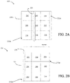
- FIG. 2A illustrates a semiconductor slice containing a pixel array 201A and row-driver circuitry 220 in accordance with one example.
- the pixel array 201A is a 3x3 grid and includes pixels 202, 204, 206, 208, 210, 212, 214, 216, and 218.
- the pixel array 201A has a pixel pitch defined by an approximate width of a pixel in the pixel array 201A.
- the pixel array 201A is formed over semiconductor slice 200, which has two sides defined by slice edges 222A and 222B.
- the row-driver circuitry 220 is configured to deliver voltage to the pixels 202, 204, 206, 208, 210, 212, 214, 216, and 218 to control the accumulation, transfer, and resetting of signals accumulated in each pixel.
- the row-driver circuitry 220 may also be configured to control the transfer of signals received at the pixels 202, 204, 206, 208, 210, 212, 214, 216, and 218 of the pixel array 201A to a control and readout circuitry (not shown). As illustrated in Figure 2A , the row-driver circuitry 220 is disposed proximate to pixels 204, 210, and 216.
- the presence of the row-driver circuitry 220 proximate to the pixels 204, 210, and 216 reduces the surface area of the pixels, and thereby reduces the sensitivity of the pixels 204, 210, and 216 to electromagnetic radiation. As such, a column of pixels proximate to the row-driver circuitry 220 is considered a dead column.
- Figure 2B illustrates a semiconductor slice containing a pixel array 251 and row-driver circuitry 270 in accordance with another example.
- the pixel array 251 is also a 3x3 grid and includes pixels 252, 254, 256, 258, 260, 262, 264, 266, and 268.
- the pixel array 251 is formed over semiconductor slice 250, which has two sides defined by slice edges 272A and 272B.
- the row-driver circuitry 270 is disposed along a side of the pixel array 251 and is disposed proximate to pixels 252, 258, and 264.
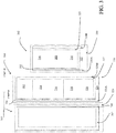
- Figure 3 illustrates three semiconductor slices 302, 304 and 305 disposed proximate to each other in accordance with one embodiment.
- a first semiconductor slice 302 has two sides defined by slice edges 326A and 326B and is enclosed by a seal ring 330.
- slice edges 326A and 326B define two sides of the semiconductor slice 302.
- Pixel arrays 306, 308, and 310 are formed over first semiconductor slice 302.
- Control and readout circuitry 322 and row-driver circuitry 332 are disposed over the first semiconductor slice 302.
- a guard ring 325 is formed around the pixel arrays 306, 308, and 310 of the first semiconductor slice 302.
- the guard ring 325 is doped to have a n type electrical conductivity. In other embodiments, the guard ring 325 is doped to have a p type electrical conductivity.
- the guard ring 325 extends down to a subsurface of the substrate of the three semiconductor slices 302, 304, and 305, and is formed to insulate the pixel arrays 306, 308, and 310 from noise generated by other components (e.g., the control and readout circuitry 322, the row-driver circuitry 332, etc.,) formed or present over the substrate.
- a single guard ring 325 is formed around the pixel arrays 306, 308, and 310. Additional guard rings may also be formed around one or more pixels of the pixel arrays 306, 308, and 310 to insulate the one or more pixels from noise generated by other pixels of the pixel arrays 306, 308, and 310, and from noise generated by other components formed over the substrate. In other embodiments, a separate guard ring is formed around each pixel of the pixel arrays 306, 308, and 310 to further insulate the respective pixel from noise generated by other pixels and/or other components formed over the substrate. In such embodiments, the single guard ring 325 may not be formed around the pixel arrays 306, 308, and 310. In other embodiments, a guard ring is not formed around any of the pixel arrays 306, 308, 310, 312, 314, 316, 318, or 320.
- a second semiconductor slice 304 has two sides defined by slice edges 328A and 328B and is enclosed by a seal ring 338.
- Figure 3 also illustrates a third semiconductor slice 305 disposed proximate to the second semiconductor slice 304.
- the third semiconductor slice 305 has a side defined by a slice edge 340 and is enclosed by a seal ring 336.
- Seal rings 330, 336, and 338 do not include any component configured to receive electromagnetic radiation information. As such, areas of the substrate covered by the seal rings 330, 336, and 338 are not configured to receive electromagnetic radiation information and are considered dead space.
- Pixel arrays 312, 314, 316, 318, and 320 are formed over the second semiconductor slice 304.
- a guard ring 337 is formed around the pixel arrays 312, 314, 316, 318, and 320 of the second semiconductor 304 to insulate the pixel arrays 312, 314, 316, 318, and 320 from noise generated by other components that are formed on the substrate.
- the second semiconductor slice 304 also includes control and readout circuitry 324 and row-driver circuitry 334 disposed over the second semiconductor slice 304. Similar to the configuration illustrated in FIG.
- row-driver circuitries 332 and 334 are disposed on a side of pixel arrays 306, 308, 310, 312, 314, 316, 318, and 320 and are proximate to pixels located on the edge of the pixel arrays 306, 308, 310, 312, 314, 316, 318, and 320.
- the guard ring 325 of the first semiconductor slice 302, the row-driver circuitry 332 of the first semiconductor slice 302, the slice edge 326A of the first semiconductor slice 302, the seal ring 330 of the first semiconductor slice 302, the seal ring 338 of the second semiconductor slice 304, the slice edge 328B of the second semiconductor slice 304, and the guard ring 337 of the second semiconductor slice 304 are fabricated to have a combined width of less than one pixel pitch.
- the combined width of row-driver circuitry 332, the guard rings 325 and 337, the slice edges 326A and 328B, and the seal rings 330 and 338 are fabricated to have a width of up to two pixel pitches.
- the width of the row-driver circuitry 332, the guard rings 325 and 337, the slice edges 326A and 328B, and/or the seal rings 330 and 338 are increased in order to accommodate various fabrication implementations and semiconductor device requirements, such as, but not limited to, noise tolerance level of the components of the pixel arrays formed on the substrate, the amount of stress the substrate is subject to during the fabrication process, the type of semiconductor devices used to form the row-driver circuitries, the number of semiconductor devices used to form the row-driver circuitries, and dimensions of the semiconductor slices formed over the substrate.
- the guard ring 325 has wide trenches to insulate the pixel arrays 306, 308, and 310.
- multiple stitching operations are performed during the fabrication process.
- seal rings 330 and 338 have wide trenches to protect components formed over the semiconductor slices 302 and 304 to maintain the structural integrity of the semiconductor slices 302 and 304 during the fabrication process.
- additional semiconductor devices are added to the row-driver circuitries 332 and 334 to control the accumulation, transfer, and resetting of signals accumulated in each pixel of the pixel arrays 306, 308, and 310.
- the row-driver circuitry 332, the guard rings 325 and 337, the slice edges 326A and 328B, and the seal rings 330 and 338 may be fabricated to have a combined width of less than or equal to 2 pixel pitches, less than 1.5 pixel pitches, less than 1.1 pixel pitches, or approximately one pixel pitch. As used herein, "approximately equal to one pixel pitch" is defined to mean between one pixel pitch and 1.01 pixel pitches. In other embodiments, the row-driver circuitry 332, the guard rings 325 and 337, the slice edges 326A and 328B, and the seal rings 330 and 338 are fabricated to have a combined width that is different from the ranges discussed above to accommodate various technical requirements and fabrication procedures.
- the guard ring 337 of the second semiconductor slice 304, the row-driver circuitry 334 the second semiconductor slice 304, the slice edge 328A of the second semiconductor slice 304, the seal ring 338 of the second semiconductor slice 304, the seal ring 336 of the third semiconductor slice 305, the slice edge 340 of the third semiconductor slice 305, and the guard ring 342 of the third semiconductor slice 305 are also fabricated to have a combined width of less than or equal to one pixel pitch.
- the guard ring 337 of the second semiconductor slice 304, the row-driver circuitry 334 the second semiconductor slice 304, the slice edge 328A of the second semiconductor slice 304, the seal ring 338 of the second semiconductor slice 304, the seal ring 336 of the third semiconductor slice 305, the slice edge 340 of the third semiconductor slice 305, and the guard ring 342 of the third semiconductor slice 305 are also fabricated to have a combined width of less than or equal to two pixel pitches, less than or equal to 1.5 pixel pitches, less than or equal to 1.1 pixel pitches, less than or equal to 1.01 pixel pitches, or one pixel pitch.
- pixel arrays 312, 314, 316, 318, and 320 are not surrounded by guard rings.
- the row-driver circuitry 334 the second semiconductor slice 304, the slice edge 328A of the second semiconductor slice 304, the seal ring 338 of the second semiconductor slice 304, and the seal ring 336 of the third semiconductor slice 305 are fabricated to have a combined width of less than or equal to one pixel pitch. While individual pixels are not illustrated in FIG. 3 , the pixel arrays 306, 308, 310, 312, 314, 316, 318, and 320 each contains several rows and columns of pixels. As such, only one column of dead space is realized from the configuration illustrated in Figures 2B and 3 .
- Figure 4 illustrates a portion of a round image sensor 400 in accordance with another embodiment.
- the image sensor 400 is fabricated on a substrate 401.
- the image sensor 400 includes a first semiconductor slice 402 and a second semiconductor slice 404 formed over the substrate 401.
- the first and second semiconductor slices 402 and 404 include pixel arrays 406, 408, 410, surrounded by guard ring 425, and pixel arrays 412, 414, 416, 418, 420, surrounded by guard ring 427, respectively.
- the first and second semiconductor slices 402 and 404 also include control and readout circuitries 422 and 424, and row-driver circuitries 434 and 436.
- the first and second semiconductor slices 402 and 404 also have two sides defined by slice edges 426A and 426B, and by 428A and 428B, respectively, and are enclosed by seal rings 430 and 432, respectively.
- Additional circuitry such as but not limited to printed circuit boards, and/or additional materials, such as, but not limited to scintillator material may also be disposed and/or formed over the substrate 401.
- additional circuitry 438 is disposed proximate to the first semiconductor slice 402. In other embodiments, the additional circuitry may be disposed or formed over another portion the substrate 401.
- FIG. 5 is a flowchart illustrating a process for manufacturing an image sensor in accordance with one embodiment. Although operations in process 500 are shown in a particular order, certain operations may be performed in different orders or at the same time.
- a substrate used to fabricate components of an image sensor is formed.
- a substrate having a diameter between 200 millimeters and 300 millimeters is formed.
- a semi-rectangular substrate is formed.
- multiple semiconductor slices are formed over the substrate.
- the semiconductor slices are formed into rectangular shapes with uniform width. This process includes forming multiple semiconductor slices having approximately the same slice width but different slice lengths. In particular, at least two of the formed semiconductor slices have different lengths.
- the formed semiconductor slices each has a slice edge, which defines a side of the respective semiconductor slice.
- the formed semiconductor slices each has two slice edges, which define two opposite sides of the respective semiconductor slice.
- the formed semiconductor slices each has four slice edges, which define the rectangular boundaries of the respective semiconductor slice.
- the semiconductor slices are arranged to form a semi-rectangular shape that defines boundaries of the image sensor.
- the semiconductor slices are arranged based on length and are disposed proximate to each other over the substrate.
- a stitching technology such as, but not limited to, 1D stitching or 2D stitching, can be used to combine proximate semiconductor slices.
- 1D stitching is one dimensional stitching.
- 1D stitching is used when dimensions of a semiconductor material are greater than an available area on a photomask along only one axis (e.g., along an x-axis, or along a y-axis, but not both the x-axis and the y-axis).
- 2D stitching is two dimensional stitching.
- 2D stitching is used when the dimensions of the semiconductor material are greater than the available area on the photomask along two axes (e.g., along both the x-axis and the y-axis).
- pixel arrays are formed over the semiconductor slice at block 506.
- Each pixel array includes multiple pixels manufactured using various technologies, including, but not limited to CMOS, charge-coupled device (CCD), etc.
- the formed pixel arrays are configured to detect a variety of electromagnetic radiations, including, but not limited to, x-ray, gamma ray, infrared, and visible light, etc.
- the formed pixel arrays have approximately a uniform pixel pitch, defined as the width of a pixel of the pixel arrays.
- "approximately a uniform pixel pitch” includes uniform pixel pitch.
- pixels of the pixel arrays have identical or substantially identical width.
- each semiconductor slice of the semiconductor slices formed over the substrate a seal ring is formed around the respective semiconductor slice at block 508. Furthermore, each semiconductor slice of the semiconductor slices formed over the substrate has a different seal ring.
- the seal ring encloses the semiconductor slice and a plurality of pixel arrays of the respective semiconductor slice.
- the process may further include forming a guard ring around the plurality of pixel arrays.
- the guard ring surrounds the plurality of pixel arrays of the respective semiconductor slice and can be doped to have a n type electrical conductivity or a p type electrical conductivity.
- the guard ring extends down to a subsurface of the substrate to insulate the pixel arrays from noise generated by other components formed over the substrate.
- the process may further include inserting a column of row-driver circuitry over the respective semiconductor slice.
- the column of row-driver circuitry is inserted in between an edge of the pixel arrays formed over the respective semiconductor slice and a slice edge of the respective semiconductor slice.
- the guard ring, the row-driver circuitry, the slice edge, the seal ring of the respective semiconductor slice, a seal ring of another semiconductor slice disposed proximate to the respective semiconductor slice, a slice edge of the other semiconductor slice, and a guard ring of the other semiconductor slice are fabricated to have a combined width of less than or approximately equal to one pixel pitch. As such, the combined dead space from the row-driver circuitry and the seal rings is reduced to one column per semiconductor slice.
- control and readout circuitry may also be inserted over the respective semiconductor slice.
- the control and readout circuitry should not be inserted over a location that abuts any of the pixel arrays formed over the respective semiconductor slice.
- the control and readout circuitry of a respective semiconductor slice may be configured to independently control the plurality of pixel arrays formed over the respective semiconductor slice.
- a printed circuit board is attached proximate to a backside of the semiconductor material and a scintillator material is attached proximate to a front side of the semiconductor material.
- a printed circuit board and a scintillator material are both attached proximate to a front side of the semiconductor material.
- a "semi-rectangular" shape is defined as any enclosed area that does not form a rectangular shape. Accordingly, a semi-rectangular shape includes ellipses, which form enclosed area that are not rectangular.
- an "elliptical” shape is defined as a curve on a plane surrounding two focal points such that the sum of the distances to the two focal points is constant for every point on the curve.
- An “elliptical” shape is defined to include a circle, which is a special type of ellipse, where both foci are at the same point.
Landscapes
- Solid State Image Pick-Up Elements (AREA)
- Measurement Of Radiation (AREA)
- Nuclear Medicine (AREA)
- Health & Medical Sciences (AREA)
- Toxicology (AREA)
- Transforming Light Signals Into Electric Signals (AREA)
Claims (17)
- Bildsensor, wobei der Bildsensor (400) aufweist:eine Vielzahl von Halbleiterscheiben (302, 304, 305, 402, 404), die eine einheitliche Breite haben, wobei die Vielzahl der Halbleiterscheiben (302, 304, 305, 402, 404) angeordnet sind, um eine halbrechteckige Form zu bilden, die die Begrenzungen des Bildsensors (400) definiert, wobei eine jede von der Vielzahl der Halbleiterscheiben in der Nähe zu einer anderen Halbleiterscheibe der Vielzahl von Halbleiterscheiben (302, 304, 305, 402, 404) angeordnet ist,wobei eine jede Halbleiterscheibe der Vielzahl von Halbleiterscheiben (302, 304, 305, 402, 404) eine Scheibenkante (326A, 326B, 328A, 328B, 340, 426A, 426B, 428A, 428B) hat, die eine Seite der Halbleiterscheibe (302, 304, 305, 402, 404) definiert, und wobei eine jede Halbleiterscheibe (302, 304, 305, 402, 404) weiterhin aufweist:eine Vielzahl von Bildpunktreihen (306, 308, 310, 312, 314, 316, 318, 320, 406, 408, 410, 412, 414, 416, 420), die einen einheitlichen Bildpunktabstand haben;einen Abdichtungsring (330, 336, 338, 430, 432), der die Halbleiterscheibe (302, 304, 305, 402, 404) umschließt;eine Spalte eines Zeilen-Treiber-Schaltkreises (332, 334, 434, 436), wobei die Spalte des Zeilen-Treiber-Schaltkreises (332, 334, 434, 436) in der Nähe der Vielzahl der Bildpunktreihen (306, 308, 310, 312, 314, 316, 318, 320, 406, 408, 410, 412, 414, 416, 420) entlang einer ersten Seite der Vielzahl der Bildpunktreihen (306, 308, 310, 312, 314, 316, 318, 320, 406, 408, 410, 412, 414, 416, 420) und zwischen der Vielzahl von Bildpunktreihen und der Scheibenkante angeordnet ist,dadurch gekennzeichnet, dassdie Vielzahl der Halbleiterscheiben in verschiedenen Längen ausgebildet ist,eine jede Halbleiterscheibe weiterhin einen Schutzring (325, 337, 342, 425, 427) aufweist, der die Vielzahl der Bildpunktreihen (306, 308, 310, 312, 314, 316, 318, 320, 406, 408, 410, 412, 414, 416, 420) der Halbleiterscheibe (302, 304, 305, 402, 404) umgibt, und wobei der Schutzring, der Zeilen-Treiber-Schaltkreis, die Scheibenkante, der Abdichtungsring, ein Abdichtungsring einer anderen Halbleiterscheibe, die in der Nähe der Halbleiterscheibe angeordnet ist, eine Scheibenkante der anderen Halbleiterscheibe und ein Schutzring der anderen Halbleiterscheibe eine kombinierte Breite von kleiner oder gleich zwei Bildpunktabständen haben.
- Bildsensor nach Anspruch 1, wobei eine jede Halbleiterscheibe der Vielzahl von Halbleiterscheiben (302, 304, 305, 402, 404) weiterhin einen Steuerungs- und Auslese-Schaltkreis (322, 324, 422, 424) aufweist, wobei der Steuerungs- und Auslese-Schaltkreis (322, 324, 422, 424) sich an einer Position befindet, die nicht an einer beliebigen Bildpunktreihe der Vielzahl der Bildpunktreihen (306, 308, 310, 312, 314, 316, 318, 320, 406, 408, 410, 412, 414, 416, 420) der Halbleiterscheibe (302, 304, 305, 402, 404) anliegt.
- Bildsensor nach Anspruch 1, wobei eine jede Bildpunktreihe der Vielzahl von Bildpunktreihen (306, 308, 310, 312, 314, 316, 318, 320, 406, 408, 410, 412, 414, 416, 420) weiterhin eine Vielzahl von Bildpunkten aufweist, und wobei die Halbleiterscheibe (302, 304, 305, 402, 404) weiterhin eine Vielzahl von Schutzringen aufweist, die einen jeden Bildpunkt der Vielzahl von Bildpunkten der Bildpunktreihe (306, 308, 310, 312, 314, 316, 318, 320, 406, 408, 410, 412, 414, 416, 420) umgeben.
- Bildsensor nach Anspruch 1, wobei der Schutzring (325, 337, 342, 425, 427) eine Leitfähigkeit des n-Typs hat.
- Bildsensor nach Anspruch 4, wobei der Schutzring, der Zeilen-Treiber-Schaltkreis, die Scheibenkante, der Abdichtungsring, ein Abdichtungsring einer anderen Halbleiterscheibe, die in der Nähe der Halbleiterscheibe angeordnet ist, eine Scheibenkante der anderen Halbleiterscheibe und ein Schutzring der anderen Halbleiterscheibe eine kombinierte Breite von kleiner oder gleich einem Bildpunktabstand haben.
- Bildsensor nach Anspruch 4, wobei der Schutzring, der Zeilen-Treiber-Schaltkreis, die Scheibenkante, der Abdichtungsring, ein Abdichtungsring einer anderen Halbleiterscheibe, die in der Nähe der Halbleiterscheibe angeordnet ist, eine Scheibenkante der anderen Halbleiterscheibe und ein Schutzring der anderen Halbleiterscheibe eine kombinierte Breite von kleiner oder gleich 1,5 Bildpunktabständen haben oder wobei der Schutzring, der Zeilen-Treiber-Schaltkreis, die Scheibenkante, der Abdichtungsring, ein Abdichtungsring einer anderen Halbleiterscheibe, die in der Nähe der Halbleiterscheibe angeordnet ist, eine Scheibenkante der anderen Halbleiterscheibe und ein Schutzring der anderen Halbleiterscheibe eine kombinierte Breite von kleiner oder gleich 1,1 Bildpunktabständen haben oder wobei der Schutzring, der Zeilen-Treiber-Schaltkreis, die Scheibenkante, der Abdichtungsring, ein Abdichtungsring einer anderen Halbleiterscheibe, die in der Nähe der Halbleiterscheibe angeordnet ist, eine Scheibenkante der anderen Halbleiterscheibe und ein Schutzring der anderen Halbleiterscheibe eine kombinierte Breite von kleiner oder gleich 1,01 Bildpunktabständen haben oder wobei der Schutzring, der Zeilen-Treiber-Schaltkreis, die Scheibenkante, der Abdichtungsring, ein Abdichtungsring einer anderen Halbleiterscheibe, die in der Nähe der Halbleiterscheibe angeordnet ist, eine Scheibenkante der anderen Halbleiterscheibe und ein Schutzring der anderen Halbleiterscheibe eine kombinierte Breite von einem Bildpunktabstand haben.
- Bildsensor nach Anspruch 1, wobei die Vielzahl der Halbleiterscheiben (302, 304, 305, 402, 404) mittels einer CMOS-Technologie hergestellt werden.
- Bildsensor nach Anspruch 1 oder 2, wobei der Bildsensor (400) ein komplementärer Metalloxid-Halbleiter-CMOS-Bildsensor ist, wobeider Schutzring (325, 337, 342, 425, 427) eine Leitfähigkeit des n-Typs hat, der die Vielzahl der Bildpunktreihen (306, 308, 310, 312, 314, 316, 318, 320, 406, 408, 410, 412, 414, 416, 420) umgibt;undwobei die Spalte des Zahlen-Treiber-Schaltkreises (332, 334, 434, 436) in der Nähe der Vielzahl der Bildpunktreihen (306, 308, 310, 312, 314, 316, 318, 320, 406, 408, 410, 412, 414, 416, 420) entlang einer ersten Seite der Vielzahl der Bildpunktreihen (306, 308, 310, 312, 314, 316, 318, 320, 406, 408, 410, 412, 414, 416, 420) angeordnet ist, und wobei der Schutzring, der Zeilen-Treiber-Schaltkreis, die Scheibenkante, der Abdichtungsring, ein Abdichtungsring einer anderen Halbleiterscheibe, die in der Nähe der Halbleiterscheibe angeordnet ist, eine Scheibenkante der anderen Halbleiterscheibe und ein Schutzring der anderen Halbleiterscheibe eine kombinierte Breite von kleiner oder gleich einem Bildpunktabstand haben.
- CMOS-Bildsensor nach Anspruch 8, der weiterhin aufweist:eine Leiterplatte, die in der Nähe einer Rückseite des CMOS-Bildsensors (400) angeordnet ist; undein Szintillatormaterial, das in der Nähe einer Vorderseite des CMOS-Bildsensors (400) angeordnet ist, oder weiterhin aufweist:
eine Leiterplatte und ein Szintillatormaterial, das in der Nähe einer Vorderseite des CMOS-Bildsensors (400) angeordnet ist. - CMOS-Bildsensor nach Anspruch 8,
wobei die in der Nähe zueinander angeordneten Halbleiterscheiben der Vielzahl von Halbleiterscheiben (302, 304, 305, 402, 404) mit einer Stitching-Technologie aneinandergefügt werden, oder
wobei der CMOS-Bildsensor (400) ein CMOS-Röntgensensor ist. - Verfahren zur Herstellung eines Bildsensors (400), wobei das Verfahren aufweist:Ausbilden einer Vielzahl von Halbleiterscheiben (302, 304, 305, 402, 404), die eine einheitliche Breite haben, wobei wenigstens zwei der Vielzahl von Halbleiterscheiben (302, 304, 305, 402, 404) unterschiedliche Längen haben, und wobei eine jede von der Vielzahl der Halbleiterscheiben (302, 304, 305, 402, 404) eine Scheibenkante (326A, 328A, 426A, 428A) aufweist, die eine Seite der Halbleiterscheibe (302, 304, 305, 402, 404) definiert;Anordnen der Vielzahl von Halbleiterscheiben (302, 304, 305, 402, 404), um eine halbrechteckige Form zu bilden, die die Begrenzungen des Bildsensors (400) definiert, wobei eine jede der Vielzahl der Halbleiterscheiben (302, 304, 305, 402, 404) in der Nähe zu einer anderen Halbleiterscheibe der Vielzahl von Halbleiterscheiben (302, 304, 305, 402, 404) angeordnet ist;wobei das Ausbilden einer jeden Halbleiterscheibe der Vielzahl von Halbleiterscheiben (302, 304, 305, 402, 404) weiterhin aufweist:Ausbilden einer Vielzahl von Bildpunktreihen (306, 308, 310, 312, 314, 316, 318, 320, 406, 408, 410, 412, 414, 416, 420) auf der Halbleiterscheibe (302, 304, 305, 402, 404), wobei die Vielzahl von Bildpunktreihen (306, 308, 310, 312, 314, 316, 318, 320, 406, 408, 410, 412, 414, 416, 420) einen einheitlichen Bildpunktabstand haben; und Ausbilden eines Abdichtungsrings (330, 336, 338, 430, 432) um die Halbleiterscheibe (302, 304, 305, 402, 404), wobei der Abdichtungsring (330, 336, 338, 430, 432) die Halbleiterscheibe (302, 304, 305, 402, 404) und die Vielzahl der Bildpunktreihen (306, 308, 310, 312, 314, 316, 318, 320, 406, 408, 410, 412, 414, 416, 420) der Halbleiterscheibe (302, 304, 305, 402, 404) umschließt, und wobei eine jede von der Vielzahl der Halbleiterscheiben (302, 304, 305, 402, 404) einen anderen Abdichtungsring hat;Ausbilden eines Schutzrings (325, 337, 342, 425, 427) um die Vielzahl von Bildpunktreihen (306, 308, 310, 312, 314, 316, 318, 320, 406, 408, 410, 412, 414, 416, 420), wobei der Schutzring (325, 337, 342, 425, 427) die Vielzahl der Bildpunktreihen (306, 308, 310, 312, 314, 316, 318, 320, 406, 408, 410, 412, 414, 416, 420) umgibt; undEinfügen einer Spalte des Zeilen-Treiber-Schaltkreises (332, 334, 434, 436) auf der Halbleiterscheibe (302, 304, 305, 402, 404), wobei die Spalte des Zeilen-Treiber-Schaltkreises (332, 334, 434, 436) in der Nähe der Vielzahl der Bildpunktreihen entlang einer ersten Seite der Vielzahl von Bildpunktreihen und zwischen der Vielzahl von Bildpunktreihen (306, 308, 310, 312, 314, 316, 318, 320, 406, 408, 410, 412, 414, 416, 420) und der Scheibenkante (326A, 328A, 426A, 428A) der Halbleiterscheibe (302, 304, 305, 402, 404) eingesetzt ist;wobei der Schutzring der Halbleiterscheibe, die Spalte des Zeilen-Treiber-Schaltkreises der Halbleiterscheibe, die Scheibenkante der Halbleiterscheibe, der Abdichtungsring der Halbleiterscheibe, ein Abdichtungsring einer anderen Halbleiterscheibe, die in der Nähe der Halbleiterscheibe angeordnet ist, eine Scheibenkante der anderen Halbleiterscheibe und ein Schutzring der anderen Halbleiterscheibe eine kombinierte Breite von kleiner oder gleich zwei Bildpunktabständen der Bildpunktreihe haben.
- Verfahren nach Anspruch 11, wobei das Ausbilden des Schutzrings (325, 337, 342, 425, 427) das Ausbilden eines Schutzrings, der eine Leitfähigkeit des n-Typs hat, um die Vielzahl der Bildpunktreihen (306, 308, 310, 312, 314, 316, 318, 320, 406, 408, 410, 412, 414, 416, 420) aufweist.
- Verfahren nach Anspruch 12, wobei der Schutzring der Halbleiterscheibe, die Spalte des Zeilen-Treiber-Schaltkreises der Halbleiterscheibe, die Scheibenkante der Halbleiterscheibe, der Abdichtungsring der Halbleiterscheibe, der Abdichtungsring einer anderen Halbleiterscheibe, die in der Nähe der Halbleiterscheibe angeordnet ist, die Scheibenkante der anderen Halbleiterscheibe und der Schutzring der anderen Halbleiterscheibe eine kombinierte Breite von kleiner oder gleich 1,5 Bildpunktabständen der Bildpunktreihe haben.
- Verfahren nach Anspruch 12, wobei der Schutzring der Halbleiterscheibe, die Spalte des Zeilen-Treiber-Schaltkreises der Halbleiterscheibe, die Scheibenkante der Halbleiterscheibe, der Abdichtungsring der Halbleiterscheibe, ein Abdichtungsring einer anderen Halbleiterscheibe, die in der Nähe der Halbleiterscheibe angeordnet ist, eine Scheibenkante der anderen Halbleiterscheibe und ein Schutzring der anderen Halbleiterscheibe eine kombinierte Breite von kleiner oder gleich einem Bildpunktabstand der Bildpunktreihe haben.
- Verfahren nach Anspruch 11, das weiterhin das Nutzen einer Stitching-Technologie aufweist, um die in der Nähe zueinander angeordneten Halbleiterscheiben aneinanderzufügen oder weiterhin das Anbringen einer Leiterplatte in der Nähe einer Rückseite des Bildsensors (400) und das Anbringen eines Szintillatormaterials in der Nähe einer Vorderseite des Bildsensors (400) aufweist oder weiterhin das Anbringen einer Leiterplatte und eines Szintillatormaterials in der Nähe einer Vorderseite des Bildsensors (400) aufweist.
- Verfahren nach Anspruch 11, wobei der Bildsensor (400) ein komplementärer Metalloxid-Halbleiter-CMOS-Bildsensor ist und wobei eine jede Halbleiterscheibe der Vielzahl von Halbleiterscheiben (302, 304, 305, 402, 404) weiterhin das Einfügen eines Steuerungs- und Auslese-Schaltkreises (322, 324, 422, 424) über die Halbleiterscheibe aufweist, wobei der Steuerungs- und Auslese-Schaltkreis an einer Position eingesetzt wird, die nicht an einer beliebigen der Vielzahl von Bildpunktreihen (306, 308, 310, 312, 314, 316, 318, 320, 406, 408, 410, 412, 414, 416, 420) der Halbleiterscheibe (302, 304, 305, 402, 404) anliegt.
- Verfahren nach Anspruch 16, das weiterhin das Ausgestalten des Steuerungs- und Auslese-Schaltkreises auf jeder Halbleiterscheibe der Vielzahl von Halbleiterscheiben (302, 304, 305, 402, 404) aufweist, um in unabhängiger Weise die Vielzahl der Bildpunktreihen (306, 308, 310, 312, 314, 316, 318, 320, 406, 408, 410, 412, 414, 416, 420) der Halbleiterscheibe (302, 304, 305, 402, 404) zu steuern.
Applications Claiming Priority (1)
| Application Number | Priority Date | Filing Date | Title |
|---|---|---|---|
| US14/851,943 US10825848B2 (en) | 2015-09-11 | 2015-09-11 | Image sensor and a method to manufacture thereof |
Publications (3)
| Publication Number | Publication Date |
|---|---|
| EP3142147A2 EP3142147A2 (de) | 2017-03-15 |
| EP3142147A3 EP3142147A3 (de) | 2017-04-19 |
| EP3142147B1 true EP3142147B1 (de) | 2020-12-16 |
Family
ID=56801435
Family Applications (1)
| Application Number | Title | Priority Date | Filing Date |
|---|---|---|---|
| EP16185700.8A Active EP3142147B1 (de) | 2015-09-11 | 2016-08-25 | Bildsensor und verfahren zur herstellung davon |
Country Status (3)
| Country | Link |
|---|---|
| US (1) | US10825848B2 (de) |
| EP (1) | EP3142147B1 (de) |
| CN (1) | CN106531755B (de) |
Families Citing this family (1)
| Publication number | Priority date | Publication date | Assignee | Title |
|---|---|---|---|---|
| US10153317B1 (en) * | 2018-04-26 | 2018-12-11 | Alentic Microscience Inc. | Image sensors comprising a chamber to confine a sample at a sensor surface of successive light sensitive subareas and non-light sensitive areas |
Family Cites Families (17)
| Publication number | Priority date | Publication date | Assignee | Title |
|---|---|---|---|---|
| EP0854643A3 (de) | 1994-06-01 | 1999-02-10 | Simage Oy | Vorrichtungen, Systeme und Methoden zur Bildaufnahme |
| US6169287B1 (en) * | 1997-03-10 | 2001-01-02 | William K. Warburton | X-ray detector method and apparatus for obtaining spatial, energy, and/or timing information using signals from neighboring electrodes in an electrode array |
| US6504158B2 (en) * | 2000-12-04 | 2003-01-07 | General Electric Company | Imaging array minimizing leakage currents |
| US6855937B2 (en) * | 2001-05-18 | 2005-02-15 | Canon Kabushiki Kaisha | Image pickup apparatus |
| US7265436B2 (en) | 2004-02-17 | 2007-09-04 | Taiwan Semiconductor Manufacturing Company, Ltd. | Non-repeated and non-uniform width seal ring structure |
| US7742560B2 (en) * | 2005-05-02 | 2010-06-22 | Oy Ajat Ltd. | Radiation imaging device with irregular rectangular shape and extraoral dental imaging system therefrom |
| US7737390B2 (en) | 2008-01-14 | 2010-06-15 | Tower Semiconductor, Ltd. | Horizontal row drivers for CMOS image sensor with tiling on three edges |
| JP5101402B2 (ja) | 2008-06-18 | 2012-12-19 | 浜松ホトニクス株式会社 | 固体撮像装置 |
| US8531565B2 (en) * | 2009-02-24 | 2013-09-10 | Taiwan Semiconductor Manufacturing Company, Ltd. | Front side implanted guard ring structure for backside illuminated image sensor |
| DE102010019439A1 (de) | 2010-05-05 | 2011-11-10 | Ziehm Imaging Gmbh | Festkörper-Röntgenbilddetektor mit kreisförmiger Detektorfläche |
| US8373243B2 (en) * | 2011-01-06 | 2013-02-12 | Omnivision Technologies, Inc. | Seal ring support for backside illuminated image sensor |
| DE102012202500B4 (de) | 2012-02-17 | 2018-05-30 | Siemens Healthcare Gmbh | Digitaler Röntgendetektor und Verfahren zur Korrektur eines Röntgenbildes |
| US20130256543A1 (en) | 2012-03-30 | 2013-10-03 | General Electric Company | Digital x-ray detection having at least one truncated corner |
| FR2993097B1 (fr) * | 2012-07-05 | 2015-05-22 | Commissariat Energie Atomique | Dispositif imageur cmos a geometrie optimisee et procede de realisation d'un tel dispositif par photocomposition |
| US9530813B2 (en) | 2013-03-13 | 2016-12-27 | Taiwan Semiconductor Manufacturing Co., Ltd. | Seal ring structure with rounded corners for semiconductor devices |
| US9640456B2 (en) | 2013-03-15 | 2017-05-02 | Taiwan Semiconductor Manufacturing Company Limited | Support structure for integrated circuitry |
| DE102013217941A1 (de) | 2013-09-09 | 2015-03-12 | Siemens Aktiengesellschaft | Röntgendetektor und Verfahren |
-
2015
- 2015-09-11 US US14/851,943 patent/US10825848B2/en active Active
-
2016
- 2016-08-25 EP EP16185700.8A patent/EP3142147B1/de active Active
- 2016-09-09 CN CN201610812633.1A patent/CN106531755B/zh active Active
Non-Patent Citations (1)
| Title |
|---|
| None * |
Also Published As
| Publication number | Publication date |
|---|---|
| EP3142147A2 (de) | 2017-03-15 |
| EP3142147A3 (de) | 2017-04-19 |
| US20170077152A1 (en) | 2017-03-16 |
| CN106531755A (zh) | 2017-03-22 |
| US10825848B2 (en) | 2020-11-03 |
| CN106531755B (zh) | 2021-11-23 |
Similar Documents
| Publication | Publication Date | Title |
|---|---|---|
| JP5501358B2 (ja) | 電荷感知セルおよび画素の幾何形状が改良された、cmosフォトゲート3dカメラシステム | |
| CN110957339B (zh) | 固态成像装置和电子设备 | |
| US11024606B2 (en) | Semiconductor device and manufacturing method thereof | |
| US10937823B2 (en) | Image-capturing element manufacturing method, image-capturing element and image-capturing device | |
| US7375340B2 (en) | Packaging structure for imaging detectors | |
| CN106324649B (zh) | 半导体探测器 | |
| GB2392307A (en) | Photo-detector array with conductive via | |
| CN101893718A (zh) | 具有闪烁体元件和光电二极管阵列的堆叠体的辐射探测器 | |
| US20150303228A1 (en) | Cmos imaging device having optimized shape, and method for producing such a device by means of photocomposition | |
| GB2449853A (en) | Photodetector for imaging system | |
| Walker et al. | High fill factor digital silicon photomultiplier structures in 130nm CMOS imaging technology | |
| CN106531755B (zh) | 图像传感器和制造其的方法 | |
| US10418496B2 (en) | Photodiode array | |
| EP2950345A1 (de) | Großflächiges Bildsensormodul und Verfahren zur Herstellung eines großflächigen Bildsensors | |
| JP7213951B2 (ja) | イメージセンサ、イメージセンサ装置、及び、これらを含むコンピュータ断層撮影装置 | |
| JP2013038174A (ja) | 軟x線検出装置、及び軟x線検出システム | |
| WO2016021416A1 (ja) | 機能性素子および電子機器 | |
| WO2017169220A1 (ja) | 受光装置、撮像装置および電子機器 | |
| KR102889356B1 (ko) | Spad 픽셀 구조 | |
| EP2603931A1 (de) | Fotoelektrischer siliciummultiplikator mit mehrfachem isochronem auslesen | |
| CN110268524B (zh) | 不对称定位的防护环接触 | |
| GB2482626A (en) | Photodetector for computer tomography imaging | |
| HK1187152B (en) | Cmos photogate 3d camera system having improved charge sensing cell and pixel geometry | |
| HK1187152A (en) | Cmos photogate 3d camera system having improved charge sensing cell and pixel geometry | |
| TW201714110A (zh) | 複合基板感測裝置及其製造方法 |
Legal Events
| Date | Code | Title | Description |
|---|---|---|---|
| PUAI | Public reference made under article 153(3) epc to a published international application that has entered the european phase |
Free format text: ORIGINAL CODE: 0009012 |
|
| STAA | Information on the status of an ep patent application or granted ep patent |
Free format text: STATUS: THE APPLICATION HAS BEEN PUBLISHED |
|
| AK | Designated contracting states |
Kind code of ref document: A2 Designated state(s): AL AT BE BG CH CY CZ DE DK EE ES FI FR GB GR HR HU IE IS IT LI LT LU LV MC MK MT NL NO PL PT RO RS SE SI SK SM TR |
|
| AX | Request for extension of the european patent |
Extension state: BA ME |
|
| PUAL | Search report despatched |
Free format text: ORIGINAL CODE: 0009013 |
|
| AK | Designated contracting states |
Kind code of ref document: A3 Designated state(s): AL AT BE BG CH CY CZ DE DK EE ES FI FR GB GR HR HU IE IS IT LI LT LU LV MC MK MT NL NO PL PT RO RS SE SI SK SM TR |
|
| AX | Request for extension of the european patent |
Extension state: BA ME |
|
| RIC1 | Information provided on ipc code assigned before grant |
Ipc: H01L 27/146 20060101AFI20170311BHEP |
|
| STAA | Information on the status of an ep patent application or granted ep patent |
Free format text: STATUS: REQUEST FOR EXAMINATION WAS MADE |
|
| 17P | Request for examination filed |
Effective date: 20171019 |
|
| RBV | Designated contracting states (corrected) |
Designated state(s): AL AT BE BG CH CY CZ DE DK EE ES FI FR GB GR HR HU IE IS IT LI LT LU LV MC MK MT NL NO PL PT RO RS SE SI SK SM TR |
|
| RAP1 | Party data changed (applicant data changed or rights of an application transferred) |
Owner name: TELEDYNE DALSA B.V. Owner name: TELEDYNE DIGITAL IMAGING, INC. |
|
| GRAP | Despatch of communication of intention to grant a patent |
Free format text: ORIGINAL CODE: EPIDOSNIGR1 |
|
| STAA | Information on the status of an ep patent application or granted ep patent |
Free format text: STATUS: GRANT OF PATENT IS INTENDED |
|
| INTG | Intention to grant announced |
Effective date: 20200330 |
|
| GRAJ | Information related to disapproval of communication of intention to grant by the applicant or resumption of examination proceedings by the epo deleted |
Free format text: ORIGINAL CODE: EPIDOSDIGR1 |
|
| STAA | Information on the status of an ep patent application or granted ep patent |
Free format text: STATUS: REQUEST FOR EXAMINATION WAS MADE |
|
| GRAP | Despatch of communication of intention to grant a patent |
Free format text: ORIGINAL CODE: EPIDOSNIGR1 |
|
| STAA | Information on the status of an ep patent application or granted ep patent |
Free format text: STATUS: GRANT OF PATENT IS INTENDED |
|
| INTC | Intention to grant announced (deleted) | ||
| INTG | Intention to grant announced |
Effective date: 20200813 |
|
| GRAS | Grant fee paid |
Free format text: ORIGINAL CODE: EPIDOSNIGR3 |
|
| GRAA | (expected) grant |
Free format text: ORIGINAL CODE: 0009210 |
|
| STAA | Information on the status of an ep patent application or granted ep patent |
Free format text: STATUS: THE PATENT HAS BEEN GRANTED |
|
| AK | Designated contracting states |
Kind code of ref document: B1 Designated state(s): AL AT BE BG CH CY CZ DE DK EE ES FI FR GB GR HR HU IE IS IT LI LT LU LV MC MK MT NL NO PL PT RO RS SE SI SK SM TR |
|
| REG | Reference to a national code |
Ref country code: GB Ref legal event code: FG4D |
|
| REG | Reference to a national code |
Ref country code: IE Ref legal event code: FG4D |
|
| REG | Reference to a national code |
Ref country code: DE Ref legal event code: R096 Ref document number: 602016049771 Country of ref document: DE |
|
| REG | Reference to a national code |
Ref country code: AT Ref legal event code: REF Ref document number: 1346362 Country of ref document: AT Kind code of ref document: T Effective date: 20210115 |
|
| PG25 | Lapsed in a contracting state [announced via postgrant information from national office to epo] |
Ref country code: FI Free format text: LAPSE BECAUSE OF FAILURE TO SUBMIT A TRANSLATION OF THE DESCRIPTION OR TO PAY THE FEE WITHIN THE PRESCRIBED TIME-LIMIT Effective date: 20201216 Ref country code: GR Free format text: LAPSE BECAUSE OF FAILURE TO SUBMIT A TRANSLATION OF THE DESCRIPTION OR TO PAY THE FEE WITHIN THE PRESCRIBED TIME-LIMIT Effective date: 20210317 Ref country code: NO Free format text: LAPSE BECAUSE OF FAILURE TO SUBMIT A TRANSLATION OF THE DESCRIPTION OR TO PAY THE FEE WITHIN THE PRESCRIBED TIME-LIMIT Effective date: 20210316 Ref country code: RS Free format text: LAPSE BECAUSE OF FAILURE TO SUBMIT A TRANSLATION OF THE DESCRIPTION OR TO PAY THE FEE WITHIN THE PRESCRIBED TIME-LIMIT Effective date: 20201216 |
|
| REG | Reference to a national code |
Ref country code: AT Ref legal event code: MK05 Ref document number: 1346362 Country of ref document: AT Kind code of ref document: T Effective date: 20201216 |
|
| REG | Reference to a national code |
Ref country code: NL Ref legal event code: MP Effective date: 20201216 |
|
| PG25 | Lapsed in a contracting state [announced via postgrant information from national office to epo] |
Ref country code: LV Free format text: LAPSE BECAUSE OF FAILURE TO SUBMIT A TRANSLATION OF THE DESCRIPTION OR TO PAY THE FEE WITHIN THE PRESCRIBED TIME-LIMIT Effective date: 20201216 Ref country code: SE Free format text: LAPSE BECAUSE OF FAILURE TO SUBMIT A TRANSLATION OF THE DESCRIPTION OR TO PAY THE FEE WITHIN THE PRESCRIBED TIME-LIMIT Effective date: 20201216 Ref country code: BG Free format text: LAPSE BECAUSE OF FAILURE TO SUBMIT A TRANSLATION OF THE DESCRIPTION OR TO PAY THE FEE WITHIN THE PRESCRIBED TIME-LIMIT Effective date: 20210316 |
|
| PG25 | Lapsed in a contracting state [announced via postgrant information from national office to epo] |
Ref country code: HR Free format text: LAPSE BECAUSE OF FAILURE TO SUBMIT A TRANSLATION OF THE DESCRIPTION OR TO PAY THE FEE WITHIN THE PRESCRIBED TIME-LIMIT Effective date: 20201216 Ref country code: NL Free format text: LAPSE BECAUSE OF FAILURE TO SUBMIT A TRANSLATION OF THE DESCRIPTION OR TO PAY THE FEE WITHIN THE PRESCRIBED TIME-LIMIT Effective date: 20201216 |
|
| REG | Reference to a national code |
Ref country code: LT Ref legal event code: MG9D |
|
| PG25 | Lapsed in a contracting state [announced via postgrant information from national office to epo] |
Ref country code: EE Free format text: LAPSE BECAUSE OF FAILURE TO SUBMIT A TRANSLATION OF THE DESCRIPTION OR TO PAY THE FEE WITHIN THE PRESCRIBED TIME-LIMIT Effective date: 20201216 Ref country code: CZ Free format text: LAPSE BECAUSE OF FAILURE TO SUBMIT A TRANSLATION OF THE DESCRIPTION OR TO PAY THE FEE WITHIN THE PRESCRIBED TIME-LIMIT Effective date: 20201216 Ref country code: SM Free format text: LAPSE BECAUSE OF FAILURE TO SUBMIT A TRANSLATION OF THE DESCRIPTION OR TO PAY THE FEE WITHIN THE PRESCRIBED TIME-LIMIT Effective date: 20201216 Ref country code: LT Free format text: LAPSE BECAUSE OF FAILURE TO SUBMIT A TRANSLATION OF THE DESCRIPTION OR TO PAY THE FEE WITHIN THE PRESCRIBED TIME-LIMIT Effective date: 20201216 Ref country code: SK Free format text: LAPSE BECAUSE OF FAILURE TO SUBMIT A TRANSLATION OF THE DESCRIPTION OR TO PAY THE FEE WITHIN THE PRESCRIBED TIME-LIMIT Effective date: 20201216 Ref country code: PT Free format text: LAPSE BECAUSE OF FAILURE TO SUBMIT A TRANSLATION OF THE DESCRIPTION OR TO PAY THE FEE WITHIN THE PRESCRIBED TIME-LIMIT Effective date: 20210416 Ref country code: RO Free format text: LAPSE BECAUSE OF FAILURE TO SUBMIT A TRANSLATION OF THE DESCRIPTION OR TO PAY THE FEE WITHIN THE PRESCRIBED TIME-LIMIT Effective date: 20201216 |
|
| PG25 | Lapsed in a contracting state [announced via postgrant information from national office to epo] |
Ref country code: PL Free format text: LAPSE BECAUSE OF FAILURE TO SUBMIT A TRANSLATION OF THE DESCRIPTION OR TO PAY THE FEE WITHIN THE PRESCRIBED TIME-LIMIT Effective date: 20201216 Ref country code: AT Free format text: LAPSE BECAUSE OF FAILURE TO SUBMIT A TRANSLATION OF THE DESCRIPTION OR TO PAY THE FEE WITHIN THE PRESCRIBED TIME-LIMIT Effective date: 20201216 |
|
| REG | Reference to a national code |
Ref country code: DE Ref legal event code: R097 Ref document number: 602016049771 Country of ref document: DE |
|
| PG25 | Lapsed in a contracting state [announced via postgrant information from national office to epo] |
Ref country code: IS Free format text: LAPSE BECAUSE OF FAILURE TO SUBMIT A TRANSLATION OF THE DESCRIPTION OR TO PAY THE FEE WITHIN THE PRESCRIBED TIME-LIMIT Effective date: 20210416 |
|
| PLBE | No opposition filed within time limit |
Free format text: ORIGINAL CODE: 0009261 |
|
| STAA | Information on the status of an ep patent application or granted ep patent |
Free format text: STATUS: NO OPPOSITION FILED WITHIN TIME LIMIT |
|
| PG25 | Lapsed in a contracting state [announced via postgrant information from national office to epo] |
Ref country code: IT Free format text: LAPSE BECAUSE OF FAILURE TO SUBMIT A TRANSLATION OF THE DESCRIPTION OR TO PAY THE FEE WITHIN THE PRESCRIBED TIME-LIMIT Effective date: 20201216 Ref country code: AL Free format text: LAPSE BECAUSE OF FAILURE TO SUBMIT A TRANSLATION OF THE DESCRIPTION OR TO PAY THE FEE WITHIN THE PRESCRIBED TIME-LIMIT Effective date: 20201216 |
|
| 26N | No opposition filed |
Effective date: 20210917 |
|
| PG25 | Lapsed in a contracting state [announced via postgrant information from national office to epo] |
Ref country code: ES Free format text: LAPSE BECAUSE OF FAILURE TO SUBMIT A TRANSLATION OF THE DESCRIPTION OR TO PAY THE FEE WITHIN THE PRESCRIBED TIME-LIMIT Effective date: 20201216 Ref country code: DK Free format text: LAPSE BECAUSE OF FAILURE TO SUBMIT A TRANSLATION OF THE DESCRIPTION OR TO PAY THE FEE WITHIN THE PRESCRIBED TIME-LIMIT Effective date: 20201216 |
|
| PG25 | Lapsed in a contracting state [announced via postgrant information from national office to epo] |
Ref country code: SI Free format text: LAPSE BECAUSE OF FAILURE TO SUBMIT A TRANSLATION OF THE DESCRIPTION OR TO PAY THE FEE WITHIN THE PRESCRIBED TIME-LIMIT Effective date: 20201216 |
|
| REG | Reference to a national code |
Ref country code: CH Ref legal event code: PL |
|
| PG25 | Lapsed in a contracting state [announced via postgrant information from national office to epo] |
Ref country code: MC Free format text: LAPSE BECAUSE OF FAILURE TO SUBMIT A TRANSLATION OF THE DESCRIPTION OR TO PAY THE FEE WITHIN THE PRESCRIBED TIME-LIMIT Effective date: 20201216 |
|
| REG | Reference to a national code |
Ref country code: BE Ref legal event code: MM Effective date: 20210831 |
|
| PG25 | Lapsed in a contracting state [announced via postgrant information from national office to epo] |
Ref country code: LI Free format text: LAPSE BECAUSE OF NON-PAYMENT OF DUE FEES Effective date: 20210831 Ref country code: CH Free format text: LAPSE BECAUSE OF NON-PAYMENT OF DUE FEES Effective date: 20210831 |
|
| PG25 | Lapsed in a contracting state [announced via postgrant information from national office to epo] |
Ref country code: IS Free format text: LAPSE BECAUSE OF FAILURE TO SUBMIT A TRANSLATION OF THE DESCRIPTION OR TO PAY THE FEE WITHIN THE PRESCRIBED TIME-LIMIT Effective date: 20210416 Ref country code: LU Free format text: LAPSE BECAUSE OF NON-PAYMENT OF DUE FEES Effective date: 20210825 |
|
| PG25 | Lapsed in a contracting state [announced via postgrant information from national office to epo] |
Ref country code: IE Free format text: LAPSE BECAUSE OF NON-PAYMENT OF DUE FEES Effective date: 20210825 Ref country code: BE Free format text: LAPSE BECAUSE OF NON-PAYMENT OF DUE FEES Effective date: 20210831 |
|
| PG25 | Lapsed in a contracting state [announced via postgrant information from national office to epo] |
Ref country code: HU Free format text: LAPSE BECAUSE OF FAILURE TO SUBMIT A TRANSLATION OF THE DESCRIPTION OR TO PAY THE FEE WITHIN THE PRESCRIBED TIME-LIMIT; INVALID AB INITIO Effective date: 20160825 |
|
| PG25 | Lapsed in a contracting state [announced via postgrant information from national office to epo] |
Ref country code: CY Free format text: LAPSE BECAUSE OF FAILURE TO SUBMIT A TRANSLATION OF THE DESCRIPTION OR TO PAY THE FEE WITHIN THE PRESCRIBED TIME-LIMIT Effective date: 20201216 |
|
| PG25 | Lapsed in a contracting state [announced via postgrant information from national office to epo] |
Ref country code: MK Free format text: LAPSE BECAUSE OF FAILURE TO SUBMIT A TRANSLATION OF THE DESCRIPTION OR TO PAY THE FEE WITHIN THE PRESCRIBED TIME-LIMIT Effective date: 20201216 |
|
| PG25 | Lapsed in a contracting state [announced via postgrant information from national office to epo] |
Ref country code: TR Free format text: LAPSE BECAUSE OF FAILURE TO SUBMIT A TRANSLATION OF THE DESCRIPTION OR TO PAY THE FEE WITHIN THE PRESCRIBED TIME-LIMIT Effective date: 20201216 |
|
| PG25 | Lapsed in a contracting state [announced via postgrant information from national office to epo] |
Ref country code: MT Free format text: LAPSE BECAUSE OF FAILURE TO SUBMIT A TRANSLATION OF THE DESCRIPTION OR TO PAY THE FEE WITHIN THE PRESCRIBED TIME-LIMIT Effective date: 20201216 |
|
| REG | Reference to a national code |
Ref country code: DE Ref legal event code: R079 Ref document number: 602016049771 Country of ref document: DE Free format text: PREVIOUS MAIN CLASS: H01L0027146000 Ipc: H10F0039180000 |
|
| PGFP | Annual fee paid to national office [announced via postgrant information from national office to epo] |
Ref country code: DE Payment date: 20250812 Year of fee payment: 10 |
|
| PGFP | Annual fee paid to national office [announced via postgrant information from national office to epo] |
Ref country code: GB Payment date: 20250826 Year of fee payment: 10 |
|
| PGFP | Annual fee paid to national office [announced via postgrant information from national office to epo] |
Ref country code: FR Payment date: 20250828 Year of fee payment: 10 |