EP3134818B1 - Pulse-width modulation data decoder - Google Patents
Pulse-width modulation data decoder Download PDFInfo
- Publication number
- EP3134818B1 EP3134818B1 EP15713079.0A EP15713079A EP3134818B1 EP 3134818 B1 EP3134818 B1 EP 3134818B1 EP 15713079 A EP15713079 A EP 15713079A EP 3134818 B1 EP3134818 B1 EP 3134818B1
- Authority
- EP
- European Patent Office
- Prior art keywords
- input signal
- data input
- data
- signal
- trailing
- Prior art date
- Legal status (The legal status is an assumption and is not a legal conclusion. Google has not performed a legal analysis and makes no representation as to the accuracy of the status listed.)
- Active
Links
Images

Classifications
-
- H—ELECTRICITY
- H03—ELECTRONIC CIRCUITRY
- H03K—PULSE TECHNIQUE
- H03K9/00—Demodulating pulses which have been modulated with a continuously-variable signal
- H03K9/08—Demodulating pulses which have been modulated with a continuously-variable signal of duration- or width-mudulated pulses or of duty-cycle modulated pulses
-
- G—PHYSICS
- G06—COMPUTING OR CALCULATING; COUNTING
- G06F—ELECTRIC DIGITAL DATA PROCESSING
- G06F13/00—Interconnection of, or transfer of information or other signals between, memories, input/output devices or central processing units
- G06F13/38—Information transfer, e.g. on bus
- G06F13/40—Bus structure
- G06F13/4063—Device-to-bus coupling
- G06F13/4068—Electrical coupling
- G06F13/4072—Drivers or receivers
-
- H—ELECTRICITY
- H04—ELECTRIC COMMUNICATION TECHNIQUE
- H04L—TRANSMISSION OF DIGITAL INFORMATION, e.g. TELEGRAPHIC COMMUNICATION
- H04L25/00—Baseband systems
- H04L25/38—Synchronous or start-stop systems, e.g. for Baudot code
- H04L25/40—Transmitting circuits; Receiving circuits
- H04L25/49—Transmitting circuits; Receiving circuits using code conversion at the transmitter; using predistortion; using insertion of idle bits for obtaining a desired frequency spectrum; using three or more amplitude levels ; Baseband coding techniques specific to data transmission systems
- H04L25/4902—Pulse width modulation; Pulse position modulation
-
- Y—GENERAL TAGGING OF NEW TECHNOLOGICAL DEVELOPMENTS; GENERAL TAGGING OF CROSS-SECTIONAL TECHNOLOGIES SPANNING OVER SEVERAL SECTIONS OF THE IPC; TECHNICAL SUBJECTS COVERED BY FORMER USPC CROSS-REFERENCE ART COLLECTIONS [XRACs] AND DIGESTS
- Y02—TECHNOLOGIES OR APPLICATIONS FOR MITIGATION OR ADAPTATION AGAINST CLIMATE CHANGE
- Y02D—CLIMATE CHANGE MITIGATION TECHNOLOGIES IN INFORMATION AND COMMUNICATION TECHNOLOGIES [ICT], I.E. INFORMATION AND COMMUNICATION TECHNOLOGIES AIMING AT THE REDUCTION OF THEIR OWN ENERGY USE
- Y02D10/00—Energy efficient computing, e.g. low power processors, power management or thermal management
Definitions
- the present invention relates to electronic circuits and, more particularly, to a circuit for decoding pulse-width modulated data.
- M-PHY serial interface physical layer
- UFS Universal Flash Storage
- M-PHY communicates using pulse-width modulation (PWM) where the clock is embedded in a data signal.
- PWM pulse-width modulation
- the data signal contains a serial stream of bits. Each bit of the serial stream spans a time interval that may be referred to as a bit time.
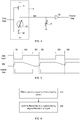
- FIG. 1 is a waveform diagram of pulse-width modulated data.
- FIG. 1 illustrates the waveforms used with M-PHY, but other waveforms may be used with different polarities and different bit definitions.
- the data signal transitions from high to low.
- a ZERO data value is represented by a pulse with a low time that is wider than the high time.
- a ONE data value is represented by a pulse with a high time that is wider than the low time.
- the width of the wide pulses may be, for example, two-thirds of the bit time.
- Communication on an M-PHY link can occur in bursts.
- the bursts include various states including a synchronization (SYNC) state that has a data sequence useful for synchronizing a receiver to a transmitter.
- the SYNC state may, for example, have a high density of transitions between data values.
- User data is communicated in a PAYLOAD state made up of 8B10B (8 data bits coded as 10 pulse-width modulated bits) coded symbols.
- a decoder may sample the data input 12 times per bit time and analyze the samples to determine the received data values. This type of decoder may not be suitable to use at the higher gears.
- Published U.S. Patent Application US 2010/0260283 A1 relates to a duty-cycle modulated bit signaling method and circuit where values are signaled bits by virtue of a duty-cycle ratio and the duty-cycle ratio is varied dependent upon the transmission rate of the signaling.
- a bit period includes a long phase and a short phase and the duty-cycle is varied such that the ratio between the duration of the long phase and the duration of the short phase is increased for decreasing transmission rate.
- the duty-cycle ratio is varied dependent upon the transmission rate of the signaling according to one or more ranges of transmission rate. In a higher transmission rate range the duty-cycle is defined as a fixed ratio, and in a lower transmission range the duty-cycle is defined by a fixed length of the short phase of the bit period.
- a receiver includes an edge detector to detect a first falling edge and a first rising edge of an input signal received from a transmitter and a counter that counts in a first direction in response to detecting the first falling edge and that counts in a second direction in response to detecting the first rising edge of the input signal.
- the counter generates a final count value based on the counts in the first and second directions.
- the receiver includes a decision unit to determine whether data in the input signal is of logical high or logical low value with the determination made according to the final count value.
- a decoder for decoding pulse-width modulated data from a data input signal, the data input signal containing a serial stream of bits, each bit of the serial stream spanning a bit time, each bit of the serial stream having a high pulse whose duration signals the value of the respective bit.
- the decoder includes a one-sided pulse filter configured to produce a filtered data signal by shortening the durations of high pulses on the data input signal; and a flip-flop configured to latch the filtered data signal at the end of each bit time of the data input signal.
- a method for decoding pulse-width modulated data from a data input signal, the data input signal containing a serial stream of bits, each bit of the serial stream spanning a bit time, each bit of the serial stream having a trailing pulse whose duration signals the value of the respective bit.
- the method includes filtering the data input signal to shorten the trailing pulses; and latching the filtered data input signal on trailing edges of the data input signal.
- an apparatus for decoding pulse-width modulated data from a data input signal, the data input signal containing a serial stream of bits, each bit of the serial stream spanning a bit time, each bit of the serial stream having a trailing pulse whose duration signals the value of the respective bit.
- the apparatus includes a means for filtering the data input signal to shorten trailing pulses; and a means for latching the filtered data input signal on trailing edges of the data input signal.
- FIG. 2 is a functional block diagram of a PWM decoder according to a presently disclosed embodiment.
- the PWM decoder can be implemented in many different ways.
- the PWM decoder is implemented in a complementary metal oxide semiconductor (CMOS) integrated circuit.
- CMOS complementary metal oxide semiconductor
- the decoder receives a serial stream of data on a data input signal (Data Input).
- Data Input The data input signal is pulse-width modulated, for example, using waveforms as illustrated in FIG. 1 .
- the decoder decodes the data in the data input signal to produce a data output signal (Data Output) that signals the values of the PWM-coded data in the data input signal.
- Data Output data output signal
- the PWM decoder can also supply a clock output signal (Clock Output) that signals the timing of the data output signal.
- the decoder includes a one-sided pulse filter 20 that receives the data input signal and produces a filtered data signal (Filtered Data).
- the one-sided pulse filter 20 shortens (or chops) the high time of pulses that it receives.
- the amount of pulse shortening by the one-sided pulse filter 20 is set so that the high pulse of a PWM data ZERO bit is completely suppressed and the filtered data signal remains low during the bit time of a data ZERO and that the active pulse of a PWM data ONE bit is not completely suppressed and the filtered data signal transitions high during the bit time of a data ONE.
- the one-sided pulse filter 20 may be viewed as a buffer that has different input-to-output delays for rising transitions and falling transitions. Accordingly, the one-sided pulse filter 20 may be referred to as an asymmetric filter.
- the delay for rising transitions is greater than the delay for falling transitions so that the duration of high pulses is shortened.
- the delay for falling transitions may be short, for example, a few gate delays.
- Signal transitions may also be referred to as edges; for example, a rising transition may also be referred to as a rising edge and a falling transition may be referred to as a falling edge. Similarly, a rising transition may be referred to as a transition from a low level to a high level and a falling transition may be referred to as a transition from a high level to a low level.
- the decoder may calibrate the delay for rising transitions before receiving user data. Calibrating the delay for rising transitions provides calibration of the durations of high pulses that are suppressed. For example, the delay may be calibrated during the synchronization state of a received M-PHY data signal.
- the calibration may, for example, include sweeping through a range of possible delay values. Some of the delay values, those with delays that are too long, will result in the data output signal being all ZEROs. Other delay values, those with delays that are too short, will result in the data output signal being all ONEs.
- the calibration may, for example, select a delay midway between the lowest delay value that is too high and the highest delay value that is too low.
- the calibration may also look for particular output values based on the expected pattern in the synchronization state.
- a calibration module can monitor the data output signal during the synchronization (SYNC) state. Based on the values of the data output signal, the calibration module may adjust delay settings such that the data output signal is no longer constant ZEROs or ONEs.
- the calibration module can also check for a data pattern that is 8B10B encoded and has at least one transition every 3 bit times.
- the filtered data signal from the one-sided pulse filter 20 is captured in a flip-flop 45.
- the flip-flop 45 has a data input (D) connected to the filtered data signal, a clock input connected to the clock output signal, and a data output (Q) connected to the data output signal of the decoder.
- a clock generator module 30 supplies the clock output signal.
- the clock generator module 30 includes an inverter 35.
- the clock generator module 30 produces the clock output signal from the data input signal.
- the inverter 35 has an input connected to the data input signal and an output connected to the clock output signal.
- the clock output signal is the logical complement of the data input signal.
- the clock generator module 30 may include other circuitry, for example, based on the characteristics of the flip-flop 45.
- the clock generator module 30 and the one-sided pulse filter 20 can be designed so that their delays satisfy timing requirements of the flip-flop 45. For example, the minimum delay from input-to-output of the one-sided pulse filter 20 for falling transitions should be long enough (relative to the delay of the clock generator module 30) to satisfy a hold time requirement of the flip-flop 45.
- FIG. 3 is a waveform diagram illustrating operation of the PWM decoder of FIG. 2.
- FIG. 3 illustrates a data ONE bit time from time 301 to time 304 and a data ZERO bit time from time 304 to time 306.
- the waveforms are illustrated for circuit delays that are small relative to a bit time and signal transitions that are instantaneous.
- the data input signal falls and shortly thereafter the filtered data signal also falls.
- the delay time from the falling of the data input signal to the falling of the filtered data signal is the delay of the one-sided pulse filter 20 for falling transitions.
- the data input signal rises.
- the filtered data signal rises.
- the delay from time 302 to time 303 is the delay of the one-sided pulse filter 20 for rising transitions.
- the end of the data ONE bit time the data input signal falls and the clock output signal rises.
- the rising edge of the clock output signal triggers the flip-flop 45 to latch the filtered data signal. Since the filtered data signal is high at this time, the data output is set to a ONE, which matches the PWM coded value of the data input signal.
- the data input signal falls and shortly thereafter the filtered data signal falls as at time 301.
- the data input signal rises.
- the end of the data ZERO bit time the data input signal falls and the clock output signal rises.
- the active time of the data input signal from time 305 to time 306, is shorter than the delay of the one-sided pulse filter 20 for rising transitions.
- the filtered data signal remains low.
- the rising edge of the clock output signal triggers the flip-flop 45 to latch the filtered data signal. Since the filter data signal is low at this time, the data output is set to a ZERO, which matches the PWM coded value of the data input signal.
- FIG. 4 is a schematic diagram of a one-sided pulse filter according to a presently disclosed embodiment.
- the one-sided pulse filter may be used as the one-sided pulse filter 20 in the decoder of FIG. 2 .
- the one-sided pulse filter of FIG. 4 receives the data input signal and produces the filtered data signal with shortened high times of pulses.
- the one-sided pulse filter uses a current discharging a capacitor 27 to control the amount of pulse shortening.
- the current is from a current source 25 that switchably discharges the capacitor 27 based on the data input signal.
- the one-sided pulse filter includes a first inverter 24 made up of a p-channel transistor 21, the current source 25, and an n-channel transistor 22.
- the output of the inverter is connected to a midpoint (Mid) of the one-sided pulse filter.
- a second inverter 29 has its input connected to the midpoint and its output connected to the filtered data signal.
- the p-channel transistor 21 has its gate connected to the data input signal, its source connected to a voltage supply, and its drain connected to the output of the first inverter 24.
- the n-channel transistor 22 has its gate connected to the data input signal and its source connected to a ground reference.
- the n-channel transistor 22 has its drain connected to a terminal of the current source 25 whose other terminal is connected to the output of the first inverter 24.
- the channel of the n-channel transistor 22 is in series with the current source 25.
- the current source 25 may be connected to the ground reference and the drain of the n-channel transistor 22 connected to the midpoint of the one-sided pulse filter. The current source 25 discharges the capacitor 27 when the data input signal is high.
- the amount of shortening of pulses (the delay for rising transitions) is controlled by the current of the current source 25 and the capacitance of the capacitor 27.
- the delay for rising transitions is based on the product of the current of the current source 25 and the capacitance of the capacitor 27.
- One or both of the current source 25 and the capacitor 27 are variable so that the amount of pulse shortening can be adjusted for calibration and for different gears.
- the calibration may include adjusting a digital value.
- the current source 25 may include a current-mode digital-to-analog converter.
- the capacitor 27 may include, for example, multiple capacitors that are switchably connected to the midpoint of the one-sided pulse filter.
- the range of delay adjustment can be chosen based on the range of data rates that the PWM decoder will be used with. For example, if the PWM decoder will be used in gear 6 of M-PHY, the range of delay adjustments may be greater than a factor of 3. The range of data rates for gear 6 spans a factor of 3. The adjustment range of the one-sided pulse filter may be greater than a factor of 3, for example, to include variations in process, voltage, and temperature. For another example, if the PWM decoder will be used in gears 6 and 7 of M-PHY, the range of the day delay adjustments may be greater than a factor of 6 (which is the ratio of the minimum data rate in gear 6 to the maximum data rate in gear 7).
- FIG. 5 is a waveform diagram illustrating operation of the one-sided pulse filter of FIG. 4.
- FIG. 5 illustrates a data ONE bit time from time 501 to time 504 and a data ZERO bit time from time 504 to time 506.
- the data input signal falls. This turns on p-channel transistor 21 and pulls the midpoint high.
- the high-level on the midpoint causes the second inverter 29 to switch and drive the filtered data signal low.
- the delay time from the falling of the data input signal to the falling of the filtered data signal is the delay of the one-sided pulse filter for falling transitions. This delay will be short when the p-channel transistor 21 is able to rapidly charge the capacitor 27.
- the data input signal rises. This turns off p-channel transistor 21 and turns on n-channel transistor 22 which enables the current source 25 to discharge the capacitor 27.
- the voltage on the midpoint will ramp downward at a rate determined by the current source 25 and the capacitor 27.
- the midpoint has ramped to a level that causes the second inverter 29 to switch. Accordingly, at time 503 the filtered data signal switches high.
- the delay from time 502 to time 503 is the delay of the one-sided pulse filter for rising transitions.
- the filtered data signal remains high through the end of the data ONE bit time.
- the data input signal falls. As described for time 501, this causes the filtered data signal to fall.
- the data input signal rises. This turns off p-channel transistor 21 and turns on n-channel transistor 22, which enables the current source 25 to discharge the capacitor 27.
- the voltage on the midpoint will ramp downward at a rate determined by the current source 25 and the capacitor 27.
- the data input signal falls. At this time, the midpoint has not ramped downward enough to cause the second inverter 29 to switch. Accordingly, at time 503 the filtered data signal remains low through the end of the data ZERO bit time.
- the transition (falling in FIG. 1 ) at the beginning of the bit time may be referred to as a leading edge, and the transition (falling in FIG. 1 ) at the end of the bit time may be referred to as a trailing edge.
- the pulse (low in FIG. 1 ) at the beginning of the bit time may at be referred to as a leading pulse, and the pulse (high in FIG. 1 ) at the end of the bit time may be referred to as a trailing pulse.
- the pulses within a bit time may be referenced by their duration for example using terms such as narrow, wide, short, or long.
- Variations in the decoder of FIG. 2 can work with other signal polarity and bit-value definitions.
- the one-sided pulse filter 20 can be configured to shorten (or chop) the duration of the trailing pulses that it receives.
- the one-sided pulse filter 20 suppresses short trailing pulses and passes (albeit with a shorter duration) long trailing pulses.
- the flip-flop 45 can be configured to latch the filtered data signal on the trailing edges of the data input signal.
- FIG. 6 is a flowchart of a process for decoding pulse-width modulated data according to a presently disclosed embodiment. The process may be implemented, for example, using the PWM decoder of FIG. 2 .
- step 610 the process filtering the data input signal to shorten trailing pulses.
- the filtering suppresses short trailing pulses on the data input signal but does not suppress long trailing pulses on the data input signal.
- the durations of pulses that suppress may be determined by calibration.
- the one-sided pulse filter 20 of the decoder of FIG. 2 may be used to filter the data input signal.
- step 620 the process latches the filtered data input signal (from step 610) on trailing edges of the data input signal.
- the flip-flop 45 of the decoder of FIG. 2 may latch the output of the one-sided pulse filter 20 on falling edges of the data input signal.
- the process may also include generating a clock output signal from the data input signal and using the clock output signal to trigger latching the filtered data input signal.
- FIG. 6 may be modified, for example, by adding or altering steps. Additionally, steps may be performed concurrently.
Landscapes
- Engineering & Computer Science (AREA)
- General Engineering & Computer Science (AREA)
- Theoretical Computer Science (AREA)
- Physics & Mathematics (AREA)
- Computer Hardware Design (AREA)
- General Physics & Mathematics (AREA)
- Spectroscopy & Molecular Physics (AREA)
- Computer Networks & Wireless Communication (AREA)
- Signal Processing (AREA)
- Dc Digital Transmission (AREA)
- Analogue/Digital Conversion (AREA)
- Compression, Expansion, Code Conversion, And Decoders (AREA)
- Synchronisation In Digital Transmission Systems (AREA)
Applications Claiming Priority (2)
| Application Number | Priority Date | Filing Date | Title |
|---|---|---|---|
| US14/258,980 US9203391B2 (en) | 2014-04-22 | 2014-04-22 | Pulse-width modulation data decoder |
| PCT/US2015/020027 WO2015163989A1 (en) | 2014-04-22 | 2015-03-11 | Pulse-width modulation data decoder |
Publications (2)
| Publication Number | Publication Date |
|---|---|
| EP3134818A1 EP3134818A1 (en) | 2017-03-01 |
| EP3134818B1 true EP3134818B1 (en) | 2018-05-02 |
Family
ID=52774569
Family Applications (1)
| Application Number | Title | Priority Date | Filing Date |
|---|---|---|---|
| EP15713079.0A Active EP3134818B1 (en) | 2014-04-22 | 2015-03-11 | Pulse-width modulation data decoder |
Country Status (7)
Families Citing this family (9)
| Publication number | Priority date | Publication date | Assignee | Title |
|---|---|---|---|---|
| CN109213436B (zh) | 2017-06-30 | 2021-08-24 | 慧荣科技股份有限公司 | 降低快闪储存介面中传收数据错误方法及装置 |
| TWI645298B (zh) * | 2017-06-30 | 2018-12-21 | 慧榮科技股份有限公司 | 降低快閃儲存介面中傳收資料錯誤方法以及使用該方法的裝置 |
| US10848263B2 (en) | 2017-06-30 | 2020-11-24 | Silicon Motion, Inc. | Methods for reducing data errors in transceiving of a flash storage interface and apparatuses using the same |
| US10630424B2 (en) | 2017-06-30 | 2020-04-21 | Silicon Motion, Inc. | Methods for reducing data errors in transceiving of a flash storage interface and apparatuses using the same |
| US10637509B2 (en) | 2017-06-30 | 2020-04-28 | Silicon Motion, Inc. | Methods for reducing data errors in transceiving of a flash storage interface and apparatuses using the same |
| US10050674B1 (en) * | 2017-07-18 | 2018-08-14 | Bendix Commercial Vehicle Systems Llc | System and method for controlling power line communications between members of a tractor-trailer |
| KR102660412B1 (ko) * | 2018-10-30 | 2024-04-25 | 에스케이하이닉스 주식회사 | 주파수 감지 회로 |
| US10904048B2 (en) | 2019-05-24 | 2021-01-26 | SanDiskTechnologies LLC | Pulse width modulated receiver systems and methods |
| CN115150004B (zh) * | 2022-07-01 | 2024-02-13 | 国仪量子技术(合肥)股份有限公司 | 一种窄脉冲发生器 |
Family Cites Families (14)
| Publication number | Priority date | Publication date | Assignee | Title |
|---|---|---|---|---|
| US4216426A (en) * | 1979-03-02 | 1980-08-05 | Burroughs Corporation | Self-clocked data transmission system having automatic signal reversing means |
| US5438303A (en) | 1992-07-14 | 1995-08-01 | Sony Corporation | Pulse with modulation apparatus with plural independably controllable variable delay devices |
| KR950004058A (ko) | 1993-07-30 | 1995-02-17 | 오오가 노리오 | 펄스폭 변조회로 |
| US5696800A (en) | 1995-03-22 | 1997-12-09 | Intel Corporation | Dual tracking differential manchester decoder and clock recovery circuit |
| KR100938958B1 (ko) | 2001-05-24 | 2010-01-26 | 에트링크스 유에스에이, 인크. | 협대역 카오스 주파수 시프트 키잉 |
| US7359313B2 (en) * | 2002-06-24 | 2008-04-15 | Agere Systems Inc. | Space-time bit-interleaved coded modulation for wideband transmission |
| KR100515472B1 (ko) * | 2002-10-15 | 2005-09-16 | 브이케이 주식회사 | 채널 부호화, 복호화 방법 및 이를 수행하는 다중 안테나무선통신 시스템 |
| US8095104B2 (en) * | 2006-06-30 | 2012-01-10 | Semiconductor Energy Laboratory Co., Ltd. | Semiconductor device and electronic device having the same |
| EP2210382A2 (en) * | 2007-11-13 | 2010-07-28 | Nxp B.V. | Duty-cycle modulated transmission |
| KR101214035B1 (ko) | 2008-09-04 | 2012-12-20 | 가부시키가이샤 어드밴티스트 | 시험 장치, 송신 장치, 수신 장치, 시험 방법, 송신 방법, 및 수신 방법 |
| US20110235763A1 (en) * | 2009-01-12 | 2011-09-29 | Rambus Inc. | Signaling system with asymmetrically-managed timing calibration |
| JP2010283628A (ja) * | 2009-06-05 | 2010-12-16 | Yamaha Corp | 同期信号発生回路 |
| DE112011105674T5 (de) | 2011-09-28 | 2014-07-17 | Intel Corp. | Datenwiederherstellung bei niedriger Energie unter Verwendung von Übertaktung |
| US8847691B2 (en) * | 2011-11-16 | 2014-09-30 | Qualcomm Incorporated | Apparatus and method for recovering burst-mode pulse width modulation (PWM) and non-return-to-zero (NRZ) data |
-
2014
- 2014-04-22 US US14/258,980 patent/US9203391B2/en not_active Expired - Fee Related
-
2015
- 2015-03-11 CN CN201580020491.9A patent/CN106233272A/zh active Pending
- 2015-03-11 KR KR1020167028843A patent/KR101873864B1/ko not_active Expired - Fee Related
- 2015-03-11 JP JP2016563826A patent/JP6370922B2/ja not_active Expired - Fee Related
- 2015-03-11 BR BR112016024711A patent/BR112016024711A2/pt not_active IP Right Cessation
- 2015-03-11 EP EP15713079.0A patent/EP3134818B1/en active Active
- 2015-03-11 WO PCT/US2015/020027 patent/WO2015163989A1/en active Application Filing
Non-Patent Citations (1)
| Title |
|---|
| None * |
Also Published As
| Publication number | Publication date |
|---|---|
| US20150303910A1 (en) | 2015-10-22 |
| US9203391B2 (en) | 2015-12-01 |
| BR112016024711A2 (pt) | 2017-08-15 |
| JP2017517941A (ja) | 2017-06-29 |
| KR101873864B1 (ko) | 2018-07-03 |
| EP3134818A1 (en) | 2017-03-01 |
| WO2015163989A1 (en) | 2015-10-29 |
| KR20160145590A (ko) | 2016-12-20 |
| JP6370922B2 (ja) | 2018-08-08 |
| CN106233272A (zh) | 2016-12-14 |
Similar Documents
| Publication | Publication Date | Title |
|---|---|---|
| EP3134818B1 (en) | Pulse-width modulation data decoder | |
| EP2798742B1 (en) | Forwarded clock jitter reduction | |
| US8090068B2 (en) | System and method of calibrating power-on gating window for a time-to-digital converter (TDC) of a digital phase locked loop (DPLL) | |
| US9030244B1 (en) | Clock duty cycle calibration circuitry | |
| CN105612763B (zh) | 用于数字麦克风的转换速率控制装置 | |
| US10128825B2 (en) | Ringing suppression circuit | |
| JP6429205B2 (ja) | バスシステムの加入者局、及び、バスシステム内の導線に関係する放射量を低減する方法 | |
| US20150304136A1 (en) | Partial Response Receiver And Related Method | |
| US9356589B2 (en) | Interchannel skew adjustment circuit | |
| WO2014133783A1 (en) | Phase-locked loop using dual loop mode to achieve fast resettling | |
| US12218699B2 (en) | Receiver circuit and receiver circuit control method | |
| KR20100007899A (ko) | 코스 타이밍 소스로부터 파인 타이밍을 생성하기 위한 장치 및 방법 | |
| EP3062454A1 (en) | Optical link clock receiver | |
| CN115133764A (zh) | 低EMI高频Buck控制器电路 | |
| TW200934128A (en) | Filter and filtering method | |
| CN210780702U (zh) | 一种滤波电路 | |
| EP2478638A1 (en) | Delay-locked loop having a delay independent of input signal duty cycle variation | |
| JP6404012B2 (ja) | 信号処理装置 | |
| KR20040073300A (ko) | 서로 상보인 두 개의 클럭 신호를 이용하여 통신을 행하는통신 장치 | |
| EP3114805B1 (en) | Systems and methods for frequency detection | |
| US20070116163A1 (en) | Receiving circuit for multi-slot receiving provided with circuit for adjusting frequency characteristic of active filter | |
| TWI412253B (zh) | 通信電路及其方法 | |
| US7035349B2 (en) | Signal compensation circuit and demodulating circuit with high-speed and low-speed feedback loops | |
| KR20170086975A (ko) | 차량용 통신 송수신기의 기울기 제어 회로 및 이를 이용한 기울기 제어 방법 | |
| JP3180650B2 (ja) | Eeprom自動読み出し装置 |
Legal Events
| Date | Code | Title | Description |
|---|---|---|---|
| STAA | Information on the status of an ep patent application or granted ep patent |
Free format text: STATUS: THE INTERNATIONAL PUBLICATION HAS BEEN MADE |
|
| PUAI | Public reference made under article 153(3) epc to a published international application that has entered the european phase |
Free format text: ORIGINAL CODE: 0009012 |
|
| STAA | Information on the status of an ep patent application or granted ep patent |
Free format text: STATUS: REQUEST FOR EXAMINATION WAS MADE |
|
| 17P | Request for examination filed |
Effective date: 20160913 |
|
| AK | Designated contracting states |
Kind code of ref document: A1 Designated state(s): AL AT BE BG CH CY CZ DE DK EE ES FI FR GB GR HR HU IE IS IT LI LT LU LV MC MK MT NL NO PL PT RO RS SE SI SK SM TR |
|
| AX | Request for extension of the european patent |
Extension state: BA ME |
|
| DAV | Request for validation of the european patent (deleted) | ||
| DAX | Request for extension of the european patent (deleted) | ||
| GRAP | Despatch of communication of intention to grant a patent |
Free format text: ORIGINAL CODE: EPIDOSNIGR1 |
|
| STAA | Information on the status of an ep patent application or granted ep patent |
Free format text: STATUS: GRANT OF PATENT IS INTENDED |
|
| INTG | Intention to grant announced |
Effective date: 20171128 |
|
| GRAS | Grant fee paid |
Free format text: ORIGINAL CODE: EPIDOSNIGR3 |
|
| GRAA | (expected) grant |
Free format text: ORIGINAL CODE: 0009210 |
|
| STAA | Information on the status of an ep patent application or granted ep patent |
Free format text: STATUS: THE PATENT HAS BEEN GRANTED |
|
| AK | Designated contracting states |
Kind code of ref document: B1 Designated state(s): AL AT BE BG CH CY CZ DE DK EE ES FI FR GB GR HR HU IE IS IT LI LT LU LV MC MK MT NL NO PL PT RO RS SE SI SK SM TR |
|
| REG | Reference to a national code |
Ref country code: GB Ref legal event code: FG4D |
|
| REG | Reference to a national code |
Ref country code: CH Ref legal event code: EP Ref country code: AT Ref legal event code: REF Ref document number: 995992 Country of ref document: AT Kind code of ref document: T Effective date: 20180515 |
|
| REG | Reference to a national code |
Ref country code: DE Ref legal event code: R096 Ref document number: 602015010702 Country of ref document: DE Ref country code: IE Ref legal event code: FG4D |
|
| REG | Reference to a national code |
Ref country code: NL Ref legal event code: MP Effective date: 20180502 |
|
| REG | Reference to a national code |
Ref country code: LT Ref legal event code: MG4D |
|
| PG25 | Lapsed in a contracting state [announced via postgrant information from national office to epo] |
Ref country code: BG Free format text: LAPSE BECAUSE OF FAILURE TO SUBMIT A TRANSLATION OF THE DESCRIPTION OR TO PAY THE FEE WITHIN THE PRESCRIBED TIME-LIMIT Effective date: 20180802 Ref country code: NO Free format text: LAPSE BECAUSE OF FAILURE TO SUBMIT A TRANSLATION OF THE DESCRIPTION OR TO PAY THE FEE WITHIN THE PRESCRIBED TIME-LIMIT Effective date: 20180802 Ref country code: FI Free format text: LAPSE BECAUSE OF FAILURE TO SUBMIT A TRANSLATION OF THE DESCRIPTION OR TO PAY THE FEE WITHIN THE PRESCRIBED TIME-LIMIT Effective date: 20180502 Ref country code: SE Free format text: LAPSE BECAUSE OF FAILURE TO SUBMIT A TRANSLATION OF THE DESCRIPTION OR TO PAY THE FEE WITHIN THE PRESCRIBED TIME-LIMIT Effective date: 20180502 Ref country code: ES Free format text: LAPSE BECAUSE OF FAILURE TO SUBMIT A TRANSLATION OF THE DESCRIPTION OR TO PAY THE FEE WITHIN THE PRESCRIBED TIME-LIMIT Effective date: 20180502 Ref country code: LT Free format text: LAPSE BECAUSE OF FAILURE TO SUBMIT A TRANSLATION OF THE DESCRIPTION OR TO PAY THE FEE WITHIN THE PRESCRIBED TIME-LIMIT Effective date: 20180502 |
|
| PG25 | Lapsed in a contracting state [announced via postgrant information from national office to epo] |
Ref country code: NL Free format text: LAPSE BECAUSE OF FAILURE TO SUBMIT A TRANSLATION OF THE DESCRIPTION OR TO PAY THE FEE WITHIN THE PRESCRIBED TIME-LIMIT Effective date: 20180502 Ref country code: LV Free format text: LAPSE BECAUSE OF FAILURE TO SUBMIT A TRANSLATION OF THE DESCRIPTION OR TO PAY THE FEE WITHIN THE PRESCRIBED TIME-LIMIT Effective date: 20180502 Ref country code: RS Free format text: LAPSE BECAUSE OF FAILURE TO SUBMIT A TRANSLATION OF THE DESCRIPTION OR TO PAY THE FEE WITHIN THE PRESCRIBED TIME-LIMIT Effective date: 20180502 Ref country code: HR Free format text: LAPSE BECAUSE OF FAILURE TO SUBMIT A TRANSLATION OF THE DESCRIPTION OR TO PAY THE FEE WITHIN THE PRESCRIBED TIME-LIMIT Effective date: 20180502 Ref country code: GR Free format text: LAPSE BECAUSE OF FAILURE TO SUBMIT A TRANSLATION OF THE DESCRIPTION OR TO PAY THE FEE WITHIN THE PRESCRIBED TIME-LIMIT Effective date: 20180803 |
|
| REG | Reference to a national code |
Ref country code: AT Ref legal event code: MK05 Ref document number: 995992 Country of ref document: AT Kind code of ref document: T Effective date: 20180502 |
|
| PG25 | Lapsed in a contracting state [announced via postgrant information from national office to epo] |
Ref country code: EE Free format text: LAPSE BECAUSE OF FAILURE TO SUBMIT A TRANSLATION OF THE DESCRIPTION OR TO PAY THE FEE WITHIN THE PRESCRIBED TIME-LIMIT Effective date: 20180502 Ref country code: PL Free format text: LAPSE BECAUSE OF FAILURE TO SUBMIT A TRANSLATION OF THE DESCRIPTION OR TO PAY THE FEE WITHIN THE PRESCRIBED TIME-LIMIT Effective date: 20180502 Ref country code: RO Free format text: LAPSE BECAUSE OF FAILURE TO SUBMIT A TRANSLATION OF THE DESCRIPTION OR TO PAY THE FEE WITHIN THE PRESCRIBED TIME-LIMIT Effective date: 20180502 Ref country code: CZ Free format text: LAPSE BECAUSE OF FAILURE TO SUBMIT A TRANSLATION OF THE DESCRIPTION OR TO PAY THE FEE WITHIN THE PRESCRIBED TIME-LIMIT Effective date: 20180502 Ref country code: AT Free format text: LAPSE BECAUSE OF FAILURE TO SUBMIT A TRANSLATION OF THE DESCRIPTION OR TO PAY THE FEE WITHIN THE PRESCRIBED TIME-LIMIT Effective date: 20180502 Ref country code: SK Free format text: LAPSE BECAUSE OF FAILURE TO SUBMIT A TRANSLATION OF THE DESCRIPTION OR TO PAY THE FEE WITHIN THE PRESCRIBED TIME-LIMIT Effective date: 20180502 Ref country code: DK Free format text: LAPSE BECAUSE OF FAILURE TO SUBMIT A TRANSLATION OF THE DESCRIPTION OR TO PAY THE FEE WITHIN THE PRESCRIBED TIME-LIMIT Effective date: 20180502 |
|
| REG | Reference to a national code |
Ref country code: DE Ref legal event code: R097 Ref document number: 602015010702 Country of ref document: DE |
|
| PG25 | Lapsed in a contracting state [announced via postgrant information from national office to epo] |
Ref country code: SM Free format text: LAPSE BECAUSE OF FAILURE TO SUBMIT A TRANSLATION OF THE DESCRIPTION OR TO PAY THE FEE WITHIN THE PRESCRIBED TIME-LIMIT Effective date: 20180502 Ref country code: IT Free format text: LAPSE BECAUSE OF FAILURE TO SUBMIT A TRANSLATION OF THE DESCRIPTION OR TO PAY THE FEE WITHIN THE PRESCRIBED TIME-LIMIT Effective date: 20180502 |
|
| PLBE | No opposition filed within time limit |
Free format text: ORIGINAL CODE: 0009261 |
|
| STAA | Information on the status of an ep patent application or granted ep patent |
Free format text: STATUS: NO OPPOSITION FILED WITHIN TIME LIMIT |
|
| 26N | No opposition filed |
Effective date: 20190205 |
|
| PG25 | Lapsed in a contracting state [announced via postgrant information from national office to epo] |
Ref country code: SI Free format text: LAPSE BECAUSE OF FAILURE TO SUBMIT A TRANSLATION OF THE DESCRIPTION OR TO PAY THE FEE WITHIN THE PRESCRIBED TIME-LIMIT Effective date: 20180502 |
|
| PG25 | Lapsed in a contracting state [announced via postgrant information from national office to epo] |
Ref country code: MC Free format text: LAPSE BECAUSE OF FAILURE TO SUBMIT A TRANSLATION OF THE DESCRIPTION OR TO PAY THE FEE WITHIN THE PRESCRIBED TIME-LIMIT Effective date: 20180502 |
|
| REG | Reference to a national code |
Ref country code: CH Ref legal event code: PL |
|
| GBPC | Gb: european patent ceased through non-payment of renewal fee |
Effective date: 20190311 |
|
| PG25 | Lapsed in a contracting state [announced via postgrant information from national office to epo] |
Ref country code: LU Free format text: LAPSE BECAUSE OF NON-PAYMENT OF DUE FEES Effective date: 20190311 Ref country code: AL Free format text: LAPSE BECAUSE OF FAILURE TO SUBMIT A TRANSLATION OF THE DESCRIPTION OR TO PAY THE FEE WITHIN THE PRESCRIBED TIME-LIMIT Effective date: 20180502 |
|
| REG | Reference to a national code |
Ref country code: BE Ref legal event code: MM Effective date: 20190331 |
|
| PG25 | Lapsed in a contracting state [announced via postgrant information from national office to epo] |
Ref country code: IE Free format text: LAPSE BECAUSE OF NON-PAYMENT OF DUE FEES Effective date: 20190311 Ref country code: CH Free format text: LAPSE BECAUSE OF NON-PAYMENT OF DUE FEES Effective date: 20190331 Ref country code: LI Free format text: LAPSE BECAUSE OF NON-PAYMENT OF DUE FEES Effective date: 20190331 Ref country code: GB Free format text: LAPSE BECAUSE OF NON-PAYMENT OF DUE FEES Effective date: 20190311 |
|
| PG25 | Lapsed in a contracting state [announced via postgrant information from national office to epo] |
Ref country code: BE Free format text: LAPSE BECAUSE OF NON-PAYMENT OF DUE FEES Effective date: 20190331 Ref country code: FR Free format text: LAPSE BECAUSE OF NON-PAYMENT OF DUE FEES Effective date: 20190331 |
|
| PG25 | Lapsed in a contracting state [announced via postgrant information from national office to epo] |
Ref country code: TR Free format text: LAPSE BECAUSE OF FAILURE TO SUBMIT A TRANSLATION OF THE DESCRIPTION OR TO PAY THE FEE WITHIN THE PRESCRIBED TIME-LIMIT Effective date: 20180502 |
|
| PG25 | Lapsed in a contracting state [announced via postgrant information from national office to epo] |
Ref country code: MT Free format text: LAPSE BECAUSE OF NON-PAYMENT OF DUE FEES Effective date: 20190311 Ref country code: PT Free format text: LAPSE BECAUSE OF FAILURE TO SUBMIT A TRANSLATION OF THE DESCRIPTION OR TO PAY THE FEE WITHIN THE PRESCRIBED TIME-LIMIT Effective date: 20180903 |
|
| PG25 | Lapsed in a contracting state [announced via postgrant information from national office to epo] |
Ref country code: CY Free format text: LAPSE BECAUSE OF FAILURE TO SUBMIT A TRANSLATION OF THE DESCRIPTION OR TO PAY THE FEE WITHIN THE PRESCRIBED TIME-LIMIT Effective date: 20180502 |
|
| PG25 | Lapsed in a contracting state [announced via postgrant information from national office to epo] |
Ref country code: IS Free format text: LAPSE BECAUSE OF FAILURE TO SUBMIT A TRANSLATION OF THE DESCRIPTION OR TO PAY THE FEE WITHIN THE PRESCRIBED TIME-LIMIT Effective date: 20180902 |
|
| PG25 | Lapsed in a contracting state [announced via postgrant information from national office to epo] |
Ref country code: HU Free format text: LAPSE BECAUSE OF FAILURE TO SUBMIT A TRANSLATION OF THE DESCRIPTION OR TO PAY THE FEE WITHIN THE PRESCRIBED TIME-LIMIT; INVALID AB INITIO Effective date: 20150311 |
|
| PG25 | Lapsed in a contracting state [announced via postgrant information from national office to epo] |
Ref country code: MK Free format text: LAPSE BECAUSE OF FAILURE TO SUBMIT A TRANSLATION OF THE DESCRIPTION OR TO PAY THE FEE WITHIN THE PRESCRIBED TIME-LIMIT Effective date: 20180502 |
|
| PGFP | Annual fee paid to national office [announced via postgrant information from national office to epo] |
Ref country code: DE Payment date: 20250210 Year of fee payment: 11 |