EP3133633B1 - Studying dynamic specimen behavior in a charged-particle microscope - Google Patents
Studying dynamic specimen behavior in a charged-particle microscope Download PDFInfo
- Publication number
- EP3133633B1 EP3133633B1 EP16157199.7A EP16157199A EP3133633B1 EP 3133633 B1 EP3133633 B1 EP 3133633B1 EP 16157199 A EP16157199 A EP 16157199A EP 3133633 B1 EP3133633 B1 EP 3133633B1
- Authority
- EP
- European Patent Office
- Prior art keywords
- specimen
- deflecting device
- pulses
- train
- array
- Prior art date
- Legal status (The legal status is an assumption and is not a legal conclusion. Google has not performed a legal analysis and makes no representation as to the accuracy of the status listed.)
- Active
Links
Images

Classifications
-
- H—ELECTRICITY
- H01—ELECTRIC ELEMENTS
- H01J—ELECTRIC DISCHARGE TUBES OR DISCHARGE LAMPS
- H01J37/00—Discharge tubes with provision for introducing objects or material to be exposed to the discharge, e.g. for the purpose of examination or processing thereof
- H01J37/26—Electron or ion microscopes; Electron or ion diffraction tubes
- H01J37/261—Details
-
- H—ELECTRICITY
- H01—ELECTRIC ELEMENTS
- H01J—ELECTRIC DISCHARGE TUBES OR DISCHARGE LAMPS
- H01J37/00—Discharge tubes with provision for introducing objects or material to be exposed to the discharge, e.g. for the purpose of examination or processing thereof
- H01J37/02—Details
- H01J37/04—Arrangements of electrodes and associated parts for generating or controlling the discharge, e.g. electron-optical arrangement or ion-optical arrangement
- H01J37/045—Beam blanking or chopping, i.e. arrangements for momentarily interrupting exposure to the discharge
-
- H—ELECTRICITY
- H01—ELECTRIC ELEMENTS
- H01J—ELECTRIC DISCHARGE TUBES OR DISCHARGE LAMPS
- H01J37/00—Discharge tubes with provision for introducing objects or material to be exposed to the discharge, e.g. for the purpose of examination or processing thereof
- H01J37/02—Details
- H01J37/04—Arrangements of electrodes and associated parts for generating or controlling the discharge, e.g. electron-optical arrangement or ion-optical arrangement
- H01J37/147—Arrangements for directing or deflecting the discharge along a desired path
- H01J37/1472—Deflecting along given lines
- H01J37/1474—Scanning means
-
- H—ELECTRICITY
- H01—ELECTRIC ELEMENTS
- H01J—ELECTRIC DISCHARGE TUBES OR DISCHARGE LAMPS
- H01J37/00—Discharge tubes with provision for introducing objects or material to be exposed to the discharge, e.g. for the purpose of examination or processing thereof
- H01J37/02—Details
- H01J37/20—Means for supporting or positioning the object or the material; Means for adjusting diaphragms or lenses associated with the support
-
- H—ELECTRICITY
- H01—ELECTRIC ELEMENTS
- H01J—ELECTRIC DISCHARGE TUBES OR DISCHARGE LAMPS
- H01J37/00—Discharge tubes with provision for introducing objects or material to be exposed to the discharge, e.g. for the purpose of examination or processing thereof
- H01J37/02—Details
- H01J37/244—Detectors; Associated components or circuits therefor
-
- H—ELECTRICITY
- H01—ELECTRIC ELEMENTS
- H01J—ELECTRIC DISCHARGE TUBES OR DISCHARGE LAMPS
- H01J37/00—Discharge tubes with provision for introducing objects or material to be exposed to the discharge, e.g. for the purpose of examination or processing thereof
- H01J37/26—Electron or ion microscopes; Electron or ion diffraction tubes
- H01J37/261—Details
- H01J37/265—Controlling the tube; circuit arrangements adapted to a particular application not otherwise provided, e.g. bright-field-dark-field illumination
-
- H—ELECTRICITY
- H01—ELECTRIC ELEMENTS
- H01J—ELECTRIC DISCHARGE TUBES OR DISCHARGE LAMPS
- H01J37/00—Discharge tubes with provision for introducing objects or material to be exposed to the discharge, e.g. for the purpose of examination or processing thereof
- H01J37/26—Electron or ion microscopes; Electron or ion diffraction tubes
- H01J37/266—Measurement of magnetic or electric fields in the object; Lorentzmicroscopy
-
- H—ELECTRICITY
- H01—ELECTRIC ELEMENTS
- H01J—ELECTRIC DISCHARGE TUBES OR DISCHARGE LAMPS
- H01J37/00—Discharge tubes with provision for introducing objects or material to be exposed to the discharge, e.g. for the purpose of examination or processing thereof
- H01J37/26—Electron or ion microscopes; Electron or ion diffraction tubes
- H01J37/28—Electron or ion microscopes; Electron or ion diffraction tubes with scanning beams
-
- H—ELECTRICITY
- H01—ELECTRIC ELEMENTS
- H01J—ELECTRIC DISCHARGE TUBES OR DISCHARGE LAMPS
- H01J2237/00—Discharge tubes exposing object to beam, e.g. for analysis treatment, etching, imaging
- H01J2237/04—Means for controlling the discharge
- H01J2237/043—Beam blanking
- H01J2237/0432—High speed and short duration
-
- H—ELECTRICITY
- H01—ELECTRIC ELEMENTS
- H01J—ELECTRIC DISCHARGE TUBES OR DISCHARGE LAMPS
- H01J2237/00—Discharge tubes exposing object to beam, e.g. for analysis treatment, etching, imaging
- H01J2237/04—Means for controlling the discharge
- H01J2237/043—Beam blanking
- H01J2237/0435—Multi-aperture
-
- H—ELECTRICITY
- H01—ELECTRIC ELEMENTS
- H01J—ELECTRIC DISCHARGE TUBES OR DISCHARGE LAMPS
- H01J2237/00—Discharge tubes exposing object to beam, e.g. for analysis treatment, etching, imaging
- H01J2237/15—Means for deflecting or directing discharge
- H01J2237/1504—Associated circuits
-
- H—ELECTRICITY
- H01—ELECTRIC ELEMENTS
- H01J—ELECTRIC DISCHARGE TUBES OR DISCHARGE LAMPS
- H01J2237/00—Discharge tubes exposing object to beam, e.g. for analysis treatment, etching, imaging
- H01J2237/244—Detection characterized by the detecting means
- H01J2237/2446—Position sensitive detectors
-
- H—ELECTRICITY
- H01—ELECTRIC ELEMENTS
- H01J—ELECTRIC DISCHARGE TUBES OR DISCHARGE LAMPS
- H01J2237/00—Discharge tubes exposing object to beam, e.g. for analysis treatment, etching, imaging
- H01J2237/244—Detection characterized by the detecting means
- H01J2237/24495—Signal processing, e.g. mixing of two or more signals
-
- H—ELECTRICITY
- H01—ELECTRIC ELEMENTS
- H01J—ELECTRIC DISCHARGE TUBES OR DISCHARGE LAMPS
- H01J2237/00—Discharge tubes exposing object to beam, e.g. for analysis treatment, etching, imaging
- H01J2237/245—Detection characterised by the variable being measured
- H01J2237/24571—Measurements of non-electric or non-magnetic variables
- H01J2237/24585—Other variables, e.g. energy, mass, velocity, time, temperature
-
- H—ELECTRICITY
- H01—ELECTRIC ELEMENTS
- H01J—ELECTRIC DISCHARGE TUBES OR DISCHARGE LAMPS
- H01J2237/00—Discharge tubes exposing object to beam, e.g. for analysis treatment, etching, imaging
- H01J2237/26—Electron or ion microscopes
- H01J2237/28—Scanning microscopes
- H01J2237/2802—Transmission microscopes
Definitions
- the invention relates to a method of using a Charged Particle Microscope, comprising:
- Charged particle microscopy is a well-known and increasingly important technique for imaging microscopic objects, particularly in the form of electron microscopy.
- the basic genus of electron microscope has undergone evolution into a number of well-known apparatus species, such as the Transmission Electron Microscope (TEM), Scanning Electron Microscope (SEM), and Scanning Transmission Electron Microscope (STEM), and also into various sub-species, such as so-called “dual-beam” tools (e.g. a FIB-SEM), which additionally employ a "machining" Focused Ion Beam (FIB), allowing supportive activities such as ion-beam milling or lon-Beam-Induced Deposition (IBID), for example. More specifically:
- charged particle microscopy can also be performed using other species of charged particle.
- charged particle should be broadly interpreted as encompassing electrons, positive ions (e.g . Ga or He ions), negative ions, protons and positrons, for instance.
- positive ions e.g . Ga or He ions
- negative ions e.g . Ga or He ions
- protons e.g., protons
- positrons positrons
- a charged particle microscope may also have other functionalities, such as performing spectroscopy, examining diffractograms, etc .
- a Charged Particle Microscope will comprise at least the following components:
- the CPM will also comprise:
- the invention may - by way of example - sometimes be set forth in the specific context of electron microscopy; however, such simplification is intended solely for clarity/illustrative purposes, and should not be interpreted as limiting.
- An analogy can be made here to photography, where an extended exposure is perfectly suitable for capturing a static scene (such as in astronomy), but is intrinsically unsuited to capturing a dynamic scene (such as a high-speed impact, for example); in this latter case, one will have to resort to using a short shutter time and/or a short flash duration (as in the case of stroboscopic photography).
- "dynamic" specimens as referred to here are not necessarily moving; more generically formulated, they are "evolving”, e.g. in the sense that they are undergoing a rapid phase transition, chemical reaction, transmutation, etc.
- CPMs are highly versatile tools, because they have imaging, diffractometric and spectroscopic functionality; however, to date, they do not offer many (satisfactory) ways of analyzing dynamic specimens, particularly on extremely short (e.g. picosecond) timescales.
- an external stimulus can be applied to the specimen while (and/or just before) it is being irradiated with the inventive pulse train.
- a stimulus might, for example, comprise application of an electrical signal, irradiation with a photon (or other particle) beam, administration of a chemical reagent, etc. This may, for example, be done so as to precipitate and/or influence particular dynamic behavior in the specimen.
- the invention employs a deflecting device comprising a resonant RF (radio frequency) cavity through which the beam passes.
- RF radio frequency
- the beam upstream of / entering the deflecting device (the "entrant beam”) is pulsed.
- Pulsing the entrant beam in this manner has a number of advantages. For example, if the employed deflecting device has a "characteristic frequency" of deflection (as in the case of the resonance frequency of an RF resonant cavity), then using a pulsed entrant beam allows the ultimate (effective) deflection frequency of the beam leaving the deflecting device (the "emergent beam”) to be adjusted (reduced).
- this effect can be understood in terms of the superposition of two signals of different frequency - which produces so-called "beats" at a frequency lower than the frequency of either of the superimposed beams; more generally, however, the entrant beam can be pulsed at the desired frequency of the emergent beam, and synchronized (phase-locked) to the driving (RF) frequency used to excite the deflecting device.
- the characteristic frequency is considered to be undesirably high for a given application (e.g. ⁇ 3x10 9 Hz, as produced by a given RF cavity configuration)
- the present embodiment allows a lower (ultimate) deflection frequency to be selected, if desired (e.g. ⁇ 10 6 -10 4 Hz).
- a pulsed entrant beam can typically have a larger instantaneous beam current than a continuous entrant beam, resulting in more charged particles (on average) in each of the pulses of the pulse train, with an attendant increase in signal-to-noise ratio.
- a pulsed entrant beam as referred to here can, for example, be realized by using a pulsed laser to excite/trigger/modulate a photoelectric source [or to modulate the thermal excitation of a thermal source (such as an LaB 6 (hot cathode) crystal) or a thermionic source (such as a Schottky emitter), for instance].
- a thermal source such as an LaB 6 (hot cathode) crystal
- a thermionic source such as a Schottky emitter
- an oscillatory beam blanker/chopper can be used somewhere between the source and deflecting device.
- the array of apertures in the plate can extend in a straight line, but may alternatively lie along a curved line, if desired.
- a given plate may contain several different aperture arrays, e.g. with different array pitches and/or different aperture sizes/shapes and/or extending in different directions.
- the separation of neighboring apertures in an array does not have to be constant, and may instead vary, if desired ( e.g. to compensate for higher-order effects associated with the beam deflection across the array).
- the shape/size of the apertures is also a matter of choice, whereby it deserves mention that the shape/size of an aperture parallel to the direction of beam deflection/scan is generally more important than the shape/size of that aperture perpendicular to said direction; so, for example, the apertures could be round, or slit-shaped, as desired.
- the apertures will have a width (parallel to the beam deflection/scan direction) in the range 0.5-20 ⁇ m, and a mutual separation (in the same direction) in the range 10-200 ⁇ m, although such values are, of course, non-limiting.
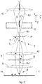
- FIG 1 is a highly schematic depiction of an embodiment of a CPM in which the present invention is implemented; more specifically, it shows an embodiment of a transmission-type microscope M, which, in this case, is a TEM/STEM (though, in the context of the current invention, it could just as validly be an ion-based microscope, for example).
- an electron source 2 such as a Schottky emitter, for example
- produces a beam (C/C') of electrons that traverse an electron-optical illuminator 4 serving to direct/focus them onto a chosen part of a specimen S (which may, for example, be (locally) thinned/planarized).
- This illuminator 4 has an electron-optical axis O, and will generally comprise a variety of electrostatic / magnetic lenses, (scan) deflector(s), correctors (such as stigmators), etc .; typically, it can also comprise a condenser system (the whole of item 4 is sometimes referred to as "a condenser system").
- the specimen S is held on a specimen holder H that can be positioned in multiple degrees of freedom by a positioning system / stage A; for example, the specimen holder H may comprise a finger that can be moved ( inter alia ) in the XY plane (see the depicted Cartesian coordinate system; typically, motion parallel to Z and (at least) tilt about X/Y will also be possible).
- a positioning system / stage A for example, the specimen holder H may comprise a finger that can be moved ( inter alia ) in the XY plane (see the depicted Cartesian coordinate system; typically, motion parallel to Z and (at least) tilt about X/Y will also be possible).
- Such movement allows different parts of the specimen S to be irradiated / imaged / inspected by the electron beam traveling along axis O (in the Z direction) (and/or allows scanning motion to be performed, as an alternative to beam scanning).
- a cooling device A' can be placed in intimate thermal contact with the specimen holder H, so as to maintain
- the (focused) electron beam C' traveling along axis O will interact with the specimen S in such a manner as to cause various types of "stimulated" radiation to emanate from the specimen S, including (for example) secondary electrons, backscattered electrons, X-rays and optical radiation (cathodoluminescence).
- various types of "stimulated” radiation including (for example) secondary electrons, backscattered electrons, X-rays and optical radiation (cathodoluminescence).
- one or more of these radiation types can be detected with the aid of analysis device 6, which might be a combined scintillator/photomultiplier or EDX (Energy-Dispersive X-Ray Spectroscopy) module, for instance; in such a case, an image could be constructed using basically the same principle as in a SEM.
- an imaging system combined objective/projection lens 8 which will generally comprise a variety of electrostatic / magnetic lenses, deflectors, correctors (such as stigmators), etc.
- this imaging system 8 can focus the transmitted electron flux onto a fluorescent screen 10, which, if desired, can be retracted/withdrawn (as schematically indicated by arrows 10') so as to get it out of the way of axis O.
- An image (or diffractogram) of (part of) the specimen S will be formed by imaging system 8 on screen 10, and this may be viewed through viewing port 12 located in a suitable part of a wall of enclosure V.
- the retraction mechanism for screen 10 may, for example, be mechanical and/or electrical in nature, and is not depicted here.
- controller E is connected to various illustrated components via control lines (buses) E'.
- This controller E can provide a variety of functions, such as synchronizing actions, providing setpoints, processing signals, performing calculations, and displaying messages/information on a display device (not depicted).
- the (schematically depicted) controller E may be (partially) inside or outside the enclosure V, and may have a unitary or composite structure, as desired.
- the interior of the enclosure V does not have to be kept at a strict vacuum; for example, in a so-called "Environmental TEM/STEM", a background atmosphere of a given gas is deliberately introduced/maintained within the enclosure V.
- FIG. 2 shows important aspects of Figure 1 in more detail.
- items D and P are positioned between condenser lens 41 and upper objective lens 42 (in many TEM designs, the last lens element of the illuminator 4 can be regarded as the first lens element of the projection system 8, so that the specimen S can be regarded as sitting partially within the projection system 8).
- the solid rays R S illustrate how the nominal/un-deflected beam gets collimated onto the specimen S, and focused onto the detector 14, and the dashed rays R D illustrate how the deflector D is imaged onto the detector 14, with an intermediate crossover R D '.
- Figure 3 shows a plan view of aperture plate P - which, in this specific case, comprises a rectilinear array of slit-shaped apertures extending substantially parallel to the X axis (the intended deflection/scan direction of beam C across the plate P). Two of these apertures P i and P j are labelled.
- the apertures may, for example, have a width in the range 12-20 ⁇ m, and extend (parallel to X) over a distance of ca.
- the beam segment C T is alternatingly interrupted (by the plate material between apertures) and transmitted (by successive apertures) so as to produce the pulse train T; for example, pulse T i in train T is produced by passage through aperture P i , and pulse T j in train T is produced by passage through aperture P j , etc.
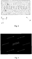
- Figure 4 this illustrates an example of a detection entity (in this case, a diffraction pattern) captured using an embodiment of the present invention. More specifically, the Figure shows the lowest orders of a Si [011] diffraction pattern - whereby the individual diffraction spots that would be obtained using a conventional technique are replaced by series (trains) of spatially displaced (temporally discriminated; positionally resolved) component spots. The arrow in the Figure indicates the direction of the beam deflection/scan (see Figures 2 , 3 ). Individual spots in each series have ⁇ 1 ps time resolution and are separated by ⁇ 10 ps steps.
Landscapes
- Chemical & Material Sciences (AREA)
- Analytical Chemistry (AREA)
- Analysing Materials By The Use Of Radiation (AREA)
Priority Applications (4)
| Application Number | Priority Date | Filing Date | Title |
|---|---|---|---|
| EP16157199.7A EP3133633B1 (en) | 2016-02-24 | 2016-02-24 | Studying dynamic specimen behavior in a charged-particle microscope |
| US15/389,151 US10340113B2 (en) | 2016-02-24 | 2016-12-22 | Studying dynamic specimen behavior in a charged-particle microscope |
| JP2017003750A JP6437020B2 (ja) | 2016-02-24 | 2017-01-13 | 荷電粒子顕微鏡を使用する方法及び荷電粒子顕微鏡 |
| CN201710041635.XA CN107123584B (zh) | 2016-02-24 | 2017-01-20 | 在带电粒子显微镜中研究动态样本行为 |
Applications Claiming Priority (1)
| Application Number | Priority Date | Filing Date | Title |
|---|---|---|---|
| EP16157199.7A EP3133633B1 (en) | 2016-02-24 | 2016-02-24 | Studying dynamic specimen behavior in a charged-particle microscope |
Publications (2)
| Publication Number | Publication Date |
|---|---|
| EP3133633A1 EP3133633A1 (en) | 2017-02-22 |
| EP3133633B1 true EP3133633B1 (en) | 2018-03-28 |
Family
ID=55411310
Family Applications (1)
| Application Number | Title | Priority Date | Filing Date |
|---|---|---|---|
| EP16157199.7A Active EP3133633B1 (en) | 2016-02-24 | 2016-02-24 | Studying dynamic specimen behavior in a charged-particle microscope |
Country Status (4)
| Country | Link |
|---|---|
| US (1) | US10340113B2 (https=) |
| EP (1) | EP3133633B1 (https=) |
| JP (1) | JP6437020B2 (https=) |
| CN (1) | CN107123584B (https=) |
Families Citing this family (17)
| Publication number | Priority date | Publication date | Assignee | Title |
|---|---|---|---|---|
| US10032599B2 (en) | 2016-11-28 | 2018-07-24 | FEI Cmnpany | Time-resolved charged particle microscopy |
| EP3327748B1 (en) | 2016-11-28 | 2019-03-27 | FEI Company | Time-of-flight charged particle spectroscopy |
| EP3444836B1 (en) * | 2017-08-17 | 2020-01-29 | FEI Company | Diffraction pattern detection in a transmission charged particle microscope |
| EP3534391B1 (en) * | 2018-03-01 | 2020-11-04 | FEI Company | Discriminative imaging technique in scanning transmission charged particle microscopy |
| EP3550585B1 (en) | 2018-04-05 | 2021-06-23 | FEI Company | Studying dynamic specimens in a transmission charged particle microscope |
| US10522323B2 (en) * | 2018-04-05 | 2019-12-31 | Fei Company | Electron energy loss spectroscopy with adjustable energy resolution |
| EP3564982A1 (en) * | 2018-05-02 | 2019-11-06 | FEI Company | Eels detection technique in an electron microscope |
| EP3591685A1 (en) * | 2018-07-06 | 2020-01-08 | FEI Company | Electron microscope with improved imaging resolution |
| US11114272B2 (en) * | 2019-09-25 | 2021-09-07 | Fei Company | Pulsed CFE electron source with fast blanker for ultrafast TEM applications |
| CN110890256B (zh) * | 2019-11-26 | 2021-07-27 | 华中科技大学 | 一种会聚角可调无磁飞秒电子源装置 |
| EP3869182A1 (en) * | 2020-02-19 | 2021-08-25 | FEI Company | Device and method for determining a property of a sample that is to be used in a charged particle microscope |
| EP3901982A1 (en) * | 2020-04-20 | 2021-10-27 | ASML Netherlands B.V. | An inspection tool, inspection tool operating method, and non-transitory computer readable medium |
| KR102790213B1 (ko) * | 2020-04-20 | 2025-04-03 | 에이에스엠엘 네델란즈 비.브이. | 검사 도구 및 검사 도구 작동 방법 |
| US11127562B1 (en) * | 2020-08-05 | 2021-09-21 | Fei Company | System and method for RF pulsed electron beam based STEM |
| EP3977937A1 (en) * | 2020-09-30 | 2022-04-06 | FEI Company | Method of investigating a specimen using a tomographic imaging apparatus |
| CN113984813B (zh) * | 2021-09-27 | 2024-07-26 | 上海大学 | 一种高通量薄膜晶体结构表征装置及方法 |
| JP7490832B2 (ja) | 2022-03-14 | 2024-05-27 | 日本電子株式会社 | 荷電粒子線装置および荷電粒子線装置の制御方法 |
Family Cites Families (18)
| Publication number | Priority date | Publication date | Assignee | Title |
|---|---|---|---|---|
| JPS4921829B1 (https=) * | 1969-05-16 | 1974-06-04 | ||
| JPS4937759Y1 (https=) * | 1970-12-18 | 1974-10-16 | ||
| JPS5538634B2 (https=) | 1972-06-24 | 1980-10-06 | ||
| JPS5115782B2 (https=) | 1972-08-17 | 1976-05-19 | ||
| US4445041A (en) * | 1981-06-02 | 1984-04-24 | Hewlett-Packard Company | Electron beam blanker |
| JPS60130031A (ja) | 1983-12-16 | 1985-07-11 | Toshiba Mach Co Ltd | パルスビ−ム発生装置 |
| US6414313B1 (en) * | 1999-06-01 | 2002-07-02 | Nikon Corporation | Multiple numerical aperture electron beam projection lithography system |
| CN100399014C (zh) | 2001-06-29 | 2008-07-02 | 中国科学院物理研究所 | 一种具有高时间分辨的电子显微镜 |
| US7557360B2 (en) * | 2003-10-16 | 2009-07-07 | Alis Corporation | Ion sources, systems and methods |
| JP2006196236A (ja) | 2005-01-12 | 2006-07-27 | Hitachi High-Technologies Corp | 電子顕微鏡及び観察方法 |
| US8569712B2 (en) * | 2010-10-07 | 2013-10-29 | Fei Company | Beam blanker for interrupting a beam of charged particles |
| JP5744629B2 (ja) * | 2011-06-03 | 2015-07-08 | 株式会社日立ハイテクノロジーズ | 電子顕微鏡及び電子線を用いた撮像方法 |
| EP2722865A1 (en) * | 2012-10-22 | 2014-04-23 | Fei Company | Beam pulsing device for use in charged-particle microscopy |
| US9867272B2 (en) * | 2012-10-17 | 2018-01-09 | Cornell University | Generation and acceleration of charged particles using compact devices and systems |
| US9165743B2 (en) * | 2014-02-14 | 2015-10-20 | Lawrence Livermore National Security, Llc | High-speed multiframe dynamic transmission electron microscope image acquisition system with arbitrary timing |
| US9464998B2 (en) * | 2014-06-20 | 2016-10-11 | California Institute Of Technology | Method and system for electron microscope with multiple cathodes |
| US9697982B2 (en) * | 2015-04-06 | 2017-07-04 | Euclid Techlabs, Llc | Apparatus for GHz rate high duty cycle pulsing and manipulation of low and medium energy DC electron beams |
| US10032599B2 (en) * | 2016-11-28 | 2018-07-24 | FEI Cmnpany | Time-resolved charged particle microscopy |
-
2016
- 2016-02-24 EP EP16157199.7A patent/EP3133633B1/en active Active
- 2016-12-22 US US15/389,151 patent/US10340113B2/en active Active
-
2017
- 2017-01-13 JP JP2017003750A patent/JP6437020B2/ja active Active
- 2017-01-20 CN CN201710041635.XA patent/CN107123584B/zh active Active
Non-Patent Citations (1)
| Title |
|---|
| None * |
Also Published As
| Publication number | Publication date |
|---|---|
| CN107123584A (zh) | 2017-09-01 |
| US10340113B2 (en) | 2019-07-02 |
| EP3133633A1 (en) | 2017-02-22 |
| US20170243713A1 (en) | 2017-08-24 |
| CN107123584B (zh) | 2019-03-19 |
| JP2017152366A (ja) | 2017-08-31 |
| JP6437020B2 (ja) | 2018-12-12 |
Similar Documents
| Publication | Publication Date | Title |
|---|---|---|
| EP3133633B1 (en) | Studying dynamic specimen behavior in a charged-particle microscope | |
| EP3340273B1 (en) | Time-resolved charged particle microscopy | |
| US9984852B1 (en) | Time-of-flight charged particle spectroscopy | |
| US9048060B2 (en) | Beam pulsing device for use in charged-particle microscopy | |
| CN109411320B (zh) | 透射带电粒子显微镜中的衍射图案检测 | |
| EP2993682A1 (en) | Method of performing spectroscopy in a transmission charged-particle microscope | |
| US10522323B2 (en) | Electron energy loss spectroscopy with adjustable energy resolution | |
| US10825648B2 (en) | Studying dynamic specimens in a transmission charged particle microscope | |
| JP2019194585A (ja) | 電子顕微鏡におけるeels検出技術 | |
| US11024483B2 (en) | Transmission charged particle microscope with adjustable beam energy spread | |
| US10559448B2 (en) | Transmission charged particle microscope with improved EELS/EFTEM module | |
| WO2025073497A1 (en) | Pulse compression for sample assessment |
Legal Events
| Date | Code | Title | Description |
|---|---|---|---|
| PUAI | Public reference made under article 153(3) epc to a published international application that has entered the european phase |
Free format text: ORIGINAL CODE: 0009012 |
|
| STAA | Information on the status of an ep patent application or granted ep patent |
Free format text: STATUS: REQUEST FOR EXAMINATION WAS MADE |
|
| 17P | Request for examination filed |
Effective date: 20161005 |
|
| AK | Designated contracting states |
Kind code of ref document: A1 Designated state(s): AL AT BE BG CH CY CZ DE DK EE ES FI FR GB GR HR HU IE IS IT LI LT LU LV MC MK MT NL NO PL PT RO RS SE SI SK SM TR |
|
| AX | Request for extension of the european patent |
Extension state: BA ME |
|
| GRAP | Despatch of communication of intention to grant a patent |
Free format text: ORIGINAL CODE: EPIDOSNIGR1 |
|
| STAA | Information on the status of an ep patent application or granted ep patent |
Free format text: STATUS: GRANT OF PATENT IS INTENDED |
|
| INTG | Intention to grant announced |
Effective date: 20171127 |
|
| GRAS | Grant fee paid |
Free format text: ORIGINAL CODE: EPIDOSNIGR3 |
|
| GRAA | (expected) grant |
Free format text: ORIGINAL CODE: 0009210 |
|
| STAA | Information on the status of an ep patent application or granted ep patent |
Free format text: STATUS: THE PATENT HAS BEEN GRANTED |
|
| AK | Designated contracting states |
Kind code of ref document: B1 Designated state(s): AL AT BE BG CH CY CZ DE DK EE ES FI FR GB GR HR HU IE IS IT LI LT LU LV MC MK MT NL NO PL PT RO RS SE SI SK SM TR |
|
| REG | Reference to a national code |
Ref country code: GB Ref legal event code: FG4D |
|
| REG | Reference to a national code |
Ref country code: CH Ref legal event code: EP |
|
| REG | Reference to a national code |
Ref country code: AT Ref legal event code: REF Ref document number: 984115 Country of ref document: AT Kind code of ref document: T Effective date: 20180415 |
|
| REG | Reference to a national code |
Ref country code: IE Ref legal event code: FG4D |
|
| REG | Reference to a national code |
Ref country code: DE Ref legal event code: R096 Ref document number: 602016002170 Country of ref document: DE |
|
| PG25 | Lapsed in a contracting state [announced via postgrant information from national office to epo] |
Ref country code: LT Free format text: LAPSE BECAUSE OF FAILURE TO SUBMIT A TRANSLATION OF THE DESCRIPTION OR TO PAY THE FEE WITHIN THE PRESCRIBED TIME-LIMIT Effective date: 20180328 Ref country code: FI Free format text: LAPSE BECAUSE OF FAILURE TO SUBMIT A TRANSLATION OF THE DESCRIPTION OR TO PAY THE FEE WITHIN THE PRESCRIBED TIME-LIMIT Effective date: 20180328 Ref country code: NO Free format text: LAPSE BECAUSE OF FAILURE TO SUBMIT A TRANSLATION OF THE DESCRIPTION OR TO PAY THE FEE WITHIN THE PRESCRIBED TIME-LIMIT Effective date: 20180628 Ref country code: HR Free format text: LAPSE BECAUSE OF FAILURE TO SUBMIT A TRANSLATION OF THE DESCRIPTION OR TO PAY THE FEE WITHIN THE PRESCRIBED TIME-LIMIT Effective date: 20180328 |
|
| REG | Reference to a national code |
Ref country code: NL Ref legal event code: MP Effective date: 20180328 |
|
| REG | Reference to a national code |
Ref country code: LT Ref legal event code: MG4D |
|
| PG25 | Lapsed in a contracting state [announced via postgrant information from national office to epo] |
Ref country code: LV Free format text: LAPSE BECAUSE OF FAILURE TO SUBMIT A TRANSLATION OF THE DESCRIPTION OR TO PAY THE FEE WITHIN THE PRESCRIBED TIME-LIMIT Effective date: 20180328 Ref country code: SE Free format text: LAPSE BECAUSE OF FAILURE TO SUBMIT A TRANSLATION OF THE DESCRIPTION OR TO PAY THE FEE WITHIN THE PRESCRIBED TIME-LIMIT Effective date: 20180328 Ref country code: RS Free format text: LAPSE BECAUSE OF FAILURE TO SUBMIT A TRANSLATION OF THE DESCRIPTION OR TO PAY THE FEE WITHIN THE PRESCRIBED TIME-LIMIT Effective date: 20180328 Ref country code: BG Free format text: LAPSE BECAUSE OF FAILURE TO SUBMIT A TRANSLATION OF THE DESCRIPTION OR TO PAY THE FEE WITHIN THE PRESCRIBED TIME-LIMIT Effective date: 20180628 Ref country code: GR Free format text: LAPSE BECAUSE OF FAILURE TO SUBMIT A TRANSLATION OF THE DESCRIPTION OR TO PAY THE FEE WITHIN THE PRESCRIBED TIME-LIMIT Effective date: 20180629 |
|
| PG25 | Lapsed in a contracting state [announced via postgrant information from national office to epo] |
Ref country code: RO Free format text: LAPSE BECAUSE OF FAILURE TO SUBMIT A TRANSLATION OF THE DESCRIPTION OR TO PAY THE FEE WITHIN THE PRESCRIBED TIME-LIMIT Effective date: 20180328 Ref country code: ES Free format text: LAPSE BECAUSE OF FAILURE TO SUBMIT A TRANSLATION OF THE DESCRIPTION OR TO PAY THE FEE WITHIN THE PRESCRIBED TIME-LIMIT Effective date: 20180328 Ref country code: NL Free format text: LAPSE BECAUSE OF FAILURE TO SUBMIT A TRANSLATION OF THE DESCRIPTION OR TO PAY THE FEE WITHIN THE PRESCRIBED TIME-LIMIT Effective date: 20180328 Ref country code: EE Free format text: LAPSE BECAUSE OF FAILURE TO SUBMIT A TRANSLATION OF THE DESCRIPTION OR TO PAY THE FEE WITHIN THE PRESCRIBED TIME-LIMIT Effective date: 20180328 Ref country code: PL Free format text: LAPSE BECAUSE OF FAILURE TO SUBMIT A TRANSLATION OF THE DESCRIPTION OR TO PAY THE FEE WITHIN THE PRESCRIBED TIME-LIMIT Effective date: 20180328 Ref country code: AL Free format text: LAPSE BECAUSE OF FAILURE TO SUBMIT A TRANSLATION OF THE DESCRIPTION OR TO PAY THE FEE WITHIN THE PRESCRIBED TIME-LIMIT Effective date: 20180328 |
|
| PG25 | Lapsed in a contracting state [announced via postgrant information from national office to epo] |
Ref country code: SM Free format text: LAPSE BECAUSE OF FAILURE TO SUBMIT A TRANSLATION OF THE DESCRIPTION OR TO PAY THE FEE WITHIN THE PRESCRIBED TIME-LIMIT Effective date: 20180328 Ref country code: SK Free format text: LAPSE BECAUSE OF FAILURE TO SUBMIT A TRANSLATION OF THE DESCRIPTION OR TO PAY THE FEE WITHIN THE PRESCRIBED TIME-LIMIT Effective date: 20180328 Ref country code: CZ Free format text: LAPSE BECAUSE OF FAILURE TO SUBMIT A TRANSLATION OF THE DESCRIPTION OR TO PAY THE FEE WITHIN THE PRESCRIBED TIME-LIMIT Effective date: 20180328 |
|
| REG | Reference to a national code |
Ref country code: AT Ref legal event code: MK05 Ref document number: 984115 Country of ref document: AT Kind code of ref document: T Effective date: 20180328 |
|
| PG25 | Lapsed in a contracting state [announced via postgrant information from national office to epo] |
Ref country code: PT Free format text: LAPSE BECAUSE OF FAILURE TO SUBMIT A TRANSLATION OF THE DESCRIPTION OR TO PAY THE FEE WITHIN THE PRESCRIBED TIME-LIMIT Effective date: 20180730 |
|
| REG | Reference to a national code |
Ref country code: DE Ref legal event code: R097 Ref document number: 602016002170 Country of ref document: DE |
|
| PG25 | Lapsed in a contracting state [announced via postgrant information from national office to epo] |
Ref country code: DK Free format text: LAPSE BECAUSE OF FAILURE TO SUBMIT A TRANSLATION OF THE DESCRIPTION OR TO PAY THE FEE WITHIN THE PRESCRIBED TIME-LIMIT Effective date: 20180328 Ref country code: AT Free format text: LAPSE BECAUSE OF FAILURE TO SUBMIT A TRANSLATION OF THE DESCRIPTION OR TO PAY THE FEE WITHIN THE PRESCRIBED TIME-LIMIT Effective date: 20180328 |
|
| PLBE | No opposition filed within time limit |
Free format text: ORIGINAL CODE: 0009261 |
|
| STAA | Information on the status of an ep patent application or granted ep patent |
Free format text: STATUS: NO OPPOSITION FILED WITHIN TIME LIMIT |
|
| PG25 | Lapsed in a contracting state [announced via postgrant information from national office to epo] |
Ref country code: IT Free format text: LAPSE BECAUSE OF FAILURE TO SUBMIT A TRANSLATION OF THE DESCRIPTION OR TO PAY THE FEE WITHIN THE PRESCRIBED TIME-LIMIT Effective date: 20180328 |
|
| 26N | No opposition filed |
Effective date: 20190103 |
|
| PG25 | Lapsed in a contracting state [announced via postgrant information from national office to epo] |
Ref country code: SI Free format text: LAPSE BECAUSE OF FAILURE TO SUBMIT A TRANSLATION OF THE DESCRIPTION OR TO PAY THE FEE WITHIN THE PRESCRIBED TIME-LIMIT Effective date: 20180328 |
|
| REG | Reference to a national code |
Ref country code: CH Ref legal event code: PL |
|
| PG25 | Lapsed in a contracting state [announced via postgrant information from national office to epo] |
Ref country code: LU Free format text: LAPSE BECAUSE OF NON-PAYMENT OF DUE FEES Effective date: 20190224 Ref country code: MC Free format text: LAPSE BECAUSE OF FAILURE TO SUBMIT A TRANSLATION OF THE DESCRIPTION OR TO PAY THE FEE WITHIN THE PRESCRIBED TIME-LIMIT Effective date: 20180328 |
|
| REG | Reference to a national code |
Ref country code: BE Ref legal event code: MM Effective date: 20190228 |
|
| REG | Reference to a national code |
Ref country code: IE Ref legal event code: MM4A |
|
| PG25 | Lapsed in a contracting state [announced via postgrant information from national office to epo] |
Ref country code: LI Free format text: LAPSE BECAUSE OF NON-PAYMENT OF DUE FEES Effective date: 20190228 Ref country code: CH Free format text: LAPSE BECAUSE OF NON-PAYMENT OF DUE FEES Effective date: 20190228 |
|
| PG25 | Lapsed in a contracting state [announced via postgrant information from national office to epo] |
Ref country code: IE Free format text: LAPSE BECAUSE OF NON-PAYMENT OF DUE FEES Effective date: 20190224 |
|
| PG25 | Lapsed in a contracting state [announced via postgrant information from national office to epo] |
Ref country code: FR Free format text: LAPSE BECAUSE OF NON-PAYMENT OF DUE FEES Effective date: 20190228 Ref country code: BE Free format text: LAPSE BECAUSE OF NON-PAYMENT OF DUE FEES Effective date: 20190228 |
|
| PG25 | Lapsed in a contracting state [announced via postgrant information from national office to epo] |
Ref country code: TR Free format text: LAPSE BECAUSE OF FAILURE TO SUBMIT A TRANSLATION OF THE DESCRIPTION OR TO PAY THE FEE WITHIN THE PRESCRIBED TIME-LIMIT Effective date: 20180328 |
|
| PG25 | Lapsed in a contracting state [announced via postgrant information from national office to epo] |
Ref country code: MT Free format text: LAPSE BECAUSE OF NON-PAYMENT OF DUE FEES Effective date: 20190224 |
|
| GBPC | Gb: european patent ceased through non-payment of renewal fee |
Effective date: 20200224 |
|
| PG25 | Lapsed in a contracting state [announced via postgrant information from national office to epo] |
Ref country code: GB Free format text: LAPSE BECAUSE OF NON-PAYMENT OF DUE FEES Effective date: 20200224 |
|
| PG25 | Lapsed in a contracting state [announced via postgrant information from national office to epo] |
Ref country code: CY Free format text: LAPSE BECAUSE OF FAILURE TO SUBMIT A TRANSLATION OF THE DESCRIPTION OR TO PAY THE FEE WITHIN THE PRESCRIBED TIME-LIMIT Effective date: 20180328 |
|
| PG25 | Lapsed in a contracting state [announced via postgrant information from national office to epo] |
Ref country code: IS Free format text: LAPSE BECAUSE OF FAILURE TO SUBMIT A TRANSLATION OF THE DESCRIPTION OR TO PAY THE FEE WITHIN THE PRESCRIBED TIME-LIMIT Effective date: 20180728 |
|
| PG25 | Lapsed in a contracting state [announced via postgrant information from national office to epo] |
Ref country code: HU Free format text: LAPSE BECAUSE OF FAILURE TO SUBMIT A TRANSLATION OF THE DESCRIPTION OR TO PAY THE FEE WITHIN THE PRESCRIBED TIME-LIMIT; INVALID AB INITIO Effective date: 20160224 |
|
| PG25 | Lapsed in a contracting state [announced via postgrant information from national office to epo] |
Ref country code: MK Free format text: LAPSE BECAUSE OF FAILURE TO SUBMIT A TRANSLATION OF THE DESCRIPTION OR TO PAY THE FEE WITHIN THE PRESCRIBED TIME-LIMIT Effective date: 20180328 |
|
| PGFP | Annual fee paid to national office [announced via postgrant information from national office to epo] |
Ref country code: DE Payment date: 20260113 Year of fee payment: 11 |