EP3133633B1 - Untersuchung des dynamischen probenverhaltens in einem teilchenstrahl-mikroskop - Google Patents
Untersuchung des dynamischen probenverhaltens in einem teilchenstrahl-mikroskop Download PDFInfo
- Publication number
- EP3133633B1 EP3133633B1 EP16157199.7A EP16157199A EP3133633B1 EP 3133633 B1 EP3133633 B1 EP 3133633B1 EP 16157199 A EP16157199 A EP 16157199A EP 3133633 B1 EP3133633 B1 EP 3133633B1
- Authority
- EP
- European Patent Office
- Prior art keywords
- specimen
- deflecting device
- pulses
- train
- array
- Prior art date
- Legal status (The legal status is an assumption and is not a legal conclusion. Google has not performed a legal analysis and makes no representation as to the accuracy of the status listed.)
- Active
Links
Images

Classifications
-
- H—ELECTRICITY
- H01—ELECTRIC ELEMENTS
- H01J—ELECTRIC DISCHARGE TUBES OR DISCHARGE LAMPS
- H01J37/00—Discharge tubes with provision for introducing objects or material to be exposed to the discharge, e.g. for the purpose of examination or processing thereof
- H01J37/26—Electron or ion microscopes; Electron or ion diffraction tubes
- H01J37/261—Details
-
- H—ELECTRICITY
- H01—ELECTRIC ELEMENTS
- H01J—ELECTRIC DISCHARGE TUBES OR DISCHARGE LAMPS
- H01J37/00—Discharge tubes with provision for introducing objects or material to be exposed to the discharge, e.g. for the purpose of examination or processing thereof
- H01J37/02—Details
- H01J37/04—Arrangements of electrodes and associated parts for generating or controlling the discharge, e.g. electron-optical arrangement or ion-optical arrangement
- H01J37/045—Beam blanking or chopping, i.e. arrangements for momentarily interrupting exposure to the discharge
-
- H—ELECTRICITY
- H01—ELECTRIC ELEMENTS
- H01J—ELECTRIC DISCHARGE TUBES OR DISCHARGE LAMPS
- H01J37/00—Discharge tubes with provision for introducing objects or material to be exposed to the discharge, e.g. for the purpose of examination or processing thereof
- H01J37/02—Details
- H01J37/04—Arrangements of electrodes and associated parts for generating or controlling the discharge, e.g. electron-optical arrangement or ion-optical arrangement
- H01J37/147—Arrangements for directing or deflecting the discharge along a desired path
- H01J37/1472—Deflecting along given lines
- H01J37/1474—Scanning means
-
- H—ELECTRICITY
- H01—ELECTRIC ELEMENTS
- H01J—ELECTRIC DISCHARGE TUBES OR DISCHARGE LAMPS
- H01J37/00—Discharge tubes with provision for introducing objects or material to be exposed to the discharge, e.g. for the purpose of examination or processing thereof
- H01J37/02—Details
- H01J37/20—Means for supporting or positioning the object or the material; Means for adjusting diaphragms or lenses associated with the support
-
- H—ELECTRICITY
- H01—ELECTRIC ELEMENTS
- H01J—ELECTRIC DISCHARGE TUBES OR DISCHARGE LAMPS
- H01J37/00—Discharge tubes with provision for introducing objects or material to be exposed to the discharge, e.g. for the purpose of examination or processing thereof
- H01J37/02—Details
- H01J37/244—Detectors; Associated components or circuits therefor
-
- H—ELECTRICITY
- H01—ELECTRIC ELEMENTS
- H01J—ELECTRIC DISCHARGE TUBES OR DISCHARGE LAMPS
- H01J37/00—Discharge tubes with provision for introducing objects or material to be exposed to the discharge, e.g. for the purpose of examination or processing thereof
- H01J37/26—Electron or ion microscopes; Electron or ion diffraction tubes
- H01J37/261—Details
- H01J37/265—Controlling the tube; circuit arrangements adapted to a particular application not otherwise provided, e.g. bright-field-dark-field illumination
-
- H—ELECTRICITY
- H01—ELECTRIC ELEMENTS
- H01J—ELECTRIC DISCHARGE TUBES OR DISCHARGE LAMPS
- H01J37/00—Discharge tubes with provision for introducing objects or material to be exposed to the discharge, e.g. for the purpose of examination or processing thereof
- H01J37/26—Electron or ion microscopes; Electron or ion diffraction tubes
- H01J37/266—Measurement of magnetic or electric fields in the object; Lorentzmicroscopy
-
- H—ELECTRICITY
- H01—ELECTRIC ELEMENTS
- H01J—ELECTRIC DISCHARGE TUBES OR DISCHARGE LAMPS
- H01J37/00—Discharge tubes with provision for introducing objects or material to be exposed to the discharge, e.g. for the purpose of examination or processing thereof
- H01J37/26—Electron or ion microscopes; Electron or ion diffraction tubes
- H01J37/28—Electron or ion microscopes; Electron or ion diffraction tubes with scanning beams
-
- H—ELECTRICITY
- H01—ELECTRIC ELEMENTS
- H01J—ELECTRIC DISCHARGE TUBES OR DISCHARGE LAMPS
- H01J2237/00—Discharge tubes exposing object to beam, e.g. for analysis treatment, etching, imaging
- H01J2237/04—Means for controlling the discharge
- H01J2237/043—Beam blanking
- H01J2237/0432—High speed and short duration
-
- H—ELECTRICITY
- H01—ELECTRIC ELEMENTS
- H01J—ELECTRIC DISCHARGE TUBES OR DISCHARGE LAMPS
- H01J2237/00—Discharge tubes exposing object to beam, e.g. for analysis treatment, etching, imaging
- H01J2237/04—Means for controlling the discharge
- H01J2237/043—Beam blanking
- H01J2237/0435—Multi-aperture
-
- H—ELECTRICITY
- H01—ELECTRIC ELEMENTS
- H01J—ELECTRIC DISCHARGE TUBES OR DISCHARGE LAMPS
- H01J2237/00—Discharge tubes exposing object to beam, e.g. for analysis treatment, etching, imaging
- H01J2237/15—Means for deflecting or directing discharge
- H01J2237/1504—Associated circuits
-
- H—ELECTRICITY
- H01—ELECTRIC ELEMENTS
- H01J—ELECTRIC DISCHARGE TUBES OR DISCHARGE LAMPS
- H01J2237/00—Discharge tubes exposing object to beam, e.g. for analysis treatment, etching, imaging
- H01J2237/244—Detection characterized by the detecting means
- H01J2237/2446—Position sensitive detectors
-
- H—ELECTRICITY
- H01—ELECTRIC ELEMENTS
- H01J—ELECTRIC DISCHARGE TUBES OR DISCHARGE LAMPS
- H01J2237/00—Discharge tubes exposing object to beam, e.g. for analysis treatment, etching, imaging
- H01J2237/244—Detection characterized by the detecting means
- H01J2237/24495—Signal processing, e.g. mixing of two or more signals
-
- H—ELECTRICITY
- H01—ELECTRIC ELEMENTS
- H01J—ELECTRIC DISCHARGE TUBES OR DISCHARGE LAMPS
- H01J2237/00—Discharge tubes exposing object to beam, e.g. for analysis treatment, etching, imaging
- H01J2237/245—Detection characterised by the variable being measured
- H01J2237/24571—Measurements of non-electric or non-magnetic variables
- H01J2237/24585—Other variables, e.g. energy, mass, velocity, time, temperature
-
- H—ELECTRICITY
- H01—ELECTRIC ELEMENTS
- H01J—ELECTRIC DISCHARGE TUBES OR DISCHARGE LAMPS
- H01J2237/00—Discharge tubes exposing object to beam, e.g. for analysis treatment, etching, imaging
- H01J2237/26—Electron or ion microscopes
- H01J2237/28—Scanning microscopes
- H01J2237/2802—Transmission microscopes
Definitions
- the invention relates to a method of using a Charged Particle Microscope, comprising:
- Charged particle microscopy is a well-known and increasingly important technique for imaging microscopic objects, particularly in the form of electron microscopy.
- the basic genus of electron microscope has undergone evolution into a number of well-known apparatus species, such as the Transmission Electron Microscope (TEM), Scanning Electron Microscope (SEM), and Scanning Transmission Electron Microscope (STEM), and also into various sub-species, such as so-called “dual-beam” tools (e.g. a FIB-SEM), which additionally employ a "machining" Focused Ion Beam (FIB), allowing supportive activities such as ion-beam milling or lon-Beam-Induced Deposition (IBID), for example. More specifically:
- charged particle microscopy can also be performed using other species of charged particle.
- charged particle should be broadly interpreted as encompassing electrons, positive ions (e.g . Ga or He ions), negative ions, protons and positrons, for instance.
- positive ions e.g . Ga or He ions
- negative ions e.g . Ga or He ions
- protons e.g., protons
- positrons positrons
- a charged particle microscope may also have other functionalities, such as performing spectroscopy, examining diffractograms, etc .
- a Charged Particle Microscope will comprise at least the following components:
- the CPM will also comprise:
- the invention may - by way of example - sometimes be set forth in the specific context of electron microscopy; however, such simplification is intended solely for clarity/illustrative purposes, and should not be interpreted as limiting.
- An analogy can be made here to photography, where an extended exposure is perfectly suitable for capturing a static scene (such as in astronomy), but is intrinsically unsuited to capturing a dynamic scene (such as a high-speed impact, for example); in this latter case, one will have to resort to using a short shutter time and/or a short flash duration (as in the case of stroboscopic photography).
- "dynamic" specimens as referred to here are not necessarily moving; more generically formulated, they are "evolving”, e.g. in the sense that they are undergoing a rapid phase transition, chemical reaction, transmutation, etc.
- CPMs are highly versatile tools, because they have imaging, diffractometric and spectroscopic functionality; however, to date, they do not offer many (satisfactory) ways of analyzing dynamic specimens, particularly on extremely short (e.g. picosecond) timescales.
- an external stimulus can be applied to the specimen while (and/or just before) it is being irradiated with the inventive pulse train.
- a stimulus might, for example, comprise application of an electrical signal, irradiation with a photon (or other particle) beam, administration of a chemical reagent, etc. This may, for example, be done so as to precipitate and/or influence particular dynamic behavior in the specimen.
- the invention employs a deflecting device comprising a resonant RF (radio frequency) cavity through which the beam passes.
- RF radio frequency
- the beam upstream of / entering the deflecting device (the "entrant beam”) is pulsed.
- Pulsing the entrant beam in this manner has a number of advantages. For example, if the employed deflecting device has a "characteristic frequency" of deflection (as in the case of the resonance frequency of an RF resonant cavity), then using a pulsed entrant beam allows the ultimate (effective) deflection frequency of the beam leaving the deflecting device (the "emergent beam”) to be adjusted (reduced).
- this effect can be understood in terms of the superposition of two signals of different frequency - which produces so-called "beats" at a frequency lower than the frequency of either of the superimposed beams; more generally, however, the entrant beam can be pulsed at the desired frequency of the emergent beam, and synchronized (phase-locked) to the driving (RF) frequency used to excite the deflecting device.
- the characteristic frequency is considered to be undesirably high for a given application (e.g. ⁇ 3x10 9 Hz, as produced by a given RF cavity configuration)
- the present embodiment allows a lower (ultimate) deflection frequency to be selected, if desired (e.g. ⁇ 10 6 -10 4 Hz).
- a pulsed entrant beam can typically have a larger instantaneous beam current than a continuous entrant beam, resulting in more charged particles (on average) in each of the pulses of the pulse train, with an attendant increase in signal-to-noise ratio.
- a pulsed entrant beam as referred to here can, for example, be realized by using a pulsed laser to excite/trigger/modulate a photoelectric source [or to modulate the thermal excitation of a thermal source (such as an LaB 6 (hot cathode) crystal) or a thermionic source (such as a Schottky emitter), for instance].
- a thermal source such as an LaB 6 (hot cathode) crystal
- a thermionic source such as a Schottky emitter
- an oscillatory beam blanker/chopper can be used somewhere between the source and deflecting device.
- the array of apertures in the plate can extend in a straight line, but may alternatively lie along a curved line, if desired.
- a given plate may contain several different aperture arrays, e.g. with different array pitches and/or different aperture sizes/shapes and/or extending in different directions.
- the separation of neighboring apertures in an array does not have to be constant, and may instead vary, if desired ( e.g. to compensate for higher-order effects associated with the beam deflection across the array).
- the shape/size of the apertures is also a matter of choice, whereby it deserves mention that the shape/size of an aperture parallel to the direction of beam deflection/scan is generally more important than the shape/size of that aperture perpendicular to said direction; so, for example, the apertures could be round, or slit-shaped, as desired.
- the apertures will have a width (parallel to the beam deflection/scan direction) in the range 0.5-20 ⁇ m, and a mutual separation (in the same direction) in the range 10-200 ⁇ m, although such values are, of course, non-limiting.
- FIG 1 is a highly schematic depiction of an embodiment of a CPM in which the present invention is implemented; more specifically, it shows an embodiment of a transmission-type microscope M, which, in this case, is a TEM/STEM (though, in the context of the current invention, it could just as validly be an ion-based microscope, for example).
- an electron source 2 such as a Schottky emitter, for example
- produces a beam (C/C') of electrons that traverse an electron-optical illuminator 4 serving to direct/focus them onto a chosen part of a specimen S (which may, for example, be (locally) thinned/planarized).
- This illuminator 4 has an electron-optical axis O, and will generally comprise a variety of electrostatic / magnetic lenses, (scan) deflector(s), correctors (such as stigmators), etc .; typically, it can also comprise a condenser system (the whole of item 4 is sometimes referred to as "a condenser system").
- the specimen S is held on a specimen holder H that can be positioned in multiple degrees of freedom by a positioning system / stage A; for example, the specimen holder H may comprise a finger that can be moved ( inter alia ) in the XY plane (see the depicted Cartesian coordinate system; typically, motion parallel to Z and (at least) tilt about X/Y will also be possible).
- a positioning system / stage A for example, the specimen holder H may comprise a finger that can be moved ( inter alia ) in the XY plane (see the depicted Cartesian coordinate system; typically, motion parallel to Z and (at least) tilt about X/Y will also be possible).
- Such movement allows different parts of the specimen S to be irradiated / imaged / inspected by the electron beam traveling along axis O (in the Z direction) (and/or allows scanning motion to be performed, as an alternative to beam scanning).
- a cooling device A' can be placed in intimate thermal contact with the specimen holder H, so as to maintain
- the (focused) electron beam C' traveling along axis O will interact with the specimen S in such a manner as to cause various types of "stimulated" radiation to emanate from the specimen S, including (for example) secondary electrons, backscattered electrons, X-rays and optical radiation (cathodoluminescence).
- various types of "stimulated” radiation including (for example) secondary electrons, backscattered electrons, X-rays and optical radiation (cathodoluminescence).
- one or more of these radiation types can be detected with the aid of analysis device 6, which might be a combined scintillator/photomultiplier or EDX (Energy-Dispersive X-Ray Spectroscopy) module, for instance; in such a case, an image could be constructed using basically the same principle as in a SEM.
- an imaging system combined objective/projection lens 8 which will generally comprise a variety of electrostatic / magnetic lenses, deflectors, correctors (such as stigmators), etc.
- this imaging system 8 can focus the transmitted electron flux onto a fluorescent screen 10, which, if desired, can be retracted/withdrawn (as schematically indicated by arrows 10') so as to get it out of the way of axis O.
- An image (or diffractogram) of (part of) the specimen S will be formed by imaging system 8 on screen 10, and this may be viewed through viewing port 12 located in a suitable part of a wall of enclosure V.
- the retraction mechanism for screen 10 may, for example, be mechanical and/or electrical in nature, and is not depicted here.
- controller E is connected to various illustrated components via control lines (buses) E'.
- This controller E can provide a variety of functions, such as synchronizing actions, providing setpoints, processing signals, performing calculations, and displaying messages/information on a display device (not depicted).
- the (schematically depicted) controller E may be (partially) inside or outside the enclosure V, and may have a unitary or composite structure, as desired.
- the interior of the enclosure V does not have to be kept at a strict vacuum; for example, in a so-called "Environmental TEM/STEM", a background atmosphere of a given gas is deliberately introduced/maintained within the enclosure V.
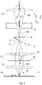
- FIG. 2 shows important aspects of Figure 1 in more detail.
- items D and P are positioned between condenser lens 41 and upper objective lens 42 (in many TEM designs, the last lens element of the illuminator 4 can be regarded as the first lens element of the projection system 8, so that the specimen S can be regarded as sitting partially within the projection system 8).
- the solid rays R S illustrate how the nominal/un-deflected beam gets collimated onto the specimen S, and focused onto the detector 14, and the dashed rays R D illustrate how the deflector D is imaged onto the detector 14, with an intermediate crossover R D '.
- Figure 3 shows a plan view of aperture plate P - which, in this specific case, comprises a rectilinear array of slit-shaped apertures extending substantially parallel to the X axis (the intended deflection/scan direction of beam C across the plate P). Two of these apertures P i and P j are labelled.
- the apertures may, for example, have a width in the range 12-20 ⁇ m, and extend (parallel to X) over a distance of ca.
- the beam segment C T is alternatingly interrupted (by the plate material between apertures) and transmitted (by successive apertures) so as to produce the pulse train T; for example, pulse T i in train T is produced by passage through aperture P i , and pulse T j in train T is produced by passage through aperture P j , etc.
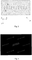
- Figure 4 this illustrates an example of a detection entity (in this case, a diffraction pattern) captured using an embodiment of the present invention. More specifically, the Figure shows the lowest orders of a Si [011] diffraction pattern - whereby the individual diffraction spots that would be obtained using a conventional technique are replaced by series (trains) of spatially displaced (temporally discriminated; positionally resolved) component spots. The arrow in the Figure indicates the direction of the beam deflection/scan (see Figures 2 , 3 ). Individual spots in each series have ⁇ 1 ps time resolution and are separated by ⁇ 10 ps steps.
Landscapes
- Chemical & Material Sciences (AREA)
- Analytical Chemistry (AREA)
- Analysing Materials By The Use Of Radiation (AREA)
Claims (8)
- Verfahren zur Verwendung eines Geladene-Teilchenstrahlmikroskops, das aufweist;- eine Probenhalterung zum Halten einer Probe;- eine Quelle zum Erzeugen eines Bestrahlungsstrahls aus geladenen Teilchen;- eine Beleuchtungseinrichtung zum Leiten des Strahls, um die Probe zu bestrahlen;- eine Erfassungseinrichtung zum Erfassen eines Flusses einer austretenden Strahlung, die aus der Probe stammt, ansprechend auf die Bestrahlung,wobei das Verfahren aufweist:- Bestrahlen der Probe mit einem Pulszug und Verwenden der Erfassungseinrichtung, um eine positionsaufgelöste Erfassung der begleitenden austretenden Strahlung durchzuführen,gekennzeichnet durch die folgenden Schritte:- in der Beleuchtungseinrichtung Bereitstellen einer Lochblende, die eine Anordnung von Öffnungen aufweist;- Bereitstellen einer Ablenkungsvorrichtung, die einen RF-Resonanzhohlraum aufweist, welchen der Strahl durchläuft, und Verwenden der Ablenkungsvorrichtung, um den Strahl quer zu der Anordnung abzutasten zu lassen, wodurch der Strahl abwechselnd unterbrochen und transmittiert wird, um den Zug von Strahlpulsen zu erzeugen.
- Verfahren nach Anspruch 1, wobei der Hohlraum in der TM110-Mode angeregt wird.
- Verfahren nach einem der Ansprüche 1 - 2, wobei der Strahl vor dem Eintritt in die Ablenkvorrichtung gepulst wird.
- Verfahren nach einem der Ansprüche 1 - 3, wobei eine Ebene der Ablenkvorrichtung auf eine Ebene der Probe abgebildet wird.
- Verfahren nach einem der Ansprüche 1 - 4, wobei die Lochblende an einem Zwischenstrahlkreuzungspunkt zwischen der Ablenkvorrichtung und der Probe angeordnet ist.
- Verfahren nach einem der Ansprüche 1 - 5, wobei aufeinanderfolgende Pulse in dem Pulszug eine Trennung im Bereich von 1 - 100 Pikosekunden haben.
- Verfahren nach einem der Ansprüche 1 bis 6, wobei die Erfassungseinrichtung verwendet wird, um eine zeitaufgelöste Reihe von Beugungsmustern, die von der Probe erzeugt werden, zu registrieren.
- Geladene-Teilchenstrahlmikroskop, das aufweist:- eine Probenhalterung zum Halten einer Probe;- eine Quelle zum Erzeugen eines Bestrahlungsstrahls aus geladenen Teilchen;- eine Beleuchtungseinrichtung zum Richten des Strahls, um die Probe zu bestrahlen;- eine Erfassungseinrichtung zum Erfassen eines Flusses einer austretenden Strahlung, die aus der Probe stammt, ansprechend auf die Bestrahlung;- eine elektronische Steuerung zum Steuern von Aspekten des Betriebs des Mikroskops, wobei die elektronische Steuerung aufgebaut ist, um eine positionsaufgelöste Erfassung der aus der Probe austretenden Strahlung durchzuführen, wenn die Probe mit einem Pulszug bestrahlt wird,dadurch gekennzeichnet, dass das Mikroskop ferner aufweist:- eine Strahlablenkungsvorrichtung, die einen RF-Resonanzhohlraum aufweist, durch den der Strahl geleitet wird;- eine Lochblende, die eine Anordnung von Öffnungen aufweist, die in der Beleuchtungseinrichtung angeordnet ist,und dass die elektronische Steuerung aufgebaut ist, um:- die Ablenkungsvorrichtung anzutreiben, um den Strahl quer zu der Anordnung abtasten zu lassen, wodurch der Strahl abwechselnd unterbrochen und transmittiert wird, um den Zug von Strahlpulsen zu erzeugen.
Priority Applications (4)
| Application Number | Priority Date | Filing Date | Title |
|---|---|---|---|
| EP16157199.7A EP3133633B1 (de) | 2016-02-24 | 2016-02-24 | Untersuchung des dynamischen probenverhaltens in einem teilchenstrahl-mikroskop |
| US15/389,151 US10340113B2 (en) | 2016-02-24 | 2016-12-22 | Studying dynamic specimen behavior in a charged-particle microscope |
| JP2017003750A JP6437020B2 (ja) | 2016-02-24 | 2017-01-13 | 荷電粒子顕微鏡を使用する方法及び荷電粒子顕微鏡 |
| CN201710041635.XA CN107123584B (zh) | 2016-02-24 | 2017-01-20 | 在带电粒子显微镜中研究动态样本行为 |
Applications Claiming Priority (1)
| Application Number | Priority Date | Filing Date | Title |
|---|---|---|---|
| EP16157199.7A EP3133633B1 (de) | 2016-02-24 | 2016-02-24 | Untersuchung des dynamischen probenverhaltens in einem teilchenstrahl-mikroskop |
Publications (2)
| Publication Number | Publication Date |
|---|---|
| EP3133633A1 EP3133633A1 (de) | 2017-02-22 |
| EP3133633B1 true EP3133633B1 (de) | 2018-03-28 |
Family
ID=55411310
Family Applications (1)
| Application Number | Title | Priority Date | Filing Date |
|---|---|---|---|
| EP16157199.7A Active EP3133633B1 (de) | 2016-02-24 | 2016-02-24 | Untersuchung des dynamischen probenverhaltens in einem teilchenstrahl-mikroskop |
Country Status (4)
| Country | Link |
|---|---|
| US (1) | US10340113B2 (de) |
| EP (1) | EP3133633B1 (de) |
| JP (1) | JP6437020B2 (de) |
| CN (1) | CN107123584B (de) |
Families Citing this family (17)
| Publication number | Priority date | Publication date | Assignee | Title |
|---|---|---|---|---|
| EP3327748B1 (de) | 2016-11-28 | 2019-03-27 | FEI Company | Flugzeitspektroskopie geladener teilchen |
| US10032599B2 (en) | 2016-11-28 | 2018-07-24 | FEI Cmnpany | Time-resolved charged particle microscopy |
| EP3444836B1 (de) * | 2017-08-17 | 2020-01-29 | FEI Company | Beugungsbilddetektion in einem ladungsträgerteilchenmikroskop |
| EP3534391B1 (de) * | 2018-03-01 | 2020-11-04 | FEI Company | Charakterisierende abbildungstechnik in der rastertransmissionsladungsteilchenmikroskopie |
| US10522323B2 (en) * | 2018-04-05 | 2019-12-31 | Fei Company | Electron energy loss spectroscopy with adjustable energy resolution |
| EP3550585B1 (de) | 2018-04-05 | 2021-06-23 | FEI Company | Untersuchung dynamischer proben in einem transmissionsteilchenmikroskop |
| EP3564982A1 (de) * | 2018-05-02 | 2019-11-06 | FEI Company | Technik zur eels-detektion in einem elektronenmikroskop |
| EP3591685A1 (de) * | 2018-07-06 | 2020-01-08 | FEI Company | Elektronenmikroskop mit verbesserter abbildungsauflösung |
| US11114272B2 (en) * | 2019-09-25 | 2021-09-07 | Fei Company | Pulsed CFE electron source with fast blanker for ultrafast TEM applications |
| CN110890256B (zh) * | 2019-11-26 | 2021-07-27 | 华中科技大学 | 一种会聚角可调无磁飞秒电子源装置 |
| EP3869182A1 (de) * | 2020-02-19 | 2021-08-25 | FEI Company | Vorrichtung und verfahren zur bestimmung einer eigenschaft einer probe, die in einem mikroskop für geladene teilchen verwendet werden soll |
| EP3901982A1 (de) * | 2020-04-20 | 2021-10-27 | ASML Netherlands B.V. | Inspektionswerkzeug, verfahren zum betreiben eines inspektionswerkzeugs und nichttransitorisches computerlesbares medium |
| KR102790213B1 (ko) * | 2020-04-20 | 2025-04-03 | 에이에스엠엘 네델란즈 비.브이. | 검사 도구 및 검사 도구 작동 방법 |
| US11127562B1 (en) * | 2020-08-05 | 2021-09-21 | Fei Company | System and method for RF pulsed electron beam based STEM |
| EP3977937B1 (de) * | 2020-09-30 | 2026-07-01 | FEI Company | Verfahren zur untersuchung einer probe unter verwendung einer tomographischen bilderzeugungsvorrichtung |
| CN113984813B (zh) * | 2021-09-27 | 2024-07-26 | 上海大学 | 一种高通量薄膜晶体结构表征装置及方法 |
| JP7490832B2 (ja) | 2022-03-14 | 2024-05-27 | 日本電子株式会社 | 荷電粒子線装置および荷電粒子線装置の制御方法 |
Family Cites Families (18)
| Publication number | Priority date | Publication date | Assignee | Title |
|---|---|---|---|---|
| JPS4921829B1 (de) * | 1969-05-16 | 1974-06-04 | ||
| JPS4937759Y1 (de) * | 1970-12-18 | 1974-10-16 | ||
| JPS5538634B2 (de) | 1972-06-24 | 1980-10-06 | ||
| JPS5115782B2 (de) | 1972-08-17 | 1976-05-19 | ||
| US4445041A (en) * | 1981-06-02 | 1984-04-24 | Hewlett-Packard Company | Electron beam blanker |
| JPS60130031A (ja) | 1983-12-16 | 1985-07-11 | Toshiba Mach Co Ltd | パルスビ−ム発生装置 |
| US6414313B1 (en) * | 1999-06-01 | 2002-07-02 | Nikon Corporation | Multiple numerical aperture electron beam projection lithography system |
| CN100399014C (zh) | 2001-06-29 | 2008-07-02 | 中国科学院物理研究所 | 一种具有高时间分辨的电子显微镜 |
| US7557360B2 (en) * | 2003-10-16 | 2009-07-07 | Alis Corporation | Ion sources, systems and methods |
| JP2006196236A (ja) | 2005-01-12 | 2006-07-27 | Hitachi High-Technologies Corp | 電子顕微鏡及び観察方法 |
| US8569712B2 (en) * | 2010-10-07 | 2013-10-29 | Fei Company | Beam blanker for interrupting a beam of charged particles |
| JP5744629B2 (ja) * | 2011-06-03 | 2015-07-08 | 株式会社日立ハイテクノロジーズ | 電子顕微鏡及び電子線を用いた撮像方法 |
| WO2014123591A2 (en) * | 2012-10-17 | 2014-08-14 | Cornell University | Generation and acceleration of charged particles using compact devices and systems |
| EP2722865A1 (de) | 2012-10-22 | 2014-04-23 | Fei Company | Strahlpuls-Erzeuger zur Verwendung in der Teilchenstrahlmikroskopie |
| US9165743B2 (en) * | 2014-02-14 | 2015-10-20 | Lawrence Livermore National Security, Llc | High-speed multiframe dynamic transmission electron microscope image acquisition system with arbitrary timing |
| US9464998B2 (en) * | 2014-06-20 | 2016-10-11 | California Institute Of Technology | Method and system for electron microscope with multiple cathodes |
| US9697982B2 (en) * | 2015-04-06 | 2017-07-04 | Euclid Techlabs, Llc | Apparatus for GHz rate high duty cycle pulsing and manipulation of low and medium energy DC electron beams |
| US10032599B2 (en) * | 2016-11-28 | 2018-07-24 | FEI Cmnpany | Time-resolved charged particle microscopy |
-
2016
- 2016-02-24 EP EP16157199.7A patent/EP3133633B1/de active Active
- 2016-12-22 US US15/389,151 patent/US10340113B2/en active Active
-
2017
- 2017-01-13 JP JP2017003750A patent/JP6437020B2/ja active Active
- 2017-01-20 CN CN201710041635.XA patent/CN107123584B/zh active Active
Non-Patent Citations (1)
| Title |
|---|
| None * |
Also Published As
| Publication number | Publication date |
|---|---|
| CN107123584B (zh) | 2019-03-19 |
| US10340113B2 (en) | 2019-07-02 |
| JP2017152366A (ja) | 2017-08-31 |
| EP3133633A1 (de) | 2017-02-22 |
| JP6437020B2 (ja) | 2018-12-12 |
| US20170243713A1 (en) | 2017-08-24 |
| CN107123584A (zh) | 2017-09-01 |
Similar Documents
| Publication | Publication Date | Title |
|---|---|---|
| US10340113B2 (en) | Studying dynamic specimen behavior in a charged-particle microscope | |
| EP3340273B1 (de) | Zeitaufgelöste ladungsträgerteilchenspektroskopie | |
| US9048060B2 (en) | Beam pulsing device for use in charged-particle microscopy | |
| US9984852B1 (en) | Time-of-flight charged particle spectroscopy | |
| CN109411320B (zh) | 透射带电粒子显微镜中的衍射图案检测 | |
| EP2993682A1 (de) | Verfahren zur Spektroskopiedurchführung in einem Transmissions-Ladungsträger-Mikroskop | |
| US10522323B2 (en) | Electron energy loss spectroscopy with adjustable energy resolution | |
| JP2019194585A (ja) | 電子顕微鏡におけるeels検出技術 | |
| US10825648B2 (en) | Studying dynamic specimens in a transmission charged particle microscope | |
| US11024483B2 (en) | Transmission charged particle microscope with adjustable beam energy spread | |
| US10559448B2 (en) | Transmission charged particle microscope with improved EELS/EFTEM module | |
| WO2025073497A1 (en) | Pulse compression for sample assessment |
Legal Events
| Date | Code | Title | Description |
|---|---|---|---|
| PUAI | Public reference made under article 153(3) epc to a published international application that has entered the european phase |
Free format text: ORIGINAL CODE: 0009012 |
|
| STAA | Information on the status of an ep patent application or granted ep patent |
Free format text: STATUS: REQUEST FOR EXAMINATION WAS MADE |
|
| 17P | Request for examination filed |
Effective date: 20161005 |
|
| AK | Designated contracting states |
Kind code of ref document: A1 Designated state(s): AL AT BE BG CH CY CZ DE DK EE ES FI FR GB GR HR HU IE IS IT LI LT LU LV MC MK MT NL NO PL PT RO RS SE SI SK SM TR |
|
| AX | Request for extension of the european patent |
Extension state: BA ME |
|
| GRAP | Despatch of communication of intention to grant a patent |
Free format text: ORIGINAL CODE: EPIDOSNIGR1 |
|
| STAA | Information on the status of an ep patent application or granted ep patent |
Free format text: STATUS: GRANT OF PATENT IS INTENDED |
|
| INTG | Intention to grant announced |
Effective date: 20171127 |
|
| GRAS | Grant fee paid |
Free format text: ORIGINAL CODE: EPIDOSNIGR3 |
|
| GRAA | (expected) grant |
Free format text: ORIGINAL CODE: 0009210 |
|
| STAA | Information on the status of an ep patent application or granted ep patent |
Free format text: STATUS: THE PATENT HAS BEEN GRANTED |
|
| AK | Designated contracting states |
Kind code of ref document: B1 Designated state(s): AL AT BE BG CH CY CZ DE DK EE ES FI FR GB GR HR HU IE IS IT LI LT LU LV MC MK MT NL NO PL PT RO RS SE SI SK SM TR |
|
| REG | Reference to a national code |
Ref country code: GB Ref legal event code: FG4D |
|
| REG | Reference to a national code |
Ref country code: CH Ref legal event code: EP |
|
| REG | Reference to a national code |
Ref country code: AT Ref legal event code: REF Ref document number: 984115 Country of ref document: AT Kind code of ref document: T Effective date: 20180415 |
|
| REG | Reference to a national code |
Ref country code: IE Ref legal event code: FG4D |
|
| REG | Reference to a national code |
Ref country code: DE Ref legal event code: R096 Ref document number: 602016002170 Country of ref document: DE |
|
| PG25 | Lapsed in a contracting state [announced via postgrant information from national office to epo] |
Ref country code: LT Free format text: LAPSE BECAUSE OF FAILURE TO SUBMIT A TRANSLATION OF THE DESCRIPTION OR TO PAY THE FEE WITHIN THE PRESCRIBED TIME-LIMIT Effective date: 20180328 Ref country code: FI Free format text: LAPSE BECAUSE OF FAILURE TO SUBMIT A TRANSLATION OF THE DESCRIPTION OR TO PAY THE FEE WITHIN THE PRESCRIBED TIME-LIMIT Effective date: 20180328 Ref country code: NO Free format text: LAPSE BECAUSE OF FAILURE TO SUBMIT A TRANSLATION OF THE DESCRIPTION OR TO PAY THE FEE WITHIN THE PRESCRIBED TIME-LIMIT Effective date: 20180628 Ref country code: HR Free format text: LAPSE BECAUSE OF FAILURE TO SUBMIT A TRANSLATION OF THE DESCRIPTION OR TO PAY THE FEE WITHIN THE PRESCRIBED TIME-LIMIT Effective date: 20180328 |
|
| REG | Reference to a national code |
Ref country code: NL Ref legal event code: MP Effective date: 20180328 |
|
| REG | Reference to a national code |
Ref country code: LT Ref legal event code: MG4D |
|
| PG25 | Lapsed in a contracting state [announced via postgrant information from national office to epo] |
Ref country code: LV Free format text: LAPSE BECAUSE OF FAILURE TO SUBMIT A TRANSLATION OF THE DESCRIPTION OR TO PAY THE FEE WITHIN THE PRESCRIBED TIME-LIMIT Effective date: 20180328 Ref country code: SE Free format text: LAPSE BECAUSE OF FAILURE TO SUBMIT A TRANSLATION OF THE DESCRIPTION OR TO PAY THE FEE WITHIN THE PRESCRIBED TIME-LIMIT Effective date: 20180328 Ref country code: RS Free format text: LAPSE BECAUSE OF FAILURE TO SUBMIT A TRANSLATION OF THE DESCRIPTION OR TO PAY THE FEE WITHIN THE PRESCRIBED TIME-LIMIT Effective date: 20180328 Ref country code: BG Free format text: LAPSE BECAUSE OF FAILURE TO SUBMIT A TRANSLATION OF THE DESCRIPTION OR TO PAY THE FEE WITHIN THE PRESCRIBED TIME-LIMIT Effective date: 20180628 Ref country code: GR Free format text: LAPSE BECAUSE OF FAILURE TO SUBMIT A TRANSLATION OF THE DESCRIPTION OR TO PAY THE FEE WITHIN THE PRESCRIBED TIME-LIMIT Effective date: 20180629 |
|
| PG25 | Lapsed in a contracting state [announced via postgrant information from national office to epo] |
Ref country code: RO Free format text: LAPSE BECAUSE OF FAILURE TO SUBMIT A TRANSLATION OF THE DESCRIPTION OR TO PAY THE FEE WITHIN THE PRESCRIBED TIME-LIMIT Effective date: 20180328 Ref country code: ES Free format text: LAPSE BECAUSE OF FAILURE TO SUBMIT A TRANSLATION OF THE DESCRIPTION OR TO PAY THE FEE WITHIN THE PRESCRIBED TIME-LIMIT Effective date: 20180328 Ref country code: NL Free format text: LAPSE BECAUSE OF FAILURE TO SUBMIT A TRANSLATION OF THE DESCRIPTION OR TO PAY THE FEE WITHIN THE PRESCRIBED TIME-LIMIT Effective date: 20180328 Ref country code: EE Free format text: LAPSE BECAUSE OF FAILURE TO SUBMIT A TRANSLATION OF THE DESCRIPTION OR TO PAY THE FEE WITHIN THE PRESCRIBED TIME-LIMIT Effective date: 20180328 Ref country code: PL Free format text: LAPSE BECAUSE OF FAILURE TO SUBMIT A TRANSLATION OF THE DESCRIPTION OR TO PAY THE FEE WITHIN THE PRESCRIBED TIME-LIMIT Effective date: 20180328 Ref country code: AL Free format text: LAPSE BECAUSE OF FAILURE TO SUBMIT A TRANSLATION OF THE DESCRIPTION OR TO PAY THE FEE WITHIN THE PRESCRIBED TIME-LIMIT Effective date: 20180328 |
|
| PG25 | Lapsed in a contracting state [announced via postgrant information from national office to epo] |
Ref country code: SM Free format text: LAPSE BECAUSE OF FAILURE TO SUBMIT A TRANSLATION OF THE DESCRIPTION OR TO PAY THE FEE WITHIN THE PRESCRIBED TIME-LIMIT Effective date: 20180328 Ref country code: SK Free format text: LAPSE BECAUSE OF FAILURE TO SUBMIT A TRANSLATION OF THE DESCRIPTION OR TO PAY THE FEE WITHIN THE PRESCRIBED TIME-LIMIT Effective date: 20180328 Ref country code: CZ Free format text: LAPSE BECAUSE OF FAILURE TO SUBMIT A TRANSLATION OF THE DESCRIPTION OR TO PAY THE FEE WITHIN THE PRESCRIBED TIME-LIMIT Effective date: 20180328 |
|
| REG | Reference to a national code |
Ref country code: AT Ref legal event code: MK05 Ref document number: 984115 Country of ref document: AT Kind code of ref document: T Effective date: 20180328 |
|
| PG25 | Lapsed in a contracting state [announced via postgrant information from national office to epo] |
Ref country code: PT Free format text: LAPSE BECAUSE OF FAILURE TO SUBMIT A TRANSLATION OF THE DESCRIPTION OR TO PAY THE FEE WITHIN THE PRESCRIBED TIME-LIMIT Effective date: 20180730 |
|
| REG | Reference to a national code |
Ref country code: DE Ref legal event code: R097 Ref document number: 602016002170 Country of ref document: DE |
|
| PG25 | Lapsed in a contracting state [announced via postgrant information from national office to epo] |
Ref country code: DK Free format text: LAPSE BECAUSE OF FAILURE TO SUBMIT A TRANSLATION OF THE DESCRIPTION OR TO PAY THE FEE WITHIN THE PRESCRIBED TIME-LIMIT Effective date: 20180328 Ref country code: AT Free format text: LAPSE BECAUSE OF FAILURE TO SUBMIT A TRANSLATION OF THE DESCRIPTION OR TO PAY THE FEE WITHIN THE PRESCRIBED TIME-LIMIT Effective date: 20180328 |
|
| PLBE | No opposition filed within time limit |
Free format text: ORIGINAL CODE: 0009261 |
|
| STAA | Information on the status of an ep patent application or granted ep patent |
Free format text: STATUS: NO OPPOSITION FILED WITHIN TIME LIMIT |
|
| PG25 | Lapsed in a contracting state [announced via postgrant information from national office to epo] |
Ref country code: IT Free format text: LAPSE BECAUSE OF FAILURE TO SUBMIT A TRANSLATION OF THE DESCRIPTION OR TO PAY THE FEE WITHIN THE PRESCRIBED TIME-LIMIT Effective date: 20180328 |
|
| 26N | No opposition filed |
Effective date: 20190103 |
|
| PG25 | Lapsed in a contracting state [announced via postgrant information from national office to epo] |
Ref country code: SI Free format text: LAPSE BECAUSE OF FAILURE TO SUBMIT A TRANSLATION OF THE DESCRIPTION OR TO PAY THE FEE WITHIN THE PRESCRIBED TIME-LIMIT Effective date: 20180328 |
|
| REG | Reference to a national code |
Ref country code: CH Ref legal event code: PL |
|
| PG25 | Lapsed in a contracting state [announced via postgrant information from national office to epo] |
Ref country code: LU Free format text: LAPSE BECAUSE OF NON-PAYMENT OF DUE FEES Effective date: 20190224 Ref country code: MC Free format text: LAPSE BECAUSE OF FAILURE TO SUBMIT A TRANSLATION OF THE DESCRIPTION OR TO PAY THE FEE WITHIN THE PRESCRIBED TIME-LIMIT Effective date: 20180328 |
|
| REG | Reference to a national code |
Ref country code: BE Ref legal event code: MM Effective date: 20190228 |
|
| REG | Reference to a national code |
Ref country code: IE Ref legal event code: MM4A |
|
| PG25 | Lapsed in a contracting state [announced via postgrant information from national office to epo] |
Ref country code: LI Free format text: LAPSE BECAUSE OF NON-PAYMENT OF DUE FEES Effective date: 20190228 Ref country code: CH Free format text: LAPSE BECAUSE OF NON-PAYMENT OF DUE FEES Effective date: 20190228 |
|
| PG25 | Lapsed in a contracting state [announced via postgrant information from national office to epo] |
Ref country code: IE Free format text: LAPSE BECAUSE OF NON-PAYMENT OF DUE FEES Effective date: 20190224 |
|
| PG25 | Lapsed in a contracting state [announced via postgrant information from national office to epo] |
Ref country code: FR Free format text: LAPSE BECAUSE OF NON-PAYMENT OF DUE FEES Effective date: 20190228 Ref country code: BE Free format text: LAPSE BECAUSE OF NON-PAYMENT OF DUE FEES Effective date: 20190228 |
|
| PG25 | Lapsed in a contracting state [announced via postgrant information from national office to epo] |
Ref country code: TR Free format text: LAPSE BECAUSE OF FAILURE TO SUBMIT A TRANSLATION OF THE DESCRIPTION OR TO PAY THE FEE WITHIN THE PRESCRIBED TIME-LIMIT Effective date: 20180328 |
|
| PG25 | Lapsed in a contracting state [announced via postgrant information from national office to epo] |
Ref country code: MT Free format text: LAPSE BECAUSE OF NON-PAYMENT OF DUE FEES Effective date: 20190224 |
|
| GBPC | Gb: european patent ceased through non-payment of renewal fee |
Effective date: 20200224 |
|
| PG25 | Lapsed in a contracting state [announced via postgrant information from national office to epo] |
Ref country code: GB Free format text: LAPSE BECAUSE OF NON-PAYMENT OF DUE FEES Effective date: 20200224 |
|
| PG25 | Lapsed in a contracting state [announced via postgrant information from national office to epo] |
Ref country code: CY Free format text: LAPSE BECAUSE OF FAILURE TO SUBMIT A TRANSLATION OF THE DESCRIPTION OR TO PAY THE FEE WITHIN THE PRESCRIBED TIME-LIMIT Effective date: 20180328 |
|
| PG25 | Lapsed in a contracting state [announced via postgrant information from national office to epo] |
Ref country code: IS Free format text: LAPSE BECAUSE OF FAILURE TO SUBMIT A TRANSLATION OF THE DESCRIPTION OR TO PAY THE FEE WITHIN THE PRESCRIBED TIME-LIMIT Effective date: 20180728 |
|
| PG25 | Lapsed in a contracting state [announced via postgrant information from national office to epo] |
Ref country code: HU Free format text: LAPSE BECAUSE OF FAILURE TO SUBMIT A TRANSLATION OF THE DESCRIPTION OR TO PAY THE FEE WITHIN THE PRESCRIBED TIME-LIMIT; INVALID AB INITIO Effective date: 20160224 |
|
| PG25 | Lapsed in a contracting state [announced via postgrant information from national office to epo] |
Ref country code: MK Free format text: LAPSE BECAUSE OF FAILURE TO SUBMIT A TRANSLATION OF THE DESCRIPTION OR TO PAY THE FEE WITHIN THE PRESCRIBED TIME-LIMIT Effective date: 20180328 |
|
| PGFP | Annual fee paid to national office [announced via postgrant information from national office to epo] |
Ref country code: DE Payment date: 20260113 Year of fee payment: 11 |