EP3128371B1 - Elektronische vorrichtung, bilderzeugungsvorrichtung und stromversorgungssteuerungsverfahren für elektronische vorrichtung - Google Patents
Elektronische vorrichtung, bilderzeugungsvorrichtung und stromversorgungssteuerungsverfahren für elektronische vorrichtung Download PDFInfo
- Publication number
- EP3128371B1 EP3128371B1 EP15179994.7A EP15179994A EP3128371B1 EP 3128371 B1 EP3128371 B1 EP 3128371B1 EP 15179994 A EP15179994 A EP 15179994A EP 3128371 B1 EP3128371 B1 EP 3128371B1
- Authority
- EP
- European Patent Office
- Prior art keywords
- circuit
- unit
- units
- electronic device
- image forming
- Prior art date
- Legal status (The legal status is an assumption and is not a legal conclusion. Google has not performed a legal analysis and makes no representation as to the accuracy of the status listed.)
- Active
Links
Images


Classifications
-
- G—PHYSICS
- G03—PHOTOGRAPHY; CINEMATOGRAPHY; ANALOGOUS TECHNIQUES USING WAVES OTHER THAN OPTICAL WAVES; ELECTROGRAPHY; HOLOGRAPHY
- G03G—ELECTROGRAPHY; ELECTROPHOTOGRAPHY; MAGNETOGRAPHY
- G03G15/00—Apparatus for electrographic processes using a charge pattern
- G03G15/50—Machine control of apparatus for electrographic processes using a charge pattern, e.g. regulating differents parts of the machine, multimode copiers, microprocessor control
- G03G15/5004—Power supply control, e.g. power-saving mode, automatic power turn-off
-
- G—PHYSICS
- G03—PHOTOGRAPHY; CINEMATOGRAPHY; ANALOGOUS TECHNIQUES USING WAVES OTHER THAN OPTICAL WAVES; ELECTROGRAPHY; HOLOGRAPHY
- G03G—ELECTROGRAPHY; ELECTROPHOTOGRAPHY; MAGNETOGRAPHY
- G03G15/00—Apparatus for electrographic processes using a charge pattern
- G03G15/80—Details relating to power supplies, circuits boards, electrical connections
Definitions
- Embodiments described herein relate to an electronic device such as an image forming apparatus and a power supply control method for reducing the power consumption of the electronic device acting in a power saving mode.
- a scanner unit and a printer unit are arranged in an electronic device such as an image forming apparatus, the scanner unit reads an original, the image data of the read original is processed by an image processing unit, and then the processed image data is printed by the printer unit.
- a digital multi-function peripheral is also provided with a public-line based FAX function in addition to a copy or scan function.
- the digital multi-function peripheral also has a plurality of functions, including a function of inputting print data from an external PC and printing and outputting the print data through the connection with a network and the cooperation with an external information processing apparatus (e.g. PC (Personal Computer)).
- PC Personal Computer
- an image forming apparatus which is enabled to act in a common action mode and a power saving mode acts in the power saving mode when not required to form an image.
- the power-supply efficiency of a low-voltage power supply unit for converting a commercial power supply into a DC electrical source is increased to try to save power.
- the voltage for use in the power saving mode is obtained by a special power transformer.
- each load is powered by an AC/DC circuit in a common action mode and the power supplied to a specific load is obtained by a power transformer in a power saving mode.
- the AC/DC circuit is required to supply the maximum power in the common action mode and is therefore designed matching with the power required for the common action mode.
- the power-supply efficiency characteristic of a low-voltage power supply unit using a power transformer shows that the power-supply efficiency of the primary side is likely to drop when the power consumption of the secondary side is reduced, thus causing a problem that it is impossible to increase power-supply efficiency in the power saving mode.
- Patent application US 2013 0188979 describes a power source with a first voltage generating unit and a second voltage generating unit.
- the second voltage generating unit is tailored to supply voltage to only part of a group of operating units of an image forming apparatus during sleep mode.
- the first voltage generating unit is switched apart from all operating units during sleep mode.
- the image forming apparatus comprises a mechanical unit, at least one switch connected to the first voltage generating unit must then be tailored for the amperage corresponding to the mechanical unit.
- an electronic device capable of acting in a common action mode and a power saving mode is provided.
- the second AC/DC circuit is formed to have the maximum power-supply efficiency matching with the load of the specific unit.
- the number of the specific units which act in the power saving mode is more than two, then a plurality of second AC/DC circuits are separately arranged corresponding to the specific units.
- the present invention also relates to an image forming apparatus in accordance with appended claim 4.
- the second AC/DC circuit is formed to have the maximum power-supply efficiency matching with the load of the specific unit.
- the number of the specific units which act in the power saving mode is more than two, then a plurality of second AC/DC circuits are separately arranged corresponding to the specific units.
- control unit carries out a control to recover the common action mode from the power saving mode in response to the operation on the control panel.
- the specific units are a part of a CPU constituting the control unit and a drive unit for controlling the actions of the control panel.
- the present invention further relates to a power supply control method for an electronic device capable of acting in a common action mode and a power saving mode in accordance with appended claim 9.
- the second AC/DC circuit is formed to have the maximum power-supply efficiency matching with the load of the specific unit.
- Fig. 1 is a block diagram illustrating an electronic device (image forming apparatus) involved in the first embodiment.
- an image forming apparatus is shown as an example of an electronic device.
- the image forming apparatus shown in Fig. 1 functions as, for example, a Multi-Function Peripheral (MFP) serving as digital combined apparatus.
- MFP Multi-Function Peripheral
- an MFP 10 comprises a control unit 11, a scanner unit 12, a printer unit 13, a control panel 14, a FAX unit 15 and a hard disk drive (HDD) 16 serving as a memory unit.
- the MFP 10 further comprises a power supply unit 20 for supplying a supply voltage for each other unit of the MFP 10.
- the control unit 11 comprises a CPU 101, an ROM 102, an RAM 103 and a communication interface (I/F) 104 connected with a network 300.
- the CPU 101 controls the whole actions of the MFP 10.
- the control program of the CPU 101 is stored in the ROM 102.
- the RAM 103 provides a temporary work area for the CPU 101.
- a monitoring unit 111 which acts in the power saving mode is arranged in the CPU 101.
- the communication interface (I/F) 104 is connected with an external device such as a PC via the network 300 to receive the image data sent from the PC. Further, the control unit 11 is connected with the scanner unit 12, the printer unit 13, the control panel 14, the FAX unit 15 and the HDD 16.
- the control unit 11 compresses the image data read by the scanner unit 12 and stores the compressed image data in the HDD 16. Further, the image data received from the external device such as a PC is compressed and stored in the HDD 16. The control unit 11 reads the image data stored in the HDD 16, carries out an extension processing for the image data and then a specified image processing (e.g. gradation reproduction) and outputs the processed image data to the printer unit 13.
- the storage of image data in the HDD 16 and the reading of image data from the HDD 16 are both implemented under the control of the CPU 101.
- the control panel 14 comprises a drive section 141, various operation keys 142, a display 143 composed of liquid crystal and the like, a backlight 144 for liquid crystal and a touch panel 145 integrated with the display 143.
- the drive section 141 drives the display 143 to display various contents thereon. Further, the drive section 141 controls the backlight 144 to control the brightness of the display 143.
- the operation keys 142 input various instructions such as 'print copies'.
- the scanner unit 12 reads an original placed on an original table.
- the printer unit 13 including a photoconductive drum and a laser source scans and exposes the surface of the photoconductive drum with laser beams emitted from the laser source to generate an electrostatic latent image on the photoconductive drum.
- a charger, a developer and a transfer device are arranged around the photoconductive drum, and the electrostatic latent image on the photoconductive drum is developed by the developer to form a toner image on the photoconductive drum.
- the toner image is transferred onto a sheet by the transfer device.
- a fixer 17 is also arranged in the printer unit 13. A sheet on which a toner image is transferred is conveyed towards the fixer 17.
- the scanner unit 12 and the printer unit 13 which form an image on a sheet in response to an operation on the control panel 14 constitute an image forming unit. Further, the printer unit 13 may be of various other known structures, but not limited to the foregoing example.
- the FAX unit 15 which sends and receives data via a line 200 includes a FAX control unit 151 and a Network Control Unit (NCU) 152.
- NCU Network Control Unit
- the power supply unit 20 supplies various supply voltages for the other units of the MFP 10.
- the power supply unit 20 outputs a first output voltage V1 and a second output voltage V2 according to the common action mode and the power saving mode and supplies a supply voltage to a circuit in need of the supply voltage.
- the image forming apparatus 10 carries out a control to supply a supply voltage to each unit in the common action mode (hereinafter referred to as a normal mode) to cause the units to act normally. Further, in the power saving mode (hereinafter referred to as a sleep mode), only the minimum required units are supplied with a supply voltage.
- a normal mode common action mode
- a sleep mode only the minimum required units are supplied with a supply voltage.
- the output voltage V1 from the power supply unit 20 is supplied to the control unit 11, the scanner unit 12, the printer unit 13, the control panel 14 and the FAX unit 15. Further, the output voltage V1 is also supplied for a mechanical system for conveying a sheet.
- the CPU 101 of the control unit 11 is in a sleep state, and only the monitoring unit 111 is in an action state. That is, in order that the condition of the access from the network 300 and the reception of a FAX by the FAX unit 15 are monitored even in the sleep mode, the monitoring unit 111 is in an action state in the sleep mode.
- the CPU 101 further comprises an internal timer. Moreover, the normal mode is switched to the sleep mode if no operation is carried out by the control panel 14 within a preset period of time in the normal mode.
- the sleep mode only the backlight 144 of the control panel 14 is OFF while the drive section 141 and the other units are in an action state. That is, if the user operates the control panel 14 when the MFP 10 is in the sleep mode, then the normal mode can be recovered according to the operation of the user.
- the control panel 14 functions as a User Interface (UI) .
- UI User Interface
- the control panel 14 informs, via the control unit 11, the power supply unit 20 of the transfer to the sleep mode or a trigger for the recovery of the normal mode from the sleep mode.
- the action mode of each of the control unit 11, the scanner unit 12, the printer unit 13, the control panel 14 and the FAX unit 15 can be optionally set by controlling the 'on/off' state of each of the units.
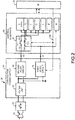
- Fig. 2 is a block diagram illustrating the structure of the power supply unit 20 and the structure of the control substrate 30 for controlling the supply of a supply voltage to each unit. Further, for the sake of convenience of description, the units in the control substrate 30 are represented by signs A-G.
- the unit A is the CPU 101
- the unit B is the monitoring unit 111 in the CPU 101.
- the unit C is the FAX unit 15
- the unit D is the drive section 141 of the control unit 14.
- the unit E is the scanner unit 12
- the unit F is the printer unit 13.
- the unit G is the mechanical system for conveying a sheet.
- the image forming apparatus 10 may comprise other units the detailed structure of which is not described herein.
- a main power switch 22 As shown in Fig. 2 , in the power supply unit 20, a main power switch 22, a low-voltage power supply 23 and an AC power supply 21 are connected in series . The voltage of the AC power supply 21 is supplied to the low-voltage power supply 23 by switching on the main power switch 22.
- the low-voltage power supply 23 comprises a filter unit 24, a first AC/DC circuit 25 and a second AC/DC circuit 26.
- the filter unit 24 removes unneeded noises.
- the first AC/DC circuit 25 and the second AC/DC circuit 26 convert an alternating voltage into a direct voltage.
- a direct voltage V1 is obtained from the first AC/DC circuit 25 and supplied to a first input terminal IN1 of the control substrate 30 as a first output voltage V1.
- a direct voltage V2 is obtained from the second AC/DC circuit 26 and supplied to a second input terminal IN2 of the control substrate 30 as a second output voltage V2.
- the first input terminal IN1 is connected with a first switch 311 of a switching circuit 31. Further, the second input terminal IN2 is connected with a second switch 312 of the switching circuit 31.
- the first input terminal IN1 and the second input terminal IN2 are selectively connected with a first output terminal P1 and a second output terminal P2 by switching on/off the first switch 311 and the second switch 312. Consequentially, the output voltage V1 and the output voltage V2 are selectively supplied to the output terminal P1 and the output terminal P2.
- the output terminal P1 of the switching circuit 31 is connected with the units A-F.
- the output terminal P2 is connected with the units B and D. That is, in the normal mode, the switch 311 of the switching circuit 31 is 'ON' so that the output voltage V1 from the first AC/DC circuit 25 is supplied to the units A-F via the switch 311. Further, the output voltage V1 is only supplied to the mechanical system G when the first AC/DC circuit 25 acts.
- the switch 312 of the switching circuit 31 is 'ON' so that the output voltage V2 from the second AC/DC circuit 26 is supplied to the units B and D via the switch 312.
- control panel 14 As a UI functioning under the control of the CPU 101, the control panel 14 generates a control signal 140 in response to an operation of the user or the action of a timer.
- the control signal 140 is supplied to the first AC/DC circuit 25 and the switching unit 31.
- the control signal 140 becomes a trigger for the transfer from the normal mode to the sleep mode and the transfer from the sleep mode to the normal mode.
- the first AC/DC circuit 25 acts, the switch 311 is switched on, and the switch 312 is switched off.
- the second AC/DC circuit 26 acts, the switch 312 is switched on, and the switch 311 is switched off.
- the switching circuit 31 may be a mechanical switch such as a relay or an electronic switch such as a semiconductor element.
- the output voltage V1 from the first AC/DC circuit 25 is supplied to the mechanical system G and the units A-F comprising a system and the image forming unit via the switching circuit 31, and in the sleep mode, the output voltage V2 from the second AC/DC circuit 26 is only supplied to the units B and D related to the control on the sleep mode via the switching circuit 31.
- the second AC/DC circuit 26 special for the units B and D related to the control on the sleep mode is characterized in specialization of the loads of the units B and D.
- the AC/DC circuit 26 is designed to be a high-efficiency AC/DC circuit having the maximum power-supply efficiency, matching with the units B and D serving as loads.
- the AC/DC circuit supplies power for the loads (A-F) in the normal mode. Further, in the sleep mode, the power of the loads (B, D) is obtained by a power transformer. Thus, in the sleep mode, the AC/DC circuit works to supply power for the loads B and D. However, the performance of the AC/DC circuit requires the AC/DC circuit to be capable of supplying power for the loads (units A-F) in the normal mode.
- the power-supply efficiency characteristic of the AC/DC circuit shows that the power-supply efficiency of the AC/DC circuit is likely to drop when the power consumption of the load is reduced.
- the power-supply efficiency is described below with reference to Fig. 3 .
- Fig. 3 is a diagram illustrating the characteristic of the power-supply efficiency of a low-voltage power supply.
- the horizontal axis represents the load of a secondary side
- the vertical axis represents power-supply efficiency (0-80%).
- the power-supply efficiency of the low-voltage power supply is reduced by the amount indicated by the arrow Y1, compared with that of the low-voltage power supply in the normal mode.
- the second AC/DC circuit 26 is designed to have the maximum power-supply efficiency matching with the units the load change of which is small. Thus, the power-supply efficiency in the sleep mode is improved.
- the output voltage V2 is output to the monitoring unit 111 of the CPU 101 and the drive section 141 of the control panel 14.
- the load of the monitoring unit 111 or the drive section 141 is reduced and slightly changed.
- the second AC/DC circuit 26 is designed to have the maximum power-supply efficiency matching with the loads in the sleep mode.
- the switching circuit 31 may also be arranged at the side of the low-voltage power supply 23.
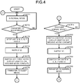
- Fig. 4 is a flowchart illustrating a mode control method according to an embodiment.
- Fig. 4 shows an example of the supply of the power from the power supply unit 20 under the control of the CPU 101.
- the CPU 101 causes the image forming apparatus 10 to act in the normal mode. At this time, the output voltage V1 from the first AC/DC circuit 25 is supplied to the loads (units A-G).
- the CPU 101 determines whether or not to transfer to the sleep mode. For example, the CPU 101 tries to transfer to the sleep mode if no operation is carried out within a preset period of time after an operation is carried out on the control panel 14.
- the CPU 101 stops the units A, C, E, F and G in Act 3 (OFF) .
- the CPU 101 supplies the output voltage V2 to loads (units B and D) to control the switching circuit 31 and carries out a switching to connect the switch 312 with the second output terminal P2.
- the switch 311 carries out a switching to disconnect the first input terminal IN1 from the first output terminal P1.
- the CPU 101 switches off the first AC/DC circuit 25 and switches on the second AC/DC circuit 26.
- the CPU 101 switches to the sleep mode in which the output voltage V2 is supplied from the second AC/DC circuit 26 to the units B and D via the switch 312 so that the units B and D act in the sleep mode.
- the monitoring unit 111 of the CPU 101 is in an action state. Even in the sleep mode, the condition of the access from the network 300 and the reception of a FAX by the FAX unit 15 are monitored by the monitoring unit 111.
- the CPU 101 determines whether or not to recover to the normal mode. For example, if the control panel 14 is operated in the sleep mode, then the normal mode is recovered according to the operation of the user. Further, the normal mode is recovered when the image forming apparatus is accessed from an external PC via the network 300.
- the CPU 101 switches on the first AC/DC circuit 25 in Act 12.
- the CPU 101 also switches off the second AC/DC circuit 26.
- the switching circuit 31 is controlled to connect the switch 311 with the first output terminal P1 and supply the output voltage V1 to loads (units A-F and G) .
- the switch 312 is switched to disconnect the second input terminal IN2 from the second output terminal P2.
- Act 14 the CPU 101 switches on the units A, C, E, F and G.
- Act 15 the image forming apparatus 10 recovers to the normal mode. After the Act 15, the flow returns to Act 1 to repeat the subsequent actions.
- the high efficiency of the low-voltage power supply 23 in the sleep mode can be sought to reduce power consumption.
- Fig. 5 is a block diagram illustrating the structures of the power supply unit 20 and the control substrate 30 of an electronic device (image forming apparatus) involved in the second embodiment.
- a plurality of AC/DC circuits are configured which act in the sleep mode.
- the low-voltage power supply 23 comprises a first AC/DC circuit 25, a second AC/DC circuit 26 and a third AC/DC circuit 27.
- the output voltage V1 is obtained from the first AC/DC circuit 25, and the output voltage V2 is obtained from the second AC/DC circuit 26.
- An output voltage V3 is obtained from the third AC/DC circuit 27.
- the switching circuit 31 further comprises a third input terminal IN3 and a third output terminal P3.
- the second input terminal IN2 and the third input terminal IN3 are connected with the second switch 312 and the third switch 313 which are linked with each other.
- the output voltage V2 and the output voltage V3 can be selectively supplied to the second output terminal P2 and the third output terminal P3 by switching on or off the second and the third switch 312 and 313. Further, as shown in Fig. 2 , the first switch 311 switches the state of the connection of the first input terminal IN1 with the output terminal P1.
- the output terminal P1 of the switching circuit 31 is connected with the units A-F.
- the output terminal P2 is connected with the units B and D, and the output terminal P3 is connected with the unit C. That is, in the normal mode, the switch 311 of the switching circuit 31 is 'ON' so that the output voltage V1 from the first AC/DC circuit 25 is supplied to the units A-F via the switch 311. Further, the output voltage V1 is only supplied to the mechanical system G when the first AC/DC circuit 25 acts.
- the switches 312 and 313 of the switching circuit 31 are 'ON' so that the output voltage V2 from the second AC/DC circuit 26 is supplied to the units B and D via the switch 312. Moreover, the output voltage V3 from the third AC/DC circuit 27 is supplied to the unit C via the switch 313.
- the control panel 14 As a UI functioning under the control of the CPU 101, the control panel 14 generates a control signal 140 in response to an operation of the user or the action of a timer.
- the control signal 140 is supplied to the switching unit 31.
- the control signal 140 in the normal mode, the first AC/DC circuit 25 acts, the switch 311 is 'ON', and the switches 312 and 313 are 'OFF'.
- the control signal 140 in the sleep mode, the second and the third AC/DC circuit 26 and 27 act, the switches 312 and 313 are 'ON', and the switch 311 is 'OFF'.
- the output voltage V2 from the second AC/DC circuit 26 is supplied to the units B and D via the switch 312, and the output voltage V3 from the third AC/DC circuit 27 is supplied to the unit C via the switch 313.
- the second AC/DC circuit 26 for the units B and D related to the control on the sleep mode can be characterized in specialization of the loads of the units B and D.
- the third AC/DC circuit 27 for the unit C related to the control on the sleep mode can be characterized in specialization of the loads of the unit C.
- the units B, D and C are designed as high-efficiency AC/DC circuits 26 and 27 having the maximum power-supply efficiency matching with the loads.
- the high efficiency of the low-voltage power supply in the sleep mode can be sought to reduce power consumption.
- a third AC/DC circuit 27 is arranged for the unit C.
- the unit C may also be activated by the AC/DC circuit 25 like the other units A, E and F and switched off in the sleep mode.
- a special second AC/DC circuit 26 may be arranged for the unit B, and a special third AC/DC circuit 27 may be arranged for the unit D.
- the present invention may have various applications, but not limited to the foregoing embodiments.
- the foregoing power supply unit 20 or control substrate 30 may be applied to other electronic devices which function in a normal mode and a sleep mode.
- the units B and D act in the sleep mode, however, other units may also act in the sleep mode. That is, the units acting in the sleep mode are determined matching with the actual circuits of an electronic device, and AC/DC circuits are arranged matching with the units.
Landscapes
- Physics & Mathematics (AREA)
- General Physics & Mathematics (AREA)
- Engineering & Computer Science (AREA)
- Microelectronics & Electronic Packaging (AREA)
- Control Or Security For Electrophotography (AREA)
- Accessory Devices And Overall Control Thereof (AREA)
Claims (10)
- Elektronische Vorrichtung (10) für ein Bilderzeugungsgerät, wobei die elektronische Vorrichtung in der Lage ist, in einem Gemeinsame-Aktion-Modus bzw. Gleichtaktaktionsmodus und einem Energiesparmodus zu arbeiten, umfassend:eine Mehrzahl von Einheiten, die konfiguriert sind, in dem Gleichtaktaktionsmodus (A, B, C, D, E, F) zu arbeiten;eine erste AC/DC-Schaltung (25), die konfiguriert ist, eine erste Gleichspannung (V1) der Mehrzahl von Einheiten (A, B, C, D, E, F) zuzuführen;eine zweite AC/DC-Schaltung (26), die konfiguriert ist, eine zweite Gleichspannung (V2) einer bestimmten (B, D) der Einheiten zuzuführen, die in dem Energiesparmodus arbeitet;eine Umschaltschaltung (31), die konfiguriert ist, ein Umschalten durchzuführen, so dass die erste Gleichspannung der Mehrzahl von Einheiten in dem Gleichtaktaktionsmodus zugeführt wird und die zweite Gleichspannung einer bestimmten Einheit in dem Energiesparmodus zugeführt wird;ein mechanisches System (G) zum Befördern eines Blatts, das konfiguriert ist, unabhängig von der Umschaltschaltung (31) die erste Gleichspannung (V1) aufzunehmen, immer wenn die erste AC/DC-Schaltung (25) arbeitet, undeine Steuer- bzw. Regeleinheit (101), die konfiguriert ist, zwischen dem Gleichtaktaktionsmodus und dem Energiesparmodus zu unterscheiden und den Schaltkreis zu steuern bzw. zu regeln,wobei das mechanische System (G) konfiguriert ist, die erste Gleichspannung (V1) aufzunehmen, immer wenn die erste AC/DC-Schaltung (25) die erste Gleichspannung liefert.
- Elektronische Vorrichtung nach Anspruch 1, wobei die zweite AC/DC-Schaltung so ausgebildet ist, dass die maximale Leistungsversorgungseffizienz mit der Last der spezifischen Einheit übereinstimmt.
- Elektronische Vorrichtung nach Anspruch 1 oder 2, wobei, wenn die Anzahl der spezifischen Einheiten, die in dem Energiesparmodus arbeiten, mehr als zwei beträgt, eine Mehrzahl zweiter AC/DC-Schaltungen separat entsprechend den spezifischen Einheiten angeordnet ist.
- Bilderzeugungsgerät, umfassend:ein vom Benutzer bedienbares Bedienfeld;eine elektronische Vorrichtung nach Anspruch 1, wobei die Mehrzahl von Einheiten, die konfiguriert sind, in dem Gleichtaktaktionsmodus zu arbeiten, eine Bilderzeugungseinheit zum Erzeugen eines Bildes auf einem Blatt enthält.
- Bilderzeugungsgerät nach Anspruch 4, wobei die zweite AC/DC-Schaltung so ausgebildet ist, dass die maximale Leistungsversorgungseffizienz mit der Last der spezifischen Einheit übereinstimmt.
- Bilderzeugungsgerät nach Anspruch 4 oder 5, wobei, wenn die Anzahl der spezifischen Einheiten, die in dem Energiesparmodus arbeiten, mehr als zwei beträgt, eine Mehrzahl zweiter AC/DC-Schaltungen separat entsprechend den spezifischen Einheiten angeordnet ist.
- Bilderzeugungsgerät nach einem der Ansprüche 4 bis 6, wobei die Steuer- bzw. Regeleinheit konfiguriert ist, eine Steuerung bzw. Regelung auszuführen, um den Gleichtaktaktionsmodus aus dem Energiesparmodus ansprechend auf die Bedienung auf dem Bedienfeld wiederherzustellen.
- Bilderzeugungsgerät nach einem der Ansprüche 4 bis 7, wobei die spezifischen Einheiten Teil einer CPU sind, welche die Steuer- bzw. Regeleinheit und eine Antriebseinheit zum Steuern bzw. Regeln der Aktionen des Bedienfelds bildet.
- Leistungsversorgungssteuer- bzw. -regelverfahren für eine elektronische Vorrichtung (10) für ein Bilderzeugungsgerät, wobei die elektronische Vorrichtung in der Lage ist, in einem Gemeinsame-Aktion-Modus bzw. Gleichtaktaktionsmodus und einem Energiesparmodus zu arbeiten, umfassend:Erzeugen, durch eine erste AC/DC-Schaltung (25), einer ersten Gleichspannung (V1) für eine Mehrzahl von Einheiten (A, B, C, D, E, F), die in dem Gleichtaktaktionsmodus arbeiten;Erzeugen, durch eine zweite AC/DC-Schaltung (26), einer zweiten Gleichspannung (V2) für die bestimmte (B, D) der Mehrzahl von Einheiten, die in dem Energiesparmodus arbeitet;Unterscheiden, durch eine Steuer- bzw. Regeleinheit (101), zwischen dem Gleichtaktaktionsmodus und dem Energiesparmodus; undSchalten, durch die Steuer- bzw. Regeleinheit (101), eines Schaltkreises, so dass die erste Gleichspannung (V1) der Mehrzahl von Einheiten in dem Gleichtaktmodus zugeführt wird und die zweite Gleichspannung (V2) der spezifischen Einheit in dem Energiesparmodus zugeführt wird,wobei ein mechanisches System (G) zum Befördern eines Blatts, das zu der elektronischen Vorrichtung gehört, konfiguriert ist, unabhängig von der Umschaltschaltung (31) die erste Gleichspannung (V1) aufzunehmen, immer wenn die erste AC/DC-Schaltung (25) die erste Gleichspannung liefert.
- Leistungsversorgungssteuer- bzw. -regelverfahren nach Anspruch 9, wobei die zweite AC/DC-Schaltung so ausgebildet ist, dass die maximale Leistungsversorgungseffizienz mit der Last der spezifischen Einheit übereinstimmt.
Priority Applications (1)
| Application Number | Priority Date | Filing Date | Title |
|---|---|---|---|
| EP15179994.7A EP3128371B1 (de) | 2015-08-06 | 2015-08-06 | Elektronische vorrichtung, bilderzeugungsvorrichtung und stromversorgungssteuerungsverfahren für elektronische vorrichtung |
Applications Claiming Priority (1)
| Application Number | Priority Date | Filing Date | Title |
|---|---|---|---|
| EP15179994.7A EP3128371B1 (de) | 2015-08-06 | 2015-08-06 | Elektronische vorrichtung, bilderzeugungsvorrichtung und stromversorgungssteuerungsverfahren für elektronische vorrichtung |
Publications (2)
| Publication Number | Publication Date |
|---|---|
| EP3128371A1 EP3128371A1 (de) | 2017-02-08 |
| EP3128371B1 true EP3128371B1 (de) | 2019-09-25 |
Family
ID=53835303
Family Applications (1)
| Application Number | Title | Priority Date | Filing Date |
|---|---|---|---|
| EP15179994.7A Active EP3128371B1 (de) | 2015-08-06 | 2015-08-06 | Elektronische vorrichtung, bilderzeugungsvorrichtung und stromversorgungssteuerungsverfahren für elektronische vorrichtung |
Country Status (1)
| Country | Link |
|---|---|
| EP (1) | EP3128371B1 (de) |
Family Cites Families (4)
| Publication number | Priority date | Publication date | Assignee | Title |
|---|---|---|---|---|
| JP2006184329A (ja) * | 2004-12-24 | 2006-07-13 | Ricoh Co Ltd | 画像形成装置 |
| JP5531005B2 (ja) * | 2011-12-26 | 2014-06-25 | 株式会社沖データ | 電子機器 |
| JP5899959B2 (ja) * | 2012-01-23 | 2016-04-06 | 株式会社リコー | 電源装置、電子機器及び画像形成装置 |
| JP5984514B2 (ja) * | 2012-05-31 | 2016-09-06 | キヤノン株式会社 | 電源装置およびそれを備えた画像形成装置 |
-
2015
- 2015-08-06 EP EP15179994.7A patent/EP3128371B1/de active Active
Non-Patent Citations (1)
| Title |
|---|
| None * |
Also Published As
| Publication number | Publication date |
|---|---|
| EP3128371A1 (de) | 2017-02-08 |
Similar Documents
| Publication | Publication Date | Title |
|---|---|---|
| US8170437B2 (en) | Operation display device and image forming apparatus equipped therewith | |
| EP2509030B1 (de) | Bilderzeugungsvorrichtung und Steuerverfahren dafür | |
| US7539886B2 (en) | Image processing apparatus, power saving control method, and program and storage medium thereof | |
| CN104113651B (zh) | 处理控制设备、图像处理设备和处理控制方法 | |
| CN103765344B (zh) | 具备多个显示装置的系统和图像处理装置 | |
| EP2395642B1 (de) | Schaltstromversorgung und Schaltstromversorgungsverfahren damit | |
| CN103248776B (zh) | 复印系统 | |
| EP3128371B1 (de) | Elektronische vorrichtung, bilderzeugungsvorrichtung und stromversorgungssteuerungsverfahren für elektronische vorrichtung | |
| US8564801B2 (en) | Network system, electronic device, and method for controlling electronic device in network system | |
| JP4333717B2 (ja) | 画像形成装置 | |
| US20210026287A1 (en) | Power supply apparatus and image forming apparatus | |
| US9247091B2 (en) | Image forming apparatus, control method for image forming apparatus, and program that stop supply of power to a printer unit and supply of power to a scanner unit based on elapsed times | |
| EP3128372B1 (de) | Elektronische vorrichtung, bilderzeugungsvorrichtung und stromversorgungssteuerungsverfahren für elektronische vorrichtung | |
| JP2008268326A (ja) | 画像形成装置および電源制御方法 | |
| JP2007116457A (ja) | 画像形成装置 | |
| US9031445B2 (en) | Power saving modes in an image forming apparatus | |
| JP5821406B2 (ja) | 画像処理装置、省電力制御方法及び省電力制御プログラム | |
| JP6171550B2 (ja) | 電源制御装置及び画像処理装置 | |
| JP6477757B2 (ja) | 画像形成システム | |
| JP7218562B2 (ja) | 電子機器、電源制御システム、電源制御方法およびプログラム | |
| JP5808136B2 (ja) | 画像形成装置、その制御方法、及びプログラム | |
| JP5831071B2 (ja) | 画像形成装置及び印刷システム並びに起動制御方法並びにプログラム | |
| US9065956B2 (en) | Information processing apparatus and control method for information processing apparatus | |
| JP2017124558A (ja) | 画像形成装置 |
Legal Events
| Date | Code | Title | Description |
|---|---|---|---|
| PUAI | Public reference made under article 153(3) epc to a published international application that has entered the european phase |
Free format text: ORIGINAL CODE: 0009012 |
|
| STAA | Information on the status of an ep patent application or granted ep patent |
Free format text: STATUS: THE APPLICATION HAS BEEN PUBLISHED |
|
| AK | Designated contracting states |
Kind code of ref document: A1 Designated state(s): AL AT BE BG CH CY CZ DE DK EE ES FI FR GB GR HR HU IE IS IT LI LT LU LV MC MK MT NL NO PL PT RO RS SE SI SK SM TR |
|
| AX | Request for extension of the european patent |
Extension state: BA ME |
|
| STAA | Information on the status of an ep patent application or granted ep patent |
Free format text: STATUS: REQUEST FOR EXAMINATION WAS MADE |
|
| 17P | Request for examination filed |
Effective date: 20170808 |
|
| RBV | Designated contracting states (corrected) |
Designated state(s): AL AT BE BG CH CY CZ DE DK EE ES FI FR GB GR HR HU IE IS IT LI LT LU LV MC MK MT NL NO PL PT RO RS SE SI SK SM TR |
|
| STAA | Information on the status of an ep patent application or granted ep patent |
Free format text: STATUS: EXAMINATION IS IN PROGRESS |
|
| 17Q | First examination report despatched |
Effective date: 20180329 |
|
| GRAP | Despatch of communication of intention to grant a patent |
Free format text: ORIGINAL CODE: EPIDOSNIGR1 |
|
| STAA | Information on the status of an ep patent application or granted ep patent |
Free format text: STATUS: GRANT OF PATENT IS INTENDED |
|
| INTG | Intention to grant announced |
Effective date: 20190318 |
|
| RIN1 | Information on inventor provided before grant (corrected) |
Inventor name: OTAKI, MITSUHIKO |
|
| GRAS | Grant fee paid |
Free format text: ORIGINAL CODE: EPIDOSNIGR3 |
|
| RAP1 | Party data changed (applicant data changed or rights of an application transferred) |
Owner name: KABUSHIKI KAISHA TOSHIBA Owner name: TOSHIBA TEC KABUSHIKI KAISHA |
|
| GRAA | (expected) grant |
Free format text: ORIGINAL CODE: 0009210 |
|
| STAA | Information on the status of an ep patent application or granted ep patent |
Free format text: STATUS: THE PATENT HAS BEEN GRANTED |
|
| AK | Designated contracting states |
Kind code of ref document: B1 Designated state(s): AL AT BE BG CH CY CZ DE DK EE ES FI FR GB GR HR HU IE IS IT LI LT LU LV MC MK MT NL NO PL PT RO RS SE SI SK SM TR |
|
| REG | Reference to a national code |
Ref country code: GB Ref legal event code: FG4D |
|
| REG | Reference to a national code |
Ref country code: CH Ref legal event code: EP |
|
| REG | Reference to a national code |
Ref country code: DE Ref legal event code: R096 Ref document number: 602015038561 Country of ref document: DE |
|
| REG | Reference to a national code |
Ref country code: AT Ref legal event code: REF Ref document number: 1184392 Country of ref document: AT Kind code of ref document: T Effective date: 20191015 |
|
| REG | Reference to a national code |
Ref country code: IE Ref legal event code: FG4D |
|
| REG | Reference to a national code |
Ref country code: NL Ref legal event code: MP Effective date: 20190925 |
|
| PG25 | Lapsed in a contracting state [announced via postgrant information from national office to epo] |
Ref country code: BG Free format text: LAPSE BECAUSE OF FAILURE TO SUBMIT A TRANSLATION OF THE DESCRIPTION OR TO PAY THE FEE WITHIN THE PRESCRIBED TIME-LIMIT Effective date: 20191225 Ref country code: SE Free format text: LAPSE BECAUSE OF FAILURE TO SUBMIT A TRANSLATION OF THE DESCRIPTION OR TO PAY THE FEE WITHIN THE PRESCRIBED TIME-LIMIT Effective date: 20190925 Ref country code: NO Free format text: LAPSE BECAUSE OF FAILURE TO SUBMIT A TRANSLATION OF THE DESCRIPTION OR TO PAY THE FEE WITHIN THE PRESCRIBED TIME-LIMIT Effective date: 20191225 Ref country code: FI Free format text: LAPSE BECAUSE OF FAILURE TO SUBMIT A TRANSLATION OF THE DESCRIPTION OR TO PAY THE FEE WITHIN THE PRESCRIBED TIME-LIMIT Effective date: 20190925 Ref country code: LT Free format text: LAPSE BECAUSE OF FAILURE TO SUBMIT A TRANSLATION OF THE DESCRIPTION OR TO PAY THE FEE WITHIN THE PRESCRIBED TIME-LIMIT Effective date: 20190925 Ref country code: HR Free format text: LAPSE BECAUSE OF FAILURE TO SUBMIT A TRANSLATION OF THE DESCRIPTION OR TO PAY THE FEE WITHIN THE PRESCRIBED TIME-LIMIT Effective date: 20190925 |
|
| REG | Reference to a national code |
Ref country code: LT Ref legal event code: MG4D |
|
| PG25 | Lapsed in a contracting state [announced via postgrant information from national office to epo] |
Ref country code: LV Free format text: LAPSE BECAUSE OF FAILURE TO SUBMIT A TRANSLATION OF THE DESCRIPTION OR TO PAY THE FEE WITHIN THE PRESCRIBED TIME-LIMIT Effective date: 20190925 Ref country code: GR Free format text: LAPSE BECAUSE OF FAILURE TO SUBMIT A TRANSLATION OF THE DESCRIPTION OR TO PAY THE FEE WITHIN THE PRESCRIBED TIME-LIMIT Effective date: 20191226 Ref country code: RS Free format text: LAPSE BECAUSE OF FAILURE TO SUBMIT A TRANSLATION OF THE DESCRIPTION OR TO PAY THE FEE WITHIN THE PRESCRIBED TIME-LIMIT Effective date: 20190925 |
|
| REG | Reference to a national code |
Ref country code: AT Ref legal event code: MK05 Ref document number: 1184392 Country of ref document: AT Kind code of ref document: T Effective date: 20190925 |
|
| PG25 | Lapsed in a contracting state [announced via postgrant information from national office to epo] |
Ref country code: ES Free format text: LAPSE BECAUSE OF FAILURE TO SUBMIT A TRANSLATION OF THE DESCRIPTION OR TO PAY THE FEE WITHIN THE PRESCRIBED TIME-LIMIT Effective date: 20190925 Ref country code: PT Free format text: LAPSE BECAUSE OF FAILURE TO SUBMIT A TRANSLATION OF THE DESCRIPTION OR TO PAY THE FEE WITHIN THE PRESCRIBED TIME-LIMIT Effective date: 20200127 Ref country code: AL Free format text: LAPSE BECAUSE OF FAILURE TO SUBMIT A TRANSLATION OF THE DESCRIPTION OR TO PAY THE FEE WITHIN THE PRESCRIBED TIME-LIMIT Effective date: 20190925 Ref country code: EE Free format text: LAPSE BECAUSE OF FAILURE TO SUBMIT A TRANSLATION OF THE DESCRIPTION OR TO PAY THE FEE WITHIN THE PRESCRIBED TIME-LIMIT Effective date: 20190925 Ref country code: IT Free format text: LAPSE BECAUSE OF FAILURE TO SUBMIT A TRANSLATION OF THE DESCRIPTION OR TO PAY THE FEE WITHIN THE PRESCRIBED TIME-LIMIT Effective date: 20190925 Ref country code: PL Free format text: LAPSE BECAUSE OF FAILURE TO SUBMIT A TRANSLATION OF THE DESCRIPTION OR TO PAY THE FEE WITHIN THE PRESCRIBED TIME-LIMIT Effective date: 20190925 Ref country code: NL Free format text: LAPSE BECAUSE OF FAILURE TO SUBMIT A TRANSLATION OF THE DESCRIPTION OR TO PAY THE FEE WITHIN THE PRESCRIBED TIME-LIMIT Effective date: 20190925 Ref country code: AT Free format text: LAPSE BECAUSE OF FAILURE TO SUBMIT A TRANSLATION OF THE DESCRIPTION OR TO PAY THE FEE WITHIN THE PRESCRIBED TIME-LIMIT Effective date: 20190925 Ref country code: RO Free format text: LAPSE BECAUSE OF FAILURE TO SUBMIT A TRANSLATION OF THE DESCRIPTION OR TO PAY THE FEE WITHIN THE PRESCRIBED TIME-LIMIT Effective date: 20190925 |
|
| PG25 | Lapsed in a contracting state [announced via postgrant information from national office to epo] |
Ref country code: CZ Free format text: LAPSE BECAUSE OF FAILURE TO SUBMIT A TRANSLATION OF THE DESCRIPTION OR TO PAY THE FEE WITHIN THE PRESCRIBED TIME-LIMIT Effective date: 20190925 Ref country code: SK Free format text: LAPSE BECAUSE OF FAILURE TO SUBMIT A TRANSLATION OF THE DESCRIPTION OR TO PAY THE FEE WITHIN THE PRESCRIBED TIME-LIMIT Effective date: 20190925 Ref country code: IS Free format text: LAPSE BECAUSE OF FAILURE TO SUBMIT A TRANSLATION OF THE DESCRIPTION OR TO PAY THE FEE WITHIN THE PRESCRIBED TIME-LIMIT Effective date: 20200224 Ref country code: SM Free format text: LAPSE BECAUSE OF FAILURE TO SUBMIT A TRANSLATION OF THE DESCRIPTION OR TO PAY THE FEE WITHIN THE PRESCRIBED TIME-LIMIT Effective date: 20190925 |
|
| REG | Reference to a national code |
Ref country code: DE Ref legal event code: R097 Ref document number: 602015038561 Country of ref document: DE |
|
| PG2D | Information on lapse in contracting state deleted |
Ref country code: IS |
|
| PG25 | Lapsed in a contracting state [announced via postgrant information from national office to epo] |
Ref country code: DK Free format text: LAPSE BECAUSE OF FAILURE TO SUBMIT A TRANSLATION OF THE DESCRIPTION OR TO PAY THE FEE WITHIN THE PRESCRIBED TIME-LIMIT Effective date: 20190925 Ref country code: IS Free format text: LAPSE BECAUSE OF FAILURE TO SUBMIT A TRANSLATION OF THE DESCRIPTION OR TO PAY THE FEE WITHIN THE PRESCRIBED TIME-LIMIT Effective date: 20200126 |
|
| PLBE | No opposition filed within time limit |
Free format text: ORIGINAL CODE: 0009261 |
|
| STAA | Information on the status of an ep patent application or granted ep patent |
Free format text: STATUS: NO OPPOSITION FILED WITHIN TIME LIMIT |
|
| 26N | No opposition filed |
Effective date: 20200626 |
|
| PGFP | Annual fee paid to national office [announced via postgrant information from national office to epo] |
Ref country code: FR Payment date: 20200715 Year of fee payment: 6 Ref country code: DE Payment date: 20200722 Year of fee payment: 6 Ref country code: GB Payment date: 20200729 Year of fee payment: 6 |
|
| PG25 | Lapsed in a contracting state [announced via postgrant information from national office to epo] |
Ref country code: SI Free format text: LAPSE BECAUSE OF FAILURE TO SUBMIT A TRANSLATION OF THE DESCRIPTION OR TO PAY THE FEE WITHIN THE PRESCRIBED TIME-LIMIT Effective date: 20190925 |
|
| PG25 | Lapsed in a contracting state [announced via postgrant information from national office to epo] |
Ref country code: MC Free format text: LAPSE BECAUSE OF FAILURE TO SUBMIT A TRANSLATION OF THE DESCRIPTION OR TO PAY THE FEE WITHIN THE PRESCRIBED TIME-LIMIT Effective date: 20190925 |
|
| REG | Reference to a national code |
Ref country code: CH Ref legal event code: PL |
|
| PG25 | Lapsed in a contracting state [announced via postgrant information from national office to epo] |
Ref country code: CH Free format text: LAPSE BECAUSE OF NON-PAYMENT OF DUE FEES Effective date: 20200831 Ref country code: LU Free format text: LAPSE BECAUSE OF NON-PAYMENT OF DUE FEES Effective date: 20200806 Ref country code: LI Free format text: LAPSE BECAUSE OF NON-PAYMENT OF DUE FEES Effective date: 20200831 |
|
| REG | Reference to a national code |
Ref country code: BE Ref legal event code: MM Effective date: 20200831 |
|
| PG25 | Lapsed in a contracting state [announced via postgrant information from national office to epo] |
Ref country code: IE Free format text: LAPSE BECAUSE OF NON-PAYMENT OF DUE FEES Effective date: 20200806 Ref country code: BE Free format text: LAPSE BECAUSE OF NON-PAYMENT OF DUE FEES Effective date: 20200831 |
|
| REG | Reference to a national code |
Ref country code: DE Ref legal event code: R119 Ref document number: 602015038561 Country of ref document: DE |
|
| GBPC | Gb: european patent ceased through non-payment of renewal fee |
Effective date: 20210806 |
|
| PG25 | Lapsed in a contracting state [announced via postgrant information from national office to epo] |
Ref country code: TR Free format text: LAPSE BECAUSE OF FAILURE TO SUBMIT A TRANSLATION OF THE DESCRIPTION OR TO PAY THE FEE WITHIN THE PRESCRIBED TIME-LIMIT Effective date: 20190925 Ref country code: MT Free format text: LAPSE BECAUSE OF FAILURE TO SUBMIT A TRANSLATION OF THE DESCRIPTION OR TO PAY THE FEE WITHIN THE PRESCRIBED TIME-LIMIT Effective date: 20190925 Ref country code: CY Free format text: LAPSE BECAUSE OF FAILURE TO SUBMIT A TRANSLATION OF THE DESCRIPTION OR TO PAY THE FEE WITHIN THE PRESCRIBED TIME-LIMIT Effective date: 20190925 |
|
| PG25 | Lapsed in a contracting state [announced via postgrant information from national office to epo] |
Ref country code: MK Free format text: LAPSE BECAUSE OF FAILURE TO SUBMIT A TRANSLATION OF THE DESCRIPTION OR TO PAY THE FEE WITHIN THE PRESCRIBED TIME-LIMIT Effective date: 20190925 |
|
| PG25 | Lapsed in a contracting state [announced via postgrant information from national office to epo] |
Ref country code: GB Free format text: LAPSE BECAUSE OF NON-PAYMENT OF DUE FEES Effective date: 20210806 Ref country code: FR Free format text: LAPSE BECAUSE OF NON-PAYMENT OF DUE FEES Effective date: 20210831 Ref country code: DE Free format text: LAPSE BECAUSE OF NON-PAYMENT OF DUE FEES Effective date: 20220301 |