EP3128372B1 - Elektronische vorrichtung, bilderzeugungsvorrichtung und stromversorgungssteuerungsverfahren für elektronische vorrichtung - Google Patents
Elektronische vorrichtung, bilderzeugungsvorrichtung und stromversorgungssteuerungsverfahren für elektronische vorrichtung Download PDFInfo
- Publication number
- EP3128372B1 EP3128372B1 EP15179996.2A EP15179996A EP3128372B1 EP 3128372 B1 EP3128372 B1 EP 3128372B1 EP 15179996 A EP15179996 A EP 15179996A EP 3128372 B1 EP3128372 B1 EP 3128372B1
- Authority
- EP
- European Patent Office
- Prior art keywords
- circuit
- power storage
- unit
- image forming
- storage device
- Prior art date
- Legal status (The legal status is an assumption and is not a legal conclusion. Google has not performed a legal analysis and makes no representation as to the accuracy of the status listed.)
- Not-in-force
Links
Images


Classifications
-
- G—PHYSICS
- G03—PHOTOGRAPHY; CINEMATOGRAPHY; ANALOGOUS TECHNIQUES USING WAVES OTHER THAN OPTICAL WAVES; ELECTROGRAPHY; HOLOGRAPHY
- G03G—ELECTROGRAPHY; ELECTROPHOTOGRAPHY; MAGNETOGRAPHY
- G03G15/00—Apparatus for electrographic processes using a charge pattern
- G03G15/50—Machine control of apparatus for electrographic processes using a charge pattern, e.g. regulating differents parts of the machine, multimode copiers, microprocessor control
- G03G15/5004—Power supply control, e.g. power-saving mode, automatic power turn-off
-
- G—PHYSICS
- G03—PHOTOGRAPHY; CINEMATOGRAPHY; ANALOGOUS TECHNIQUES USING WAVES OTHER THAN OPTICAL WAVES; ELECTROGRAPHY; HOLOGRAPHY
- G03G—ELECTROGRAPHY; ELECTROPHOTOGRAPHY; MAGNETOGRAPHY
- G03G15/00—Apparatus for electrographic processes using a charge pattern
- G03G15/80—Details relating to power supplies, circuits boards, electrical connections
Definitions
- Embodiments described herein relate to an electronic device such as an image forming apparatus and a power supply control method for reducing the power consumption of the electronic device acting in a power saving mode.
- a scanner unit and a printer unit are arranged in an electronic device such as an image forming apparatus, the scanner unit reads an original, the image data of the read original is processed by an image processing unit, and then the image data is printed by the printer unit.
- a digital multi-function peripheral is further provided with a public-line based FAX function in addition to a copy or scan function.
- the digital multi-function peripheral also has a plurality of functions, including a function of inputting print data from an external PC and printing and outputting the print data through the connection with a network and the cooperation with an external information processing apparatus (e.g. PC (Personal Computer)).
- PC Personal Computer
- an image forming apparatus which is enabled to act in a common action mode and a power saving mode acts in the power saving mode when not required to form an image.
- a first power circuit e.g. an AC/DC circuit
- the output terminal of the first power circuit is connected with an electrolytic capacitor so as to stabilize an output voltage.
- a second power circuit is arranged to supply power for a specific load. Moreover, the second power circuit supplies power when the common action mode is switched to the power saving mode.
- an electronic device is provided in accordance with appended claim 1.
- the power storage device is a device which is connected with the output terminal of the first AC/DC circuit and can be charged and discharged.
- the power storage device is an electrolytic capacitor for stabilizing the first direct voltage.
- the present invention relates to an image forming apparatus in accordance with appended claim 4.
- the power storage device is a device which is connected with the output terminal of the first AC/DC circuit and can be charged and discharged.
- the power storage device is an electrolytic capacitor for stabilizing the first direct voltage.
- control unit carries out a control to recover to the common action mode from the power saving mode in response to the operation on the control panel.
- the specific units are a part of a CPU constituting the control unit and a drive unit for controlling the actions of the control panel.
- the present invention further relates to a power supply control method in accordance with appended claim 9.
- the power storage device is a device which is connected with the output terminal of the first AC/DC circuit and can be charged and discharged with the first direct voltage.
- Fig. 1 is a block diagram illustrating an electronic device (image forming apparatus) involved in the first embodiment.
- an image forming apparatus is shown as an example of an electronic device.
- the image forming apparatus shown in Fig. 1 functions as, for example, a Multi-Function Peripheral (MFP).
- MFP Multi-Function Peripheral
- the MFP 10 comprises a control unit 11, a scanner unit 12, a printer unit 13, a control panel 14, a FAX unit 15 and a hard disk drive (HDD) serving as a memory unit.
- the MFP 10 further comprises a power supply unit 20 for supplying a supply voltage for each other unit of the MFP 10.
- the control unit 11 comprises a CPU 101, a ROM 102, a RAM 103 and a communication interface (I/F) 104 connected with a network 300.
- the CPU 101 controls the whole actions of the MFP 10.
- the control program of the CPU 101 is stored in the ROM 102.
- the RAM 103 provides a temporary work area for the CPU 101.
- a monitoring unit 111 which acts in the power saving mode is arranged in the CPU 101.
- the communication interface (I/F) 104 is connected with an external device such as a PC via the network 300 to receive the image data sent from the PC. Further, the control unit 11 is connected with the scanner unit 12, the printer unit 13, the control panel 14, the FAX unit 15 and the HDD 16.
- the control unit 11 compresses the image data read by the scanner unit 12 and stores the compressed image data in the HDD 16. Further, the image data received from the external device such as a PC is compressed and stored in the HDD 16. The control unit 11 reads the image data stored in the HDD 16, carries out an extension processing for the image data and then a specified image processing (e.g. gradation reproduction) and outputs the processed image data to the printer unit 13.
- the storage of image data in the HDD 16 and the reading of image data from the HDD 16 are both carried out under the control of the CPU 101.
- the control panel 14 comprises a drive section 141, various operation keys 142, a display 143 composed of liquid crystal and the like, a backlight 144 of liquid crystal and a touch panel 145 integrated with the display 143.
- the drive section 141 drives the display 143 to display various contents thereon. Further, the drive section 141 controls the backlight 144 to control the brightness of the display 143.
- the operation keys 142 input various instructions such as 'print copies'.
- the scanner unit 12 reads an original placed on an original table.
- the printer unit 13 including a photoconductive drum and a laser source scans and exposes the surface of the photoconductive drum with laser beams emitted from the laser source to generate an electrostatic latent image on the photoconductive drum.
- a charger, a developer and a transfer device are arranged around the photoconductive drum, and the electrostatic latent image on the photoconductive drum is developed by the developer to form a toner image on the photoconductive drum.
- the toner image is transferred onto a sheet by the transfer device.
- a fixer 17 is also arranged in the printer unit 13. A sheet transferred with a toner image is conveyed towards the fixer 17.
- the scanner unit 12 and the printer unit 13 which form an image on a sheet in response to an operation on the control panel 14 constitute an image forming unit. Further, the printer unit 13 may be of various other known structures, but not limited to the foregoing example.
- the FAX unit 15 which sends and receives data via a line 200 includes a FAX control unit 151 and a Network Control Unit (NCU) 152.
- NCU Network Control Unit
- the power supply unit 20 supplies various supply voltages for the other units in the MFP 10.
- the power supply unit 20 outputs a first output voltage V1 and a second output voltage V2 according to the common action mode and the power saving mode and supplies a supply voltage to a circuit in need of the supply voltage.
- the image forming apparatus 10 carries out a control to supply a supply voltage to each unit in the common action mode (hereinafter referred to as a normal mode) to cause each unit to act normally. Further, in the power saving mode (hereinafter referred to as a sleep mode), only the minimum required circuits are supplied with a supply voltage.
- a normal mode common action mode
- a sleep mode only the minimum required circuits are supplied with a supply voltage.
- the output voltage V1 from the power supply unit 20 is supplied to the control unit 11, the scanner unit 12, the printer unit 13, the control panel 14 and the FAX unit 15.
- the output voltage V1 is also supplied to a mechanical system for conveying a sheet.
- the CPU 101 of the control unit 11 is in a sleep state, only the monitoring unit 111 is in an action state. That is, as the access from the network 300 and the reception of a FAX by the FAX unit 15 are monitored even in the sleep mode, the monitoring unit 111 is active even in the sleep mode.
- the CPU 101 further comprises an internal timer. Moreover, the normal mode is switched to the sleep mode if no operation is carried out by the control panel 14 within a preset period of time in the normal mode.
- the sleep mode only the backlight 144 in the control panel 14 is 'OFF', the drive section 141 and the other units are in an action state. That is, if the user operates the control panel 14 in the sleep mode, then the normal mode can be recovered to according to the operation of the user.
- the control panel 14 functions as a User Interface (UI) .
- UI User Interface
- the control panel 14 informs, via the control unit 11, the power supply unit 20 of the transfer to the sleep mode or a trigger for the recovery of the normal mode from the sleep mode.
- the action mode of each of the CPU 101, the scanner unit 12, the printer unit 13, the control panel 14 and the FAX unit 15 can be optionally set by controlling the 'on/off' state of the unit.
- Fig. 2 is a block diagram illustrating the structure of the power supply unit 20 and the structure of the control substrate 30 for controlling the supply of the supply voltage to each unit. Further, for the sake of convenience of description, the units in the control substrate 30 are represented by signs A-G.
- the unit A is the CPU 101
- the unit B is the monitoring unit 111 in the CPU 101.
- the unit C is the FAX unit 15
- the unit D is the drive section 141 of the control unit 14.
- the unit E is the scanner unit 12
- the unit F is the printer unit 13.
- the unit G is the mechanical system for conveying a sheet.
- the image forming apparatus 10 may comprise other units the detailed structure of which is not described herein, but not limited to the units A-G.
- a main power switch 22 As shown in Fig. 2 , in the power supply unit 20, a main power switch 22, a low-voltage power supply 23 and an AC power supply 21 are connected in series. The voltage from the AC power supply 21 is supplied to the low-voltage power supply 23 by switching on the main power switch 22.
- the low-voltage power supply 23 comprises a filter unit 24, a first AC/DC circuit 25, a second AC/DC circuit 26 and a power switch 27.
- the filter unit 24 removes unneeded noises.
- the first AC/DC circuit 25 and the second AC/DC circuit 26 convert an alternating voltage into a direct voltage.
- the power switch 27 carries out an 'ON • OFF' control for the supply of an alternating voltage to the first AC/DC circuit 25.
- a direct voltage V1 is obtained from the first AC/DC circuit 25. Further, the output terminal of the first AC/DC circuit 25 is connected with an electrolytic capacitor 28 so as to stabilize the direct voltage V1.
- the electrolytic capacitor 28 constitutes a power storage device.
- the direct voltage V1 is supplied to a first input terminal IN1 of the control substrate 30 as a first output voltage V1.
- a direct voltage V2 is obtained from the second AC/DC circuit 26 and supplied to a second input terminal IN2 of the control substrate 30 as a second output voltage V2.
- the first input terminal IN1 is connected with a first switch 311 of a switching circuit 31. Further, the second input terminal IN2 is connected with a second switch 312 of the switching circuit 31.
- the first input terminal IN1 and the second input terminal IN2 are selectively connected with a first output terminal P1 and a second output terminal P2 by switching on/off the first switch 311 and the second switch 312. Consequentially, the output voltage V1 and the output voltage V2 are selectively supplied to the output terminal P1 and the output terminal P2.
- the switching circuit 31 may be a mechanical switch such as a relay or an electronic switch such as a semiconductor element.
- a voltage monitoring unit 32 is arranged on the control substrate 30 to monitor the power storage condition of the electrolytic capacitor 28.
- the voltage monitoring unit 32 consists of a comparator circuit 33 and a switch 34.
- a first input terminal of the comparator circuit 33 is supplied with the output voltage V1 which is the voltage between two terminals of the electrolytic capacitor 28.
- a reference voltage V0 is supplied to a second input terminal of the comparator circuit 33.
- the comparator circuit 33 generates an output signal when the output voltage V1 is below the reference voltage V0. That is, it is assumed that the reference voltage V0 is a threshold and the comparator circuit 33 generates an output signal when the output voltage V1 is below the threshold.
- the switching circuit 31 switches the state of a switch according to a control signal 140 (described later).
- the switch 34 is configured to control the supply of the control signal 140 to the switching circuit 31.
- the switch 34 which is an electronic switch serving as a semiconductor device is switched on according to an output signal of the comparator circuit 33.
- the output terminal P1 of the switching circuit 31 is connected with the units A-F.
- the output terminal P2 is connected with the units B and D. That is, in the normal mode, the control signal 140 is in a first state (e.g. at a zero level), and the switch 311 of the switching circuit 31 is 'ON' so that the output voltage V1 from the first AC/DC circuit 25 is supplied to the units A-F via the switch 311. Further, the output voltage V1 is only supplied to the mechanical system G when the first AC/DC circuit 25 acts.
- the control signal 140 is in a second state (e.g. at a high level), if the switch 34 is 'ON', then the switch 312 of the switching circuit 31 is 'ON' so that the output voltage V2 from the second AC/DC circuit 26 is supplied to the units B and D via the switch 312.
- control panel 14 As a UI functioning under the control of the CPU 101, the control panel 14 generates a control signal 140 in response to an operation of the user or the action of a timer.
- the control signal 140 is supplied to the power switch 27. Further, the control signal 140 is supplied to the switching unit 31 via the switch 34.
- the control signal 140 triggers the transfer from the normal mode to the sleep mode or the transfer from the sleep mode to the normal mode.
- the control signal 140 is at a zero level, the power switch 27 is 'ON', and the first AC/DC circuit 25 acts.
- the second AC/DC circuit 26 stops running.
- the first AC/DC circuit 25 acts to generate the output voltage V1, when the voltage V1 is above the reference voltage V0, no output signal is obtained from the comparator circuit 33, and the switch 34 is 'OFF'. In this case, the switch 311 of the switching circuit 31 is 'ON', and the switch 312 is 'OFF'.
- the first AC/DC circuit 25 stops acting and the second AC/DC circuit 26 acts.
- the output voltage V2 is supplied to the input terminal IN2, and the control signal 140 is at a high level.
- the voltage V1 at the first input terminal of the comparator circuit 33 is gradually reduced as the electrolytic capacitor 28 discharges.
- the comparator circuit 33 generates an output signal to switch on the switch 34 when the output voltage V1 is below the reference voltage V0.
- the high-level control signal 140 is supplied to the switching unit 31.
- the switch 312 is 'ON', and the switch 311 is 'OFF'.
- the output voltage V1 from the first AC/DC circuit 25 is supplied to the mechanical system G and the units A-F comprising a system and the image forming unit via the switching circuit 31 in the normal mode. Further, in the sleep mode, the switch 311 is 'ON' during the period in which the voltage between two terminals of the electrolytic capacitor 28 is higher than the threshold (reference voltage V0), thus, the voltage of the electrolytic capacitor 28 is supplied by the output terminal P1.
- the switch 311 of the switching circuit 31 is 'OFF', and the switch 312 is 'ON'. In this way, the output voltage V2 from the second AC/DC circuit 26 is only supplied to the units B and D related to a sleep mode control.
- the output voltage V1 which depends upon the electrolytic capacitor 28 is reduced as time elapses.
- the output voltage V1 is monitored by the voltage monitoring unit 32 so that the state of the switch 31 is switched when the output voltage V1 is below the threshold voltage V0.
- control substrate 30 at a secondary side is substantially in a load-free state during the period of the switching from the output voltage V1 of the first AC/DC circuit 25 to the output voltage V2 of the second AC/DC circuit 26. That is, the image forming apparatus acts by means of the voltage of the electrolytic capacitor 28 during this period, the power consumption of the first AC/DC circuit 25 and the second AC/DC circuit 26 are approximate to zero watt, thus reducing power consumption.
- the special second AC/DC circuit 26 related to a sleep mode control is characterized in having loads which are specialized as units B and D. In the sleep mode, the units B and D are unchanged or slightly changed in load. Thus, matching with the units B and D serving as loads, the AC/DC circuit 26 is designed as a high-efficiency AC/DC circuit having the maximum power efficiency.
- Fig. 3 is a diagram illustrating the actions of the voltage monitoring unit 32.
- the vertical axis represents the output voltage V1
- the horizontal axis represents time.
- the period from T0 to T1 represents a normal mode.
- the control signal 140 is changed from a low level to a high level, as shown in Fig. 3B .
- the switch 34 is switched off even if the control signal 140 is of high level, thus, the control signal 140 supplied to the switching circuit 31 is of zero level, and the switching circuit 31 keeps the current state rather than make a switching.
- the output voltage V1 is gradually reduced in the sleep mode. If the output voltage V1 turns to be below the threshold (reference voltage V0) at the timing T2, then the switch 34 is switched on according to an output signal from the comparator circuit 33. Thus, the high-level control signal 140 is supplied to the switching unit 31, as shown in Fig. 3C .
- the switching circuit 31 switches on the switch 312 and switches off the switch 311 according to the control signal 140. That is, the actions carried out based on the output voltage V1 are not switched to those carried out based on the output voltage V2 immediately even when the mode is switched to the sleep mode, but switched until the period in which the voltage of the electrolytic capacitor 28 is reduced to a given value.
- the loads act during the period (T1-T2) according to the voltage of the electrolytic capacitor 28, consequentially, the power consumption of the first AC/DC circuit 25 and the second AC/DC circuit 26 are approximate to zero watt.
- switching circuit 31 and the voltage monitoring unit 32 are arranged at the side of the control substrate 30 in the embodiment shown in Fig. 2 , the switching circuit 31 may also be arranged at the side of the low-voltage power supply 23.
- Fig. 4 is a flowchart illustrating a mode control method according to an embodiment.
- Fig. 4 shows an example of the power supply from the power supply unit 20 under the control of the CPU 101.
- the CPU 101 causes the image forming apparatus 10 to act in the normal mode. At this time, the output voltage V1 from the first AC/DC circuit 25 is supplied to loads (units A-G).
- the CPU 101 determines whether or not to transfer to the sleep mode. For example, the CPU 101 tries to transfer to the sleep mode if no operation is carried out within a preset period of time after an operation is carried out in the control panel 14.
- the CPU 101 stops (switches off) the units A, C, E, F and G in Act 3. In Act 4, the CPU 101 switches off the second AC/DC circuit 25. Further, in Act 5, the CPU 101 transfers to the sleep mode and switches on the second AC/DC circuit 26.
- the voltage monitoring unit 32 monitors the first output voltage V1.
- the voltage monitoring unit 32 determines whether or not the output voltage V1 is below the threshold (reference voltage V0) and switches on the switch 34 when the output voltage V1 is below the threshold so as to supply the control signal 140 to the switching circuit 31.
- the switching circuit 31 supplies the second output voltage V2 to loads (units B and D), thus, the switch 312 is switched to be connected with the second output terminal P2. At this time, the switch 311 is switched to disconnect the first input terminal IN1 from the first output terminal P1 so that the image forming apparatus acts in the sleep mode.
- the monitoring unit 111 of the CPU 101 In the sleep mode, only the monitoring unit 111 of the CPU 101 is in an action state.
- the monitoring unit 111 monitors the condition of the access from the network 300 and the reception of a FAX by the FAX unit 15 even in the sleep mode.
- the CPU 101 determines whether or not to recover to the normal mode. For example, if the control panel 14 is operated in the sleep mode, then the normal mode is recovered to according to the operation of the user. Further, the normal mode is recovered to when the image forming apparatus is accessed from an external PC via the network 300.
- the CPU 101 switches on the first AC/DC circuit 25 in Act 12.
- the CPU 101 switches off the second AC/DC circuit 26.
- the switching circuit 31 is controlled to connect the switch 311 with the first output terminal P1 and supply the output voltage V1 to loads (units A-F and G). That is, a switching is conducted to connect the switch 311 with the first output terminal P1. Further, the switch 312 is switched to disconnect the second input terminal IN2 from the second output terminal P2.
- Act 14 the CPU 101 switches on the units A, C, E, F and G. Moreover, in Act 15, the image forming apparatus 10 transfers to the normal mode. In Act 16, the electrolytic capacitor 28 is charged. After the Act 16, the flow returns to Act 1 to repeat the subsequent actions.
- the voltage of the electrolytic capacitor 28 is effectively used, thus reducing power consumption.
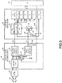
- Fig. 5 is a block diagram illustrating the structures of the power supply unit 20 and the control substrate 30 of an electronic device (image forming apparatus) involved in the second embodiment.
- the electrolytic capacitor 28 serving as a power storage device is replaced by a device 29 which is higher than the electrolytic capacitor 28 in charging capacity and can be charged and discharged.
- the device 29 which can be charged and discharged is, for example, a double electric layer capacitor, a lithium ion battery, a lithium ion capacitor, a nickel-cadmium battery, a nickel-metal hydride battery or a fuel cell.
- the deployment of the device 29 which can be charged and discharged as a power storage device makes the first AC/DC circuit 25 and the second AC/DC circuit 26 in a load-free state in the sleep mode, which prolongs a load-free period and therefore reduces power consumption.
- the voltage of the device 29 which can be charged and discharged is effectively used, thus reducing power consumption.
- the present invention may have various applications, but not limited to the foregoing embodiments.
- the foregoing power supply unit 20 or control substrate 30 may be applied to other electronic devices which function in a normal mode and a sleep mode.
- the units B and D act in the sleep mode, however, other units may act in the sleep mode. That is, the unit acting in a sleep mode is determined matching with the actual circuits of the electronic device, and the second output voltage is supplied to the determined unit.
- the comparator circuit 33 is used as the voltage monitoring unit 32, however, the output voltage V1 may also be monitored by the CPU 101, and the switching circuit 31 is controlled when the output voltage V1 is below a specific threshold in the sleep mode.
Landscapes
- Physics & Mathematics (AREA)
- General Physics & Mathematics (AREA)
- Engineering & Computer Science (AREA)
- Microelectronics & Electronic Packaging (AREA)
- Control Or Security For Electrophotography (AREA)
- Accessory Devices And Overall Control Thereof (AREA)
Claims (10)
- Elektronische Vorrichtung für eine Bildgebungseinrichtung, wobei die elektronische Vorrichtung in der Lage ist, in einem allgemeinen Aktionsmodus und einem Stromsparmodus zu agieren, umfassend:eine Vielzahl von Einheiten (A, C, D, E, F, G), die ausgestaltet sind, in dem gemeinsamen Aktionsmodus zu agieren;eine erste AC/DC-Schaltung (25), die ausgestaltet ist, eine erste Gleichspannung der Vielzahl von den Einheiten zuzuführen;eine Stromspeichervorrichtung (28, 29), die mit der Ausgangsklemme der ersten AC/DC-Schaltung verbunden ist;eine zweite AC/DC-Schaltung (26), die ausgestaltet ist, eine zweite Gleichspannung der spezifischen (B, D) der Einheiten zuzuführen, die in dem Stromsparmodus agiert;einen Schaltkreis (31), der ausgestaltet ist, zwischen einem ersten Zustand (311 EIN), in dem die erste Gleichspannung der Vielzahl von Einheiten in dem allgemeinen Aktionsmodus zugeführt wird, und einem zweiten Zustand (312 EIN), in dem die zweite Gleichspannung der spezifischen Einheit in dem Stromsparmodus zugeführt wird, zu schalten; undeine Steuer- bzw. Regeleinheit (11), die ausgestaltet ist, zwischen dem allgemeinen Aktionsmodus, in dem die erste AC/DC-Schaltung agiert, und dem Stromsparmodus, in dem die erste AC/DC-Schaltung aufhört, zu agieren, zu unterscheiden, und den Schaltkreis entsprechend zu steuern bzw. zu regeln,dadurch gekennzeichnet, dass sie überdieseine Spannungsüberwachungseinheit (32) umfasst, die ausgestaltet ist, den Stromspeicher der Stromspeichervorrichtung zu überwachen; unddass die Steuer- bzw. Regeleinheit (11) angebracht ist, den Schaltkreis zu steuern bzw. zu regeln, um den aktuellen Zustand des Schaltkreises während des Zeitraums, in dem die Spannungsüberwachungseinheit angibt, dass sich der Stromspeicher der Stromspeichervorrichtung vermindert, auf einem voreingestellten Schwellenwert zu halten oder den Schaltkreis in den zweiten Zustand zu schalten, wenn die Spannungsüberwachungseinheit angibt, dass sich der Stromspeicher der Stromspeichervorrichtung vermindert hat, um unterhalb des Schwellenwerts zu liegen, nachdem der allgemeine Aktionsmodus in den Stromsparmodus geschaltet worden ist.
- Elektronische Vorrichtung nach Anspruch 1, wobei die Stromspeichervorrichtung (29) eine Vorrichtung ist, die mit der Ausgangsklemme der ersten AC/DC-Schaltung verbunden ist und geladen und entladen werden kann.
- Elektronische Vorrichtung nach Anspruch 1 oder 2, wobei
die Stromspeichervorrichtung (28) ein elektrolytischer Kondensator zum Stabilisieren der ersten Gleichspannung ist. - Bildgebungseinrichtung, umfassend:eine benutzerbedienbare Steuer- bzw. Regeltafel (14);eine elektronische Vorrichtung nach einem beliebigen der Ansprüche 1 bis 3, wobei die Vielzahl von Einheiten ausgestaltet ist, in dem allgemeinen Aktionsmodus zu agieren, umfasst eine Bildgebungseinheit (F) zum Bilden eines Bilds auf einer Folie.
- Bildgebungseinrichtung nach Anspruch 4, wobei
die Stromspeichervorrichtung (29) eine Vorrichtung ist, die mit der Ausgangsklemme der ersten AC/DC-Schaltung verbunden ist und geladen und entladen werden kann. - Bildgebungseinrichtung nach Anspruch 4 oder 5, wobei
die Stromspeichervorrichtung (28) ein elektrolytischer Kondensator zum Stabilisieren der ersten Gleichspannung ist. - Bildgebungseinrichtung nach einem beliebigen der Ansprüche 4 bis 6, wobei
die Steuer- bzw. Regeleinheit (11) eine Steuerung bzw. Regelung ausführt, um den allgemeinen Aktionsmodus von dem Stromspeichermodus als Reaktion auf den Betrieb der Steuer- bzw. Regeltafel wiederherzustellen. - Bildgebungseinrichtung nach einem beliebigen der Ansprüche 4 bis 7, wobei
die spezifischen Einheiten ein Teil einer CPU sind, die die Steuer- bzw. Regeleinheit (B) und eine Antriebseinheit (D) zum Steuern bzw. Regeln der Aktionen der Steuer- bzw. Regeltafel darstellt. - Stromversorgungssteuerungsverfahren bzw. -regelverfahren für eine elektronische Vorrichtung für eine Bildgebungseinrichtung, wobei die elektronische Vorrichtung in der Lage ist, in einem allgemeinen Aktionsmodus und einem Stromsparmodus zu agieren, umfassend:Erzeugen, mittels einer ersten AC/DC-Schaltung (25), einer ersten Gleichspannung für eine Vielzahl von Einheiten, die in dem allgemeinen Aktionsmodus agieren;Laden einer Stromspeichervorrichtung (28, 29) mit der ersten Gleichspannung;Erzeugen, mittels einer zweiten AC/DC-Schaltung (26), einer zweiten Gleichspannung für die spezifische der Vielzahl von Einheiten, die in dem Stromsparmodus agieren;Schalten eines Schaltkreises (31) zwischen einem ersten Zustand (311 EIN), in dem die erste Gleichspannung der Vielzahl von Einheiten in dem allgemeinen Aktionsmodus zugeführt wird, und einem zweiten Zustand (312 EIN), in dem die zweite Gleichspannung der spezifischen Einheit in dem Stromsparmodus zugeführt wird;
undUnterscheiden, von einer Steuer- bzw. Regeleinheit (11), zwischen dem allgemeinen Aktionsmodus, in dem die erste AC/DC-Schaltung agiert, und dem Stromsparmodus, in dem die erste AC-/DC-Schaltung aufhört, zu agieren, und entsprechendes Steuern bzw. Regeln des Schaltkreises,gekennzeichnet durch folgende Schritte:Überwachen (32) des Stromspeichers (28, 29) der Stromspeichervorrichtung;Dazubringen der Steuer- bzw. Regeleinheit, den Schaltkreis (31) zu steuern bzw. regeln, um den aktuellen Zustand des Schaltkreises während des Zeitraums aufrechtzuerhalten, indem der Stromspeicher der Stromspeichervorrichtung zu einem voreingestellten Schwellenwert vermindert wird, oder Schalten des Schaltkreises in den zweiten Zustand, wenn sich der Stromspeicher der Stromspeichervorrichtung vermindert hat, um unterhalb des Schwellenwerts zu sein, nachdem der allgemeine Aktionsmodus in den Stromsparmodus geschaltet wird. - Stromversorgungssteuerverfahren bzw. -regelverfahren nach Anspruch 9, wobei
die Stromspeichervorrichtung (29) eine Vorrichtung ist, die mit der Ausgangsklemme der ersten AC/DC-Schaltung verbunden ist und mit der ersten Gleichspannung geladen und entladen werden kann.
Priority Applications (1)
| Application Number | Priority Date | Filing Date | Title |
|---|---|---|---|
| EP15179996.2A EP3128372B1 (de) | 2015-08-06 | 2015-08-06 | Elektronische vorrichtung, bilderzeugungsvorrichtung und stromversorgungssteuerungsverfahren für elektronische vorrichtung |
Applications Claiming Priority (1)
| Application Number | Priority Date | Filing Date | Title |
|---|---|---|---|
| EP15179996.2A EP3128372B1 (de) | 2015-08-06 | 2015-08-06 | Elektronische vorrichtung, bilderzeugungsvorrichtung und stromversorgungssteuerungsverfahren für elektronische vorrichtung |
Publications (2)
| Publication Number | Publication Date |
|---|---|
| EP3128372A1 EP3128372A1 (de) | 2017-02-08 |
| EP3128372B1 true EP3128372B1 (de) | 2018-10-03 |
Family
ID=53835304
Family Applications (1)
| Application Number | Title | Priority Date | Filing Date |
|---|---|---|---|
| EP15179996.2A Not-in-force EP3128372B1 (de) | 2015-08-06 | 2015-08-06 | Elektronische vorrichtung, bilderzeugungsvorrichtung und stromversorgungssteuerungsverfahren für elektronische vorrichtung |
Country Status (1)
| Country | Link |
|---|---|
| EP (1) | EP3128372B1 (de) |
Family Cites Families (3)
| Publication number | Priority date | Publication date | Assignee | Title |
|---|---|---|---|---|
| US8901780B2 (en) * | 2010-07-28 | 2014-12-02 | Kabushiki Kaisha Toshiba | Image forming apparatus |
| JP5899959B2 (ja) * | 2012-01-23 | 2016-04-06 | 株式会社リコー | 電源装置、電子機器及び画像形成装置 |
| JP2015068989A (ja) * | 2013-09-30 | 2015-04-13 | 株式会社リコー | 画像形成装置 |
-
2015
- 2015-08-06 EP EP15179996.2A patent/EP3128372B1/de not_active Not-in-force
Non-Patent Citations (1)
| Title |
|---|
| None * |
Also Published As
| Publication number | Publication date |
|---|---|
| EP3128372A1 (de) | 2017-02-08 |
Similar Documents
| Publication | Publication Date | Title |
|---|---|---|
| US10466752B2 (en) | Information processing apparatus that offers chance of eliminating hang-up state, control method therefor, and storage medium | |
| US7966501B2 (en) | Multi-function peripheral, power supply apparatus, and power supply control method | |
| US7539886B2 (en) | Image processing apparatus, power saving control method, and program and storage medium thereof | |
| CN103312046B (zh) | 电力控制系统及电子装置 | |
| US9122187B2 (en) | Charging device, image forming apparatus, and computer program product | |
| US9317091B2 (en) | Electronic device, method of controlling power supply, and recording medium storing power supply control program | |
| US9581950B2 (en) | Image forming apparatus with first and second power supply | |
| JP2015176443A (ja) | 情報処理装置及びその制御方法、並びにプログラム | |
| JP2013168869A (ja) | 電子機器、画像処理装置及び機器制御方法 | |
| CN104113651B (zh) | 处理控制设备、图像处理设备和处理控制方法 | |
| US20150288294A1 (en) | Switching mode power supply | |
| US20130061079A1 (en) | Image processing apparatus, method for controlling the same and storage medium | |
| CN103765344B (zh) | 具备多个显示装置的系统和图像处理装置 | |
| US20200145550A1 (en) | Printing apparatus and control method of the printing apparatus | |
| EP3128372B1 (de) | Elektronische vorrichtung, bilderzeugungsvorrichtung und stromversorgungssteuerungsverfahren für elektronische vorrichtung | |
| KR20150026988A (ko) | 전자 기기, 및 전자 기기의 제어 유닛에의 전력 제어 방법 | |
| CN104253921A (zh) | 图像形成装置 | |
| JP2021108517A (ja) | 電源回路、及び電源回路を備えた電子機器 | |
| EP3128371B1 (de) | Elektronische vorrichtung, bilderzeugungsvorrichtung und stromversorgungssteuerungsverfahren für elektronische vorrichtung | |
| US9008532B2 (en) | Image processing apparatus operable by AC power and DC power, method of controlling the apparatus, and storage medium | |
| JP7596749B2 (ja) | 電源装置、電源装置の制御方法および電源装置の制御プログラム | |
| JP2013054355A (ja) | 画像形成装置、電源切り替え制御方法 | |
| JP4919324B2 (ja) | 画像形成装置、電源供給制御方法及びプログラム | |
| US20200133359A1 (en) | Image forming apparatus | |
| JP6171550B2 (ja) | 電源制御装置及び画像処理装置 |
Legal Events
| Date | Code | Title | Description |
|---|---|---|---|
| PUAI | Public reference made under article 153(3) epc to a published international application that has entered the european phase |
Free format text: ORIGINAL CODE: 0009012 |
|
| STAA | Information on the status of an ep patent application or granted ep patent |
Free format text: STATUS: THE APPLICATION HAS BEEN PUBLISHED |
|
| AK | Designated contracting states |
Kind code of ref document: A1 Designated state(s): AL AT BE BG CH CY CZ DE DK EE ES FI FR GB GR HR HU IE IS IT LI LT LU LV MC MK MT NL NO PL PT RO RS SE SI SK SM TR |
|
| AX | Request for extension of the european patent |
Extension state: BA ME |
|
| STAA | Information on the status of an ep patent application or granted ep patent |
Free format text: STATUS: REQUEST FOR EXAMINATION WAS MADE |
|
| 17P | Request for examination filed |
Effective date: 20170808 |
|
| RBV | Designated contracting states (corrected) |
Designated state(s): AL AT BE BG CH CY CZ DE DK EE ES FI FR GB GR HR HU IE IS IT LI LT LU LV MC MK MT NL NO PL PT RO RS SE SI SK SM TR |
|
| GRAP | Despatch of communication of intention to grant a patent |
Free format text: ORIGINAL CODE: EPIDOSNIGR1 |
|
| STAA | Information on the status of an ep patent application or granted ep patent |
Free format text: STATUS: GRANT OF PATENT IS INTENDED |
|
| INTG | Intention to grant announced |
Effective date: 20180518 |
|
| RAP1 | Party data changed (applicant data changed or rights of an application transferred) |
Owner name: KABUSHIKI KAISHA TOSHIBA Owner name: TOSHIBA TEC KABUSHIKI KAISHA |
|
| GRAS | Grant fee paid |
Free format text: ORIGINAL CODE: EPIDOSNIGR3 |
|
| GRAA | (expected) grant |
Free format text: ORIGINAL CODE: 0009210 |
|
| STAA | Information on the status of an ep patent application or granted ep patent |
Free format text: STATUS: THE PATENT HAS BEEN GRANTED |
|
| AK | Designated contracting states |
Kind code of ref document: B1 Designated state(s): AL AT BE BG CH CY CZ DE DK EE ES FI FR GB GR HR HU IE IS IT LI LT LU LV MC MK MT NL NO PL PT RO RS SE SI SK SM TR |
|
| RAP1 | Party data changed (applicant data changed or rights of an application transferred) |
Owner name: TOSHIBA TEC KABUSHIKI KAISHA Owner name: KABUSHIKI KAISHA TOSHIBA |
|
| REG | Reference to a national code |
Ref country code: GB Ref legal event code: FG4D |
|
| REG | Reference to a national code |
Ref country code: CH Ref legal event code: EP Ref country code: AT Ref legal event code: REF Ref document number: 1049259 Country of ref document: AT Kind code of ref document: T Effective date: 20181015 |
|
| REG | Reference to a national code |
Ref country code: IE Ref legal event code: FG4D Ref country code: DE Ref legal event code: R096 Ref document number: 602015017378 Country of ref document: DE |
|
| REG | Reference to a national code |
Ref country code: NL Ref legal event code: MP Effective date: 20181003 |
|
| REG | Reference to a national code |
Ref country code: LT Ref legal event code: MG4D |
|
| REG | Reference to a national code |
Ref country code: AT Ref legal event code: MK05 Ref document number: 1049259 Country of ref document: AT Kind code of ref document: T Effective date: 20181003 |
|
| PG25 | Lapsed in a contracting state [announced via postgrant information from national office to epo] |
Ref country code: NL Free format text: LAPSE BECAUSE OF FAILURE TO SUBMIT A TRANSLATION OF THE DESCRIPTION OR TO PAY THE FEE WITHIN THE PRESCRIBED TIME-LIMIT Effective date: 20181003 |
|
| PG25 | Lapsed in a contracting state [announced via postgrant information from national office to epo] |
Ref country code: PL Free format text: LAPSE BECAUSE OF FAILURE TO SUBMIT A TRANSLATION OF THE DESCRIPTION OR TO PAY THE FEE WITHIN THE PRESCRIBED TIME-LIMIT Effective date: 20181003 Ref country code: AT Free format text: LAPSE BECAUSE OF FAILURE TO SUBMIT A TRANSLATION OF THE DESCRIPTION OR TO PAY THE FEE WITHIN THE PRESCRIBED TIME-LIMIT Effective date: 20181003 Ref country code: HR Free format text: LAPSE BECAUSE OF FAILURE TO SUBMIT A TRANSLATION OF THE DESCRIPTION OR TO PAY THE FEE WITHIN THE PRESCRIBED TIME-LIMIT Effective date: 20181003 Ref country code: LV Free format text: LAPSE BECAUSE OF FAILURE TO SUBMIT A TRANSLATION OF THE DESCRIPTION OR TO PAY THE FEE WITHIN THE PRESCRIBED TIME-LIMIT Effective date: 20181003 Ref country code: NO Free format text: LAPSE BECAUSE OF FAILURE TO SUBMIT A TRANSLATION OF THE DESCRIPTION OR TO PAY THE FEE WITHIN THE PRESCRIBED TIME-LIMIT Effective date: 20190103 Ref country code: ES Free format text: LAPSE BECAUSE OF FAILURE TO SUBMIT A TRANSLATION OF THE DESCRIPTION OR TO PAY THE FEE WITHIN THE PRESCRIBED TIME-LIMIT Effective date: 20181003 Ref country code: IS Free format text: LAPSE BECAUSE OF FAILURE TO SUBMIT A TRANSLATION OF THE DESCRIPTION OR TO PAY THE FEE WITHIN THE PRESCRIBED TIME-LIMIT Effective date: 20190203 Ref country code: BG Free format text: LAPSE BECAUSE OF FAILURE TO SUBMIT A TRANSLATION OF THE DESCRIPTION OR TO PAY THE FEE WITHIN THE PRESCRIBED TIME-LIMIT Effective date: 20190103 Ref country code: LT Free format text: LAPSE BECAUSE OF FAILURE TO SUBMIT A TRANSLATION OF THE DESCRIPTION OR TO PAY THE FEE WITHIN THE PRESCRIBED TIME-LIMIT Effective date: 20181003 Ref country code: CZ Free format text: LAPSE BECAUSE OF FAILURE TO SUBMIT A TRANSLATION OF THE DESCRIPTION OR TO PAY THE FEE WITHIN THE PRESCRIBED TIME-LIMIT Effective date: 20181003 Ref country code: FI Free format text: LAPSE BECAUSE OF FAILURE TO SUBMIT A TRANSLATION OF THE DESCRIPTION OR TO PAY THE FEE WITHIN THE PRESCRIBED TIME-LIMIT Effective date: 20181003 |
|
| PG25 | Lapsed in a contracting state [announced via postgrant information from national office to epo] |
Ref country code: GR Free format text: LAPSE BECAUSE OF FAILURE TO SUBMIT A TRANSLATION OF THE DESCRIPTION OR TO PAY THE FEE WITHIN THE PRESCRIBED TIME-LIMIT Effective date: 20190104 Ref country code: RS Free format text: LAPSE BECAUSE OF FAILURE TO SUBMIT A TRANSLATION OF THE DESCRIPTION OR TO PAY THE FEE WITHIN THE PRESCRIBED TIME-LIMIT Effective date: 20181003 Ref country code: AL Free format text: LAPSE BECAUSE OF FAILURE TO SUBMIT A TRANSLATION OF THE DESCRIPTION OR TO PAY THE FEE WITHIN THE PRESCRIBED TIME-LIMIT Effective date: 20181003 Ref country code: PT Free format text: LAPSE BECAUSE OF FAILURE TO SUBMIT A TRANSLATION OF THE DESCRIPTION OR TO PAY THE FEE WITHIN THE PRESCRIBED TIME-LIMIT Effective date: 20190203 Ref country code: SE Free format text: LAPSE BECAUSE OF FAILURE TO SUBMIT A TRANSLATION OF THE DESCRIPTION OR TO PAY THE FEE WITHIN THE PRESCRIBED TIME-LIMIT Effective date: 20181003 |
|
| REG | Reference to a national code |
Ref country code: DE Ref legal event code: R097 Ref document number: 602015017378 Country of ref document: DE |
|
| PG25 | Lapsed in a contracting state [announced via postgrant information from national office to epo] |
Ref country code: IT Free format text: LAPSE BECAUSE OF FAILURE TO SUBMIT A TRANSLATION OF THE DESCRIPTION OR TO PAY THE FEE WITHIN THE PRESCRIBED TIME-LIMIT Effective date: 20181003 Ref country code: DK Free format text: LAPSE BECAUSE OF FAILURE TO SUBMIT A TRANSLATION OF THE DESCRIPTION OR TO PAY THE FEE WITHIN THE PRESCRIBED TIME-LIMIT Effective date: 20181003 |
|
| PLBE | No opposition filed within time limit |
Free format text: ORIGINAL CODE: 0009261 |
|
| STAA | Information on the status of an ep patent application or granted ep patent |
Free format text: STATUS: NO OPPOSITION FILED WITHIN TIME LIMIT |
|
| PG25 | Lapsed in a contracting state [announced via postgrant information from national office to epo] |
Ref country code: RO Free format text: LAPSE BECAUSE OF FAILURE TO SUBMIT A TRANSLATION OF THE DESCRIPTION OR TO PAY THE FEE WITHIN THE PRESCRIBED TIME-LIMIT Effective date: 20181003 Ref country code: EE Free format text: LAPSE BECAUSE OF FAILURE TO SUBMIT A TRANSLATION OF THE DESCRIPTION OR TO PAY THE FEE WITHIN THE PRESCRIBED TIME-LIMIT Effective date: 20181003 Ref country code: SM Free format text: LAPSE BECAUSE OF FAILURE TO SUBMIT A TRANSLATION OF THE DESCRIPTION OR TO PAY THE FEE WITHIN THE PRESCRIBED TIME-LIMIT Effective date: 20181003 Ref country code: SK Free format text: LAPSE BECAUSE OF FAILURE TO SUBMIT A TRANSLATION OF THE DESCRIPTION OR TO PAY THE FEE WITHIN THE PRESCRIBED TIME-LIMIT Effective date: 20181003 |
|
| 26N | No opposition filed |
Effective date: 20190704 |
|
| PG25 | Lapsed in a contracting state [announced via postgrant information from national office to epo] |
Ref country code: SI Free format text: LAPSE BECAUSE OF FAILURE TO SUBMIT A TRANSLATION OF THE DESCRIPTION OR TO PAY THE FEE WITHIN THE PRESCRIBED TIME-LIMIT Effective date: 20181003 |
|
| PGFP | Annual fee paid to national office [announced via postgrant information from national office to epo] |
Ref country code: FR Payment date: 20190711 Year of fee payment: 5 Ref country code: DE Payment date: 20190723 Year of fee payment: 5 |
|
| PGFP | Annual fee paid to national office [announced via postgrant information from national office to epo] |
Ref country code: GB Payment date: 20190731 Year of fee payment: 5 |
|
| PG25 | Lapsed in a contracting state [announced via postgrant information from national office to epo] |
Ref country code: TR Free format text: LAPSE BECAUSE OF FAILURE TO SUBMIT A TRANSLATION OF THE DESCRIPTION OR TO PAY THE FEE WITHIN THE PRESCRIBED TIME-LIMIT Effective date: 20181003 |
|
| PG25 | Lapsed in a contracting state [announced via postgrant information from national office to epo] |
Ref country code: LU Free format text: LAPSE BECAUSE OF NON-PAYMENT OF DUE FEES Effective date: 20190806 Ref country code: LI Free format text: LAPSE BECAUSE OF NON-PAYMENT OF DUE FEES Effective date: 20190831 Ref country code: MC Free format text: LAPSE BECAUSE OF FAILURE TO SUBMIT A TRANSLATION OF THE DESCRIPTION OR TO PAY THE FEE WITHIN THE PRESCRIBED TIME-LIMIT Effective date: 20181003 Ref country code: CH Free format text: LAPSE BECAUSE OF NON-PAYMENT OF DUE FEES Effective date: 20190831 |
|
| REG | Reference to a national code |
Ref country code: BE Ref legal event code: MM Effective date: 20190831 |
|
| PG25 | Lapsed in a contracting state [announced via postgrant information from national office to epo] |
Ref country code: IE Free format text: LAPSE BECAUSE OF NON-PAYMENT OF DUE FEES Effective date: 20190806 |
|
| PG25 | Lapsed in a contracting state [announced via postgrant information from national office to epo] |
Ref country code: BE Free format text: LAPSE BECAUSE OF NON-PAYMENT OF DUE FEES Effective date: 20190831 |
|
| REG | Reference to a national code |
Ref country code: DE Ref legal event code: R119 Ref document number: 602015017378 Country of ref document: DE |
|
| GBPC | Gb: european patent ceased through non-payment of renewal fee |
Effective date: 20200806 |
|
| PG25 | Lapsed in a contracting state [announced via postgrant information from national office to epo] |
Ref country code: CY Free format text: LAPSE BECAUSE OF FAILURE TO SUBMIT A TRANSLATION OF THE DESCRIPTION OR TO PAY THE FEE WITHIN THE PRESCRIBED TIME-LIMIT Effective date: 20181003 |
|
| PG25 | Lapsed in a contracting state [announced via postgrant information from national office to epo] |
Ref country code: DE Free format text: LAPSE BECAUSE OF NON-PAYMENT OF DUE FEES Effective date: 20210302 Ref country code: HU Free format text: LAPSE BECAUSE OF FAILURE TO SUBMIT A TRANSLATION OF THE DESCRIPTION OR TO PAY THE FEE WITHIN THE PRESCRIBED TIME-LIMIT; INVALID AB INITIO Effective date: 20150806 Ref country code: MT Free format text: LAPSE BECAUSE OF FAILURE TO SUBMIT A TRANSLATION OF THE DESCRIPTION OR TO PAY THE FEE WITHIN THE PRESCRIBED TIME-LIMIT Effective date: 20181003 Ref country code: FR Free format text: LAPSE BECAUSE OF NON-PAYMENT OF DUE FEES Effective date: 20200831 |
|
| PG25 | Lapsed in a contracting state [announced via postgrant information from national office to epo] |
Ref country code: GB Free format text: LAPSE BECAUSE OF NON-PAYMENT OF DUE FEES Effective date: 20200806 |
|
| PG25 | Lapsed in a contracting state [announced via postgrant information from national office to epo] |
Ref country code: MK Free format text: LAPSE BECAUSE OF FAILURE TO SUBMIT A TRANSLATION OF THE DESCRIPTION OR TO PAY THE FEE WITHIN THE PRESCRIBED TIME-LIMIT Effective date: 20181003 |