EP3127406B1 - Appareil électrique et procédé de production d'un appareil électrique - Google Patents
Appareil électrique et procédé de production d'un appareil électrique Download PDFInfo
- Publication number
- EP3127406B1 EP3127406B1 EP15709414.5A EP15709414A EP3127406B1 EP 3127406 B1 EP3127406 B1 EP 3127406B1 EP 15709414 A EP15709414 A EP 15709414A EP 3127406 B1 EP3127406 B1 EP 3127406B1
- Authority
- EP
- European Patent Office
- Prior art keywords
- circuit board
- printed circuit
- electrical device
- terminal
- screw
- Prior art date
- Legal status (The legal status is an assumption and is not a legal conclusion. Google has not performed a legal analysis and makes no representation as to the accuracy of the status listed.)
- Active
Links
- 238000004519 manufacturing process Methods 0.000 title claims description 8
- 239000003990 capacitor Substances 0.000 claims description 34
- 125000006850 spacer group Chemical group 0.000 claims description 19
- 239000004020 conductor Substances 0.000 claims description 13
- 238000000034 method Methods 0.000 claims description 10
- 239000004033 plastic Substances 0.000 claims description 8
- 229920003023 plastic Polymers 0.000 claims description 8
- 239000002184 metal Substances 0.000 claims description 7
- 239000002131 composite material Substances 0.000 claims description 4
- 239000012777 electrically insulating material Substances 0.000 claims description 2
- 239000000463 material Substances 0.000 claims description 2
- 230000007935 neutral effect Effects 0.000 description 5
- 230000007613 environmental effect Effects 0.000 description 4
- 238000009423 ventilation Methods 0.000 description 4
- 230000015556 catabolic process Effects 0.000 description 2
- 238000010586 diagram Methods 0.000 description 2
- 238000005516 engineering process Methods 0.000 description 2
- 239000011159 matrix material Substances 0.000 description 2
- 239000007769 metal material Substances 0.000 description 2
- 238000005476 soldering Methods 0.000 description 2
- 230000006978 adaptation Effects 0.000 description 1
- 230000007547 defect Effects 0.000 description 1
- 239000003822 epoxy resin Substances 0.000 description 1
- 238000007667 floating Methods 0.000 description 1
- 230000005484 gravity Effects 0.000 description 1
- 238000009413 insulation Methods 0.000 description 1
- 238000013017 mechanical damping Methods 0.000 description 1
- 238000012806 monitoring device Methods 0.000 description 1
- 229920000647 polyepoxide Polymers 0.000 description 1
- 230000001681 protective effect Effects 0.000 description 1
- 239000004065 semiconductor Substances 0.000 description 1
- 239000000758 substrate Substances 0.000 description 1
- 230000001629 suppression Effects 0.000 description 1
Images


Classifications
-
- H—ELECTRICITY
- H05—ELECTRIC TECHNIQUES NOT OTHERWISE PROVIDED FOR
- H05K—PRINTED CIRCUITS; CASINGS OR CONSTRUCTIONAL DETAILS OF ELECTRIC APPARATUS; MANUFACTURE OF ASSEMBLAGES OF ELECTRICAL COMPONENTS
- H05K7/00—Constructional details common to different types of electric apparatus
- H05K7/14—Mounting supporting structure in casing or on frame or rack
- H05K7/1417—Mounting supporting structure in casing or on frame or rack having securing means for mounting boards, plates or wiring boards
- H05K7/142—Spacers not being card guides
-
- H—ELECTRICITY
- H05—ELECTRIC TECHNIQUES NOT OTHERWISE PROVIDED FOR
- H05K—PRINTED CIRCUITS; CASINGS OR CONSTRUCTIONAL DETAILS OF ELECTRIC APPARATUS; MANUFACTURE OF ASSEMBLAGES OF ELECTRICAL COMPONENTS
- H05K7/00—Constructional details common to different types of electric apparatus
- H05K7/14—Mounting supporting structure in casing or on frame or rack
- H05K7/1422—Printed circuit boards receptacles, e.g. stacked structures, electronic circuit modules or box like frames
- H05K7/1427—Housings
- H05K7/1432—Housings specially adapted for power drive units or power converters
- H05K7/14322—Housings specially adapted for power drive units or power converters wherein the control and power circuits of a power converter are arranged within the same casing
-
- H—ELECTRICITY
- H05—ELECTRIC TECHNIQUES NOT OTHERWISE PROVIDED FOR
- H05K—PRINTED CIRCUITS; CASINGS OR CONSTRUCTIONAL DETAILS OF ELECTRIC APPARATUS; MANUFACTURE OF ASSEMBLAGES OF ELECTRICAL COMPONENTS
- H05K1/00—Printed circuits
- H05K1/18—Printed circuits structurally associated with non-printed electric components
- H05K1/182—Printed circuits structurally associated with non-printed electric components associated with components mounted in the printed circuit board, e.g. insert mounted components [IMC]
-
- H—ELECTRICITY
- H05—ELECTRIC TECHNIQUES NOT OTHERWISE PROVIDED FOR
- H05K—PRINTED CIRCUITS; CASINGS OR CONSTRUCTIONAL DETAILS OF ELECTRIC APPARATUS; MANUFACTURE OF ASSEMBLAGES OF ELECTRICAL COMPONENTS
- H05K5/00—Casings, cabinets or drawers for electric apparatus
- H05K5/0026—Casings, cabinets or drawers for electric apparatus provided with connectors and printed circuit boards [PCB], e.g. automotive electronic control units
- H05K5/0069—Casings, cabinets or drawers for electric apparatus provided with connectors and printed circuit boards [PCB], e.g. automotive electronic control units having connector relating features for connecting the connector pins with the PCB or for mounting the connector body with the housing
-
- H—ELECTRICITY
- H05—ELECTRIC TECHNIQUES NOT OTHERWISE PROVIDED FOR
- H05K—PRINTED CIRCUITS; CASINGS OR CONSTRUCTIONAL DETAILS OF ELECTRIC APPARATUS; MANUFACTURE OF ASSEMBLAGES OF ELECTRICAL COMPONENTS
- H05K7/00—Constructional details common to different types of electric apparatus
- H05K7/14—Mounting supporting structure in casing or on frame or rack
- H05K7/1422—Printed circuit boards receptacles, e.g. stacked structures, electronic circuit modules or box like frames
- H05K7/1427—Housings
- H05K7/1432—Housings specially adapted for power drive units or power converters
-
- H—ELECTRICITY
- H02—GENERATION; CONVERSION OR DISTRIBUTION OF ELECTRIC POWER
- H02K—DYNAMO-ELECTRIC MACHINES
- H02K11/00—Structural association of dynamo-electric machines with electric components or with devices for shielding, monitoring or protection
- H02K11/30—Structural association with control circuits or drive circuits
- H02K11/33—Drive circuits, e.g. power electronics
-
- H—ELECTRICITY
- H02—GENERATION; CONVERSION OR DISTRIBUTION OF ELECTRIC POWER
- H02M—APPARATUS FOR CONVERSION BETWEEN AC AND AC, BETWEEN AC AND DC, OR BETWEEN DC AND DC, AND FOR USE WITH MAINS OR SIMILAR POWER SUPPLY SYSTEMS; CONVERSION OF DC OR AC INPUT POWER INTO SURGE OUTPUT POWER; CONTROL OR REGULATION THEREOF
- H02M7/00—Conversion of ac power input into dc power output; Conversion of dc power input into ac power output
- H02M7/003—Constructional details, e.g. physical layout, assembly, wiring or busbar connections
-
- H—ELECTRICITY
- H02—GENERATION; CONVERSION OR DISTRIBUTION OF ELECTRIC POWER
- H02P—CONTROL OR REGULATION OF ELECTRIC MOTORS, ELECTRIC GENERATORS OR DYNAMO-ELECTRIC CONVERTERS; CONTROLLING TRANSFORMERS, REACTORS OR CHOKE COILS
- H02P27/00—Arrangements or methods for the control of AC motors characterised by the kind of supply voltage
- H02P27/04—Arrangements or methods for the control of AC motors characterised by the kind of supply voltage using variable-frequency supply voltage, e.g. inverter or converter supply voltage
- H02P27/06—Arrangements or methods for the control of AC motors characterised by the kind of supply voltage using variable-frequency supply voltage, e.g. inverter or converter supply voltage using dc to ac converters or inverters
-
- H—ELECTRICITY
- H05—ELECTRIC TECHNIQUES NOT OTHERWISE PROVIDED FOR
- H05K—PRINTED CIRCUITS; CASINGS OR CONSTRUCTIONAL DETAILS OF ELECTRIC APPARATUS; MANUFACTURE OF ASSEMBLAGES OF ELECTRICAL COMPONENTS
- H05K2201/00—Indexing scheme relating to printed circuits covered by H05K1/00
- H05K2201/10—Details of components or other objects attached to or integrated in a printed circuit board
- H05K2201/10007—Types of components
- H05K2201/10015—Non-printed capacitor
Definitions
- the invention relates to an electrical device and a method for producing an electrical device.
- the DE 10 2007 012 818 A1 Fig. 10 shows a semiconductor device with terminals.
- the US 2009/0251843 A1 Fig. 13 shows a vehicle-mounted electrical device and a vehicle in which the electrical device is mounted.
- Fig. 13 is an arrangement for effecting basic interference suppression of a matrix converter.
- the invention is therefore based on the object of developing an electrical device and a method for producing an electrical device, the aim being to improve safety.
- the object is achieved in the electrical device according to the features specified in claim 1 and in the method for producing an electrical device according to the features specified in claim 13.
- connection part has a spacing section and a connecting section, wherein the circuit board is spaced apart from the housing part by means of the spacing section, wherein the connecting portion has a threaded portion, in particular wherein the connecting section is connected in an electrically conductive manner to at least one conductor track on the circuit board.
- connection part can be securely connected to the circuit board.
- connection part can be fitted with further components on the circuit board in one work step and can be soldered to the circuit board with the further components in a further work step.
- environmental protection is improved.
- the printed circuit board and the electrical components fitted on the printed circuit board can advantageously be spaced apart from the housing part by means of the spacing section. So the Dielectric strength of the electrical device improved. Voltage flashovers from the electrical components to the housing part can be avoided.
- connection part is designed as a composite part, the connection section being made of an electrically conductive material, in particular made of metal, the spacing section being made of an electrically insulating material, in particular made of plastic.
- the connecting part can be soldered to the printed circuit board in a simple manner by means of the connecting section.
- the printed circuit board and electrical components fitted on the printed circuit board can be spaced apart from the housing part by means of the spacing section, which is designed to be electrically insulating.
- an air gap between the circuit board with the electrical components and the housing part can be specified. The safety of the electrical appliance is improved.
- the spacer section is designed as a plastic injection-molded part.
- the advantage here is that the spacing section can be produced inexpensively in a simple manner.
- the spacer section is molded onto the connecting section.
- the advantage here is that the spacing section can be securely connected to the connecting section in a simple manner.
- the spacing section can advantageously be produced and connected to the connecting section in a single work step.
- the connecting section is at least partially covered by the spacing section. It is advantageous that the spacing section at least partially surrounds the connecting section. As a result, the connection of the spacing section to the connecting section can be implemented in a mechanically stable and secure manner.
- the spacing section engages around an edge, in particular a sheet metal edge, of the connecting section. It is advantageous here that the spacing section at least partially surrounds the edge of the connecting section. The mechanical stability and the security of the connection of the spacing section to the connecting section are thus improved.
- the circuit board is equipped with electrical components, the spacing section being arranged between the circuit board and the housing part in such a way that the electrical components on the circuit board have a minimum distance from the housing part.
- the advantage here is that the dielectric strength of the electrical device is improved. Thus, the safety of the electrical appliance is improved.
- the distance between the electrical components and the housing part is greater than 5 mm.
- the advantage here is that the breakdown voltage of the electrical device is greater than 10 kV. This enables safe operation of the electrical device even at high operating voltages.
- the connecting section has at least one connecting section, in particular a connecting foot, at least one support section and the threaded section.
- the advantage here is that the connecting section can be made compact.
- the connecting section is made in one piece.
- the advantage here is that the connecting section can be manufactured inexpensively. Components can be saved, so environmental protection is improved.
- the connecting section is designed as a stamped and bent part, in particular as a stamped and bent sheet metal part.
- the advantage here is that the connecting section can be manufactured in a simple manner.
- connection section protrudes through a bore in the circuit board and is soldered to a conductor track of the circuit board.
- connection part can be soldered to the circuit board in the same work step as the electrical components fitted on the circuit board.
- the vertical projection of the support section in the circuit board plane surrounds the vertical projection of the bore in the circuit board plane at an angle in the circumferential direction of the projection of the bore of more than 180 °, in particular more than 230 °.
- the advantage here is that the connection part can be arranged on the printed circuit board so that it does not tip over. The safety when soldering the connection section is improved, since the connection section or the connection sections are securely arranged in the bore or the bores. The risk of a soldering defect can be reduced.
- the support section extends perpendicular to a normal vector of the circuit board plane of the circuit board.
- the advantage here is that the connection part can be arranged on the printed circuit board so that it does not tip over.
- the connection part has a large surface facing the circuit board.
- the surface of the support section facing the printed circuit board is advantageously at least 30% of the total surface of the support section, in particular 40%.
- connection part soldered to the circuit board can be prevented from breaking out.
- the housing part has recesses punched through the housing part, a screw part can be passed through one of the recesses and / or the threaded section is arranged in alignment with the recess, the housing part and the connecting section being connectable in an electrically conductive manner by means of the screw part.
- electrical components on the circuit board can be connected to the earth potential by means of the screw part. This enables an optional connection to the earth potential.
- the electrical device can advantageously be adapted to various applications that require different low-voltage networks for electrical power supply.
- an IT system that is designed as a floating network
- the electrical device is used without a screw part, since the electrical components on the circuit board must be isolated from the earthed housing part.
- IT systems are used in small networks with small dimensions and high demands on fail-safe security, for example in hospitals. Additional protective measures are required for personal protection, such as insulation monitoring devices, Overcurrent protection devices, residual current protection devices and / or fault voltage protection devices.
- low-voltage networks with a neutral conductor such as TN systems or TT systems
- the electrical components are partially connected to the earth potential. This makes it easier to detect residual currents than in an IT system, for example using residual current circuit breakers.
- the low-voltage networks with neutral conductors can therefore be designed much larger than the IT system.
- the recess for the screw part can advantageously be produced in one work step with the further recesses, for example ventilation holes.
- the electrical components can advantageously be connected to the grounded housing part by means of the screw part.
- the electrical device can therefore be used for networks with a neutral conductor as well as for networks without a neutral conductor.
- the adaptation to the respective network takes place in a simple manner by screwing the screw part into the connection part or loosening and removing the screw part.
- the housing part functions as a ground connection.
- the advantage here is that the electrical device can be made compact. Components can be saved. Environmental protection is improved.
- a screw part is passed through a recess in the housing part and screw-connected to the threaded section, in particular this screw connection being designed to be self-locking, the screw part connecting the housing part and the connecting section in an electrically conductive manner.
- a perforated disk is arranged between a screw head of the screw part and the housing part.
- the spacer section has a recess through which the screw part can be passed, in particular passed through.
- the advantage here is that the spacer section can be clamped between the housing part and the connecting section. The contact pressure of the screw part can be evenly distributed over the spacing section that partially surrounds the screw part.
- the elastically designed spacer section advantageously functions as a mechanical damping means against vibrations of the housing part.
- the vibrations of the housing part are dampened and the circuit board is arranged in the housing in a vibration-damped manner.
- the recess extends through the spacing section.
- the spacer section is essentially U-shaped, with a region of the screw part being able to be arranged, in particular arranged, between the legs of the U.
- first capacitors are fitted on the printed circuit board, the first capacitors having a common star point, the star point being connected in an electrically conductive manner to the connecting section of the connection part, in particular by means of conductor tracks.
- the star point is grounded by means of the connection part.
- the advantage here is that the grounding can be carried out in a simple and stable manner.
- first capacitors are fitted on the printed circuit board, the first capacitances having a common star point, the star point being electrical is conductively connected to a fourth capacitance, the fourth capacitance being connected to the connecting section of the connection part, in particular by means of at least one conductor track of the circuit board, the fourth capacitance being arranged electrically between the star point and the connection part, in particular the star point being the fourth capacitance and the connector form a series circuit.
- the fourth capacitance functions as an additional filter, by means of which high-frequency interference currents can be diverted. The tension stability is improved. Thus, the safety of the electrical appliance is improved.
- the fourth capacitance is grounded by means of the connection part.
- second capacitances are fitted on the printed circuit board, the second capacitances forming a series circuit which has a center tap, in particular the center tap being electrically conductively connected to the star point.
- the second capacitances are connected in parallel to a third capacitance, in particular an intermediate circuit capacitor of the converter.
- a third capacitance in particular an intermediate circuit capacitor of the converter.
- the electrical device has a polyphase AC voltage connection on the input side, which has a connection means for each phase, the AC voltage connection feeding a rectifier, with a respective connection means being connected to a respective input pole of the rectifier by means of a respective phase line, each phase line in each case having a tap, a first capacitance being electrically arranged between each tap and the star point.
- the advantage here is that the first capacities act as a filter system for the electrical device. By means of the first capacitances, high-frequency fault currents can be derived to the star point. Thus, the security is improved.
- the electrical device has an inverter, a voltage intermediate circuit with the third capacitance as an intermediate circuit capacitor being arranged between the rectifier and the inverter, in particular wherein the inverter is fed from the third capacitance.
- the electrical device can be implemented as a converter. An electric motor can be fed by means of the converter, the rotational frequency of which can be set by means of the converter.
- a respective first inductance is arranged in each phase line between the respective connection means and the respective tap for the respective first capacitance.
- a respective second inductance is arranged in each phase line between the respective tap for the respective first capacitance and the respective input pole of the rectifier.
- an electrical device series which has at least two variants of electrical devices are that optionally a first or a second variant is produced, wherein in a first method step a circuit board is equipped with at least one connection part and capacitors, wherein the capacitors have a common star point, in particular to which the connection part is connected in an electrically conductive manner, wherein in a second process step the circuit board is arranged in a grounded housing with a housing part, wherein the star point is electrically isolated from the earthed housing during the production of the first variant, wherein, in an optional third method step for producing the second variant, the star point is electrically conductively connected to the grounded housing by passing a connecting means, in particular a screw part, through a recess in the housing part and releasably connecting it to the connection part.
- a connecting means in particular a screw part
- the advantage here is that the electrical device can be easily adapted to operate in ungrounded low-voltage networks or in low-voltage networks with a neutral conductor.
- connection of electrical components to the grounded housing part can advantageously be carried out in a detachable manner.
- the electrical device can therefore be retrofitted for operation in other types of low-voltage networks.
- the screw part is screwed into the connection part in the third method step.
- the advantage here is that the screw part can be connected to and released from the connecting part in a simple manner.
- the screw connection can advantageously be designed to be self-locking.
- the screw part can thus be connected to the connecting part in a vibration-proof manner.
- the screw part is electrically conductively connected to the grounded housing part, in particular wherein the screw part touches the housing part.
- the advantage here is that the screw part functions as an electrical connection means.
- the screw part advantageously has a lower electrical resistance than Cable connections. This enables a low-resistance connection between the grounded housing part and the connection part. So security is improved.
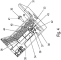
- FIG 4 is a detailed view of the electrical device according to the invention in the second variant drawn in an oblique view, wherein a screw part is shown exploded.
- FIG. 1 The schematic diagram shown shows the electrical device, preferably a converter, with a three-phase AC voltage connection 1, a rectifier 5 and an inverter 8.
- the AC voltage connection 1 has three connection means.
- An inductance (2, 3, 4) is arranged in series with each connection means.
- the rectifier 5 has input poles assigned to the respective phases of the alternating current.
- each phase has a phase line.
- each phase has a branch which is connected to a first capacitance (14, 19, 20).
- the capacitors (14, 19, 20) are connected to a common star point 18.
- the star point 18 can be connected to an earth connection by means of an intermediate connecting means 16.
- a fourth capacitor 15 is arranged between the connecting means 16 and the star point 18.
- a series connection of second capacitances (6, 13) is arranged connected in parallel with a third capacitance 11.
- the second capacitances (6, 13) and the third capacitance 11 are therefore arranged in the DC voltage intermediate circuit.
- the third capacitance 11 is also referred to as an intermediate circuit capacitor.
- the components of the converter are arranged in a housing 10.
- the housing 10 is designed to be at least partially electrically conductive; the housing 10 is preferably made of a metallic material.
- the housing 10 is electrically conductively connected to a ground connection 12 and is therefore grounded.
- the inverter 8 is connected on the output side to a consumer, preferably the consumer is a motor M.
- the consumer has a housing that is electrically connected to a ground connection 9, so the housing of the consumer is grounded.
- FIG. 2 and 4th a detailed view of the second variant of the converter is shown.
- a printed circuit board 38 of the converter is equipped with capacitors (34, 35, 36) which act as capacitors (14, 15, 19, 20).
- the assembled printed circuit board 38 is arranged in a housing which has at least two housing parts (31, 32).
- the housing part 32 has at least one recess, in particular a bore, through which a screw part 30 is passed.
- a perforated disk 41 is preferably arranged on the screw part 30 between the housing part 32 and a screw head of the screw part 30.
- the housing part 32 has further recesses 44 for ventilating the converter, that is to say in particular ventilation holes. These recesses 44 are at least partially arranged in one plane with the recess for the screw part 30.
- the housing part 32 is preferably designed as a stamped and bent part, so that the recess for the screw part 30 and the recesses 44 for ventilation can be produced in one work step.
- the recesses 44 can therefore be punched.
- connection part 40 for the electrically conductive connection of at least one conductor track connected to the capacitors (34, 35, 36) to the housing part 32 is fitted on the circuit board 38.
- the connection part 40 thus has at least one connection section 39 which is inserted into a bore in the circuit board 38, is soldered and / or is connected in an electrically conductive manner to the conductor track.
- the connection part 40 preferably has two connection sections 39.
- connection part 40 has a threaded section 43 into which the screw part 30 is screwed.
- the connection part 40 has a support section 37.
- This support section 37 extends perpendicular to the normal vector of the circuit board plane of the circuit board 38 from an edge region of the circuit board 38 into the circuit board 38.
- the support section 37 is preferably designed in a U-shape.
- the connection section 39 is preferably arranged between the legs of the U-shaped support section 37. The connection section 39 extends from the support section 37.
- the vertical projection of the support section 37 into the circuit board plane surrounds the vertical projection of the bore into the circuit board plane at an angle in the circumferential direction of the projection of the bore of more than 180 °, in particular more than 230 °. This angle is the circumferential angle to the center of gravity of the hole in the circuit board 38.
- the circuit board 38 is designed to be flat and has epoxy resin.
- the plane of the printed circuit board to be that plane which the printed circuit board 38 has when the printed circuit board thickness is vanishing.
- connection part 40 has a one-piece connecting section 42 which has the threaded section 43, the connection section 39 and the support section 37.
- the connecting section 42 is designed as a stamped and bent part, preferably designed as a stamped and bent sheet metal part.
- the connecting section 42 is preferably made of metallic material. The connecting section 42 is thus designed to be electrically conductive.
- the connecting section 42 has a recess in which a threaded sleeve is received, in particular welded or soldered.
- the threaded sleeve has an internal thread for connection to the screw part 30.
- the connection part 40 has a spacing section 33.
- the spacing section 33 separates the housing part 32 from the connecting section 42.
- the spacing section 33 is designed to be electrically insulating.
- the spacing section 33 is preferably made of plastic, in particular as a plastic injection-molded part.
- the plastic is preferably injected onto the connecting section 42.
- the connection part 40 is a composite part, preferably a composite part made of plastic and metal.
- the spacing section 33 has a recess through which the screw part 30 can be passed. This recess is designed as a continuous recess and extends from the threaded section 43 to the housing part 32.
- the spacing section 33 is preferably designed in a U-shape.
- a section of the screw part 30, preferably a threaded section, is preferably arranged between the legs of the U.
- the distance between the connecting section 42 and the housing part 32 is at least as large as the air gap between the assembled printed circuit board 38 and the housing part 32.
- the spacing section 33 thus improves the dielectric strength of the converter.
- the distance caused by the spacing section 33 between the populated circuit board 38 and the housing part 32, ie the air gap, is preferably at least 5 mm, which corresponds to a breakdown voltage of at least 10 kV.
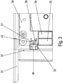
- Figure 3 shows a detailed view of the first variant of the converter.
- connection part 40 is fitted on the circuit board 38.
- the connecting section 42 is arranged to be electrically insulated from the housing part 32.
- the spacer section 33 functions as an insulating means.
- the spacing section 33 is preferably arranged at a distance from the housing part 32.
- the air gap between the spacing section 33 and the housing part 32 is smaller than 1 mm, preferably smaller than 0.5 mm.
- the converter therefore has no connecting means, in particular screw part 30, that connects housing part 32 and connecting part 40 to one another in an electrically conductive manner.
- the recess for the screw part 30 functions as a ventilation hole for the converter.
- connection part 40 is connected to the circuit board 38 using SMD technology by means of surface technology.
- the support section 37 of the connecting part 40 simultaneously functions as a connecting section 42.
Landscapes
- Engineering & Computer Science (AREA)
- Microelectronics & Electronic Packaging (AREA)
- Mounting Of Printed Circuit Boards And The Like (AREA)
- Inverter Devices (AREA)
- Connections Arranged To Contact A Plurality Of Conductors (AREA)
Claims (14)
- Appareil électrique, en particulier convertisseur, comprenant une carte de circuit imprimé (38) et un élément de boîtier (32),
un élément de connexion (40) étant monté, en particulier étant soudé, sur la carte de circuit imprimé (38), l'élément de connexion (40) comportant une portion d'espacement (33) et une portion de liaison (42),
la carte de circuit imprimé (38) étant espacée de l'élément de boîtier (32) au moyen de la portion d'espacement (33),
la portion de liaison (42) comportant une portion filetée (43),
la portion de liaison (42) étant reliée électriquement à au moins une piste conductrice de la carte de circuit imprimé (38),
caractérisé en ce que
des premiers éléments capacitifs (14, 19, 20) sont montés sur la carte de circuit imprimé (38),
les premiers éléments capacitifs (14, 19, 20) comportant un point neutre commun (18),
le point neutre (18) étant relié électriquement à la portion de liaison (42) de l'élément de connexion (40) au moyen de pistes conductrices,
ou
le point neutre (18) étant relié électriquement à un quatrième élément capacitif (15),
le quatrième élément capacitif (15) étant relié à la portion de liaison (42) de l'élément de connexion (40), le quatrième élément capacitif (15) étant disposé électriquement entre le point neutre (18) et l'élément de connexion (40),
l'élément de boîtier comportant un évidement traversant (44),
un élément de vissage (30) pouvant être passé à travers l'évidement (44) et pouvant être vissé sur la portion filetée (43),
l'élément de boîtier (32) et la portion de liaison (42) pouvant être reliés électriquement au moyen de l'élément de vissage (30),
en particulier l'élément de boîtier (32) fonctionnant comme une connexion à la terre (17). - Appareil électrique selon la revendication 1,
caractérisé en ce que
l'élément de connexion (40) est conçu comme un élément composite,
la portion de liaison (42) étant en un matériau électriquement conducteur, en particulier en métal,
la portion d'espacement (33) étant réalisée en un matériau électriquement isolant, en particulier en matière synthétique. - Appareil électrique selon l'une au moins des revendications précédentes,
caractérisé en ce que
la portion d'espacement (33) est conçue comme un élément moulé par injection de matière synthétique,
en particulier la portion d'espacement (33) étant moulée sur la portion de liaison (42),
en particulier la portion de liaison (42) étant au moins partiellement recouverte par la portion d'espacement (33) et/ou la portion d'espacement (33) s'engageant autour d'un bord, en particulier d'un bord de tôle, de la portion de liaison (42). - Appareil électrique selon l'une au moins des revendications précédentes,
caractérisé en ce que
la carte de circuit imprimé (38) est équipée de composants électriques,
la portion d'espacement (33) étant disposée entre la carte de circuit imprimé (38) et l'élément de boîtier (32) de telle sorte que les composants électriques sur la carte de circuit imprimé (38) soient à une distance minimale de l'élément de boîtier (32),
en particulier la distance entre les composants électriques et l'élément de boîtier (32), donc l'espace d'air, étant supérieure à 5 mm. - Appareil électrique selon l'une au moins des revendications précédentes,
caractérisé en ce que
la portion de liaison (42) comporte- au moins une portion de connexion (39), notamment un pied de connexion,- au moins une portion d'appui (37) et- la portion filetée (43),en particulier la portion de liaison (42) étant réalisée d'une seule pièce,
en particulier la portion de liaison (42) étant réalisée sous la forme d'un élément embouti et plié, en particulier sous la forme d'un élément en tôle embouti et plié. - Appareil électrique selon l'une au moins des revendications précédentes,
caractérisé en ce que
une ou la portion de liaison (39) fait saillie à travers un alésage ménagé dans la carte de circuit imprimé (38) et est soudée à une piste conductrice de la carte de circuit imprimé (38),
en particulier la projection verticale de la portion d'appui (39) dans le plan de la carte de circuit imprimé entourant la projection verticale de l'alésage dans le plan de la carte de circuit en formant dans la direction circonférentielle de la projection de l'alésage un angle de plus de 180°, en particulier de plus de 230°,
et/ou en ce que
la portion d'appui (37) s'étend perpendiculairement à un vecteur normal du plan de la carte de circuit imprimé (38) . - Appareil électrique selon l'une au moins des revendications précédentes,
caractérisé en ce que
la portion de vissage (30) passe à travers l'évidement (44) de l'élément de boîtier (32) et est vissée à la portion filetée (43), cette liaison par vissage étant conçue pour être autobloquante,
la portion de vissage (30) reliant électriquement l'élément de boîtier (32) et la portion de liaison (42), en particulier l'élément de boîtier (32) fonctionnant comme une connexion à la terre (17),
en particulier un disque perforé (41) étant disposé entre une tête de vis de l'élément de vissage (30) et l'élément de boîtier (32). - Appareil électrique selon l'une au moins des revendications précédentes,
caractérisé en ce que
la portion d'espacement (33) comporte un évidement à travers lequel l'élément de vissage (30) peut être passé, en particulier est passé,
en particulier l'évidement s'étendant à travers la portion d'espacement (33),
en particulier la portion d'espacement (33) étant sensiblement en forme de U, une région de l'élément de vissage (30) pouvant être disposée, en particulier étant disposée, entre les branches du U. - Appareil électrique selon l'une au moins des revendications précédentes,
caractérisé en ce que
le point neutre (18) est mis à la terre au moyen de l'élément de connexion (40),
ou en ce que
le quatrième élément capacitif (15) est mis à la terre au moyen de l'élément de connexion (40). - Appareil électrique selon l'une au moins des revendications précédentes,
caractérisé en ce que
des deuxièmes éléments capacitifs (6, 13) sont montés sur la carte de circuit imprimé (38),
les deuxièmes éléments capacitifs (6, 13) formant un circuit série qui comporte une prise médiane (7),
en particulier la prise médiane (7) étant reliée électriquement au point neutre (18),
et/ou en ce que
les deuxièmes éléments capacitifs (6, 13) sont montés en parallèle à un troisième élément capacitif (11), en particulier un condensateur de circuit intermédiaire du convertisseur. - Appareil électrique selon l'une au moins des revendications précédentes,
caractérisé en ce que
l'appareil électrique comporte une borne de tension alternative polyphasée côté entrée (1) qui comporte un moyen de connexion pour chaque phase,
la borne de tension alternative (1) alimentant un redresseur (5),
le moyen de connexion respectif étant relié à un pôle d'entrée respectif du redresseur (5) à l'aide d'une ligne de phase respective,
chaque ligne de phase comportant une prise,
un premier élément capacitif (15) étant disposé électriquement entre chaque prise et le point neutre (18) . - Appareil électrique selon l'une au moins des revendications précédentes,
caractérisé en ce que
l'appareil électrique comporte un onduleur (8),
un circuit intermédiaire de tension pourvu du troisième élément capacitif (11) comme condensateur de circuit intermédiaire étant disposé entre le redresseur (5) et l'onduleur (8), en particulier l'onduleur (8) étant alimenté à partir du troisième élément capacitif (11), et/ou en ce que
une première inductance respective (2, 3, 4) est disposée dans chaque ligne de phase entre le moyen de connexion respectif et la prise respective pour le premier élément capacitif respectif (14, 19, 20),
et/ou en ce que
une deuxième inductance respective est disposée dans chaque ligne de phase entre la prise respective destinée au premier élément capacitif respectif (14, 19, 20) et le pôle d'entrée respectif du redresseur (5). - Procédé de production d'un appareil électrique selon l'une au moins des revendications précédentes, d'une série d'appareils électriques comportant au moins deux variantes d'appareils électriques,
caractérisé en ce que
une première ou une deuxième variante est produite au choix,
dans une première étape de procédé une carte de circuit imprimé (38) étant équipée d'au moins un élément de connexion (40) et de condensateurs (34, 35, 36) fonctionnant comme des éléments capacitifs (14, 15, 19, 20),
les condensateurs (34, 35, 36) comportant un point neutre commun (18), en particulier auquel l'élément de connexion (40) est relié électriquement,
dans une deuxième étape de procédé la carte de circuit imprimé (38) étant disposée dans un boîtier, mis à la terre (10), pourvu d'un élément de boîtier (32),
le point neutre (18) étant isolé électriquement du boîtier (10) mis à la terre pendant la production de la première variante,
dans une troisième étape de procédé optionnelle de production de la deuxième variante le point neutre (18) étant relié électriquement au boîtier (10) mis à la terre du fait qu'un moyen de liaison, en particulier un élément de vissage (30), est passé à travers un évidement ménagé dans l'élément de boîtier (32) et est relié de manière amovible à l'élément de connexion (40). - Procédé selon la revendication 13,
caractérisé en ce que
dans la troisième étape de procédé l'élément de vissage (30) est vissé dans l'élément de connexion (40),
en particulier l'élément de vissage (30) étant relié électriquement à l'élément de boîtier (32) mis à la terre, en particulier l'élément de vissage (30) étant en contact avec l'élément de boîtier (32).
Applications Claiming Priority (2)
| Application Number | Priority Date | Filing Date | Title |
|---|---|---|---|
| DE102014004799.7A DE102014004799B4 (de) | 2014-04-03 | 2014-04-03 | Elektrogerät und Verfahren zur Herstellung eines Elektrogerätes |
| PCT/EP2015/000502 WO2015149907A1 (fr) | 2014-04-03 | 2015-03-06 | Appareil électrique et procédé de production d'un appareil électrique |
Publications (2)
| Publication Number | Publication Date |
|---|---|
| EP3127406A1 EP3127406A1 (fr) | 2017-02-08 |
| EP3127406B1 true EP3127406B1 (fr) | 2021-02-24 |
Family
ID=52669574
Family Applications (1)
| Application Number | Title | Priority Date | Filing Date |
|---|---|---|---|
| EP15709414.5A Active EP3127406B1 (fr) | 2014-04-03 | 2015-03-06 | Appareil électrique et procédé de production d'un appareil électrique |
Country Status (6)
| Country | Link |
|---|---|
| US (1) | US10076052B2 (fr) |
| EP (1) | EP3127406B1 (fr) |
| CN (1) | CN106165555B (fr) |
| AU (1) | AU2015240092B2 (fr) |
| DE (1) | DE102014004799B4 (fr) |
| WO (1) | WO2015149907A1 (fr) |
Families Citing this family (5)
| Publication number | Priority date | Publication date | Assignee | Title |
|---|---|---|---|---|
| DE102014010979B3 (de) * | 2014-07-29 | 2015-11-05 | Sew-Eurodrive Gmbh & Co Kg | Verwendung eines Anzeigemittels eines Umrichters, Verfahren zum Betreiben eines Umrichters und Umrichter |
| FR3071695B1 (fr) * | 2017-09-27 | 2021-10-22 | Valeo Japan Co Ltd | Compresseur pour installation de conditionnement d'air pour vehicule automobile |
| CN109659923A (zh) * | 2018-12-20 | 2019-04-19 | 威创集团股份有限公司 | 一种用于电子电气设备的接地结构及电子电气设备 |
| DE102021005368A1 (de) | 2020-11-18 | 2022-05-19 | Sew-Eurodrive Gmbh & Co Kg | Elektrogerät und Anordnung von Elektrogeräten |
| DE102021214906A1 (de) | 2021-10-14 | 2023-04-20 | Vitesco Technologies Germany Gmbh | Elektronische Baugruppe |
Citations (4)
| Publication number | Priority date | Publication date | Assignee | Title |
|---|---|---|---|---|
| EP1069673A1 (fr) * | 1999-07-16 | 2001-01-17 | Schaffner Emv Ag | Filtre réseau |
| US20030179594A1 (en) * | 2000-08-16 | 2003-09-25 | Manfred Bruckmann | Device for effecting the basic interference suppression of a matrix converter |
| EP2416484A2 (fr) * | 2010-07-20 | 2012-02-08 | Kabushiki Kaisha Yaskawa Denki | Convertisseur de matrices |
| DE102012005622A1 (de) * | 2012-03-22 | 2013-09-26 | Sew-Eurodrive Gmbh & Co. Kg | Schaltungsanordnung und Anordnung von Kondensatoren |
Family Cites Families (18)
| Publication number | Priority date | Publication date | Assignee | Title |
|---|---|---|---|---|
| US4254301A (en) * | 1979-03-19 | 1981-03-03 | Xerox Corporation | Printed circuit board component mounting support and spacer |
| US5008777A (en) * | 1988-10-14 | 1991-04-16 | At&T Bell Laboratories | Auxiliary board spacer arrangement |
| JP2933845B2 (ja) | 1995-02-17 | 1999-08-16 | 三菱電機株式会社 | 印刷回路基板取付装置 |
| US6186800B1 (en) * | 1999-01-13 | 2001-02-13 | Micron Electronics, Inc. | Circuit board grounding and support structure |
| US6863562B1 (en) * | 2003-08-21 | 2005-03-08 | International Business Machines Corporation | Pin mounted circuit board retainer |
| US7667299B2 (en) * | 2004-01-27 | 2010-02-23 | Panasonic Corporation | Circuit board and method for mounting chip component |
| JP2005216884A (ja) * | 2004-01-27 | 2005-08-11 | Matsushita Electric Ind Co Ltd | 回路基板およびチップ部品実装方法 |
| JP4577276B2 (ja) * | 2006-06-07 | 2010-11-10 | トヨタ自動車株式会社 | 車載用電子装置およびそれを搭載する車両 |
| JP4242401B2 (ja) * | 2006-06-29 | 2009-03-25 | 三菱電機株式会社 | 半導体装置 |
| WO2009069308A1 (fr) * | 2007-11-30 | 2009-06-04 | Panasonic Corporation | Plaque de base à structure de dissipation de chaleur, module utilisant une plaque de base à structure de dissipation de chaleur, et procédé de fabrication d'une plaque de base à structure de dissipation de chaleur |
| JP4450104B2 (ja) * | 2008-04-30 | 2010-04-14 | ダイキン工業株式会社 | 接続部材の取付構造及び冷凍装置 |
| DE102008031296A1 (de) | 2008-07-02 | 2009-08-20 | Siemens Aktiengesellschaft | Drosselspuleneinrichtung für einen Filterschaltkreis sowie Verwendung einer solchen und Filterschaltkreis |
| US8134838B2 (en) | 2008-07-21 | 2012-03-13 | Infineon Technologies Ag | Semiconductor module and method |
| US8295054B2 (en) | 2009-04-06 | 2012-10-23 | Fsp Technology Inc. | Printed circuit board fastening structure |
| CN103430643B (zh) * | 2011-03-16 | 2015-03-11 | 丰田自动车株式会社 | 基板单元 |
| US9237663B2 (en) * | 2012-04-06 | 2016-01-12 | Rockwell Automation Technologies, Inc. | Methods and apparatus for mitigating arc flash incident energy in motor control devices |
| US9355790B2 (en) * | 2013-06-27 | 2016-05-31 | Intel Corporation | Energy storage devices having enhanced specific energy and associated methods |
| WO2015075976A1 (fr) * | 2013-11-20 | 2015-05-28 | 日産自動車株式会社 | Appareil de conversion d'énergie |
-
2014
- 2014-04-03 DE DE102014004799.7A patent/DE102014004799B4/de active Active
-
2015
- 2015-03-06 EP EP15709414.5A patent/EP3127406B1/fr active Active
- 2015-03-06 WO PCT/EP2015/000502 patent/WO2015149907A1/fr active Application Filing
- 2015-03-06 US US15/301,687 patent/US10076052B2/en active Active
- 2015-03-06 CN CN201580016600.XA patent/CN106165555B/zh active Active
- 2015-03-06 AU AU2015240092A patent/AU2015240092B2/en active Active
Patent Citations (4)
| Publication number | Priority date | Publication date | Assignee | Title |
|---|---|---|---|---|
| EP1069673A1 (fr) * | 1999-07-16 | 2001-01-17 | Schaffner Emv Ag | Filtre réseau |
| US20030179594A1 (en) * | 2000-08-16 | 2003-09-25 | Manfred Bruckmann | Device for effecting the basic interference suppression of a matrix converter |
| EP2416484A2 (fr) * | 2010-07-20 | 2012-02-08 | Kabushiki Kaisha Yaskawa Denki | Convertisseur de matrices |
| DE102012005622A1 (de) * | 2012-03-22 | 2013-09-26 | Sew-Eurodrive Gmbh & Co. Kg | Schaltungsanordnung und Anordnung von Kondensatoren |
Also Published As
| Publication number | Publication date |
|---|---|
| CN106165555B (zh) | 2019-03-29 |
| AU2015240092A1 (en) | 2016-10-20 |
| WO2015149907A1 (fr) | 2015-10-08 |
| DE102014004799B4 (de) | 2022-05-19 |
| DE102014004799A1 (de) | 2015-10-08 |
| US10076052B2 (en) | 2018-09-11 |
| US20170118857A1 (en) | 2017-04-27 |
| CN106165555A (zh) | 2016-11-23 |
| AU2015240092B2 (en) | 2019-04-04 |
| EP3127406A1 (fr) | 2017-02-08 |
Similar Documents
| Publication | Publication Date | Title |
|---|---|---|
| EP3127406B1 (fr) | Appareil électrique et procédé de production d'un appareil électrique | |
| DE102012005622B4 (de) | Schaltungsanordnung | |
| DE102017108383A1 (de) | Filter mit Leiterplatte und Stromschienen | |
| EP3906609B1 (fr) | Machine électrique | |
| WO2015117843A1 (fr) | Convertisseur de puissance | |
| DE102007006719A1 (de) | Anordnung und Verfahren zur Kompensation eines Fehlerstromes bei einem Erdschluss | |
| EP3459170B1 (fr) | Dispositif de raccordement electrique d'au moins un element de construction electrique et une premiere et une seconde barrette de connexion | |
| EP3446384B1 (fr) | Système d'entraînement comprenant une barre conductrice de circuit intermédiaire | |
| EP2940702A1 (fr) | Module de mesure de courant différentiel | |
| EP2523296A1 (fr) | Agencement de commutation pour la préparation d'une protection contre les surtensions et son procédé de fonctionnement | |
| DE102018000961A1 (de) | Elektronische Anordnung mit Leistungsmodul, Leiterplatte und Kühlkörper | |
| DE102014004800A1 (de) | Elektrogerät und Verfahren zur Herstellung | |
| WO2014161828A1 (fr) | Onduleur et module d'alimentation en courant continu pour onduleur | |
| EP3369139B1 (fr) | Unité de branchement pour un appareil électrique, système d'appareils électriques et procédé de fabrication | |
| DE102007006840B3 (de) | Dämpfungselement | |
| DE102015107188A1 (de) | Leistungselektronikeinrichtung | |
| DE102019133954B4 (de) | Anordnung zur Filterung von Störungen | |
| WO2004077076A1 (fr) | Detection des courts-circuits dans un convertisseur | |
| DE102022002105A1 (de) | Gerät mit Verbindungsanordnung | |
| WO2024165263A1 (fr) | Dispositif de connexion de fiche de charge | |
| DE102023202363A1 (de) | Elektrische Maschine mit einer einteiligen Verschaltungseinrichtung sowie Verfahren zur Montage der elektrischen Maschine | |
| DE102012025593A1 (de) | Anordnung von Kondensatoren und Schaltungsanordnung | |
| DE102019134791A1 (de) | Elektrische Vorrichtung für einen Stromrichter, Stromrichter und Anordnung mit einer elektrischen Maschine und einem Stromrichter | |
| EP3613268A1 (fr) | Unité de commande électrique | |
| WO2014147011A1 (fr) | Ensemble barre conductrice et procédé de fabrication d'un ensemble barre conductrice |
Legal Events
| Date | Code | Title | Description |
|---|---|---|---|
| STAA | Information on the status of an ep patent application or granted ep patent |
Free format text: STATUS: THE INTERNATIONAL PUBLICATION HAS BEEN MADE |
|
| PUAI | Public reference made under article 153(3) epc to a published international application that has entered the european phase |
Free format text: ORIGINAL CODE: 0009012 |
|
| STAA | Information on the status of an ep patent application or granted ep patent |
Free format text: STATUS: REQUEST FOR EXAMINATION WAS MADE |
|
| 17P | Request for examination filed |
Effective date: 20161103 |
|
| AK | Designated contracting states |
Kind code of ref document: A1 Designated state(s): AL AT BE BG CH CY CZ DE DK EE ES FI FR GB GR HR HU IE IS IT LI LT LU LV MC MK MT NL NO PL PT RO RS SE SI SK SM TR |
|
| AX | Request for extension of the european patent |
Extension state: BA ME |
|
| DAV | Request for validation of the european patent (deleted) | ||
| DAX | Request for extension of the european patent (deleted) | ||
| STAA | Information on the status of an ep patent application or granted ep patent |
Free format text: STATUS: EXAMINATION IS IN PROGRESS |
|
| 17Q | First examination report despatched |
Effective date: 20190617 |
|
| GRAP | Despatch of communication of intention to grant a patent |
Free format text: ORIGINAL CODE: EPIDOSNIGR1 |
|
| STAA | Information on the status of an ep patent application or granted ep patent |
Free format text: STATUS: GRANT OF PATENT IS INTENDED |
|
| INTG | Intention to grant announced |
Effective date: 20201006 |
|
| RIN1 | Information on inventor provided before grant (corrected) |
Inventor name: NIKOLA, JOACHIM Inventor name: KOLLAR, HANS JUERGEN Inventor name: MOMANN, DIRK |
|
| GRAS | Grant fee paid |
Free format text: ORIGINAL CODE: EPIDOSNIGR3 |
|
| GRAA | (expected) grant |
Free format text: ORIGINAL CODE: 0009210 |
|
| STAA | Information on the status of an ep patent application or granted ep patent |
Free format text: STATUS: THE PATENT HAS BEEN GRANTED |
|
| AK | Designated contracting states |
Kind code of ref document: B1 Designated state(s): AL AT BE BG CH CY CZ DE DK EE ES FI FR GB GR HR HU IE IS IT LI LT LU LV MC MK MT NL NO PL PT RO RS SE SI SK SM TR |
|
| REG | Reference to a national code |
Ref country code: GB Ref legal event code: FG4D Free format text: NOT ENGLISH |
|
| REG | Reference to a national code |
Ref country code: CH Ref legal event code: EP |
|
| REG | Reference to a national code |
Ref country code: DE Ref legal event code: R096 Ref document number: 502015014287 Country of ref document: DE |
|
| REG | Reference to a national code |
Ref country code: AT Ref legal event code: REF Ref document number: 1366132 Country of ref document: AT Kind code of ref document: T Effective date: 20210315 |
|
| REG | Reference to a national code |
Ref country code: IE Ref legal event code: FG4D Free format text: LANGUAGE OF EP DOCUMENT: GERMAN |
|
| REG | Reference to a national code |
Ref country code: LT Ref legal event code: MG9D |
|
| REG | Reference to a national code |
Ref country code: NL Ref legal event code: MP Effective date: 20210224 |
|
| PG25 | Lapsed in a contracting state [announced via postgrant information from national office to epo] |
Ref country code: PT Free format text: LAPSE BECAUSE OF FAILURE TO SUBMIT A TRANSLATION OF THE DESCRIPTION OR TO PAY THE FEE WITHIN THE PRESCRIBED TIME-LIMIT Effective date: 20210624 Ref country code: LT Free format text: LAPSE BECAUSE OF FAILURE TO SUBMIT A TRANSLATION OF THE DESCRIPTION OR TO PAY THE FEE WITHIN THE PRESCRIBED TIME-LIMIT Effective date: 20210224 Ref country code: FI Free format text: LAPSE BECAUSE OF FAILURE TO SUBMIT A TRANSLATION OF THE DESCRIPTION OR TO PAY THE FEE WITHIN THE PRESCRIBED TIME-LIMIT Effective date: 20210224 Ref country code: GR Free format text: LAPSE BECAUSE OF FAILURE TO SUBMIT A TRANSLATION OF THE DESCRIPTION OR TO PAY THE FEE WITHIN THE PRESCRIBED TIME-LIMIT Effective date: 20210525 Ref country code: HR Free format text: LAPSE BECAUSE OF FAILURE TO SUBMIT A TRANSLATION OF THE DESCRIPTION OR TO PAY THE FEE WITHIN THE PRESCRIBED TIME-LIMIT Effective date: 20210224 Ref country code: BG Free format text: LAPSE BECAUSE OF FAILURE TO SUBMIT A TRANSLATION OF THE DESCRIPTION OR TO PAY THE FEE WITHIN THE PRESCRIBED TIME-LIMIT Effective date: 20210524 Ref country code: NO Free format text: LAPSE BECAUSE OF FAILURE TO SUBMIT A TRANSLATION OF THE DESCRIPTION OR TO PAY THE FEE WITHIN THE PRESCRIBED TIME-LIMIT Effective date: 20210524 |
|
| PG25 | Lapsed in a contracting state [announced via postgrant information from national office to epo] |
Ref country code: SE Free format text: LAPSE BECAUSE OF FAILURE TO SUBMIT A TRANSLATION OF THE DESCRIPTION OR TO PAY THE FEE WITHIN THE PRESCRIBED TIME-LIMIT Effective date: 20210224 Ref country code: RS Free format text: LAPSE BECAUSE OF FAILURE TO SUBMIT A TRANSLATION OF THE DESCRIPTION OR TO PAY THE FEE WITHIN THE PRESCRIBED TIME-LIMIT Effective date: 20210224 Ref country code: PL Free format text: LAPSE BECAUSE OF FAILURE TO SUBMIT A TRANSLATION OF THE DESCRIPTION OR TO PAY THE FEE WITHIN THE PRESCRIBED TIME-LIMIT Effective date: 20210224 Ref country code: NL Free format text: LAPSE BECAUSE OF FAILURE TO SUBMIT A TRANSLATION OF THE DESCRIPTION OR TO PAY THE FEE WITHIN THE PRESCRIBED TIME-LIMIT Effective date: 20210224 Ref country code: LV Free format text: LAPSE BECAUSE OF FAILURE TO SUBMIT A TRANSLATION OF THE DESCRIPTION OR TO PAY THE FEE WITHIN THE PRESCRIBED TIME-LIMIT Effective date: 20210224 |
|
| PG25 | Lapsed in a contracting state [announced via postgrant information from national office to epo] |
Ref country code: IS Free format text: LAPSE BECAUSE OF FAILURE TO SUBMIT A TRANSLATION OF THE DESCRIPTION OR TO PAY THE FEE WITHIN THE PRESCRIBED TIME-LIMIT Effective date: 20210624 |
|
| PG25 | Lapsed in a contracting state [announced via postgrant information from national office to epo] |
Ref country code: EE Free format text: LAPSE BECAUSE OF FAILURE TO SUBMIT A TRANSLATION OF THE DESCRIPTION OR TO PAY THE FEE WITHIN THE PRESCRIBED TIME-LIMIT Effective date: 20210224 Ref country code: CZ Free format text: LAPSE BECAUSE OF FAILURE TO SUBMIT A TRANSLATION OF THE DESCRIPTION OR TO PAY THE FEE WITHIN THE PRESCRIBED TIME-LIMIT Effective date: 20210224 Ref country code: SM Free format text: LAPSE BECAUSE OF FAILURE TO SUBMIT A TRANSLATION OF THE DESCRIPTION OR TO PAY THE FEE WITHIN THE PRESCRIBED TIME-LIMIT Effective date: 20210224 |
|
| REG | Reference to a national code |
Ref country code: CH Ref legal event code: PL |
|
| REG | Reference to a national code |
Ref country code: DE Ref legal event code: R097 Ref document number: 502015014287 Country of ref document: DE |
|
| PG25 | Lapsed in a contracting state [announced via postgrant information from national office to epo] |
Ref country code: MC Free format text: LAPSE BECAUSE OF FAILURE TO SUBMIT A TRANSLATION OF THE DESCRIPTION OR TO PAY THE FEE WITHIN THE PRESCRIBED TIME-LIMIT Effective date: 20210224 Ref country code: DK Free format text: LAPSE BECAUSE OF FAILURE TO SUBMIT A TRANSLATION OF THE DESCRIPTION OR TO PAY THE FEE WITHIN THE PRESCRIBED TIME-LIMIT Effective date: 20210224 Ref country code: ES Free format text: LAPSE BECAUSE OF FAILURE TO SUBMIT A TRANSLATION OF THE DESCRIPTION OR TO PAY THE FEE WITHIN THE PRESCRIBED TIME-LIMIT Effective date: 20210224 Ref country code: SK Free format text: LAPSE BECAUSE OF FAILURE TO SUBMIT A TRANSLATION OF THE DESCRIPTION OR TO PAY THE FEE WITHIN THE PRESCRIBED TIME-LIMIT Effective date: 20210224 Ref country code: RO Free format text: LAPSE BECAUSE OF FAILURE TO SUBMIT A TRANSLATION OF THE DESCRIPTION OR TO PAY THE FEE WITHIN THE PRESCRIBED TIME-LIMIT Effective date: 20210224 |
|
| REG | Reference to a national code |
Ref country code: BE Ref legal event code: MM Effective date: 20210331 |
|
| PLBE | No opposition filed within time limit |
Free format text: ORIGINAL CODE: 0009261 |
|
| STAA | Information on the status of an ep patent application or granted ep patent |
Free format text: STATUS: NO OPPOSITION FILED WITHIN TIME LIMIT |
|
| GBPC | Gb: european patent ceased through non-payment of renewal fee |
Effective date: 20210524 |
|
| PG25 | Lapsed in a contracting state [announced via postgrant information from national office to epo] |
Ref country code: LU Free format text: LAPSE BECAUSE OF NON-PAYMENT OF DUE FEES Effective date: 20210306 Ref country code: LI Free format text: LAPSE BECAUSE OF NON-PAYMENT OF DUE FEES Effective date: 20210331 Ref country code: AL Free format text: LAPSE BECAUSE OF FAILURE TO SUBMIT A TRANSLATION OF THE DESCRIPTION OR TO PAY THE FEE WITHIN THE PRESCRIBED TIME-LIMIT Effective date: 20210224 Ref country code: CH Free format text: LAPSE BECAUSE OF NON-PAYMENT OF DUE FEES Effective date: 20210331 Ref country code: IE Free format text: LAPSE BECAUSE OF NON-PAYMENT OF DUE FEES Effective date: 20210306 |
|
| 26N | No opposition filed |
Effective date: 20211125 |
|
| PG25 | Lapsed in a contracting state [announced via postgrant information from national office to epo] |
Ref country code: SI Free format text: LAPSE BECAUSE OF FAILURE TO SUBMIT A TRANSLATION OF THE DESCRIPTION OR TO PAY THE FEE WITHIN THE PRESCRIBED TIME-LIMIT Effective date: 20210224 |
|
| PG25 | Lapsed in a contracting state [announced via postgrant information from national office to epo] |
Ref country code: GB Free format text: LAPSE BECAUSE OF NON-PAYMENT OF DUE FEES Effective date: 20210524 |
|
| PG25 | Lapsed in a contracting state [announced via postgrant information from national office to epo] |
Ref country code: IS Free format text: LAPSE BECAUSE OF FAILURE TO SUBMIT A TRANSLATION OF THE DESCRIPTION OR TO PAY THE FEE WITHIN THE PRESCRIBED TIME-LIMIT Effective date: 20210624 |
|
| PG25 | Lapsed in a contracting state [announced via postgrant information from national office to epo] |
Ref country code: BE Free format text: LAPSE BECAUSE OF NON-PAYMENT OF DUE FEES Effective date: 20210331 |
|
| PG25 | Lapsed in a contracting state [announced via postgrant information from national office to epo] |
Ref country code: HU Free format text: LAPSE BECAUSE OF FAILURE TO SUBMIT A TRANSLATION OF THE DESCRIPTION OR TO PAY THE FEE WITHIN THE PRESCRIBED TIME-LIMIT; INVALID AB INITIO Effective date: 20150306 |
|
| PG25 | Lapsed in a contracting state [announced via postgrant information from national office to epo] |
Ref country code: CY Free format text: LAPSE BECAUSE OF FAILURE TO SUBMIT A TRANSLATION OF THE DESCRIPTION OR TO PAY THE FEE WITHIN THE PRESCRIBED TIME-LIMIT Effective date: 20210224 |
|
| PGFP | Annual fee paid to national office [announced via postgrant information from national office to epo] |
Ref country code: AT Payment date: 20240311 Year of fee payment: 10 |
|
| PG25 | Lapsed in a contracting state [announced via postgrant information from national office to epo] |
Ref country code: MK Free format text: LAPSE BECAUSE OF FAILURE TO SUBMIT A TRANSLATION OF THE DESCRIPTION OR TO PAY THE FEE WITHIN THE PRESCRIBED TIME-LIMIT Effective date: 20210224 |
|
| PGFP | Annual fee paid to national office [announced via postgrant information from national office to epo] |
Ref country code: DE Payment date: 20240331 Year of fee payment: 10 |
|
| PGFP | Annual fee paid to national office [announced via postgrant information from national office to epo] |
Ref country code: IT Payment date: 20240306 Year of fee payment: 10 Ref country code: FR Payment date: 20240213 Year of fee payment: 10 |
|
| PG25 | Lapsed in a contracting state [announced via postgrant information from national office to epo] |
Ref country code: TR Free format text: LAPSE BECAUSE OF FAILURE TO SUBMIT A TRANSLATION OF THE DESCRIPTION OR TO PAY THE FEE WITHIN THE PRESCRIBED TIME-LIMIT Effective date: 20210224 |
|
| PG25 | Lapsed in a contracting state [announced via postgrant information from national office to epo] |
Ref country code: MT Free format text: LAPSE BECAUSE OF FAILURE TO SUBMIT A TRANSLATION OF THE DESCRIPTION OR TO PAY THE FEE WITHIN THE PRESCRIBED TIME-LIMIT Effective date: 20210224 |