EP3127234B1 - Treiberbaugruppe - Google Patents
Treiberbaugruppe Download PDFInfo
- Publication number
- EP3127234B1 EP3127234B1 EP15706428.8A EP15706428A EP3127234B1 EP 3127234 B1 EP3127234 B1 EP 3127234B1 EP 15706428 A EP15706428 A EP 15706428A EP 3127234 B1 EP3127234 B1 EP 3127234B1
- Authority
- EP
- European Patent Office
- Prior art keywords
- semiconductor switches
- driver assembly
- phase
- switches
- synchronous motor
- Prior art date
- Legal status (The legal status is an assumption and is not a legal conclusion. Google has not performed a legal analysis and makes no representation as to the accuracy of the status listed.)
- Active
Links
- 239000004065 semiconductor Substances 0.000 claims description 119
- 230000001360 synchronised effect Effects 0.000 claims description 38
- 238000010438 heat treatment Methods 0.000 description 6
- 230000007257 malfunction Effects 0.000 description 5
- 230000004913 activation Effects 0.000 description 3
- 239000003795 chemical substances by application Substances 0.000 description 2
- 239000004020 conductor Substances 0.000 description 2
- 230000005669 field effect Effects 0.000 description 2
- 230000007774 longterm Effects 0.000 description 2
- 239000010445 mica Substances 0.000 description 2
- 229910052618 mica group Inorganic materials 0.000 description 2
- 230000002411 adverse Effects 0.000 description 1
- 238000004364 calculation method Methods 0.000 description 1
- 230000000295 complement effect Effects 0.000 description 1
- 230000008878 coupling Effects 0.000 description 1
- 238000010168 coupling process Methods 0.000 description 1
- 238000005859 coupling reaction Methods 0.000 description 1
- 230000007547 defect Effects 0.000 description 1
- 238000010586 diagram Methods 0.000 description 1
- 230000000694 effects Effects 0.000 description 1
- 238000010292 electrical insulation Methods 0.000 description 1
- 230000017525 heat dissipation Effects 0.000 description 1
- 238000009413 insulation Methods 0.000 description 1
- 238000004519 manufacturing process Methods 0.000 description 1
- 239000011159 matrix material Substances 0.000 description 1
- 238000000034 method Methods 0.000 description 1
- 238000004088 simulation Methods 0.000 description 1
- 238000010792 warming Methods 0.000 description 1
- 238000004804 winding Methods 0.000 description 1
Images

Classifications
-
- H—ELECTRICITY
- H05—ELECTRIC TECHNIQUES NOT OTHERWISE PROVIDED FOR
- H05K—PRINTED CIRCUITS; CASINGS OR CONSTRUCTIONAL DETAILS OF ELECTRIC APPARATUS; MANUFACTURE OF ASSEMBLAGES OF ELECTRICAL COMPONENTS
- H05K7/00—Constructional details common to different types of electric apparatus
- H05K7/20—Modifications to facilitate cooling, ventilating, or heating
- H05K7/2089—Modifications to facilitate cooling, ventilating, or heating for power electronics, e.g. for inverters for controlling motor
- H05K7/209—Heat transfer by conduction from internal heat source to heat radiating structure
-
- H—ELECTRICITY
- H02—GENERATION; CONVERSION OR DISTRIBUTION OF ELECTRIC POWER
- H02P—CONTROL OR REGULATION OF ELECTRIC MOTORS, ELECTRIC GENERATORS OR DYNAMO-ELECTRIC CONVERTERS; CONTROLLING TRANSFORMERS, REACTORS OR CHOKE COILS
- H02P29/00—Arrangements for regulating or controlling electric motors, appropriate for both AC and DC motors
- H02P29/60—Controlling or determining the temperature of the motor or of the drive
-
- H—ELECTRICITY
- H02—GENERATION; CONVERSION OR DISTRIBUTION OF ELECTRIC POWER
- H02P—CONTROL OR REGULATION OF ELECTRIC MOTORS, ELECTRIC GENERATORS OR DYNAMO-ELECTRIC CONVERTERS; CONTROLLING TRANSFORMERS, REACTORS OR CHOKE COILS
- H02P29/00—Arrangements for regulating or controlling electric motors, appropriate for both AC and DC motors
-
- H—ELECTRICITY
- H02—GENERATION; CONVERSION OR DISTRIBUTION OF ELECTRIC POWER
- H02K—DYNAMO-ELECTRIC MACHINES
- H02K11/00—Structural association of dynamo-electric machines with electric components or with devices for shielding, monitoring or protection
- H02K11/30—Structural association with control circuits or drive circuits
- H02K11/33—Drive circuits, e.g. power electronics
-
- H—ELECTRICITY
- H02—GENERATION; CONVERSION OR DISTRIBUTION OF ELECTRIC POWER
- H02K—DYNAMO-ELECTRIC MACHINES
- H02K29/00—Motors or generators having non-mechanical commutating devices, e.g. discharge tubes or semiconductor devices
-
- H—ELECTRICITY
- H02—GENERATION; CONVERSION OR DISTRIBUTION OF ELECTRIC POWER
- H02K—DYNAMO-ELECTRIC MACHINES
- H02K9/00—Arrangements for cooling or ventilating
- H02K9/22—Arrangements for cooling or ventilating by solid heat conducting material embedded in, or arranged in contact with, the stator or rotor, e.g. heat bridges
- H02K9/223—Heat bridges
-
- H—ELECTRICITY
- H02—GENERATION; CONVERSION OR DISTRIBUTION OF ELECTRIC POWER
- H02P—CONTROL OR REGULATION OF ELECTRIC MOTORS, ELECTRIC GENERATORS OR DYNAMO-ELECTRIC CONVERTERS; CONTROLLING TRANSFORMERS, REACTORS OR CHOKE COILS
- H02P25/00—Arrangements or methods for the control of AC motors characterised by the kind of AC motor or by structural details
- H02P25/02—Arrangements or methods for the control of AC motors characterised by the kind of AC motor or by structural details characterised by the kind of motor
- H02P25/022—Synchronous motors
-
- H—ELECTRICITY
- H02—GENERATION; CONVERSION OR DISTRIBUTION OF ELECTRIC POWER
- H02P—CONTROL OR REGULATION OF ELECTRIC MOTORS, ELECTRIC GENERATORS OR DYNAMO-ELECTRIC CONVERTERS; CONTROLLING TRANSFORMERS, REACTORS OR CHOKE COILS
- H02P25/00—Arrangements or methods for the control of AC motors characterised by the kind of AC motor or by structural details
- H02P25/02—Arrangements or methods for the control of AC motors characterised by the kind of AC motor or by structural details characterised by the kind of motor
- H02P25/022—Synchronous motors
- H02P25/024—Synchronous motors controlled by supply frequency
Definitions
- the invention relates to a driver assembly.
- the invention relates to the arrangement of elements of the driver assembly.
- a control device for example on board a motor vehicle, is set up to provide a current or a voltage in order to control a connected consumer.
- a three-phase AC voltage can be provided to control the direction of rotation, the torque or the speed of rotation of a connected synchronous motor.
- a driver module comprises several semiconductor switches in order to provide the required current or the required voltage for the synchronous motor.
- the semiconductor switches usually do not work without loss, so that heat must be dissipated from them.
- the semiconductor switches are usually arranged in a matrix or randomly.
- the semiconductor switches heat up to different degrees depending on their arrangement, so that they assume different temperatures. Due to the different temperatures, the semiconductor switches can have different electrical loads, so that the overall electrical load capacity of the driver module can be reduced.
- the semiconductor switches can also age differently or quickly, so that their failure probabilities are different. This can increase the probability of failure of the entire driver assembly.
- leads to the semiconductor switches can have different lengths, which can have an adverse effect on electromagnetic compatibility (EMC), impedance or a voltage drop in the area of the leads.
- EMC electromagnetic compatibility
- German published application DE10252315A1 discloses a driver assembly, which is used to control an electric motor, and has a lead frame, which serves the connecting lines, semiconductor switches and phase windings of the electric to connect ronmotors electrically.
- the lead frame is designed so that the semiconductor switches are arranged in two concentric circles.
- the DE10306227 shows a converter with nine circular semiconductor switches.
- a driver module comprises a predetermined number of semiconductor switches, one of the semiconductor switches being arranged within a circular line and the remaining semiconductor switches being arranged on the circular line.
- the semiconductor switches can heat up substantially uniformly during operation.
- the one semiconductor switch is preferably arranged adjacent to a center point of a circle and the remaining semiconductor switches are arranged on a circular line around the center point.
- the essentially uniform heating of the semiconductor switches can be further optimized.
- Thermal loads on the semiconductor switches can be essentially the same, so that electrical load capacities of the semiconductor switches can also be the same.
- An electrical load capacity of the entire driver assembly can be increased overall.
- the semiconductor switches can be dimensioned weaker with the same load capacity.
- the semiconductor switches Due to the same thermal loads, the semiconductor switches can also age to the same extent or at the same rate, so that the electrical load capacities can remain comparable over the life of the semiconductor switches.
- the electrical load capacity of the driver assembly can be stable in the long term.
- the long-term reliability of the driver assembly can be increased. This is particularly advantageous when controlling a safety-critical element, for example an electrical steering aid on board a motor vehicle.
- the semiconductor switches located on the circular line are preferably evenly distributed.
- semiconductor switches adjacent on the circular line can each include the same angle with respect to the center point.
- the arrangement of the semiconductor switches can be subject to tolerances by selecting an arbitrary point on the surface of each semiconductor switch, the position of which on the circular line or with respect to the other semiconductor switches is maintained as described.
- the semiconductor switches have comparable designs and the points on the surfaces of the semiconductor switches are selected to be comparable. For example, the point can be selected at the geometric center or in the area of strongest heating during operation.
- a rotational alignment of the individual semiconductor switches can be carried out the heat distribution can be chosen arbitrarily.
- the individual semiconductor switches can also be aligned with one another with regard to the smallest spacing of their contours. This can be particularly advantageous if the surfaces of the semiconductor switches are relatively large and a surface heats up relatively evenly during operation.
- the distances between the semiconductor switches located on the circular line and the middle semiconductor switch can be the same.
- the heating of the middle semiconductor switch, which is potentially most exposed to heat input from the remaining semiconductor switches, can thereby be controlled better. Uniform temperatures of the semiconductor switches can thus be achieved more easily.
- the driver module is set up to control a three-phase synchronous motor.
- the driver module comprises three half bridges with a total of nine semiconductor switches.
- Each half-bridge comprises three semiconductor switches, which are interconnected as high-side switch, low-side switch and phase separator.
- the phase separator is provided for connecting a center tap between the high-side switch and the low-side switch with a phase connection of the synchronous motor.
- a compact and thermally stable driver module for controlling the synchronous motor can be specified, which has improved controllability due to the additional phase separators.
- a synchronous motor in a safety-relevant or safety-critical system can thus be brought into a safe state in an improved manner in which the synchronous motor is neither short-circuited nor through which current flows.
- the synchronous motor can serve to amplify or weaken a driver-induced steering force in a motor vehicle. If the synchronous motor is switched off by means of the phase separator, the steering force can neither be increased nor reduced.
- a predetermined steering behavior of the motor vehicle can also be ensured in the event of a fault.
- the three semiconductor switches of the phase separators are preferably arranged in a row and the three high-side switches are arranged on one side of the row and the three low-side switches on the other.
- the semiconductor switch in the middle is inevitably a phase separator. This can improve the symmetry of the heat distribution in the driver assembly.
- electrical connections between the individual semiconductor switches can be made more easily without crossing. Due to the improved routing of the connections, an electromagnetic compatibility, an impedance and a line resistance of the connections can be improved or adjusted to one another. As a result, the driver assembly can be controlled more precisely or can be less susceptible to malfunction.
- the semiconductor switches can be surface-mountable components with the same pin assignments.
- the line routing between the semiconductor switches, in particular in the arrangement described last, can thereby be further facilitated.
- the electrical connections that carry the current flowing through the phases of the synchronous motor can be routed in one plane more easily without crossing.
- a suitable circuit carrier for the semiconductor switch for example a circuit board with applied conductor tracks, can thereby be easier to plan and manufacture.
- the heating of the circuit carrier can also be controlled in an improved manner.
- a heat sink is preferably provided for contact with the semiconductor switches.
- the heat sink can in particular have a circular base area which is in contact with the individual semiconductor switches. This can result in a cylindrical arrangement of uniformly cooled semiconductor switches, which is encompassed by the driver module.
- the heat sink can be attached to the semiconductor switches in such a way that the unit created as a result can be handled separately, as a result of which, for example, an assembly process of the driver module in a control device for controlling the synchronous motor can be facilitated.
- the round shape of the heat sink or the unit can correspond to a cylindrical shape of the synchronous motor, so that an improved space-saving attachment of the unit to the synchronous motor is possible.
- the heat sink comprises a projection for abutment on an electrical connection element lying on the surface between two semiconductor switches.
- a conductor track can be contacted by the projection.
- the projection can contribute to the fact that a heat input from one semiconductor switch to another is reduced or compensated for by means of the electrical connecting element.
- the projection can serve for improved mechanical fastening of the heat sink to the circuit carrier.
- the semiconductor switches heat up to the same temperatures during operation.
- the dimensioning and positioning of the protrusions can be determined, for example, by means of calculations, a simulation or trial and error. The larger the volume of a protrusion, the greater its heat dissipation, so that two semiconductor switches, which are connected to a connecting element lying on the protrusion, can be better thermally insulated from one another.
- a control device for controlling the half bridges is also provided.
- the control device is set up to monitor phase voltages or phase currents of the synchronous motor and to switch off the synchronous motor by means of the phase isolators if the specific phase voltages or phase currents indicate a defect in one of the high-side switches or one of the low-side switches.
- a module, which includes the driver module, the control device and the synchronous motor, can thus be brought into a safe state even in the event of a fault. This can be particularly advantageous in the case of the safety-relevant system described above on board a motor vehicle, for example on the steering aid.
- Figure 1 shows a schematic top view of a driver module 100 with a plurality of semiconductor switches 105.
- the semiconductor switches 105 are preferably surface-mountable components which are arranged in a plane 110, which is formed in particular by the surface of a circuit carrier 115, for example a circuit board.
- the semiconductor switches can include, for example, bipolar transistors, field effect transistors, MOSFETs, thyristors, switching diodes or IGBTs.
- the nine semiconductor switches 105 are provided, the electrical configuration of which is described in more detail below.
- One of the semiconductor switches 105 is arranged in the region of a center 120 of a circular line 125, while the remaining semiconductor switches 105 lie on the circular line 125.
- a point 130 can be selected within its outline, the exact position of which can be determined on the circular line 125 or on the center 120.
- the semiconductor switches 105 preferably have the same outlines and the points 130 are selected at corresponding points.
- the locations can be chosen, for example, on the basis of geometric or thermal considerations, for example at a geometric center or at a point of greatest warming.
- the points 130 on the semiconductor switches are selected correspondingly but off-center.
- the point 130 of the middle semiconductor switch 105 falls on the center 120.
- the semiconductor switches 105 are preferably thermally coupled to a heat sink 135.
- the heat sink 135 preferably has a round base 140 for contacting surfaces of the semiconductor switches 105.
- the base area 140 can also be uniformly polygonal with as many corners as the semiconductor switches 105 are arranged on the circular line 125.
- the driver assembly 100 can be given a substantially cylindrical shape that can correspond to a cylindrical shape of an end portion of a synchronous motor that is controllable by the driver assembly 100.
- the driver module 100 can advantageously be arranged in a space-saving manner on the synchronous motor in the region of the end section.
- the driver assembly 100 can be arranged in an axial extension of the end section, as a result of which the driver assembly 100 can form a separately manageable unit with the synchronous motor.
- the synchronous motor and the driver assembly 100 can be arranged in a common housing.
- the heat sink 135 can be thermally connected in an improved manner by means of a thermal pad, a thermal paste or a mica disk. This can result in electrical insulation of the semiconductor switches 105 from the heat sink 135, which is particularly advantageous when an electrical connection of a semiconductor switch 105 is on its surface. This is the case, for example, in the case of so-called DirectFETs, which are preferably used as semiconductor switches 105 in the driver module 100.
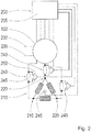
- FIG 2 shows a control device 200, in particular for operation on board a motor vehicle.
- the control unit 200 comprises the driver module 100 Figure 1 as well as a control device 205 and is set up to control a three-phase synchronous motor 210.
- the synchronous motor 210 can in particular be comprised of an actuator which influences a safety-relevant or safety-critical function on board the motor vehicle.
- steering of the motor vehicle may include an electric steering booster that is driven by the synchronous motor 210.
- the synchronous motor 210 can also be used to drive another device on board the motor vehicle be provided, for example for a window regulator, the drive of an electric hood or a seat adjustment.
- the synchronous motor 210 is configured, for example, in a star connection and comprises three phases 215 to 225, which are each set up for connection to a current source or current sink in order to control a direction of rotation, a rotational speed or a torque of the synchronous motor 210.
- phase is generally used for one of the three electrical connections of the three-phase synchronous motor 210 shown.
- the three phases 215 to 225 are connected to the control unit 200.
- the control device 205 is set up to control the driver module 100 in such a way that the individual phases 215 to 225 are connected in a defined chronological sequence to a positive potential 230 or a negative potential 235 in such a way that a predetermined rotational movement or a predetermined torque occurs on the synchronous motor 210 sets.
- control device 205 is preferably set up to determine a fault and to then switch off the driver module 100, so that the three phases 215 to 225 are neither connected to one another nor to one of the potentials 230 or 235.
- a sensor 240 can be provided on the connections between the phases 215 to 225 and the driver module 100.
- the sensor 240 can be set up to determine a voltage present at the respective phase 215 to 225 or a current flowing through the respective phase 215 to 225.
- only two sensors 240 are provided and the determination of a corresponding measured value for the remaining phases 215 to 225 takes place analytically, in particular on the basis of Kirchhoff's rules.
- the sensors 240 are set up to determine phase currents.
- a sensor 240 comprises a series resistor 245, which is also called a shunt, and of which through the respective phase 215 to 225 flowing current is flowed through.
- a voltage dropping across the series resistor 245 is determined in the present exemplary embodiment by means of a measuring amplifier 250, so that a signal proportional to the current flowing through the phases 215 to 225 is present. This signal is preferably evaluated by the control device 205.
- a malfunction in the area of the driver module 100 can, for example, result in one of the phases 215 to 225 being permanently connected to the positive potential 230 or the negative potential 235. In this case, a current flowing through the corresponding phase 215 to 225 could also be determined without appropriate activation of the driver module 100. This malfunction can also be detected by observing the phase voltages.
- a rotation sensor 245 can be provided in order to sense the rotary movement of the synchronous motor 210.
- the rotation sensor 245 can be connected to the control device 205 and the control device 205 can control the chronological sequence of the phase currents as a function of the rotation signal of the rotation sensor 245.
- a malfunction can be determined by means of the rotation sensor 245, in which the synchronous motor 210 rotates differently than would be expected from the activation of the phases 215 to 225, for example because it is mechanically blocked and does not rotate at all irrespective of its activation.
- the control device 205 can switch off the driver module 100.
- dedicated semiconductor switches 105 are preferably provided in the driver assembly 100, which are then controlled to interrupt an electrical connection between the phases 215 to 225 and further semiconductor switches 105 of the driver assembly 100, as will be described in more detail below.
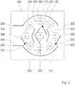
- FIG. 12 shows an exemplary line routing between the semiconductor switches 105 of the driver module 100 of FIG Figure 1 for the control unit 200 from Figure 2 .
- a preferred arrangement of the semiconductor switches 105 corresponds to the in Figure 1 illustrated embodiment used.
- a top view of the circuit board 115 without the heat sink 135 is shown. Electrical connections are shown schematically.
- the nine semiconductor switches 105 are organized in three half-bridges 305 to 315.
- Each half-bridge 305 to 315 comprises three semiconductor switches 105, one of which is used as a high-side switch 320, one as a low-side switch 325 and one as a phase separator 330.
- the phase separator 330 of a half bridge 305 to 315 is set up to establish a switchable connection to one of the phases 215 to 225.
- connection of the phase isolator 330 which is switchably connected to the respective phase 215 to 225 in this way, is connected to a connection of the high-side switch 320 in order to be switched to the positive potential 230, and to a connection of the low Side switches 325 to be switched to the negative potential 235. Simultaneous closing of the high-side switch 320 and the low-side switch 325 of the same half-bridge 305 to 315 is usually avoided by appropriate control.
- the semiconductor switches 105 preferably have the same pin assignment.
- the semiconductor switches 105 of the same type can be used for this.
- the semiconductor switches 105 of a high-side switch 320 and a low-side switch 325 can form a complementary pair, mirror-inverted pin assignments being possible.
- the semiconductor switches 105 are surface-mountable. In the representation of Figure 3 the semiconductor switches are mounted on a surface of the circuit carrier 115.
- the semiconductor switches 105 can in particular comprise field effect transistors, which are preferably used in the form of DirectFETs.
- Each of the nine semiconductor switches 105 shown can preferably be controlled separately.
- a control connection 335 is provided on each semiconductor switch 105 and can be connected to the control device 205.
- the other two connectors each semiconductor switch 105 are connected by means of connecting elements 340, which in Fig. 3 are schematically represented by wide lines, electrically connected to each other, as described above.
- the semiconductor switches 105 are preferably arranged with respect to the center 120 and the circular line 125 (both not shown) in such a way that the three phase separators 330 lie in a row or on a straight line. Two of the phase separators 330 also lie on the circular line 125 and the third phase separator 330 lies between them on the line in the region of the center 120.
- the high-side switches 320 are preferably arranged on one side of this line in FIG Figure 3 on the upper side, while the low-side switches 325 are arranged on the other side, in Figure 3 on the bottom. Both the high-side switches 320 and the low-side switches 325 lie on the circular line 125.
- Connections between the semiconductor switches 105, between the semiconductor switches 105 and the potentials 230 and 235, and between the semiconductor switches 105 and connections for the phases 215 to 225 can, as in FIG Figure 3 is shown, be easy to cross and also be kept short. Connections between the control ports 335 and the controller 205 can be easily unbundled in a known manner. In a preferred embodiment, all electrical connections that lead to control connections 335 are routed in a different plane than the connection elements 340 that carry the currents that flow through the phases 215 to 225 of the synchronous motor 210. For this purpose, a circuit carrier 115 with several levels can be used, on which the connecting elements 340 can be guided. In the illustrated embodiment, the current-carrying connection elements 340 are guided on the top side of the circuit carrier 115, while connection elements for contacting the control connections 335 can be laid on the underside of the circuit carrier 115 by means of plated-through holes.
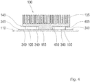
- Figure 4 10 shows a side view of an embodiment of driver assembly 100 of FIG Figure 1 .
- the base area 140 of the heat sink 135 bears against the upper surfaces of the semiconductor switches 105.
- the thermal coupling of the heat sink 135 to the semiconductor switches 105 is preferably carried out by means of an interposed one Heat-conducting agent 405.
- the heat-conducting agent 405 preferably has a low thermal resistance and is preferably set up to bridge gaps of different widths between the upper surfaces of the semiconductor switches 105 and the base area 140 of the heat sink 135. Vertical assembly tolerances of the semiconductor switches 105 can thereby be compensated for.
- the heat conducting means 405 is electrically insulating.
- the heat conducting means 405 can comprise, for example, a heat conducting pad, a heat conducting paste or a mica disk.
- the heat sink 135 can comprise a projection 410, which is configured to bear against a connecting element 340.
- a heat-conducting element 405 can also be provided between the projection 410 and the connecting element 340.
- the connecting element 340 can be cooled in an improved manner by means of the projection 410.
- a heat input along the connecting element 340 into one of the semiconductor switches 105 can thereby be reduced.
- a connecting element 340 which electrically connects two semiconductor switches 105 to one another, can be cooled by means of the projection 410. As a result, thermal insulation of the two semiconductor switches 105 can be improved.
- a size, position and shape of the projection 410 can be selected in such a way that a heat flow between the semiconductor switches 105 is influenced in such a way that the semiconductor switches 105 are heated essentially equally during operation.
- a plurality of protrusions 410 can be provided between pairs of semiconductor switches 106, wherein the protrusions 410 can also be shaped differently. The sizes and shapes of the protrusions 410 can be selected such that uniform heating of the semiconductor switches 105 is ensured during operation.
- protrusions 410 only extend toward those in FIGS Figure 3 extend connecting elements 340 shown with broad lines, which are traversed by currents which flow through the phases 215 to 225 of the synchronous motor 210.
Landscapes
- Engineering & Computer Science (AREA)
- Power Engineering (AREA)
- Microelectronics & Electronic Packaging (AREA)
- Physics & Mathematics (AREA)
- Thermal Sciences (AREA)
- Control Of Ac Motors In General (AREA)
- Inverter Devices (AREA)
- Control Of Direct Current Motors (AREA)
- Electronic Switches (AREA)
- Power Steering Mechanism (AREA)
Description
- Die Erfindung betrifft eine Treiberbaugruppe. Insbesondere betrifft die Erfindung die Anordnung von Elementen der Treiberbaugruppe.
- Ein Steuergerät, beispielsweise an Bord eines Kraftfahrzeugs, ist dazu eingerichtet, einen Strom oder eine Spannung bereitzustellen, um einen angeschlossenen Verbraucher zu steuern. Beispielsweise kann eine Dreiphasen-Wechselspannung bereitgestellt werden, um die Drehrichtung, das Drehmoment oder die Drehgeschwindigkeit eines angeschlossenen Synchronmotors zu steuern.
- Eine Treiberbaugruppe umfasst mehrere Halbleiterschalter, um den benötigten Strom bzw. die benötigte Spannung für den Synchronmotor bereitzustellen. Die Halbleiterschalter arbeiten üblicherweise nicht verlustfrei, sodass Wärme von ihnen abgeführt werden muss. Um Zuleitungen zu den Halbleiterschaltern möglichst kurz und direkt zu führen und mittels eines gemeinsamen Kühlkörpers kühlen zu können, sind die Halbleiterschalter üblicherweise matrixförmig oder zufällig angeordnet. Im Betrieb erwärmen sich die Halbleiterschalter in Abhängigkeit ihrer Anordnung unterschiedlich stark gegenseitig, sodass sie unterschiedliche Temperaturen annehmen. Durch die unterschiedlichen Temperaturen können die Halbleiterschalter elektrisch unterschiedlich stark belastbar sein, sodass die elektrische Gesamtbelastbarkeit der Treiberbaugruppe reduziert sein kann. Die Halbleiterschalter können auch unterschiedlich stark bzw. schnell altern, sodass ihre Ausfallwahrscheinlichkeiten unterschiedlich sind. Die Ausfallwahrscheinlichkeit der gesamten Treiberbaugruppe kann dadurch erhöht sein. Außerdem können Zuleitungen zu den Halbleiterschaltern unterschiedlich lang sein, wodurch eine elektromagnetische Verträglichkeit (EMV), eine Impedanz oder ein Spannungsabfall im Bereich der Zuleitungen negativ beeinflusst sein kann.
- Die deutsche Offenlegungsschrift
DE10252315A1 offenbart eine Treiberbaugruppe, die zur Steuerung eines Elektromotors dient, und ein Stanzgitter aufweist, das dazu dient die Verbindungsleitungen, Halbleiterschalter und Phasenwicklungen des Elekt ronmotors elektrisch zu verbinden. Die Ausführung des Stanzgitters ist so, dass die Halbleiterschalter in zwei konzentrischen Kreisen angeordnet sind. - Die
DE10306227 zeigt einen Umrichter mit neun kreisförmig angeordneten Halbleiterschaltern. - Es ist Aufgabe der vorliegenden Erfindung, eine verbesserte Treiberbaugruppe anzugeben. Die Erfindung löst diese Aufgabe mittels einer Treiberbaugruppe mit den Merkmalen des unabhängigen Anspruchs. Unteransprüche geben bevorzugte Ausführungsformen wieder.
- Eine erfindungsgemäße Treiberbaugruppe umfasst eine vorbestimmte Anzahl Halbleiterschalter, wobei einer der Halbleiterschalter innerhalb einer Kreislinie und die restlichen Halbleiterschalter auf der Kreislinie angeordnet sind. Dadurch können sich die Halbleiterschalter im Betrieb im Wesentlichen gleichmäßig erwärmen. Vorzugsweise sind der eine Halbleiterschalter angrenzend zu einem Mittelpunkt eines Kreises und die restlichen Halbleiterschalter auf einer Kreislinie um den Mittelpunkt angeordnet. Dadurch kann die im Wesentlichen gleichmäßige Erwärmung der Halbleiterschalter weiter optimiert werden. Thermische Belastungen der Halbleiterschalter können im Wesentlichen gleich sein, sodass auch elektrische Belastbarkeiten der Halbleiterschalter gleich sein können. Eine elektrische Belastbarkeit der gesamten Treiberbaugruppe kann dadurch insgesamt erhöht sein. Alternativ dazu können die Halbleiterschalter bei gleicher Belastbarkeit schwächer dimensioniert werden. Durch die gleichen thermischen Belastungen können die Halbleiterschalter auch gleich stark oder gleich schnell altern, wodurch die elektrischen Belastbarkeiten über die Lebensdauer der Halbleiterschalter vergleichbar bleiben können. Die elektrische Belastbarkeit der Treiberbaugruppe kann dadurch auf lange Sicht stabil sein. Die langfristige Zuverlässigkeit der Treiberbaugruppe kann erhöht sein. Dies ist insbesondere bei der Ansteuerung eines sicherheitskritischen Elements, beispielsweise einer elektrischen Lenkhilfe an Bord eines Kraftfahrzeugs, von Vorteil.
- Bevorzugterweise sind die auf der Kreislinie liegenden Halbleiterschalter gleichmäßig verteilt. Dazu können auf der Kreislinie benachbarte Halbleiterschalter jeweils den gleichen Winkel bezüglich des Mittelpunkts einschließen. Die Anordnung der Halbleiterschalter kann toleranzbehaftet sein, indem an der Oberfläche jedes Halbleiterschalters ein beliebiger Punkt gewählt wird, dessen Position auf der Kreislinie oder bezüglich der anderen Halbleiterschalter wie beschrieben eingehalten ist. In einer anderen Ausführungsform haben die Halbleiterschalter vergleichbare Bauformen und die Punkte an den Oberflächen der Halbleiterschalter werden vergleichbar gewählt. Beispielsweise kann der Punkt jeweils am geometrischen Mittelpunkt oder im Bereich der stärksten Erwärmung während des Betriebs gewählt sein.
- Insbesondere dann, wenn der gewählte Punkt im Bereich der stärksten Erwärmung gewählt ist, kann eine rotatorische Ausrichtung der einzelnen Halbleiterschalter bezüglich der Wärmeverteilung beliebig gewählt sein. In einer anderen Ausführungsform können die einzelnen Halbleiterschalter auch bezüglich kleinster Abstände ihrer Umrisse aneinander ausgerichtet werden. Dies kann insbesondere dann vorteilhaft sein, wenn die Oberflächen der Halbleiterschalter relativ groß sind und sich eine Oberfläche im Betrieb relativ gleichmäßig erwärmt.
- In einer weiteren Ausführungsform können Abstände der auf der Kreislinie liegenden Halbleiterschalter zum mittleren Halbleiterschalter gleich groß sein. Die Erwärmung des mittleren Halbleiterschalters, der potentiell am stärksten einem Wärmeeintrag durch die restlichen Halbleiterschalter ausgesetzt ist, kann dadurch verbessert kontrolliert werden. Gleichmäßige Temperaturen der Halbleiterschalter können so leichter erreicht werden.
- In einer besonders bevorzugten Ausführungsform ist die Treiberbaugruppe zur Ansteuerung eines Dreiphasen-Synchronmotors eingerichtet. Dazu umfasst die Treiberbaugruppe drei Halbbrücken mit insgesamt neun Halbleiterschaltern. Jede Halbbrücke umfasst drei Halbleiterschalter, die als High-Side-Switch, Low-Side-Switch und Phasentrenner miteinander verschaltet sind. Dabei ist der Phasentrenner zur Verbindung eines Mittenabgriffs zwischen dem High-Side-Switch und dem Low-Side-Switch mit einem Phasenanschluss des Synchronmotors vorgesehen.
- Dadurch kann eine kompakte und thermisch stabile Treiberbaugruppe zur Ansteuerung des Synchronmotors angegeben werden, die durch die zusätzlichen Phasentrenner eine verbesserte Steuerbarkeit aufweist. Insbesondere ist es möglich, den Synchronmotor mittels der Phasentrenner abzuschalten, wenn beispielsweise ein fehlerhafter Zustand erfasst wurde. Ein Synchronmotor in einem sicherheitsrelevanten oder sicherheitskritischen System kann dadurch verbessert in einen sicheren Zustand gebracht werden, in dem der Synchronmotor weder kurzgeschlossen noch stromdurchflossen ist. Beispielsweise kann der Synchronmotor zur Verstärkung oder Abschwächung einer fahrerbewirkten Lenkkraft in einem Kraftfahrzeug dienen. Wird der Synchronmotor mittels der Phasentrenner abgeschaltet, so kann die Lenkkraft weder verstärkt noch verringert werden. Ein vorbestimmtes Lenkverhalten des Kraftfahrzeugs kann dadurch auch im Fehlerfall sichergestellt sein.
- Bevorzugterweise sind die drei Halbleiterschalter der Phasentrenner in einer Reihe angeordnet und auf der einen Seite der Reihe sind die drei High-Side-Switches und auf der anderen die drei Low-Side-Switches angeordnet. Dabei ist der in der Mitte liegende Halbleiterschalter zwangsläufig ein Phasentrenner. Die Symmetrie der Wärmeverteilung in der Treiberbaugruppe kann dadurch verbessert sein. Außerdem können elektrische Verbindungen zwischen den einzelnen Halbleiterschaltern leichter kreuzungsfrei geführt werden. Durch die verbesserte Führung der Verbindungen können eine elektromagnetische Verträglichkeit, eine Impedanz und ein Leitungswiderstand der Verbindungen verbessert bzw. aneinander angeglichen werden. Die Treiberbaugruppe kann dadurch präziser steuerbar oder weniger störungsanfällig sein.
- Die Halbleiterschalter können oberflächenmontierbare Bauelemente mit gleichen Pinbelegungen sein. Die Leitungsführung zwischen den Halbleiterschaltern, insbesondere bei der zuletzt beschriebenen Anordnung, kann dadurch weiter erleichtert sein. Die elektrischen Verbindungen, die den durch die Phasen des Synchronmotors fließenden Strom führen, können erleichtert kreuzungsfrei in einer Ebene geführt werden. Ein passender Schaltungsträger für die Halbleiterschalter, beispielsweise eine Platine mit aufgebrachten Leiterbahnen, kann dadurch leichter planbar und herstellbar sein. Die Erwärmung des Schaltungsträgers kann zudem verbessert kontrollierbar sein.
- Bevorzugterweise ist ein Kühlkörper zur Anlage an den Halbleiterschaltern vorgesehen. Der Kühlkörper kann insbesondere eine kreisförmige Grundfläche aufweisen, die in Anlage mit den einzelnen Halbleiterschaltern steht. Dadurch kann eine zylinderförmige Anordnung von gleichmäßig gekühlten Halbleiterschaltern entstehen, die von der Treiberbaugruppe umfasst ist. Der Kühlkörper kann so an den Halbleiterschaltern angebracht sein, dass die dadurch entstandene Einheit separat handhabbar ist, wodurch beispielsweise ein Montageprozess der Treiberbaugruppe in einem Steuergerät zur Ansteuerung des Synchronmotors erleichtert sein kann. Außerdem kann die runde Form des Kühlkörpers bzw. der Einheit mit einer zylindrischen Form des Synchronmotors korrespondieren, sodass verbessert eine platzsparende Anbringung der Einheit am Synchronmotor möglich ist.
- In einer bevorzugten Ausführungsform umfasst der Kühlkörper einen Vorsprung zur Anlage an einem an der Oberfläche liegenden elektrischen Verbindungselement zwischen zwei Halbleiterschaltern. Im Fall des oben beschriebenen Schaltungsträgers kann beispielsweise eine Leiterbahn durch den Vorsprung kontaktiert sein. Der Vorsprung kann dazu beitragen, dass ein Wärmeeintrag von einem Halbleiterschalter zu einem anderen mittels des elektrischen Verbindungselements verringert oder kompensiert wird. Außerdem kann der Vorsprung zur verbesserten mechanischen Befestigung des Kühlkörpers an dem Schaltungsträger dienen.
- Es ist besonders bevorzugt, dass mehrere Vorsprünge derart zwischen den Halbleiterschaltern vorgesehen sind, dass sich die Halbleiterschalter im Betrieb auf gleiche Temperaturen erwärmen. Die Dimensionierung und Positionierung der Vorsprünge kann beispielsweise mittels Berechnungen, einer Simulation oder Versuch und Irrtum bestimmt werden. Je größer das Volumen eines Vorsprungs ist, desto stärker ist seine Wärmeableitung, sodass zwei Halbleiterschalter, die mit einem an dem Vorsprung anliegenden Verbindungselement verbunden sind, verbessert thermisch voneinander isoliert werden können.
- In einer weiteren Ausführungsform ist ferner eine Steuereinrichtung zur Ansteuerung der Halbbrücken vorgesehen. Die Steuereinrichtung ist dazu eingerichtet, Phasenspannungen oder Phasenströme des Synchronmotors zu überwachen und den Synchronmotor mittels der Phasentrenner auszuschalten, falls die bestimmten Phasenspannungen oder Phasenströme auf einen Defekt eines der High-Side-Switches oder eines der Low-Side-Switches hinweisen. Eine Baugruppe, die die Treiberbaugruppe, die Steuereinrichtung und den Synchronmotor umfasst, kann dadurch auch im Fehlerfall in einen sicheren Zustand gebracht werden. Dies kann insbesondere bei dem oben beschriebenen sicherheitsrelevanten System an Bord eines Kraftfahrzeugs, beispielsweise an der Lenkhilfe, vorteilhaft sein.
- Die Erfindung wird nun mit Bezug auf die beigefügten Figuren genauer beschrieben, in denen:
- Figur 1
- eine Anordnung von Halbleiterschaltern einer Treiberbaugruppe;
- Figur 2
- ein Schaltbild einer Baugruppe mit der Treiberbaugruppe von
Figur 1 ; - Figur 3
- eine Leitungsführung zwischen den Halbleiterschaltern der Treiberbaugruppe von
Figur 1 und - Figur 4
- eine Seitenansicht einer Ausführungsform der Treiberbaugruppe von Figur 1
-
Figur 1 zeigt eine schematische Draufsicht auf eine Treiberbaugruppe 100 mit mehreren Halbleiterschaltern 105. Die Halbleiterschalter 105 sind bevorzugterweise oberflächenmontierbare Bauelemente, die in einer Ebene 110 angeordnet sind, die insbesondere durch die Oberfläche eines Schaltungsträgers 115, etwa einer Platine, gebildet ist. Die Halbleiterschalter können beispielsweise Bipolartransistoren, Feldeffekttransistoren, MOSFETs, Thyristoren, Schaltdioden oder IGBTs umfassen. In beispielhafter Weise sind die neun Halbleiterschalter 105 vorgesehen, deren elektrische Konfiguration unten noch genauer beschrieben wird. Einer der Halbleiterschalter 105 ist im Bereich eines Mittelpunkts 120 einer Kreislinie 125 angeordnet, während die restlichen Halbleiterschalter 105 auf der Kreislinie 125 liegen. - Zur Bestimmung der Position eines Halbleiterschalters 105 kann ein Punkt 130 innerhalb seines Umrisses gewählt sein, dessen exakte Position auf der Kreislinie 125 oder auf dem Mittelpunkt 120 bestimmt werden kann. Bevorzugterweise weisen die Halbleiterschalter 105 gleiche Umrisse auf und die Punkte 130 sind an korrespondierenden Stellen gewählt. Die Stellen können beispielsweise aufgrund von geometrischen oder thermischen Überlegungen, etwa an einem geometrischen Mittelpunkt oder an einem Punkt der stärksten Erwärmung, gewählt sein. In der Darstellung von
Figur 1 sind die Punkte 130 an den Halbleiterschaltern korrespondierend aber außermittig gewählt. Dabei fällt der Punkt 130 des mittleren Halbleiterschalters 105 auf den Mittelpunkt 120. Die Punkte 130 der restlichen acht Halbleiterschalter 105 sind auf der Kreislinie 125 gleichmäßig verteilt, sodass benachbarte Punkte 130 bezüglich des Mittelpunkts 120 jeweils einen Winkel von 360° : 8 = 45° einschließen. - Bevorzugterweise sind die Halbleiterschalter 105 thermisch mit einem Kühlkörper 135 gekoppelt. Der Kühlkörper 135 weist bevorzugterweise eine runde Grundfläche 140 zur Anlage an Oberflächen der Halbleiterschalter 105 auf. In einer anderen Ausführungsform kann die Grundfläche 140 auch gleichmäßig polygonal mit so vielen Ecken sein, wie Halbleiterschalter 105 auf der Kreislinie 125 angeordnet sind. Dadurch kann die Treiberbaugruppe 100 eine im Wesentlichen zylindrische Form erhalten, die mit einer zylindrischen Form eines Endabschnitts eines Synchronmotors korrespondieren kann, der durch die Treiberbaugruppe 100 steuerbar ist. Die Treiberbaugruppe 100 kann im Bereich des Endabschnitts vorteilhaft platzsparend am Synchronmotor angeordnet werden. Insbesondere kann die Treiberbaugruppe 100 in axialer Verlängerung des Endabschnitts angeordnet sein, wodurch die Treiberbaugruppe 100 mit dem Synchronmotor eine separat handhabbare Einheit bilden kann. Der Synchronmotor und die Treiberbaugruppe 100 können in einem gemeinsamen Gehäuse angeordnet sein.
- Der Kühlkörper 135 kann thermisch mittels eines Wärmeleitpads, einer Wärmeleitpaste oder einer Glimmerscheibe, verbessert angebunden sein. Dadurch kann eine elektrische Isolation der Halbleiterschalter 105 vom Kühlkörper 135 bewirkt sein, die insbesondere dann vorteilhaft ist, wenn ein elektrischer Anschluss eines Halbleiterschalters 105 an dessen Oberfläche liegt. Dies ist beispielsweise der Fall bei sogenannten DirectFETs, die als Halbleiterschalter 105 in der Treiberbaugruppe 100 bevorzugt verwendet werden.
-
Figur 2 zeigt ein Steuergerät 200, insbesondere zum Betrieb an Bord eines Kraftfahrzeugs. Das Steuergerät 200 umfasst die Treiberbaugruppe 100 ausFigur 1 sowie eine Steuereinrichtung 205 und ist dazu eingerichtet, einen Dreiphasen-Synchronmotor 210 anzusteuern. Der Synchronmotor 210 kann insbesondere von einem Aktuator umfasst sein, der eine sicherheitsrelevante oder sicherheitskritische Funktion an Bord des Kraftfahrzeugs beeinflusst. Beispielsweise kann eine Lenkung des Kraftfahrzeugs einen elektrischen Lenkkraftverstärker umfassen, der durch den Synchronmotor 210 angetrieben wird. In anderen Ausführungsformen kann der Synchronmotor 210 auch für den Antrieb einer anderen Einrichtung an Bord des Kraftfahrzeugs vorgesehen sein, beispielsweise für einen Fensterheber, den Antrieb eines elektrischen Verdecks oder einer Sitzverstellung. - Der Synchronmotor 210 ist beispielhaft in Sternschaltung konfiguriert und umfasst drei Phasen 215 bis 225, die jeweils zur Verbindung mit einer Stromquelle oder Stromsenke eingerichtet sind, um eine Drehrichtung, eine Drehgeschwindigkeit oder ein Drehmoment des Synchronmotors 210 zu steuern. Im Folgenden wird der Begriff Phase allgemein für einen der drei elektrischen Anschlüsse des dargestellten Dreiphasen-Synchronmotors 210 verwendet.
- Die drei Phasen 215 bis 225 sind mit dem Steuergerät 200 verbunden. Die Steuereinrichtung 205 ist dazu eingerichtet, die Treiberbaugruppe 100 derart anzusteuern, dass die einzelnen Phasen 215 bis 225 in definierter zeitlicher Abfolge derart mit einem positiven Potential 230 oder einem negativen Potential 235 verbunden werden, dass sich eine vorbestimmte Drehbewegung oder ein vorbestimmtes Drehmoment am Synchronmotor 210 einstellt.
- Zusätzlich ist die Steuereinrichtung 205 bevorzugterweise dazu eingerichtet, einen Fehlerfall zu bestimmen und die Treiberbaugruppe 100 daraufhin abzustellen, sodass die drei Phasen 215 bis 225 weder untereinander noch mit einem der Potentiale 230 oder 235 verbunden sind.
- Dazu kann an den Verbindungen zwischen den Phasen 215 bis 225 und der Treiberbaugruppe 100 jeweils ein Sensor 240 vorgesehen sein. Der Sensor 240 kann zur Bestimmung einer an der jeweiligen Phase 215 bis 225 anliegenden Spannung oder eines durch die jeweilige Phase 215 bis 225 fließenden Stroms eingerichtet sein. In einer weiteren Ausführungsform sind nur zwei Sensoren 240 vorgesehen und die Bestimmung eines korrespondierenden Messwerts für die verbleibende Phase 215 bis 225 erfolgt analytisch, insbesondere auf der Basis der Kirchhoff'schen Regeln.
- In der vorliegenden Ausführungsform sind die Sensoren 240 zur Bestimmung von Phasenströmen eingerichtet. Ein Sensor 240 umfasst hierfür einen Längswiderstand 245, der auch Shunt genannt wird, und der von dem durch die jeweilige Phase 215 bis 225 fließenden Strom durchflossen wird. Eine über dem Längswiderstand 245 abfallende Spannung wird in der vorliegenden, beispielhaften Ausführungsform mittels eines Messverstärkers 250 bestimmt, sodass ein zum durch die Phase 215 bis 225 fließenden Strom proportionales Signal vorliegt. Dieses Signal wird bevorzugterweise von der Steuereinrichtung 205 ausgewertet.
- Eine Fehlfunktion im Bereich der Treiberbaugruppe 100 kann beispielsweise dazu führen, dass eine der Phasen 215 bis 225 permanent mit dem positiven Potential 230 oder dem negativen Potential 235 verbunden ist. In diesem Fall könnte ein durch die entsprechende Phase 215 bis 225 fließender Strom auch ohne entsprechende Ansteuerung der Treiberbaugruppe 100 festgestellt werden. Diese Fehlfunktion kann auch durch Beobachten der Phasenspannungen detektiert werden.
- In einer weiteren Ausführungsform kann ein Drehsensor 245 vorgesehen sein um die Drehbewegung des Synchronmotors 210 abzutasten. Der Drehsensor 245 kann mit der Steuereinrichtung 205 verbunden sein und die Steuereinrichtung 205 kann die zeitliche Abfolge der Phasenströme in Abhängigkeit des Drehsignals des Drehsensors 245 steuern. Außerdem kann mittels des Drehsensors 245 eine Fehlfunktion bestimmt werden, bei der sich der Synchronmotor 210 anders dreht als durch die Ansteuerung der Phasen 215 bis 225 zu erwarten wäre, beispielsweise weil er mechanisch blockiert ist und sich unabhängig von seiner Ansteuerung überhaupt nicht dreht.
- Wird also eine Fehlfunktion festgestellt, so kann die Steuereinrichtung 205 die Treiberbaugruppe 100 abschalten. Bevorzugterweise sind hierfür in der Treiberbaugruppe 100 dedizierte Halbleiterschalter 105 vorgesehen, die dann angesteuert werden, eine elektrische Verbindung zwischen den Phasen 215 bis 225 und weiteren Halbleiterschaltern 105 der Treiberbaugruppe 100 zu unterbrechen, wie im Folgenden genauer beschrieben wird.
-
Figur 3 zeigt eine beispielhafte Leitungsführung zwischen den Halbleiterschaltern 105 der Treiberbaugruppe 100 vonFigur 1 für das Steuergerät 200 vonFigur 2 . Dabei wird eine bevorzugte Anordnung der Halbleiterschalter 105 entsprechend der inFigur 1 dargestellten Ausführungsform verwendet. Gezeigt ist eine Draufsicht auf die Platine 115 ohne den Kühlkörper 135. Elektrische Verbindungen sind schematisch dargestellt. - In der dargestellten, bevorzugten Ausführungsform sind die neun Halbleiterschalter 105 in drei Halbbrücken 305 bis 315 organisiert. Jede Halbbrücke 305 bis 315 umfasst drei Halbleiterschalter 105, von denen einer als High-Side-Switch 320, einer als Low-Side-Switch 325 und einer als Phasentrenner 330 verwendet wird. Der Phasentrenner 330 einer Halbbrücke 305 bis 315 ist dazu eingerichtet, eine schaltbare Verbindung zu einer der Phasen 215 bis 225 herzustellen. Der Anschluss des Phasentrenners 330, der auf diese Weise schaltbar mit der jeweiligen Phase 215 bis 225 verbunden ist, ist mit einem Anschluss des High-Side-Switches 320 verbunden, um an das positive Potential 230 geschaltet zu werden, und einem Anschluss des Low-Side-Switches 325, um an das negative Potential 235 geschaltet zu werden. Dabei wird ein gleichzeitiges Schließen des High-Side-Switches 320 und des Low-Side-Switches 325 derselben Halbbrücke 305 bis 315 üblicherweise durch eine entsprechende Ansteuerung vermieden.
- Die Halbleiterschalter 105 weisen bevorzugterweise die gleiche Pinbelegung auf. Dazu können die Halbleiterschalter 105 des gleichen Typs verwendet werden. In einer anderen Ausführungsform können die Halbleiterschalter 105 eines High-Side-Switches 320 und eines Low-Side-Switches 325 ein Komplementärpaar bilden, wobei spiegelverkehrte Pinbelegungen möglich sind.
- Außerdem ist bevorzugt, dass die Halbleiterschalter 105 oberflächenmontierbar sind. In der Darstellung von
Figur 3 sind die Halbleiterschalter auf einer Oberfläche des Schaltungsträgers 115 angebracht. Die Halbleiterschalter 105 können insbesondere Feldeffekttransistoren umfassen, die bevorzugterweise in der Bauform von DirectFETs verwendet werden. - Jeder der neun dargestellten Halbleiterschalter 105 ist bevorzugterweise separat ansteuerbar. An jedem Halbleiterschalter 105 ist ein Steueranschluss 335 vorgesehen, der mit der Steuereinrichtung 205 verbunden werden kann. Die anderen beiden Anschlüsse jedes Halbleiterschalters 105 werden mittels Verbindungselementen 340, die in
Fig. 3 schematisch durch breite Linien dargestellt sind, elektrisch miteinander verbunden, wie oben beschrieben ist. Bevorzugterweise sind die Halbleiterschalter 105 derart bezüglich des Mittelpunkts 120 und der Kreislinie 125 (beide nicht dargestellt) angeordnet, dass die drei Phasentrenner 330 in einer Reihe bzw. auf einer geraden Linie liegen. Zwei der Phasentrenner 330 liegen dabei auch auf der Kreislinie 125 und der dritte Phasentrenner 330 liegt zwischen ihnen auf der Linie im Bereich des Mittelpunkts 120. Bevorzugterweise sind die High-Side-Switches 320 auf der einen Seite dieser Linie angeordnet, inFigur 3 auf der oberen Seite, während die Low-Side-Switches 325 auf der anderen Seite angeordnet sind, inFigur 3 auf der unteren Seite. Sowohl die High-Side-Switches 320 als auch die Low-Side-Switches 325 liegen dabei auf der Kreislinie 125. - Verbindungen zwischen den Halbleiterschaltern 105, zwischen den Halbleiterschaltern 105 und den Potentialen 230 und 235, und zwischen den Halbleiterschaltern 105 und Anschlüssen für die Phasen 215 bis 225 können, wie in
Figur 3 gezeigt ist, leicht kreuzungsfrei und auch kurz gehalten sein. Verbindungen zwischen den Steueranschlüssen 335 und der Steuereinrichtung 205 können auf eine bekannte Weise leicht entflochten werden. In einer bevorzugten Ausführungsform werden alle elektrischen Verbindungen, die zu Steueranschlüssen 335 führen, in einer anderen Ebene geführt als die Verbindungselemente 340, die die Ströme führen, die durch die Phasen 215 bis 225 des Synchronmotors 210 fließen. Hierzu kann ein Schaltungsträger 115 mit mehreren Ebenen verwendet werden, auf denen die Verbindungselemente 340 geführt werden können. In der dargestellten Ausführungsform werden die stromführenden Verbindungselemente 340 auf der Oberseite des Schaltungsträgers 115 geführt, während Verbindungselemente zur Kontaktierung der Steueranschlüsse 335 mittels Durchkontaktierungen auf die Unterseite des Schaltungsträgers 115 verlegt werden können. -
Figur 4 zeigt eine Seitenansicht einer Ausführungsform der Treiberbaugruppe 100 vonFigur 1 . Die Grundfläche 140 des Kühlkörpers 135 liegt an oberen Oberflächen der Halbleiterschalter 105 an. Bevorzugterweise erfolgt die thermische Kopplung des Kühlkörpers 135 mit den Halbleiterschaltern 105 mittels eines dazwischen eingefügten Wärmeleitmittels 405. Das Wärmeleitmittel 405 hat bevorzugterweise einen geringen Wärmewiderstand und ist bevorzugterweise dazu eingerichtet, unterschiedlich breite Spalte zwischen den oberen Oberflächen der Halbleiterschalter 105 und der Grundfläche 140 des Kühlkörpers 135 zu überbrücken. Dadurch können vertikale Montagetoleranzen der Halbleiterschalter 105 ausgeglichen werden. Ferner ist bevorzugt, dass das Wärmeleitmittel 405 elektrisch isolierend ist. Das Wärmeleitmittel 405 kann beispielsweise ein Wärmeleitpad, eine Wärmeleitpaste oder eine Glimmerscheibe umfassen. - Der Kühlkörper 135 kann einen Vorsprung 410 umfassen, der dazu eingerichtet ist, an einem Verbindungselement 340 anzuliegen. Zwischen dem Vorsprung 410 und dem Verbindungselement 340 kann ebenfalls ein Wärmeleitelement 405 vorgesehen sein. Vermittels des Vorsprungs 410 kann das Verbindungselement 340 verbessert gekühlt werden. Ein Wärmeeintrag entlang des Verbindungselements 340 in einen der Halbleiterschalter 105 kann dadurch reduziert werden. Insbesondere kann ein Verbindungselement 340, das zwei Halbleiterschalter 105 elektrisch miteinander verbindet, mittels des Vorsprungs 410 gekühlt werden. Dadurch kann eine thermische Isolation der beiden Halbleiterschalter 105 verbessert sein.
- Eine Größe, Position und Form des Vorsprungs 410 kann so gewählt werden, dass ein Wärmefluss zwischen den Halbleiterschaltern 105 derart beeinflusst wird, dass die Halbleiterschalter 105 im Betrieb im Wesentlichen gleich erwärmt werden. Mehrere Vorsprünge 410 zwischen Paaren von Halbleiterschaltern 106 können vorgesehen sein, wobei die Vorsprünge 410 auch unterschiedlich geformt sein können. Größen und Formen der Vorsprünge 410 können so gewählt sein, dass eine gleichmäßige Erwärmung der Halbleiterschalter 105 im Betrieb gewährleistet ist.
- Allgemein ist bevorzugt, dass sich Vorsprünge 410 nur zu den in
Figur 3 mit breiten Linien dargestellten Verbindungselementen 340 erstrecken, die von Strömen durchflossen sind, die durch die Phasen 215 bis 225 des Synchronmotors 210 fließen. -
- 100
- Treiberbaugruppe
- 105
- Halbleiterschalter
- 110
- Ebene
- 115
- Schaltungsträger (Platine)
- 120
- Mittelpunkt
- 125
- Kreislinie
- 130
- Punkt
- 135
- Kühlkörper
- 140
- Grundfläche
- 200
- Steuergerät
- 205
- Steuereinrichtung
- 210
- Dreiphasen-Synchronmotor
- 215
- erste Phase
- 220
- zweite Phase
- 225
- dritte Phase
- 230
- positives Potential
- 235
- negatives Potential
- 240
- Sensor
- 245
- Längswiderstand (Shunt)
- 250
- Messverstärker
- 305
- erste Halbbrücke
- 310
- zweite Halbbrücke
- 315
- dritte Halbbrücke
- 320
- High-Side-Switch
- 325
- Low-Side-Switch
- 330
- Phasentrenner
- 335
- Steueranschluss
- 340
- Verbindungselement
- 405
- Wärmeleitmittel
- 410
- Vorsprung
Claims (8)
- Treiberbaugruppe (100), wobei die Treiberbaugruppe (100) folgendes umfasst:
eine vorbestimmte Anzahl Halbleiterschalter (105), wobei einer der Halbleiterschalter (105) innerhalb einer Kreislinie (125) und die restlichen Halbleiterschalter (105) auf der Kreislinie (125) angeordnet sind, dadurch gekennzeichnet, dass Abstände der auf der Kreislinie (125) liegenden Halbleiterschalter (105) zum mittleren Halbleiterschalter (105) gleich groß sind, und dass insgesamt neun Halbleiterschalter (105) vorgesehen sind, die Treiberbaugruppe (100) drei Halbbrücken (305, 310, 315) zur Ansteuerung eines Dreiphasen-Synchronmotors (210) umfasst und- jede Halbbrücke (305, 310, 315) drei Halbleiterschalter (105) umfasst, die als High-Side-Switch (320), Low-Side-Switch (325) und Phasentrenner (330) miteinander verschaltet sind;- wobei der Phasentrenner (330) zur Verbindung eines Mittenabgriffs zwischen dem High-Side-Switch (320) und dem Low-Side-Switch (325) mit einem Phasenanschluss (215, 220, 225) des Synchronmotors (210) vorgesehen ist. - Treiberbaugruppe (100) nach Anspruch 1, dadurch gekennzeichnet, dass die auf der Kreislinie (125) liegenden Halbleiterschalter (105) gleichmäßig verteilt sind.
- Treiberbaugruppe (100) nach Anspruch 3, dadurch gekennzeichnet, dass die drei Halbleiterschalter (105) der Phasentrenner (330) in einer Reihe angeordnet sind und auf der einen Seite der Reihe die drei High-Side-Switches (320) und auf der anderen die drei Low-Side-Switches (325) angeordnet sind.
- Treiberbaugruppe (100) nach einem der vorangehenden Ansprüche, dadurch gekennzeichnet, dass die Halbleiterschalter (105) oberflächenmontierbare Bauelemente mit gleichen Pinbelegungen sind.
- Treiberbaugruppe (100) nach einem der vorangehenden Ansprüche, ferner umfassend einen Kühlkörper (135) zur Anlage an den Halbleiterschaltern (105).
- Treiberbaugruppe (100) nach Ansprüchen 4 und 5, dadurch gekennzeichnet, dass der Kühlkörper (135) einen Vorsprung (410) zur Anlage an einem an der Oberfläche liegenden elektrischen Verbindungselement (340) zwischen zwei Halbleiterschaltern (105) umfasst.
- Treiberbaugruppe (100) nach Anspruch 6, dadurch gekennzeichnet, dass mehrere Vorsprünge (410) derart zwischen den Halbleiterschaltern (105) vorgesehen sind, dass sich die Halbleiterschalter (105) im Betrieb auf gleiche Temperaturen erwärmen.
- Treiberbaugruppe (100) nach einem der vorangehenden Ansprüche, dadurch gekennzeichnet, dass ferner eine Steuereinrichtung (205) zur Ansteuerung der Halbbrücken (305, 310, 315) vorgesehen ist, wobei die Steuereinrichtung (205) ferner dazu eingerichtet ist, Phasenspannungen oder Phasenströme des Synchronmotors (210) zu überwachen und den Synchronmotor (210) mittels der Phasentrenner (330) auszuschalten, falls die bestimmten Phasenspannungen oder Phasenströme auf einen Defekt eines der High-Side-Switches (320) oder eines der Low-Side-Switches (325) hinweisen.
Applications Claiming Priority (2)
| Application Number | Priority Date | Filing Date | Title |
|---|---|---|---|
| DE102014205957.7A DE102014205957A1 (de) | 2014-03-31 | 2014-03-31 | Treiberbaugruppe |
| PCT/EP2015/053466 WO2015149986A1 (de) | 2014-03-31 | 2015-02-19 | Treiberbaugruppe |
Publications (2)
| Publication Number | Publication Date |
|---|---|
| EP3127234A1 EP3127234A1 (de) | 2017-02-08 |
| EP3127234B1 true EP3127234B1 (de) | 2020-03-25 |
Family
ID=52589365
Family Applications (1)
| Application Number | Title | Priority Date | Filing Date |
|---|---|---|---|
| EP15706428.8A Active EP3127234B1 (de) | 2014-03-31 | 2015-02-19 | Treiberbaugruppe |
Country Status (8)
| Country | Link |
|---|---|
| US (1) | US10454405B2 (de) |
| EP (1) | EP3127234B1 (de) |
| JP (1) | JP6559152B2 (de) |
| KR (1) | KR20160138213A (de) |
| CN (1) | CN105917574B (de) |
| DE (1) | DE102014205957A1 (de) |
| ES (1) | ES2792509T3 (de) |
| WO (1) | WO2015149986A1 (de) |
Families Citing this family (3)
| Publication number | Priority date | Publication date | Assignee | Title |
|---|---|---|---|---|
| CN109067251B (zh) * | 2018-09-14 | 2019-10-08 | 国网黑龙江省电力有限公司电力科学研究院 | 一种低温环境线路在线监测装置热发电装置 |
| KR102733623B1 (ko) | 2022-11-11 | 2024-11-25 | 세메스 주식회사 | 기판 처리 장치의 챔버 내부 표면의 보호막 형성 방법 |
| DE102024119477A1 (de) | 2023-08-11 | 2025-02-13 | Sew-Eurodrive Gmbh & Co Kg | Elektromotor |
Family Cites Families (41)
| Publication number | Priority date | Publication date | Assignee | Title |
|---|---|---|---|---|
| US5444295A (en) * | 1993-09-07 | 1995-08-22 | Delco Electronics Corp. | Linear dual switch module |
| JP2892957B2 (ja) * | 1994-12-09 | 1999-05-17 | 本田技研工業株式会社 | 減速機付モータ |
| US6281573B1 (en) * | 1998-03-31 | 2001-08-28 | International Business Machines Corporation | Thermal enhancement approach using solder compositions in the liquid state |
| JP4009056B2 (ja) * | 2000-05-25 | 2007-11-14 | 三菱電機株式会社 | パワーモジュール |
| JP3949370B2 (ja) * | 2000-11-08 | 2007-07-25 | 三菱電機株式会社 | 車両用交流発電機 |
| EP1557931A4 (de) * | 2002-10-28 | 2010-11-17 | Toyota Motor Co Ltd | Generator/motor |
| US7362001B2 (en) * | 2002-10-28 | 2008-04-22 | Toyota Jidosha Kabushiki Kaisha | Generator-motor |
| DE10252315A1 (de) * | 2002-11-11 | 2004-06-03 | Minebea Co., Ltd. | Einrichtung zum Anschliessen elektronischer Bauteile zur Steuerung eines Elektromotors |
| DE10306227B4 (de) * | 2003-02-13 | 2009-01-02 | Sew-Eurodrive Gmbh & Co. Kg | Leistungsmodul und Umrichter |
| JP4147987B2 (ja) * | 2003-03-17 | 2008-09-10 | 株式会社日立製作所 | 多相式交流回転電機 |
| DE102004013719A1 (de) * | 2004-03-18 | 2005-10-06 | Sensor-Technik Wiedemann Gmbh | Elektrodynamische Maschine mit elektrischer Beschaltung |
| US7180212B2 (en) | 2004-07-02 | 2007-02-20 | Visteon Global Technologies, Inc. | Electric machine with integrated electronics in a circular/closed-loop arrangement |
| JP4351592B2 (ja) * | 2004-07-15 | 2009-10-28 | 三菱電機株式会社 | 制御装置一体型回転電機 |
| JP4404726B2 (ja) * | 2004-08-31 | 2010-01-27 | 三菱電機株式会社 | 車載用電力変換装置 |
| JP4926409B2 (ja) * | 2005-03-17 | 2012-05-09 | 三菱電機株式会社 | 交流発電機 |
| DE102005032965A1 (de) | 2005-07-14 | 2007-03-22 | Siemens Ag | Stromrichtermotor |
| JP4402057B2 (ja) * | 2006-02-21 | 2010-01-20 | 三菱電機株式会社 | 制御装置一体型回転電機 |
| DE102008035232B4 (de) * | 2007-07-30 | 2023-07-06 | GM Global Technology Operations LLC (n. d. Ges. d. Staates Delaware) | Kompakte Anschlussanordnung für Leistungswandler |
| JP2010028984A (ja) * | 2008-07-22 | 2010-02-04 | Denso Corp | 電力変換器 |
| JP4989665B2 (ja) * | 2009-02-10 | 2012-08-01 | 三菱電機株式会社 | 駆動回路一体型モーター、この駆動回路一体型モーターを用いた空気調和機の室内機、空気調和機、換気扇及びポンプ、並びにこのポンプを用いた機器及び給湯機 |
| JP4811749B2 (ja) * | 2009-06-24 | 2011-11-09 | 株式会社デンソー | 駆動装置 |
| GB2462940B8 (en) * | 2009-09-03 | 2012-03-28 | Protean Holdings Corp | Electric motor and electric generator. |
| JP5603045B2 (ja) * | 2009-09-24 | 2014-10-08 | 三菱電機株式会社 | 電動パワーステアリング装置用モータ装置 |
| JP5532955B2 (ja) * | 2010-01-22 | 2014-06-25 | 株式会社デンソー | 車両用回転電機 |
| US7983046B1 (en) * | 2010-02-22 | 2011-07-19 | Delphi Technologies, Inc. | Electronic control module and enclosed power module |
| JP5579495B2 (ja) * | 2010-05-06 | 2014-08-27 | オムロンオートモーティブエレクトロニクス株式会社 | モータ駆動装置 |
| WO2012056735A1 (ja) * | 2010-10-27 | 2012-05-03 | 三菱電機株式会社 | 電動パワーステアリング用モータ駆動制御装置 |
| JP5970668B2 (ja) * | 2010-11-02 | 2016-08-17 | 三菱電機株式会社 | 電動式パワーステアリング用パワーモジュールおよびこれを用いた電動式パワーステアリング駆動制御装置 |
| WO2012120588A1 (ja) * | 2011-03-04 | 2012-09-13 | 三菱電機株式会社 | モータ駆動装置 |
| US9123693B2 (en) * | 2011-04-07 | 2015-09-01 | Mitsubishi Electric Corporation | Mold module utilized as power unit of electric power steering apparatus and electric power steering apparatus |
| CN102355150A (zh) * | 2011-09-27 | 2012-02-15 | 郑州朗睿科技有限公司 | 一种光伏逆变器igbt散热结构 |
| JP5898919B2 (ja) * | 2011-10-31 | 2016-04-06 | 新光電気工業株式会社 | 半導体装置 |
| CN104115379B (zh) * | 2012-02-06 | 2016-12-14 | 三菱电机株式会社 | 机电一体组件 |
| CN102857079B (zh) * | 2012-07-03 | 2016-05-25 | 戴杰 | 变频器、控制器和伺服驱动器的功率驱动结构 |
| CN203120363U (zh) * | 2013-02-07 | 2013-08-07 | 刘友辉 | 一种高导热导电的电子调速器 |
| GB2515318B (en) * | 2013-06-19 | 2016-05-18 | Protean Electric Ltd | Inverter for an electric motor or generator |
| ES2555121T3 (es) * | 2013-07-08 | 2015-12-29 | Fagor, S. Coop. | Dispositivo de accionamiento eléctrico |
| JP5633612B2 (ja) * | 2013-08-28 | 2014-12-03 | 三菱電機株式会社 | 半導体モジュール |
| DE102014205956A1 (de) * | 2014-03-31 | 2015-10-15 | Lemförder Electronic GmbH | Treiberbaugruppe |
| DE102014205958A1 (de) * | 2014-03-31 | 2015-10-01 | Lemförder Electronic GmbH | Halbleiterschaltelementanordnung und Steuergeräteinrichtung für ein Fahrzeug |
| US10192818B2 (en) * | 2014-11-20 | 2019-01-29 | Nsk Ltd. | Electronic part mounting heat-dissipating substrate |
-
2014
- 2014-03-31 DE DE102014205957.7A patent/DE102014205957A1/de not_active Withdrawn
-
2015
- 2015-02-19 ES ES15706428T patent/ES2792509T3/es active Active
- 2015-02-19 EP EP15706428.8A patent/EP3127234B1/de active Active
- 2015-02-19 KR KR1020167029779A patent/KR20160138213A/ko not_active Ceased
- 2015-02-19 WO PCT/EP2015/053466 patent/WO2015149986A1/de not_active Ceased
- 2015-02-19 US US15/300,410 patent/US10454405B2/en not_active Expired - Fee Related
- 2015-02-19 JP JP2016555340A patent/JP6559152B2/ja not_active Expired - Fee Related
- 2015-02-19 CN CN201580005147.2A patent/CN105917574B/zh not_active Expired - Fee Related
Non-Patent Citations (1)
| Title |
|---|
| None * |
Also Published As
| Publication number | Publication date |
|---|---|
| JP6559152B2 (ja) | 2019-08-14 |
| WO2015149986A1 (de) | 2015-10-08 |
| CN105917574A (zh) | 2016-08-31 |
| DE102014205957A1 (de) | 2015-10-01 |
| EP3127234A1 (de) | 2017-02-08 |
| CN105917574B (zh) | 2019-01-11 |
| KR20160138213A (ko) | 2016-12-02 |
| JP2017510237A (ja) | 2017-04-06 |
| ES2792509T3 (es) | 2020-11-11 |
| US20170179795A1 (en) | 2017-06-22 |
| US10454405B2 (en) | 2019-10-22 |
Similar Documents
| Publication | Publication Date | Title |
|---|---|---|
| DE112011101833T5 (de) | Wechselrichtervorrichtung | |
| DE112015003784B4 (de) | Halbleiter-Leistungsmodul und Halbleiteransteuerungsvorrichtung | |
| DE102015103247A1 (de) | Schaltmodul mit Kurzschlussschutz und Leistungselektronikmodul mit diesem | |
| DE112015002001T5 (de) | Halbleitermodul | |
| DE102016207701A1 (de) | Leistungsumsetzer und Schienenfahrzeug | |
| DE4036426A1 (de) | Sperrschicht-bipolartransistor-leistungsmodul | |
| DE102011009672A1 (de) | Elektrische Heizung, Fahrzeug mit elektrischer Heizung sowie Verfahren zum Steuern einer elektrischen Heizung | |
| DE112016003991T5 (de) | DC-DC-Wandler | |
| DE102015120157A1 (de) | Leistungselektronische Schalteinrichtung mit einer Mehrzahl von Potentialflächen | |
| EP3557614A1 (de) | Leistungsmodul mit einem leistungselektronischen bauelement auf einer substratplatte und leistungselektronische schaltung mit einem solchen leistungsmodul | |
| WO2016005166A1 (de) | Redundante leistungselektronikschaltung mit parallelen reihenschaltungen aus leistungshalbleiter und sicherung | |
| EP2939278B1 (de) | Wärmeübertrager | |
| EP3127234A1 (de) | Treiberbaugruppe | |
| WO2013044965A1 (de) | Leistungshalbleiterschalter in modulbauweise mit stromsymmetrieüberwachung zur fehlererfassung | |
| DE102019209829A1 (de) | Vorrichtung umfassend einen Kühlkörper und Kraftfahrzeug | |
| WO2015149987A1 (de) | Treiberbaugruppe | |
| WO2018197241A1 (de) | Kühlvorrichtung | |
| EP2607200B1 (de) | Anordnung mit zwei Fahrzeugbauteilen, insbesondere einer Lenksäule und einem Lenkrad, und Kraftfahrzeug mit einer Anordnung | |
| WO2016046021A1 (de) | Verfahren und vorrichtung zum bestimmen von betriebsparametern von schaltelementen eines umrichters | |
| WO2016075128A1 (de) | Relais mit zwei parallel geschalteten strompfaden | |
| EP3380821A1 (de) | Halbleiterbauelement mit einem ersten temperaturmesselement sowie verfahren zum bestimmen eines durch ein halbleiterbauelement fliessenden stromes | |
| EP3651336A1 (de) | Gleichstromschalter | |
| DE112018001775T5 (de) | Schaltungseinrichtung | |
| DE102021206674A1 (de) | Ansteueranordnung für Leistungshalbleiter eines Inverters | |
| EP3776836A1 (de) | Modularer stromrichter |
Legal Events
| Date | Code | Title | Description |
|---|---|---|---|
| PUAI | Public reference made under article 153(3) epc to a published international application that has entered the european phase |
Free format text: ORIGINAL CODE: 0009012 |
|
| STAA | Information on the status of an ep patent application or granted ep patent |
Free format text: STATUS: REQUEST FOR EXAMINATION WAS MADE |
|
| 17P | Request for examination filed |
Effective date: 20160906 |
|
| AK | Designated contracting states |
Kind code of ref document: A1 Designated state(s): AL AT BE BG CH CY CZ DE DK EE ES FI FR GB GR HR HU IE IS IT LI LT LU LV MC MK MT NL NO PL PT RO RS SE SI SK SM TR |
|
| AX | Request for extension of the european patent |
Extension state: BA ME |
|
| DAX | Request for extension of the european patent (deleted) | ||
| STAA | Information on the status of an ep patent application or granted ep patent |
Free format text: STATUS: EXAMINATION IS IN PROGRESS |
|
| 17Q | First examination report despatched |
Effective date: 20181123 |
|
| GRAP | Despatch of communication of intention to grant a patent |
Free format text: ORIGINAL CODE: EPIDOSNIGR1 |
|
| STAA | Information on the status of an ep patent application or granted ep patent |
Free format text: STATUS: GRANT OF PATENT IS INTENDED |
|
| INTG | Intention to grant announced |
Effective date: 20190923 |
|
| RAP1 | Party data changed (applicant data changed or rights of an application transferred) |
Owner name: LEMFOERDER ELECTRONIC GMBH |
|
| GRAS | Grant fee paid |
Free format text: ORIGINAL CODE: EPIDOSNIGR3 |
|
| GRAA | (expected) grant |
Free format text: ORIGINAL CODE: 0009210 |
|
| STAA | Information on the status of an ep patent application or granted ep patent |
Free format text: STATUS: THE PATENT HAS BEEN GRANTED |
|
| AK | Designated contracting states |
Kind code of ref document: B1 Designated state(s): AL AT BE BG CH CY CZ DE DK EE ES FI FR GB GR HR HU IE IS IT LI LT LU LV MC MK MT NL NO PL PT RO RS SE SI SK SM TR |
|
| REG | Reference to a national code |
Ref country code: GB Ref legal event code: FG4D Free format text: NOT ENGLISH |
|
| REG | Reference to a national code |
Ref country code: DE Ref legal event code: R096 Ref document number: 502015012093 Country of ref document: DE |
|
| REG | Reference to a national code |
Ref country code: AT Ref legal event code: REF Ref document number: 1249751 Country of ref document: AT Kind code of ref document: T Effective date: 20200415 Ref country code: IE Ref legal event code: FG4D Free format text: LANGUAGE OF EP DOCUMENT: GERMAN |
|
| PG25 | Lapsed in a contracting state [announced via postgrant information from national office to epo] |
Ref country code: RS Free format text: LAPSE BECAUSE OF FAILURE TO SUBMIT A TRANSLATION OF THE DESCRIPTION OR TO PAY THE FEE WITHIN THE PRESCRIBED TIME-LIMIT Effective date: 20200325 Ref country code: FI Free format text: LAPSE BECAUSE OF FAILURE TO SUBMIT A TRANSLATION OF THE DESCRIPTION OR TO PAY THE FEE WITHIN THE PRESCRIBED TIME-LIMIT Effective date: 20200325 Ref country code: NO Free format text: LAPSE BECAUSE OF FAILURE TO SUBMIT A TRANSLATION OF THE DESCRIPTION OR TO PAY THE FEE WITHIN THE PRESCRIBED TIME-LIMIT Effective date: 20200625 |
|
| PG25 | Lapsed in a contracting state [announced via postgrant information from national office to epo] |
Ref country code: HR Free format text: LAPSE BECAUSE OF FAILURE TO SUBMIT A TRANSLATION OF THE DESCRIPTION OR TO PAY THE FEE WITHIN THE PRESCRIBED TIME-LIMIT Effective date: 20200325 Ref country code: LV Free format text: LAPSE BECAUSE OF FAILURE TO SUBMIT A TRANSLATION OF THE DESCRIPTION OR TO PAY THE FEE WITHIN THE PRESCRIBED TIME-LIMIT Effective date: 20200325 Ref country code: BG Free format text: LAPSE BECAUSE OF FAILURE TO SUBMIT A TRANSLATION OF THE DESCRIPTION OR TO PAY THE FEE WITHIN THE PRESCRIBED TIME-LIMIT Effective date: 20200625 Ref country code: SE Free format text: LAPSE BECAUSE OF FAILURE TO SUBMIT A TRANSLATION OF THE DESCRIPTION OR TO PAY THE FEE WITHIN THE PRESCRIBED TIME-LIMIT Effective date: 20200325 Ref country code: GR Free format text: LAPSE BECAUSE OF FAILURE TO SUBMIT A TRANSLATION OF THE DESCRIPTION OR TO PAY THE FEE WITHIN THE PRESCRIBED TIME-LIMIT Effective date: 20200626 |
|
| REG | Reference to a national code |
Ref country code: NL Ref legal event code: MP Effective date: 20200325 |
|
| REG | Reference to a national code |
Ref country code: LT Ref legal event code: MG4D |
|
| PG25 | Lapsed in a contracting state [announced via postgrant information from national office to epo] |
Ref country code: NL Free format text: LAPSE BECAUSE OF FAILURE TO SUBMIT A TRANSLATION OF THE DESCRIPTION OR TO PAY THE FEE WITHIN THE PRESCRIBED TIME-LIMIT Effective date: 20200325 |
|
| PG25 | Lapsed in a contracting state [announced via postgrant information from national office to epo] |
Ref country code: CZ Free format text: LAPSE BECAUSE OF FAILURE TO SUBMIT A TRANSLATION OF THE DESCRIPTION OR TO PAY THE FEE WITHIN THE PRESCRIBED TIME-LIMIT Effective date: 20200325 Ref country code: RO Free format text: LAPSE BECAUSE OF FAILURE TO SUBMIT A TRANSLATION OF THE DESCRIPTION OR TO PAY THE FEE WITHIN THE PRESCRIBED TIME-LIMIT Effective date: 20200325 Ref country code: PT Free format text: LAPSE BECAUSE OF FAILURE TO SUBMIT A TRANSLATION OF THE DESCRIPTION OR TO PAY THE FEE WITHIN THE PRESCRIBED TIME-LIMIT Effective date: 20200818 Ref country code: SM Free format text: LAPSE BECAUSE OF FAILURE TO SUBMIT A TRANSLATION OF THE DESCRIPTION OR TO PAY THE FEE WITHIN THE PRESCRIBED TIME-LIMIT Effective date: 20200325 Ref country code: EE Free format text: LAPSE BECAUSE OF FAILURE TO SUBMIT A TRANSLATION OF THE DESCRIPTION OR TO PAY THE FEE WITHIN THE PRESCRIBED TIME-LIMIT Effective date: 20200325 Ref country code: LT Free format text: LAPSE BECAUSE OF FAILURE TO SUBMIT A TRANSLATION OF THE DESCRIPTION OR TO PAY THE FEE WITHIN THE PRESCRIBED TIME-LIMIT Effective date: 20200325 Ref country code: IS Free format text: LAPSE BECAUSE OF FAILURE TO SUBMIT A TRANSLATION OF THE DESCRIPTION OR TO PAY THE FEE WITHIN THE PRESCRIBED TIME-LIMIT Effective date: 20200725 Ref country code: SK Free format text: LAPSE BECAUSE OF FAILURE TO SUBMIT A TRANSLATION OF THE DESCRIPTION OR TO PAY THE FEE WITHIN THE PRESCRIBED TIME-LIMIT Effective date: 20200325 |
|
| REG | Reference to a national code |
Ref country code: ES Ref legal event code: FG2A Ref document number: 2792509 Country of ref document: ES Kind code of ref document: T3 Effective date: 20201111 |
|
| REG | Reference to a national code |
Ref country code: DE Ref legal event code: R097 Ref document number: 502015012093 Country of ref document: DE |
|
| PG25 | Lapsed in a contracting state [announced via postgrant information from national office to epo] |
Ref country code: IT Free format text: LAPSE BECAUSE OF FAILURE TO SUBMIT A TRANSLATION OF THE DESCRIPTION OR TO PAY THE FEE WITHIN THE PRESCRIBED TIME-LIMIT Effective date: 20200325 Ref country code: DK Free format text: LAPSE BECAUSE OF FAILURE TO SUBMIT A TRANSLATION OF THE DESCRIPTION OR TO PAY THE FEE WITHIN THE PRESCRIBED TIME-LIMIT Effective date: 20200325 |
|
| PLBE | No opposition filed within time limit |
Free format text: ORIGINAL CODE: 0009261 |
|
| STAA | Information on the status of an ep patent application or granted ep patent |
Free format text: STATUS: NO OPPOSITION FILED WITHIN TIME LIMIT |
|
| PG25 | Lapsed in a contracting state [announced via postgrant information from national office to epo] |
Ref country code: PL Free format text: LAPSE BECAUSE OF FAILURE TO SUBMIT A TRANSLATION OF THE DESCRIPTION OR TO PAY THE FEE WITHIN THE PRESCRIBED TIME-LIMIT Effective date: 20200325 |
|
| 26N | No opposition filed |
Effective date: 20210112 |
|
| PG25 | Lapsed in a contracting state [announced via postgrant information from national office to epo] |
Ref country code: SI Free format text: LAPSE BECAUSE OF FAILURE TO SUBMIT A TRANSLATION OF THE DESCRIPTION OR TO PAY THE FEE WITHIN THE PRESCRIBED TIME-LIMIT Effective date: 20200325 |
|
| REG | Reference to a national code |
Ref country code: DE Ref legal event code: R119 Ref document number: 502015012093 Country of ref document: DE |
|
| PG25 | Lapsed in a contracting state [announced via postgrant information from national office to epo] |
Ref country code: MC Free format text: LAPSE BECAUSE OF FAILURE TO SUBMIT A TRANSLATION OF THE DESCRIPTION OR TO PAY THE FEE WITHIN THE PRESCRIBED TIME-LIMIT Effective date: 20200325 |
|
| GBPC | Gb: european patent ceased through non-payment of renewal fee |
Effective date: 20210219 |
|
| REG | Reference to a national code |
Ref country code: BE Ref legal event code: MM Effective date: 20210228 |
|
| PG25 | Lapsed in a contracting state [announced via postgrant information from national office to epo] |
Ref country code: CH Free format text: LAPSE BECAUSE OF NON-PAYMENT OF DUE FEES Effective date: 20210228 Ref country code: LI Free format text: LAPSE BECAUSE OF NON-PAYMENT OF DUE FEES Effective date: 20210228 Ref country code: LU Free format text: LAPSE BECAUSE OF NON-PAYMENT OF DUE FEES Effective date: 20210219 |
|
| PG25 | Lapsed in a contracting state [announced via postgrant information from national office to epo] |
Ref country code: IE Free format text: LAPSE BECAUSE OF NON-PAYMENT OF DUE FEES Effective date: 20210219 Ref country code: FR Free format text: LAPSE BECAUSE OF NON-PAYMENT OF DUE FEES Effective date: 20210228 Ref country code: GB Free format text: LAPSE BECAUSE OF NON-PAYMENT OF DUE FEES Effective date: 20210219 Ref country code: DE Free format text: LAPSE BECAUSE OF NON-PAYMENT OF DUE FEES Effective date: 20210901 |
|
| REG | Reference to a national code |
Ref country code: AT Ref legal event code: MM01 Ref document number: 1249751 Country of ref document: AT Kind code of ref document: T Effective date: 20210219 |
|
| PG25 | Lapsed in a contracting state [announced via postgrant information from national office to epo] |
Ref country code: AT Free format text: LAPSE BECAUSE OF NON-PAYMENT OF DUE FEES Effective date: 20210219 |
|
| REG | Reference to a national code |
Ref country code: ES Ref legal event code: FD2A Effective date: 20220513 |
|
| PG25 | Lapsed in a contracting state [announced via postgrant information from national office to epo] |
Ref country code: ES Free format text: LAPSE BECAUSE OF NON-PAYMENT OF DUE FEES Effective date: 20210220 Ref country code: BE Free format text: LAPSE BECAUSE OF NON-PAYMENT OF DUE FEES Effective date: 20210228 |
|
| PG25 | Lapsed in a contracting state [announced via postgrant information from national office to epo] |
Ref country code: HU Free format text: LAPSE BECAUSE OF FAILURE TO SUBMIT A TRANSLATION OF THE DESCRIPTION OR TO PAY THE FEE WITHIN THE PRESCRIBED TIME-LIMIT; INVALID AB INITIO Effective date: 20150219 |
|
| PG25 | Lapsed in a contracting state [announced via postgrant information from national office to epo] |
Ref country code: CY Free format text: LAPSE BECAUSE OF FAILURE TO SUBMIT A TRANSLATION OF THE DESCRIPTION OR TO PAY THE FEE WITHIN THE PRESCRIBED TIME-LIMIT Effective date: 20200325 |
|
| PG25 | Lapsed in a contracting state [announced via postgrant information from national office to epo] |
Ref country code: MK Free format text: LAPSE BECAUSE OF FAILURE TO SUBMIT A TRANSLATION OF THE DESCRIPTION OR TO PAY THE FEE WITHIN THE PRESCRIBED TIME-LIMIT Effective date: 20200325 |
|
| PG25 | Lapsed in a contracting state [announced via postgrant information from national office to epo] |
Ref country code: TR Free format text: LAPSE BECAUSE OF FAILURE TO SUBMIT A TRANSLATION OF THE DESCRIPTION OR TO PAY THE FEE WITHIN THE PRESCRIBED TIME-LIMIT Effective date: 20200325 |
|
| PG25 | Lapsed in a contracting state [announced via postgrant information from national office to epo] |
Ref country code: MT Free format text: LAPSE BECAUSE OF FAILURE TO SUBMIT A TRANSLATION OF THE DESCRIPTION OR TO PAY THE FEE WITHIN THE PRESCRIBED TIME-LIMIT Effective date: 20200325 |