EP3125293A2 - Elektrode für metall-isolator-metall-struktur, kapazität vom typ metall-isolator-metall und herstellungsverfahren einer solchen elektrode und einer solchen kapazität - Google Patents
Elektrode für metall-isolator-metall-struktur, kapazität vom typ metall-isolator-metall und herstellungsverfahren einer solchen elektrode und einer solchen kapazität Download PDFInfo
- Publication number
- EP3125293A2 EP3125293A2 EP16181598.0A EP16181598A EP3125293A2 EP 3125293 A2 EP3125293 A2 EP 3125293A2 EP 16181598 A EP16181598 A EP 16181598A EP 3125293 A2 EP3125293 A2 EP 3125293A2
- Authority
- EP
- European Patent Office
- Prior art keywords
- electrode
- layer
- metal
- platinum
- insulator
- Prior art date
- Legal status (The legal status is an assumption and is not a legal conclusion. Google has not performed a legal analysis and makes no representation as to the accuracy of the status listed.)
- Pending
Links
Images


Classifications
-
- H—ELECTRICITY
- H10—SEMICONDUCTOR DEVICES; ELECTRIC SOLID-STATE DEVICES NOT OTHERWISE PROVIDED FOR
- H10D—INORGANIC ELECTRIC SEMICONDUCTOR DEVICES
- H10D1/00—Resistors, capacitors or inductors
- H10D1/60—Capacitors
- H10D1/68—Capacitors having no potential barriers
- H10D1/692—Electrodes
- H10D1/696—Electrodes comprising multiple layers, e.g. comprising a barrier layer and a metal layer
-
- H—ELECTRICITY
- H10—SEMICONDUCTOR DEVICES; ELECTRIC SOLID-STATE DEVICES NOT OTHERWISE PROVIDED FOR
- H10D—INORGANIC ELECTRIC SEMICONDUCTOR DEVICES
- H10D1/00—Resistors, capacitors or inductors
- H10D1/60—Capacitors
- H10D1/68—Capacitors having no potential barriers
- H10D1/682—Capacitors having no potential barriers having dielectrics comprising perovskite structures
- H10D1/684—Capacitors having no potential barriers having dielectrics comprising perovskite structures the dielectrics comprising multiple layers, e.g. comprising buffer layers, seed layers or gradient layers
-
- H—ELECTRICITY
- H10—SEMICONDUCTOR DEVICES; ELECTRIC SOLID-STATE DEVICES NOT OTHERWISE PROVIDED FOR
- H10D—INORGANIC ELECTRIC SEMICONDUCTOR DEVICES
- H10D1/00—Resistors, capacitors or inductors
- H10D1/60—Capacitors
- H10D1/68—Capacitors having no potential barriers
- H10D1/682—Capacitors having no potential barriers having dielectrics comprising perovskite structures
- H10D1/688—Capacitors having no potential barriers having dielectrics comprising perovskite structures comprising barrier layers to prevent diffusion of hydrogen or oxygen
-
- H—ELECTRICITY
- H10—SEMICONDUCTOR DEVICES; ELECTRIC SOLID-STATE DEVICES NOT OTHERWISE PROVIDED FOR
- H10D—INORGANIC ELECTRIC SEMICONDUCTOR DEVICES
- H10D1/00—Resistors, capacitors or inductors
- H10D1/60—Capacitors
- H10D1/68—Capacitors having no potential barriers
- H10D1/692—Electrodes
- H10D1/694—Electrodes comprising noble metals or noble metal oxides
-
- H—ELECTRICITY
- H10—SEMICONDUCTOR DEVICES; ELECTRIC SOLID-STATE DEVICES NOT OTHERWISE PROVIDED FOR
- H10B—ELECTRONIC MEMORY DEVICES
- H10B12/00—Dynamic random access memory [DRAM] devices
- H10B12/30—DRAM devices comprising one-transistor - one-capacitor [1T-1C] memory cells
Definitions
- the field of the invention is that of metal multilayers that can be used in microelectronics for making interconnections and, more particularly, for producing electrodes for a metal-insulator-metal type structure, requiring thermal annealing at high temperature without degradation. the conductivity of the electrode.
- a Metal-Insulator-Metal (MIM) type structure can be used for the realization of memories, such as dynamic random access memory (DRAM) or non-volatile memory (or NVM for "non-volatile memory”).
- memory either for the realization of microelectromechanical systems (or MEMS for” Microelectromechanical systems "), or for the realization of variable capacities usable in RF circuits, for example.
- the MIM structures comprise a layer of insulating material.
- the operation is based on an electrical charge storage and, if the insulating material is a ferroelectric material, the operation exploits the variation of the polarization as a function of the electric field.
- a piezoelectric material is used.
- an insulator (ferroelectric or not) whose capacitance varies considerably with the electric field applied across the terminals of the MIM capacitor is used.
- Perovskite-type materials are quite suitable as insulating material for this type of structures. Indeed, these materials exhibit remarkable physical properties (ferroelectricity, piezoelectricity, pyroelectricity, etc.) with high dielectric constant values.
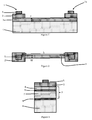
- MIM type capacitors 1 are planar capacitors, conventionally formed by a layer of perovskite-type material 2 disposed between a so-called lower electrode 3, in contact with a substrate 4, and a so-called upper electrode 5.
- a crystallization annealing at high temperature (at a temperature above 600 ° C) and under an oxidizing atmosphere is therefore generally performed after the formation of the perovskite type material on the lower electrode.
- the physical properties of the lower electrode should not be impaired during annealing.
- the lower electrode is conventionally made of platinum.
- MIM capacitors 1, 1a are generally deposited on the same substrate 4, for example in oxidized silicon, and are interconnected by a common lower electrode 3. They can also be connected to other components via this lower electrode which acts as a contact.
- the platinum lower electrode represents a parasitic line resistance that can be detrimental to the performance of the final product. It is therefore essential to reduce the line resistance significantly, to facilitate its introduction into a larger number of applications.
- the object of the invention is to remedy at least in part the drawbacks of the prior art and, in particular, to propose an electrode having a low resistivity.
- the parameters L and W of the patterns of the lines of the device are set for a given technology by drawing rules.
- the electrically conductive line connecting a capacitor to another element is formed by the lower electrode of the capacitor, that is to say by a platinum line.
- the lower electrode 3 is formed of a stack comprising a gold layer 7 and a platinum layer 6.
- the platinum layer has a thickness of between 80 nm and 120 nm.
- the platinum layer 6 has a thickness of about 100 nm and the thickness of the gold layer 7 will be adapted by those skilled in the art to obtain the desired line resistivity.
- the gold layer advantageously has a thickness of between 500 nm and 2 ⁇ m.
- Such a platinum thickness leads to a good crystallization of the perovskite-type dielectric material during annealing and, at the same time, this thickness remains sufficiently low (much less than 5 ⁇ m ) to avoid mechanical stresses (separation of the layer, etc. ) and not to increase production costs.
- a gold layer 7 having a thickness of about 1 ⁇ m is added to reduce the resistivity of the same electrode by a factor of 100.
- the gold layer 7 will have a thickness of 2 ⁇ m .
- the thickness of the gold layer 7 is advantageously less than 5 ⁇ m to avoid delamination, and preferably the gold layer 7 has a thickness ranging from 1 ⁇ m to 2 ⁇ m .
- the following table gives the resistances R of different electrodes before and after annealing at 700 ° C. under oxygen to recrystallize the perovskite-type dielectric material. stacking R before annealing ( ⁇ ) R after annealing ( ⁇ ) Pt (100 nm) 1.5 1.42 Cu (1 ⁇ m) / Pt (100nm) 0,019 insulating At (1 ⁇ m) / Pt (100nm) 0,028 0,144
- the line resistances of the Pt / metal electrodes are at least a factor of 50 less than those of the line resistance of a platinum electrode.
- the inventors have observed that, during the annealing in the presence of oxygen, the copper oxidizes and becomes insulating, and the gold diffuses into platinum, forming a gold-platinum alloy.
- the gain in resistivity is only a factor of 10 compared to the resistivity of a platinum line.
- barrier layer 8 not only prevents interdiffusion of platinum and gold, but also makes it possible to obtain a lower line resistance after annealing.
- barrier layer is meant a thin layer that can prevent the interdiffusion of two metals, in particular, here it is the diffusion of gold in platinum.
- the oxide is, advantageously, a noble metal oxide. It is selected from ruthenium oxide or any oxide of a noble metal such as platinum oxide, or preferentially iridium oxide.
- a ruthenium oxide layer is advantageously easy to produce and resists high temperature treatment under an oxidizing atmosphere.
- the electrode according to the invention for a metal-insulator-metal structure, is formed of a stack successively comprising a gold layer 7, a ruthenium oxide barrier layer 8 and a platinum layer 6 ( figure 3 ).
- the following table gives the resistances R of the different electrodes before and after annealing at 700 ° C. under oxygen. stacking R before annealing ( ⁇ ) R after annealing ( ⁇ ) Pt (100 nm) 1.5 1.42 At (1 ⁇ m) / Pt (100nm) 0,028 0,144 Au (1 ⁇ m) / WN (10nm) / Pt (100nm) 0,036 0.068 Au (1 ⁇ m) / RuO 2 (60nm) / Pt (100nm) 0.031 0.0241
- the resistance of the electrode increases after annealing.
- the platinum layer of the electrode has defects (holes, bumps). These defects seem to come from the oxidation of WN, during annealing, which leads to the formation of WO 3 and N 2 and a gas evolution through the platinum layer.
- the Au / RuO 2 / Pt stack is thermally and chemically stable. Even with thermal annealing, there is no delamination or diffusion between gold and platinum. As illustrated on the figure 5 the layers obtained are of very good quality. There are no surface defects.
- Ruthenium oxide forms an excellent diffusion barrier.
- a barrier layer of ruthenium oxide can be used as a barrier layer even at high temperature (at least 700 ° C) and under an oxidizing atmosphere.
- the line resistance of the Au / RuO 2 / Pt electrode, after annealing, is 50 times lower than that of a platinum electrode.
- the line resistance of such an electrode decreases after annealing. This decrease can be due to a better quality of the layers, and their recrystallization during the heat treatment.
- the thin layer of ruthenium oxide 8 has a thickness greater than or equal to 15 nm. As shown on the figure 6 a ruthenium oxide layer 8 with such a thickness forms a diffusion barrier sufficient for annealing at 700 ° C. Gold does not diffuse in platinum.
- the ruthenium oxide thin film 8 has a thickness greater than or equal to 40 nm and, even more preferably, greater than or equal to 80 nm. These thicknesses allow recrystallization annealing up to 800 ° C. The thicker the barrier layer is, the more effective the barrier layer is at higher temperatures. For example, for a thickness of 80 nm, it is possible to anneal up to 850 ° C for 60 seconds without the gold diffusing into the platinum. The duration of the anneals is between 15 seconds and 10 minutes, and preferably between 30 seconds and 5 minutes.
- the electrode 3 is disposed on a substrate 4 ( figure 3 ).
- the gold layer 7 of the electrode 3 is separated from the substrate 4 by a tie layer 9 based on titanium dioxide. This attachment layer 9 promotes the adhesion of the gold layer 7 to the substrate.
- the bonding layer is based on titanium dioxide, it is meant that the bonding layer is titanium dioxide or that the bonding layer is a TiO 2 / metal bilayer, the TiO 2 being in contact with the first electrode.
- the metal is selected from metals having good adhesion to silicon oxide, in particular.
- the metal may be selected from titanium, chromium or tantalum. This is, preferably, a two-layer TiO 2 / Ti.
- the tie layer between a gold layer and a substrate is generally made of titanium.
- a titanium tie layer 9 led to the diffusion of gold to the platinum layer despite the presence of the barrier layer 8 in RuO 2 .
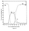
- the curve of the figure 7 represents an Auger profile through the electrode, from the platinum layer 6 to the titanium bonding layer 9, after annealing.
- the titanium diffuses to the barrier layer 8 in RuO 2 , with which it reacts to form ruthenium and titanium dioxide, which degrades the properties of the barrier layer 8 and leads to the diffusion of gold in the platinum .
- the barrier layer 8 of ruthenium dioxide is integrated ( figure 8 ).
- the gold does not diffuse in the platinum layer 6.
- the line resistance of the electrode 3 is weak.
- the first electrode 3 is disposed on a substrate 4.
- the substrate is intrinsically electrically insulating.
- the substrate is, for example, glass.
- the substrate could also be of polymer.
- the substrate 4 is electrically conductive or semiconductor.
- the surface of the substrate 4 is advantageously covered by a layer of electrically insulating material, called the insulation layer, in order to isolate the MIM structure 1 from said substrate 4.
- the electrically insulating material is, advantageously, an electrically insulating oxide, such as, for example, silicon oxide. According to another alternative, it may be a silicon nitride or a tantalum oxide.
- the insulation layer has a thickness of a few nanometers, or even a few tens of nanometers.
- the substrate is, for example, silicon or germanium, and is covered by an electrically insulating oxide layer.
- the substrate 4 is advantageously made of oxidized silicon.
- An adhesion layer 9 based on titanium dioxide is advantageously disposed between the first electrode 3 and the substrate 4, or between the first electrode 3 and the electrically insulating layer if the substrate 4 is electrically conductive.
- the dielectric material of the capacitance has a high dielectric constant. By high is meant at least 500.
- the perovskite dielectric material is electrically insulating.
- the perovskite type dielectric material is an oxide, advantageously chosen from Pb [Zr ⁇ Ti 1-x ] O 3 (PZT), SrTiO 3 (STO), BaTiO 3 (BTO), Ba [Sr ⁇ Ti 1-x ] O 3 (BST).
- the temperature of the heat treatment is advantageously greater than or equal to 700 ° C.
- the temperature of the heat treatment is greater than or equal to 850 ° C in order to crystallize the layer of perovskite-type dielectric material 2 well.
- the titanium dioxide can be obtained by oxidation of a titanium layer deposited on the silicon oxide.
- the inventors have observed that the deposition of a titanium layer which is subsequently oxidized provides better results than the deposition of a titanium dioxide layer. This allows a better adhesion of noble metals such as gold on a silicon oxide layer.
- a titanium layer having a thickness of 10 nm followed by an oxidation step at the temperature of 750 ° C. under an atmosphere comprising or consisting of oxygen.
- the operating conditions are advantageously defined to achieve the complete oxidation of titanium dioxide titanium dioxide, the duration of the oxidation step is for example equal to 5 minutes.
- the thickness of the titanium layer may be between 5 nm and 50 nm or between 5 nm and 20 nm.
- the deposition of the titanium layer may be carried out at a temperature above 200 ° C, for example between 200 ° C and 400 ° C. It is also possible to provide that the oxidation of the titanium layer can be carried out at a temperature above 500 ° C. The duration of the annealing step is adjusted to achieve complete oxidation of the titanium layer.
- the lower electrode formed during step b) is produced by successive deposits of gold, ruthenium oxide, and platinum by sputtering. The electrode is then etched to have the desired pattern.
- the dielectric material PZT is deposited by sol-gel (step c)), by spin coating (or “spin-coating”). The deposit is then dried for a few minutes at a hundred degrees. A layer of PZT of about 200 nm is obtained.
- the crystallization annealing (step d)) is carried out at 700 ° C. under O 2 for 60 seconds.
- a platinum top electrode is deposited by sputtering.
- the upper electrode has a thickness of about 100 nm.
- the electrodes have a low line resistance.
- the line resistance is a factor of 50 lower than conventional platinum electrodes. Capacities containing such electrodes are particularly interesting for high frequency applications.
Landscapes
- Semiconductor Memories (AREA)
- Semiconductor Integrated Circuits (AREA)
- Fixed Capacitors And Capacitor Manufacturing Machines (AREA)
Applications Claiming Priority (1)
| Application Number | Priority Date | Filing Date | Title |
|---|---|---|---|
| FR1557206A FR3039704B1 (fr) | 2015-07-28 | 2015-07-28 | Electrode pour structure metal-isolant-metal, capacite de type metal-isolant-metal, et procede de realisation d’une telle electrode et d’une telle capacite. |
Publications (2)
| Publication Number | Publication Date |
|---|---|
| EP3125293A2 true EP3125293A2 (de) | 2017-02-01 |
| EP3125293A3 EP3125293A3 (de) | 2017-04-05 |
Family
ID=54366341
Family Applications (1)
| Application Number | Title | Priority Date | Filing Date |
|---|---|---|---|
| EP16181598.0A Pending EP3125293A3 (de) | 2015-07-28 | 2016-07-28 | Elektrode für metall-isolator-metall-struktur, kapazität vom typ metall-isolator-metall und herstellungsverfahren einer solchen elektrode und einer solchen kapazität |
Country Status (3)
| Country | Link |
|---|---|
| US (1) | US10319806B2 (de) |
| EP (1) | EP3125293A3 (de) |
| FR (1) | FR3039704B1 (de) |
Cited By (1)
| Publication number | Priority date | Publication date | Assignee | Title |
|---|---|---|---|---|
| EP3588595A1 (de) | 2018-06-22 | 2020-01-01 | Commissariat à l'énergie atomique et aux énergies alternatives | Mim-struktur und herstellungsverfahren dafür |
Families Citing this family (3)
| Publication number | Priority date | Publication date | Assignee | Title |
|---|---|---|---|---|
| EP4216245A3 (de) | 2022-01-19 | 2023-11-22 | Samsung Electronics Co., Ltd. | Kondensator, halbleiterbauelement mit dem kondensator und verfahren zur herstellung des kondensators |
| US12543323B2 (en) * | 2022-02-02 | 2026-02-03 | Taiwan Semiconductor Manufacturing Company, Ltd. | Ferroelectric memory device with relaxation layers |
| FR3148496A1 (fr) | 2023-05-04 | 2024-11-08 | Commissariat A L'energie Atomique Et Aux Energies Alternatives | Structure comprenant deux couches de nature électrique différente et son procédé de préparation |
Family Cites Families (14)
| Publication number | Priority date | Publication date | Assignee | Title |
|---|---|---|---|---|
| JP2000349254A (ja) * | 1999-06-02 | 2000-12-15 | Sony Corp | 誘電体キャパシタおよびメモリならびにそれらの製造方法 |
| US6485988B2 (en) * | 1999-12-22 | 2002-11-26 | Texas Instruments Incorporated | Hydrogen-free contact etch for ferroelectric capacitor formation |
| US6887716B2 (en) * | 2000-12-20 | 2005-05-03 | Fujitsu Limited | Process for producing high quality PZT films for ferroelectric memory integrated circuits |
| JP4682657B2 (ja) * | 2005-03-22 | 2011-05-11 | パナソニック株式会社 | 弾性表面波デバイス |
| US20110250402A1 (en) * | 2008-06-02 | 2011-10-13 | Applied Biosystems, Llc | Localization of near-field resonances in bowtie antennae: influence of adhesion layers |
| JP2010177257A (ja) * | 2009-01-27 | 2010-08-12 | Panasonic Corp | 半導体装置及びその製造方法 |
| JP2010278074A (ja) * | 2009-05-26 | 2010-12-09 | Fujitsu Semiconductor Ltd | 電子装置およびその製造方法 |
| JP5596312B2 (ja) * | 2009-08-04 | 2014-09-24 | スタンレー電気株式会社 | 誘電体薄膜デバイスの製造方法 |
| WO2012066803A1 (ja) * | 2010-11-16 | 2012-05-24 | 三菱電機株式会社 | 半導体素子、半導体装置及び半導体素子の製造方法 |
| EP2852989B1 (de) * | 2012-07-31 | 2016-11-30 | Hewlett-Packard Development Company, L.P. | Dünnschichtstapel |
| JP6287278B2 (ja) * | 2014-02-03 | 2018-03-07 | 富士通セミコンダクター株式会社 | 半導体装置及びその製造方法 |
| US9502647B2 (en) * | 2014-05-28 | 2016-11-22 | Taiwan Semiconductor Manufacturing Company Limited | Resistive random-access memory (RRAM) with a low-K porous layer |
| US9653613B2 (en) * | 2015-02-27 | 2017-05-16 | Semiconductor Energy Laboratory Co., Ltd. | Semiconductor device and manufacturing method thereof |
| US9871107B2 (en) * | 2015-05-22 | 2018-01-16 | Nxp Usa, Inc. | Device with a conductive feature formed over a cavity and method therefor |
-
2015
- 2015-07-28 FR FR1557206A patent/FR3039704B1/fr active Active
-
2016
- 2016-07-27 US US15/220,869 patent/US10319806B2/en active Active
- 2016-07-28 EP EP16181598.0A patent/EP3125293A3/de active Pending
Non-Patent Citations (1)
| Title |
|---|
| C. H. JOHANSSON; J. O. LINDE: "Rontgenographische und elektrische Untersuchungen des CuAu-Systems", ANNALEN DER PHYSIK, vol. 25, 1936, pages 1 - 48 |
Cited By (2)
| Publication number | Priority date | Publication date | Assignee | Title |
|---|---|---|---|---|
| EP3588595A1 (de) | 2018-06-22 | 2020-01-01 | Commissariat à l'énergie atomique et aux énergies alternatives | Mim-struktur und herstellungsverfahren dafür |
| US11417723B2 (en) | 2018-06-22 | 2022-08-16 | Commissariat A L'energie Atomique Et Aux Energies Alternatives | Metal-insulator metal structure and method of forming the same |
Also Published As
| Publication number | Publication date |
|---|---|
| US10319806B2 (en) | 2019-06-11 |
| FR3039704A1 (fr) | 2017-02-03 |
| US20170033174A1 (en) | 2017-02-02 |
| EP3125293A3 (de) | 2017-04-05 |
| FR3039704B1 (fr) | 2017-12-29 |
Similar Documents
| Publication | Publication Date | Title |
|---|---|---|
| KR100314489B1 (ko) | 강유전체 커패시터의 간단한 제조방법 | |
| EP2080204B1 (de) | Hochstabiler dünnfilmkondensator und verfahren zu seiner herstellung | |
| FR2678766A1 (fr) | Condensateur a constante dielectrique elevee et procede pour sa fabrication. | |
| EP3796390B1 (de) | Mikroelektronische vorrichtung mit einer nichtklonierbaren physischen funktion, die durch resistive speicher bereitgestellt wird, und herstellungsverfahren dafür | |
| EP3125293A2 (de) | Elektrode für metall-isolator-metall-struktur, kapazität vom typ metall-isolator-metall und herstellungsverfahren einer solchen elektrode und einer solchen kapazität | |
| US20130094120A1 (en) | Thin-film capacitor | |
| EP1351315A2 (de) | Elektronische Mikrokomponente mit integrierter Kondensator-Struktur und diesbezügliches Herstellungsverfahren | |
| EP2680287B1 (de) | Anordnung für Superkondensatorvorrichtung, Superkondensatorvorrichtung, die eine solche Anordnung umfasst, und Herstellungsverfahren einer solchen Anordnung | |
| EP3588595A1 (de) | Mim-struktur und herstellungsverfahren dafür | |
| KR20000071417A (ko) | 이리듐 도전성 전극/배리어 구조 및 그의 제조 방법 | |
| EP3591724B1 (de) | Verfahren zur realisierung einer piezoelektrischen wandlervorrichtung | |
| EP3587343A1 (de) | Herstellungsverfahren einer vorrichtung, die zumindest teilweise transparent ist und eine struktur vom typ kondensator umfasst | |
| US20020030243A1 (en) | Semiconductor device and method for fabricating the same | |
| US20080157278A1 (en) | Semiconductor device and method for fabricating the same | |
| EP1351314A2 (de) | Elektronische Mikrokomponente mit Kondensator und diesbezügliches Herstellungsverfahren | |
| EP2530755B1 (de) | Elektrisches Bauteil umfassend ein Material mit einer Perowskitstruktur und optimierte Elektroden sowie entsprechendes Herstellungverfahren | |
| FR2801425A1 (fr) | Capacite integree a dielectrique hybride | |
| JPH04287968A (ja) | 集積回路装置およびその製造方法 | |
| EP4572593B1 (de) | Verfahren zur herstellung einer speichervorrichtung und eine speichervorrichtung | |
| KR100437071B1 (ko) | Fram 및 dram용 고온 전극 및 배리어 구조 | |
| EP3984073B1 (de) | Verfahren zur herstellung einer resistiven oxram-speicherzelle | |
| EP1686598A1 (de) | Kondensator mit erhöhter Durchschlagsfeldstärke | |
| FR2907593A1 (fr) | Procede de fabrication d'un condensateur a stabilite elevee. | |
| FR2837623A1 (fr) | Micro-composant electronique integrant une structure capacitive, et procede de fabrication | |
| FR2837624A1 (fr) | Micro-composant electronique integrant une structure capacitive, et procede de fabrication |
Legal Events
| Date | Code | Title | Description |
|---|---|---|---|
| PUAI | Public reference made under article 153(3) epc to a published international application that has entered the european phase |
Free format text: ORIGINAL CODE: 0009012 |
|
| STAA | Information on the status of an ep patent application or granted ep patent |
Free format text: STATUS: THE APPLICATION HAS BEEN PUBLISHED |
|
| AK | Designated contracting states |
Kind code of ref document: A2 Designated state(s): AL AT BE BG CH CY CZ DE DK EE ES FI FR GB GR HR HU IE IS IT LI LT LU LV MC MK MT NL NO PL PT RO RS SE SI SK SM TR |
|
| AX | Request for extension of the european patent |
Extension state: BA ME |
|
| PUAL | Search report despatched |
Free format text: ORIGINAL CODE: 0009013 |
|
| AK | Designated contracting states |
Kind code of ref document: A3 Designated state(s): AL AT BE BG CH CY CZ DE DK EE ES FI FR GB GR HR HU IE IS IT LI LT LU LV MC MK MT NL NO PL PT RO RS SE SI SK SM TR |
|
| AX | Request for extension of the european patent |
Extension state: BA ME |
|
| RIC1 | Information provided on ipc code assigned before grant |
Ipc: H01L 27/108 20060101AFI20170302BHEP Ipc: H01L 49/02 20060101ALI20170302BHEP |
|
| STAA | Information on the status of an ep patent application or granted ep patent |
Free format text: STATUS: REQUEST FOR EXAMINATION WAS MADE |
|
| 17P | Request for examination filed |
Effective date: 20170414 |
|
| RBV | Designated contracting states (corrected) |
Designated state(s): AL AT BE BG CH CY CZ DE DK EE ES FI FR GB GR HR HU IE IS IT LI LT LU LV MC MK MT NL NO PL PT RO RS SE SI SK SM TR |
|
| STAA | Information on the status of an ep patent application or granted ep patent |
Free format text: STATUS: EXAMINATION IS IN PROGRESS |
|
| 17Q | First examination report despatched |
Effective date: 20181114 |
|
| STAA | Information on the status of an ep patent application or granted ep patent |
Free format text: STATUS: THE APPLICATION IS DEEMED TO BE WITHDRAWN |
|
| 18D | Application deemed to be withdrawn |
Effective date: 20210925 |
|
| 18RA | Request filed for re-establishment of rights before grant |
Effective date: 20220920 |
|
| 18RR | Decision to grant the request for re-establishment of rights before grant |
Free format text: ANGENOMMEN Effective date: 20230124 |
|
| 18RA | Request filed for re-establishment of rights before grant |
Effective date: 20220920 |
|
| 18RR | Decision to grant the request for re-establishment of rights before grant |
Free format text: ANGENOMMEN Effective date: 20230124 |
|
| STAA | Information on the status of an ep patent application or granted ep patent |
Free format text: STATUS: EXAMINATION IS IN PROGRESS |
|
| D18D | Application deemed to be withdrawn (deleted) | ||
| RAP3 | Party data changed (applicant data changed or rights of an application transferred) |
Owner name: STMICROELECTRONICS (CROLLES 2) SAS Owner name: COMMISSARIAT A L'ENERGIE ATOMIQUE ET AUX ENERGIESALTERNATIVES |
|
| REG | Reference to a national code |
Ref country code: DE Ref legal event code: R079 Free format text: PREVIOUS MAIN CLASS: H01L0027108000 Ipc: H10D0001680000 |
|
| RIC1 | Information provided on ipc code assigned before grant |
Ipc: H10D 1/68 20250101AFI20251209BHEP |
|
| GRAP | Despatch of communication of intention to grant a patent |
Free format text: ORIGINAL CODE: EPIDOSNIGR1 |
|
| STAA | Information on the status of an ep patent application or granted ep patent |
Free format text: STATUS: GRANT OF PATENT IS INTENDED |
|
| INTG | Intention to grant announced |
Effective date: 20260127 |