EP3123508B1 - Inductor embedded in a package subtrate - Google Patents
Inductor embedded in a package subtrate Download PDFInfo
- Publication number
- EP3123508B1 EP3123508B1 EP15715112.7A EP15715112A EP3123508B1 EP 3123508 B1 EP3123508 B1 EP 3123508B1 EP 15715112 A EP15715112 A EP 15715112A EP 3123508 B1 EP3123508 B1 EP 3123508B1
- Authority
- EP
- European Patent Office
- Prior art keywords
- inductor
- package substrate
- dielectric layer
- coupled
- pad
- Prior art date
- Legal status (The legal status is an assumption and is not a legal conclusion. Google has not performed a legal analysis and makes no representation as to the accuracy of the status listed.)
- Active
Links
Images


Classifications
-
- H—ELECTRICITY
- H01—ELECTRIC ELEMENTS
- H01F—MAGNETS; INDUCTANCES; TRANSFORMERS; SELECTION OF MATERIALS FOR THEIR MAGNETIC PROPERTIES
- H01F17/00—Fixed inductances of the signal type
- H01F17/0006—Printed inductances
- H01F17/0013—Printed inductances with stacked layers
-
- H—ELECTRICITY
- H01—ELECTRIC ELEMENTS
- H01L—SEMICONDUCTOR DEVICES NOT COVERED BY CLASS H10
- H01L23/00—Details of semiconductor or other solid state devices
- H01L23/48—Arrangements for conducting electric current to or from the solid state body in operation, e.g. leads, terminal arrangements ; Selection of materials therefor
- H01L23/488—Arrangements for conducting electric current to or from the solid state body in operation, e.g. leads, terminal arrangements ; Selection of materials therefor consisting of soldered or bonded constructions
- H01L23/498—Leads, i.e. metallisations or lead-frames on insulating substrates, e.g. chip carriers
- H01L23/49822—Multilayer substrates
-
- H—ELECTRICITY
- H01—ELECTRIC ELEMENTS
- H01L—SEMICONDUCTOR DEVICES NOT COVERED BY CLASS H10
- H01L23/00—Details of semiconductor or other solid state devices
- H01L23/52—Arrangements for conducting electric current within the device in operation from one component to another, i.e. interconnections, e.g. wires, lead frames
- H01L23/538—Arrangements for conducting electric current within the device in operation from one component to another, i.e. interconnections, e.g. wires, lead frames the interconnection structure between a plurality of semiconductor chips being formed on, or in, insulating substrates
- H01L23/5383—Multilayer substrates
-
- H—ELECTRICITY
- H10—SEMICONDUCTOR DEVICES; ELECTRIC SOLID-STATE DEVICES NOT OTHERWISE PROVIDED FOR
- H10D—INORGANIC ELECTRIC SEMICONDUCTOR DEVICES
- H10D1/00—Resistors, capacitors or inductors
- H10D1/20—Inductors
-
- H—ELECTRICITY
- H01—ELECTRIC ELEMENTS
- H01F—MAGNETS; INDUCTANCES; TRANSFORMERS; SELECTION OF MATERIALS FOR THEIR MAGNETIC PROPERTIES
- H01F17/00—Fixed inductances of the signal type
- H01F17/0006—Printed inductances
- H01F17/0013—Printed inductances with stacked layers
- H01F2017/002—Details of via holes for interconnecting the layers
-
- H—ELECTRICITY
- H01—ELECTRIC ELEMENTS
- H01F—MAGNETS; INDUCTANCES; TRANSFORMERS; SELECTION OF MATERIALS FOR THEIR MAGNETIC PROPERTIES
- H01F17/00—Fixed inductances of the signal type
- H01F17/0006—Printed inductances
- H01F2017/0066—Printed inductances with a magnetic layer
-
- H—ELECTRICITY
- H01—ELECTRIC ELEMENTS
- H01L—SEMICONDUCTOR DEVICES NOT COVERED BY CLASS H10
- H01L2224/00—Indexing scheme for arrangements for connecting or disconnecting semiconductor or solid-state bodies and methods related thereto as covered by H01L24/00
- H01L2224/01—Means for bonding being attached to, or being formed on, the surface to be connected, e.g. chip-to-package, die-attach, "first-level" interconnects; Manufacturing methods related thereto
- H01L2224/10—Bump connectors; Manufacturing methods related thereto
- H01L2224/15—Structure, shape, material or disposition of the bump connectors after the connecting process
- H01L2224/16—Structure, shape, material or disposition of the bump connectors after the connecting process of an individual bump connector
- H01L2224/161—Disposition
- H01L2224/16151—Disposition the bump connector connecting between a semiconductor or solid-state body and an item not being a semiconductor or solid-state body, e.g. chip-to-substrate, chip-to-passive
- H01L2224/16221—Disposition the bump connector connecting between a semiconductor or solid-state body and an item not being a semiconductor or solid-state body, e.g. chip-to-substrate, chip-to-passive the body and the item being stacked
- H01L2224/16225—Disposition the bump connector connecting between a semiconductor or solid-state body and an item not being a semiconductor or solid-state body, e.g. chip-to-substrate, chip-to-passive the body and the item being stacked the item being non-metallic, e.g. insulating substrate with or without metallisation
-
- H—ELECTRICITY
- H01—ELECTRIC ELEMENTS
- H01L—SEMICONDUCTOR DEVICES NOT COVERED BY CLASS H10
- H01L23/00—Details of semiconductor or other solid state devices
- H01L23/48—Arrangements for conducting electric current to or from the solid state body in operation, e.g. leads, terminal arrangements ; Selection of materials therefor
- H01L23/488—Arrangements for conducting electric current to or from the solid state body in operation, e.g. leads, terminal arrangements ; Selection of materials therefor consisting of soldered or bonded constructions
- H01L23/498—Leads, i.e. metallisations or lead-frames on insulating substrates, e.g. chip carriers
- H01L23/49827—Via connections through the substrates, e.g. pins going through the substrate, coaxial cables
-
- H—ELECTRICITY
- H01—ELECTRIC ELEMENTS
- H01L—SEMICONDUCTOR DEVICES NOT COVERED BY CLASS H10
- H01L23/00—Details of semiconductor or other solid state devices
- H01L23/58—Structural electrical arrangements for semiconductor devices not otherwise provided for, e.g. in combination with batteries
- H01L23/64—Impedance arrangements
- H01L23/645—Inductive arrangements
-
- H—ELECTRICITY
- H01—ELECTRIC ELEMENTS
- H01L—SEMICONDUCTOR DEVICES NOT COVERED BY CLASS H10
- H01L2924/00—Indexing scheme for arrangements or methods for connecting or disconnecting semiconductor or solid-state bodies as covered by H01L24/00
- H01L2924/10—Details of semiconductor or other solid state devices to be connected
- H01L2924/11—Device type
- H01L2924/14—Integrated circuits
-
- H—ELECTRICITY
- H01—ELECTRIC ELEMENTS
- H01L—SEMICONDUCTOR DEVICES NOT COVERED BY CLASS H10
- H01L2924/00—Indexing scheme for arrangements or methods for connecting or disconnecting semiconductor or solid-state bodies as covered by H01L24/00
- H01L2924/15—Details of package parts other than the semiconductor or other solid state devices to be connected
- H01L2924/151—Die mounting substrate
- H01L2924/153—Connection portion
- H01L2924/1531—Connection portion the connection portion being formed only on the surface of the substrate opposite to the die mounting surface
- H01L2924/15311—Connection portion the connection portion being formed only on the surface of the substrate opposite to the die mounting surface being a ball array, e.g. BGA
-
- H—ELECTRICITY
- H01—ELECTRIC ELEMENTS
- H01L—SEMICONDUCTOR DEVICES NOT COVERED BY CLASS H10
- H01L2924/00—Indexing scheme for arrangements or methods for connecting or disconnecting semiconductor or solid-state bodies as covered by H01L24/00
- H01L2924/30—Technical effects
- H01L2924/301—Electrical effects
- H01L2924/3011—Impedance
Definitions
- Various features relate to an inductor embedded in a package substrate.
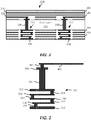
- FIG. 1 illustrates a conventional integrated package 100 that includes a substrate 102, a set of interconnects 104, a first die 106, a second die 108, a first set of solder balls 116, a second set of solder balls 118, and a third set of solder balls 120.
- the set of interconnects 104 includes traces and vias, which are located inside the substrate 102.
- the first die 106 is coupled to the substrate 102 through the first set of solder balls 116.
- the second die 108 is coupled to the substrate 102 through the second set of solder balls 118.
- the third set of solder balls 120 is coupled to the substrate 102.
- the first die 106 and the second die 108 are coupled to the third set of solder balls 120 through the set of interconnects 104.
- the third set of solder balls 120 is coupled to a printed circuit board (PCB) (not shown).
- PCB printed circuit board
- the set of interconnects 104 may have certain impedance values which do not match or closely match with the impedance values of the third set of solder balls 120.
- This mismatch in impedance values can cause signal loss or signal degradation, which affects the overall performance of the package substrate, and ultimately the performance of the integrated device that includes the package substrate. Similar results (e.g., mismatch in impedance values) may occur when using landing pads instead of solder balls.
- the mismatch in impedance values is because of the size difference between the size of the set of interconnects 104 and the size of the third set of solder balls 120.
- solder balls are substantially bigger than an interconnect (e.g., trace, via) in a package substrate.
- interconnect e.g., trace, via
- a package substrate according to claim 1 and a method for fabricating a package substrate according to claim 9 are provided. Additional aspects are provided according to the dependent claims.
- a package substrate that includes a core layer, a first via (e.g., first pin), a first dielectric layer, and a first inductor.
- the core layer includes a first surface and a second surface.
- the first via is located in the core layer.
- the first dielectric layer is coupled to the first surface of the core layer.
- the first inductor is located in the first dielectric layer.
- the first inductor is coupled to the first via in the core layer.
- the first inductor is configured to generate a magnetic field that laterally traverses the package substrate.
- the package substrate further includes a first pad coupled to the first inductor, wherein the first pad is configured to couple to a solder ball.
- the first inductor includes a first set of vias, and a first set of interconnects.
- the package substrate includes a second via (e.g., second pin) located in the core layer, and a second inductor located in the first dielectric layer, wherein the second inductor coupled to the second via in the core layer.
- the first inductor is positioned in the first dielectric layer such that the magnetic field that is generated by the first inductor affects the impedance of a pad coupled to the second inductor.
- FIG. 2 conceptually illustrates an example a package substrate that includes an inductor. Specifically, FIG. 2 illustrates a package substrate 200 that includes a core layer 202, a first dielectric layer 204, and a second dielectric layer 206.
- the first dielectric layer 204 may include several dielectric layers.
- the second dielectric layer 206 may include several dielectric layers.
- the core layer 202 includes a first via 220 and a second via 230.
- the first via 220 and/or the second via 230 may be a pin.
- the first dielectric layer 204 includes a first set of interconnects 214, a first inductor 222, a first pad 224, a second inductor 232, and a second pad 234.
- the second dielectric layer 206 includes a second set of interconnects 216, a third set of interconnects 226, and a fourth set of interconnects 236.
- the first inductor 222 includes several interconnects (e.g., traces, vias, pads), which are configured to provide a set of windings for the first inductor 222.
- a first portion (e.g., top portion) of the first inductor 222 is coupled to a first portion (e.g., bottom portion) of the first via 220.
- a second portion (e.g., bottom portion) of the first inductor 222 is coupled to the first pad 224.
- the first pad 224 is configured to couple to a set of solder balls.
- a signal interconnect may include one of at least a via (e.g., first via 220) in the core layer 202 and/or a set of interconnects (e.g., fourth set of interconnects 236) in the second dielectric layer 206.
- the signal interconnect may include the inductor 222 and/or the inductor 232.
- an interconnect may include a trace.
- matching the impedance or reducing the difference between the impedance of a signal interconnect and the pad(s) provides better signal performance.
- matching the impedance or reducing the impedance difference reduces signal loss and/or signal degradation between the pad and signal interconnect, thereby providing better signal performance for the package substrate.
- a second portion (e.g., top portion) of the first via 220 is coupled to the third set of interconnects 226.
- the third set of interconnects 226 are located in the second dielectric layer 206.
- the third set of interconnects 226 may include traces and/or vias.
- the second inductor 232 includes several interconnects (e.g., traces, vias, pads), which are configured to provide a set of windings for the second inductor 232.
- a first portion (e.g., top portion) of the second inductor 232 is coupled to a first portion (e.g., bottom portion) of the second via 230.
- a second portion (e.g., bottom portion) of the second inductor 232 is coupled to the second pad 234.
- the second pad 234 is configured to couple to a set of solder balls.
- the second inductor 232 is configured in such a way that the impedance of the second pad 234 matches or closely matches the impedance of the signal interconnect to which the second pad 234 will be coupled to.
- a second portion (e.g., top portion) of the second via 230 is coupled to the fourth set of interconnects 236.
- the fourth set of interconnects 236 are located in the second dielectric layer 206.
- the fourth set of interconnects 236 may includes traces and/or vias.
- FIG. 3 illustrates a close up view of a set of interconnects in a package substrate, where some of the set of interconnects are configured to operate as an inductor. For purpose of clarity, the package substrate is not shown in FIG. 3 .
- FIG. 3 illustrates a first trace 302 coupled to a first via 304.
- the first via 304 is coupled to a pad 306.
- the first trace 302, the first via 304, and the first pad 306 are located in a first dielectric layer (e.g., dielectric layer 206) of a package substrate (e.g., package substrate 200).
- the first pad 306 is coupled to a first portion (e.g., top portion) of the first via 308.
- the first via 308 is a pin.
- the first via 308 is located in a core layer (e.g., core layer 202) of a package substrate.
- a second portion (e.g., bottom portion) of the first via 308 is coupled to a first inductor 310.
- the first inductor 310 is located in a second dielectric layer (e.g., dielectric layer 204) of a package substrate.
- the first inductor 310 includes a second pad 312, a second via 313, a second trace 314, a third via 315, a third trace 316, a fourth via 317, a fourth trace 318, and a fifth via 319.
- the second pad 312 is coupled to the second portion of the first via 308.
- the second pad 312 is also coupled to the second via 313.
- the second via 313 is coupled to the second trace 314.
- the second trace 314 is coupled to the third via 315.
- the third via 315 is coupled to the third trace 316.
- the third trace 316 is coupled to the fourth via 317.
- the fourth via 317 is coupled the fourth trace 318.
- the fourth trace 318 is coupled to the fifth via 319.
- the fifth via 319 is coupled to the third pad 320.
- the third pad 320 is configured to couple to a solder ball or another pad (e.g., landing pad from landing pad array).
- the second pad 312, the second via 313, the second trace 314, the third via 315, the third trace 316, the fourth via 317, the fourth trace 318, and/or the fifth via 319 are configured to operate as a spiral winding for the first inductor 310.
- the third pad 320 is part of the first inductor 310. It should be noted that different implementations may have different numbers of traces and/or vias. Different configurations of the inductor will produce different magnetic fields along different directions. In some implementations, the strength and/or direction of the magnetic field generated by the inductor will affect the impedance of the pad (e.g., pad that is coupled to a solder ball) or the via (e.g., pin).
- the inductor is coupled to a signal interconnect.
- a signal interconnect may include one of at least a via (e.g., via 308), a pad (e.g., pad 306) and/or a trace (e.g., trace 302).
- the signal interconnect may include the inductor.
- FIG. 4 illustrates an example of a magnetic field that may be generated by an inductor in a package substrate.
- an inductor 400 generates a vertical magnetic field.
- the inductor 400 is similar to the inductors 222 and 232 of FIG. 2 , and/or the inductor 310 of FIG. 3 .
- the vertical magnetic field helps improve the impedance difference (e.g., reduce the impedance difference between a pad and a signal interconnect).
- the use of an inductor coupled to a via and a pad may reduce the impedance difference between a pad and a signal interconnect to 2.5 ohms or less.
- excess magnetic field resonates away excess electrical field created by a big pad, resulting in a pad with higher impedance which is closer to that of a signal interconnect.
- FIG. 5 illustrates an angled view of vias coupled to inductors.
- a package substrate is not shown, although the inductors shown in FIG. 5 may be implemented in a package substrate.
- a first via 500 is coupled to a first inductor 502.
- the first inductor 502 includes several interconnects (e.g., traces, vias, pads) which are configured to operate as a first spiral winding for the first inductor 502.
- the first inductor 502 is also coupled to a first pad 504.
- the first pad 504 may be configured to couple to a solder ball or a landing pad from a landing pad array.
- an inductor may be configured to produce a lateral magnetic field (e.g., magnetic field that laterally traverses a package substrate) in a package substrate, which may provide several technical advantages.
- a lateral magnetic field e.g., magnetic field that laterally traverses a package substrate
- FIG. 6 conceptually illustrates an example of a package substrate that includes an inductor that can produce a lateral magnetic field.
- FIG. 6 illustrates a package substrate 600 that includes a core layer 602, a first dielectric layer 604, and a second dielectric layer 606.
- the first dielectric layer 604 may include several dielectric layers.
- the second dielectric layer 606 may include several dielectric layers.
- the core layer 602 includes a first via 620 and a second via 630.
- the first via 620 and/or the second via 630 may be a pin.
- the first dielectric layer 604 includes a first set of interconnects 614, a first inductor 622, a first pad 624, a second inductor 632, and a second pad 634.
- the second dielectric layer 606 includes a second set of interconnects 616, a third set of interconnects 626, and a fourth set of interconnects 636.
- the first inductor 622 includes several interconnects (e.g., traces, vias, pads), which are configured to provide a set of windings for the first inductor 622.
- a first portion (e.g., top portion) of the first inductor 622 is coupled to a first portion (e.g., bottom portion) of the first via 620.
- a second portion (e.g., bottom portion) of the first inductor 622 is coupled to the first pad 624.
- the first pad 624 is configured to couple to a set of solder balls.
- the first inductor 622 is configured in such a way that the impedance of the first pad 624 matches or closely matches the impedance of the signal interconnect to which the first pad 624 will be coupled to.
- a signal interconnect may include one of at least a via (e.g., first via 620) in the core layer 602 and/or a set of interconnects (e.g., fourth set of interconnects 636) in the second dielectric layer 606.
- the signal interconnect may include the inductor 622 and/or the inductor 632.
- an interconnect may include a trace.
- the first inductor 622 may be configured to provide a magnetic field that laterally traverses the package substrate 600. A technical advantage and/or benefit of a magnetic field that laterally traverses a package substrate will be further described in FIGS. 8-9 .
- matching the impedance or reducing the difference between the impedance of the signal interconnect and the pads provides better signal performance.
- matching the impedance or reducing the impedance difference reduces signal loss and/or signal degradation between the pad and the signal interconnect, thereby providing better signal performance for the package substrate.
- a second portion (e.g., top portion) of the first via 620 is coupled to the third set of interconnects 626.
- the third set of interconnects 626 are located in the second dielectric layer 606.
- the third set of interconnects 626 may includes traces and/or vias.
- the second inductor 632 includes several interconnects (e.g., traces, vias, pads), which are configured to provide a set of windings for the second inductor 632.
- a first portion (e.g., top portion) of the second inductor 632 is coupled to a first portion (e.g., bottom portion) of the second via 630.
- a second portion (e.g., bottom portion) of the second inductor 632 is coupled to the second pad 634.
- the second pad 634 is configured to couple to a set of solder balls.
- the second inductor 632 is configured in such a way that the impedance of the second pad 634 matches or closely matches the impedance of the signal interconnect to which the second pad 634 will be coupled to.
- the second inductor 632 may be configured to provide a magnetic field that laterally traverses the package substrate 600. As mentioned above, a technical advantage and/or benefit of a magnetic field that laterally traverses a package substrate will be further described in FIGS. 8-9 .
- a second portion (e.g., top portion) of the second via 630 is coupled to the fourth set of interconnects 636.
- the fourth set of interconnects 636 are located in the second dielectric layer 606.
- the fourth set of interconnects 636 may includes traces and/or vias.
- FIG. 7 illustrates a close up view of a set of interconnects in a package substrate, where some of the set of interconnects are configured to operate as an inductor. For purpose of clarity, the package substrate is not shown in FIG. 7 .
- FIG. 7 illustrates a first trace 702 coupled to a first via 704.
- the first via 704 is coupled to a pad 706.
- the first trace 702, the first via 704, and the first pad 706 are located in a first dielectric layer (e.g., dielectric layer 606) of a package substrate (e.g., package substrate 600).
- the first pad 706 is coupled to a first portion (e.g., top portion) of the first via 708.
- the first via 708 is a first pin.
- the first via 708 is located in a core layer (e.g., core layer 602) of a package substrate.
- a second portion (e.g., bottom portion) of the first via 708 is coupled to a first inductor 710.
- the first inductor 710 is located in a second dielectric layer (e.g., dielectric layer 604) of a package substrate.
- the first inductor 710 includes a second pad 712, a second via 713, a second trace 714, a third via 715, a third trace 716, a fourth via 717, a fourth trace 718, and a fifth via 719.
- the second pad 712 is coupled to the second portion of the first via 708.
- the second pad 712 is also coupled to the second via 713.
- the second via 713 is coupled to the second trace 714.
- the second trace 714 is coupled to the third via 715.
- the third via 715 is coupled to the third trace 716.
- the third trace 716 is coupled to the fourth via 717.
- the fourth via 717 is coupled the fourth trace 718.
- the fourth trace 718 is coupled to the fifth via 719.
- the fifth via 719 is coupled to the third pad 720.
- the third pad 720 is configured to couple to a solder ball or another pad (e.g., landing pad from landing pad array).
- the second pad 712, the second via 713, the second trace 714, the third via 715, the third trace 716, the fourth via 717, the fourth trace 718, and/or the fifth via 719 are configured to operate as a spiral winding for the first inductor 710.
- the third pad 720 is part of the first inductor 710. It should be noted that different implementations may have different numbers of traces and/or vias. Different configurations of the inductor will produce different magnetic fields along different directions. In some implementations, the strength and/or direction of the magnetic field generated by the inductor will affect the impedance of the pad (e.g., pad that is coupled to a solder ball) or the via (e.g., pin).
- the inductor is coupled to a signal interconnect.
- a signal interconnect may include one of at least a via (e.g., via 708), a pad (e.g., pad 706) and/or a trace (e.g., trace 702).
- the signal interconnect includes the inductor.
- FIG. 8 illustrates an example of magnetic fields that may be generated by inductors in a package substrate.
- a first inductor 800 generates a lateral magnetic field that laterally traverses a package substrate
- a second inductor 802 generates a magnetic field that also laterally traverses the package substrate.
- the inductors 800 and 802 are similar to the inductors 622 and 632 of FIG. 6 , and/or the inductor 710 of FIG. 7 .
- the lateral magnetic field helps improve the impedance difference (e.g., reduce the impedance difference between a pad and a signal interconnect).
- the use of an inductor coupled to a via and a pad may reduce the impedance difference between a pad and a signal interconnect to 2.5 ohms or less.
- FIG. 8 illustrates that the first inductor 800 is positioned such that the magnetic field generated by the first inductor 800 is directed towards the second inductor 802. That is, the first magnetic field of the first inductor 800 is aligned with the second magnetic of the second inductor 802.
- the magnetic field of the second inductor 802 may be amplified by the presence of the magnetic field of the first inductor 800.
- the amplification of the magnetic field due to two neighboring inductors may allow for improve impedance matching of the pads to the signal interconnect, without having to fabricate an unnecessary large inductor.
- two or more small inductors may produce a magnetic field that is equivalent to a bigger inductor, which may help with impedance matching of the pads and signal interconnect.
- excess magnetic field resonates away excess electrical field created by a big pad, resulting in a pad with higher impedance which is closer to that of a signal interconnect.
- orienting the inductor vertically creates a lateral magnetic field, which may enhance the coupling (e.g., magnetic coupling) of positive and negative poles of different pairs of inductors.
- a positive pole of a first inductor may have enhanced coupling to a negative pole of a second inductor.
- orientating one or more inductors in similar or different directions may result different pairs of inductors (e.g., adjacent inductors) to not have magnetic coupling with each other (e.g., achieve isolation of one inductor from another).
- a first inductor may be oriented in a particular direction so as to have little or no effect (e.g., no magnetic coupling) on a second inductor.
- FIG. 9 illustrates an example of opposite magnetic fields that may be generated by inductors in a package substrate.
- a first inductor 900 generates a lateral magnetic field that laterally traverses a package substrate
- a second inductor 902 generates a magnetic field that also laterally traverses the package substrate.
- the inductors 900 and 902 are similar to the inductors 622 and 632 of FIG. 6 , and/or the inductor 710 of FIG. 7 .
- the lateral magnetic field helps improve the impedance difference (e.g., reduce the impedance difference between a pad and a signal interconnect).
- FIG. 9 illustrates that the first inductor 800 is positioned such that the direction of the magnetic field generated by the first inductor 800 is perpendicular to the direction of the magnetic field of the second inductor 902.
- the magnetic field of the second inductor 802 may be unaffected (e.g., because of orthogonality between them) by the presence of the magnetic field of the first inductor 800, and vice versa.
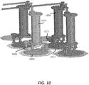
- FIG. 10 illustrates an angled view of vias coupled to inductors configured to provide lateral magnetic fields.
- a package substrate is not shown, although the inductors shown in FIG. 10 may be implemented in a package substrate.
- a first via 1000 is coupled to a first inductor 1002.
- the first inductor 1002 includes several interconnects (e.g., traces, vias, pads) which are configured to operate as a first spiral winding for the first inductor 1002.
- the first inductor 1002 is configured to generate a magnetic field that laterally traverses a substrate.
- the first inductor 1002 is also coupled to a first pad 1004.
- the first pad 1004 may be configured to couple to a solder ball or a landing pad from a landing pad array.
- the first inductor 1002 is positioned such that the magnetic field is directed towards a second inductor 1012.
- the second inductor 1012 is coupled to a second via 1010.
- the second inductor 1012 includes several interconnects (e.g., traces, vias, pads) which are configured to operate as a second spiral winding for the second inductor 1012.
- the second inductor 1012 is configured to generate a magnetic field that laterally traverses a substrate.
- the second inductor 1012 is also coupled to a second pad 1014.
- the second pad 1014 may be configured to couple to a solder ball or a landing pad from a landing pad array.
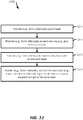
- providing a package substrate that includes an inductor includes several processes.
- FIGS. 11A-11D illustrate an exemplary sequence for providing a package substrate.
- the sequence of FIGS. 11A-11D may be used to provide / manufacture the package substrate of FIGS. 2 and/or 6, and/or other package substrate described in the present disclose.
- FIGS. 11A-11D may combine one or more stages in order to simplify and/or clarify the sequence for providing a package substrate that includes an inductor.
- a core layer 1100 is provided.
- providing the core layer 1100 may include receiving a core layer from a supplier or fabricating a core layer. Different implementations may use different materials for the core layer.
- a first cavity 1101 and a second cavity 1103 are formed in the core layer 1100.
- Different implementations may use different processes for forming the cavities.
- a laser process and/or chemical process e.g., photo etching may be use to remove part of the core layer 1100 to form the cavities.
- a first via 1102 and a second via 1104 are provided (e.g., formed) in the core layer 1100. Specifically a metal layer is provided in the first cavity 1101 to form the first via 1102, and a metal layer is provided in the second cavity 1103 to form the second via 1104. Different implementations may provide the metal layer differently. In some implementations, a plating process is used to provide the metal layer in the cavities. In some implementations, the first via 1102 and/or the second via 1104 is a pin.
- a first metal layer 1110 is provided on a first surface (e.g., top surface) of the core layer 1100.
- the first metal layer 1110 includes a first pad 1110a and a second pad 1110b.
- the first pad 1110a is coupled to a first portion (e.g., top portion) of the first via 1102.
- the second pad 1110b is coupled to a first portion (e.g., top portion) of the second via 1104.
- a second metal layer 1112 is provided on a second surface (e.g., bottom surface) of the core layer 1100.
- the second metal layer 1112 includes a third pad 1112a and a fourth pad 1112b.
- the third pad 1112a is coupled to a second portion (e.g., bottom portion) of the first via 1102.
- the fourth pad 1112b is coupled to a second portion (e.g., bottom portion) of the second via 1104.
- a plating process is used to provide the first metal layer 1110 and the second metal layer 1112.
- a first dielectric layer 1120 is provided on the first surface (e.g., top surface) of the core layer 1100.
- a cavity 1121 and a cavity 1123 are also provided (e.g., formed) in the first dielectric layer 1120.
- a second dielectric layer 1124 is provided on the second surface (e.g., bottom surface) of the core layer 1100.
- a cavity 1125 and a cavity 1127 are also provided (e.g., formed) in the second dielectric layer 1122.
- a first metal layer 1130 is provided on the first dielectric layer 1120.
- the first metal layer 1130 includes a first trace 1130a, a second trace 1130b, a first via 1130c, and a second via 1130d.
- the first via 1130c is formed in the cavity 1121, and the second via 1130d is formed in the cavity 1123.
- a second metal layer 1132 is provided on the second dielectric layer 1122.
- the second metal layer 1132 includes a first trace 1132a, a second trace 1132b, a first via 1132c, and a second via 1132d
- the first via 1132s is formed in the cavity 1125, and the second via 1132d is formed in the cavity 1127.
- a plating process is used to provide the first metal layer 1130 and the second metal layer 1132.
- a dielectric layer 1134 is provided on the first dielectric layer 1120 and the first metal layer 1110.
- a dielectric layer 1136 is provided on the second dielectric layer 1122 and the second metal layer 1112.
- a cavity 1137 and a cavity 1139 are also provided (e.g., formed) in the dielectric layer 1136.
- a first metal layer 1140 is provided on the dielectric layer 1134.
- a second metal layer 1142 is provided on the dielectric layer 1136.
- the second metal layer 1142 includes a first trace 1142a, a second trace 1142b, a first via 1142c, and a second via 1142d.
- the first via 1142s is formed in the cavity 1137, and the second via 1142d is formed in the cavity 1139.
- a plating process is used to provide the first metal layer 1140 and the second metal layer 1142.
- a dielectric layer 1144 is provided on the dielectric layer 1134 and the first metal layer 1140.
- a dielectric layer 1146 is provided on the dielectric layer 1136 and the second metal layer 1142.
- a cavity 1147 and a cavity 1149 are also provided (e.g., formed) in the dielectric layer 1136.
- a first metal layer 1150 is provided on the dielectric layer 1144.
- a second metal layer 1152 is provided on the dielectric layer 1146.
- the second metal layer 1152 includes a first trace 1152a, a second trace 1152b, a first via 1152c, and a second via 1152d.
- the first via 1152s is formed in the cavity 1147, and the second via 1152d is formed in the cavity 1149.
- a plating process is used to provide the first metal layer 1150 and the second metal layer 1152.
- a dielectric layer 1154 is provided on the dielectric layer 1144 and the first metal layer 1150.
- a dielectric layer 1156 is provided on the dielectric layer 1146 and the second metal layer 1152.
- a cavity 1157 and a cavity 1159 are also provided (e.g., formed) in the dielectric layer 1136.
- a first metal layer 1160 is provided on the dielectric layer 1154.
- a second metal layer 1162 is provided on the dielectric layer 1156.
- the second metal layer 1162 includes a first pad 1162a, a second pad 1162b, a first via 1162c, and a second via 1162d.
- the first via 1162c is formed in the cavity 1157, and the second via 1162d is formed in the cavity 1159.
- a plating process is used to provide the first metal layer 1160 and the second metal layer 1162.
- a dielectric layer 1170 is provided on the dielectric layer 1156 and the second metal layer 1162.
- Stage 12 illustrates a first inductor 1180 in the dielectric layers of the package substrate.
- Stage 12 also illustrates a second inductor 1182 in the dielectric layers of the package substrate.
- the first inductor 1180 and the second inductor 1182 are the inductors 222 and 232 of FIG. 2 , inductor 310 of FIG. 3 , inductors 622 and 632 of FIG. 6 , and/or inductor 710 of FIG. 7 .
- providing a package substrate that includes an inductor includes several processes.
- FIG. 12 illustrates an exemplary method for providing a package substrate. In some implementations, the method of FIG. 12 may be used to provide / manufacture the package substrate of FIGS. 2 and/or 6, and/or other package substrate described in the present disclose.
- sequence of FIG. 12 may combine one or more stages in order to simplify and/or clarify the sequence for providing a package substrate that includes an inductor.
- the method provides (at 1205) a core layer.
- providing the core layer 1100 may include receiving a core layer from a supplier or fabricating (e.g., forming) a core layer. Different implementations may use different materials for the core layer.
- Stage 1 of FIG. 11A illustrates an example of providing a core layer
- the method provides (at 1210) at least one via in the core layer.
- providing (e.g., forming) at least one via includes forming a cavity in the core layer and filling the cavity with a metal layer to define a via.
- a plating process is used to provide the via in the core layer.
- Stages 2 and 3 of FIG. 11A illustrates an example of providing at least one via in the core layer. As shown stage 2, a first cavity 1101 and a second cavity 1103 are formed in the core layer 1100. Different implementations may use different processes for forming the cavities. In some implementations, a laser process and/or chemical process (e.g., photo etching) may be use to remove part of the core layer 1100 to form the cavities.
- a first via 1102 and a second via 1104 are provided (e.g., formed) in the core layer 1100.
- a metal layer is provided (e.g., formed) in the first cavity 1101 to form the first via 1102, and a metal layer is provided in the second cavity 1103 to form the second via 1104.
- a plating process is used to provide the metal layer in the cavities.
- a first dielectric layer 1120 is provided on the first surface (e.g., top surface) of the core layer 1100.
- a cavity 1121 and a cavity 1123 are also provided (e.g., formed) in the first dielectric layer 1120.
- a second dielectric layer 1124 is provided on the second surface (e.g., bottom surface) of the core layer 1100.
- a cavity 1125 and a cavity 1127 are also provided (e.g., formed) in the second dielectric layer 1122.
- the method also provides (at 1220) several interconnects in the dielectric layers to define an inductor that is coupled to a via in the core layer.
- providing (e.g., forming) one or more interconnects includes using a plating process to form metal layers in the dielectric layers.
- the interconnects that define the inductor may include traces, vias and/or pads. Stages 3-12 illustrate examples of providing interconnects in the dielectric layers to define an inductor.
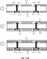
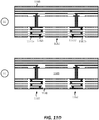
- FIG. 13 conceptually illustrates an example of a package substrate that includes an inductor that is offset from a via (e.g., pin). Specifically, FIG. 13 illustrates a package substrate 1300 that includes a core layer 1302, a first dielectric layer 1304, and a second dielectric layer 1306.
- the first dielectric layer 1304 may include several dielectric layers.
- the second dielectric layer 1306 may include several dielectric layers.
- the core layer 1302 includes a first via 1320 and a second via 1330.
- the first via 1320 and/or the second via 1330 may be a pin.
- the first dielectric layer 1304 includes a first set of interconnects 1314, a first inductor 1322, a first pad 1324, a second inductor 1332, and a second pad 1334.
- the second dielectric layer 1306 includes a second set of interconnects 1316, a third set of interconnects 1326, and a fourth set of interconnects 1336. As shown in FIG. 13 , the second inductor 1332 is offset (e.g., vertically offset) from the second via 1330.
- the first inductor 1322 includes several interconnects (e.g., traces, vias, pads), which are configured to provide a set of windings for the first inductor 1322.
- a first portion (e.g., top portion) of the first inductor 1322 is coupled to a first portion (e.g., bottom portion) of the first via 1320.
- a second portion (e.g., bottom portion) of the first inductor 1322 is coupled to the first pad 1324.
- the first pad 1324 is configured to couple to a set of solder balls.
- a signal interconnect may include one of at least a via (e.g., first via 1320) in the core layer 1302 and/or a set of interconnects (e.g., fourth set of interconnects 1336) in the second dielectric layer 1306.
- the signal interconnect may include the inductor 1322 and/or the inductor 1332.
- an interconnect may include a trace.
- matching the impedance or reducing the difference between the impedance of a signal interconnect and the pad(s) provides better signal performance.
- matching the impedance or reducing the impedance difference reduces signal loss and/or signal degradation between the pad and signal interconnect, thereby providing better signal performance for the package substrate.
- a second portion (e.g., top portion) of the first via 1320 is coupled to the third set of interconnects 1326.
- the third set of interconnects 1326 are located in the second dielectric layer 1306.
- the third set of interconnects 1326 may include traces and/or vias.
- the second inductor 1332 includes several interconnects (e.g., traces, vias, pads), which are configured to provide a set of windings for the second inductor 1332.
- a first portion (e.g., top portion) of the second inductor 1332 is coupled to a first portion (e.g., bottom portion) of the second via 1330.
- a second portion (e.g., bottom portion) of the second inductor 1332 is coupled to the second pad 1334.
- the second pad 1334 is configured to couple to a set of solder balls.
- the second inductor 1332 is configured in such a way that the impedance of the second pad 1334 matches or closely matches the impedance of the signal interconnect to which the second pad 1334 will be coupled to.
- a second portion (e.g., top portion) of the second via 1330 is coupled to the fourth set of interconnects 1336.
- the fourth set of interconnects 1336 are located in the second dielectric layer 1306.
- the fourth set of interconnects 1336 may includes traces and/or vias.
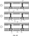
- FIG. 14 conceptually illustrates an example of a package substrate that includes an inductor that can produce a lateral magnetic field, where the inductor is offset form a via (e.g., pin).
- FIG. 14 illustrates a package substrate 1400 that includes a core layer 1402, a first dielectric layer 1404, and a second dielectric layer 1406.
- the first dielectric layer 1404 may include several dielectric layers.
- the second dielectric layer 1406 may include several dielectric layers.
- the core layer 1402 includes a first via 1420 and a second via 1430.
- the first via 1420 and/or the second via 1430 may be a pin.
- the first dielectric layer 1404 includes a first set of interconnects 1414, a first inductor 1422, a first pad 1424, a second inductor 1432, and a second pad 1434.
- the second dielectric layer 1406 includes a second set of interconnects 1416, a third set of interconnects 1426, and a fourth set of interconnects 1436. As shown in FIG. 14 , the second inductor 1432 is offset (e.g., vertically offset) from the second via 1430.
- the first inductor 1422 includes several interconnects (e.g., traces, vias, pads), which are configured to provide a set of windings for the first inductor 1422.
- a first portion (e.g., top portion) of the first inductor 1422 is coupled to a first portion (e.g., bottom portion) of the first via 1420.
- a second portion (e.g., bottom portion) of the first inductor 1422 is coupled to the first pad 1424.
- the first pad 1424 is configured to couple to a set of solder balls.
- the first inductor 1422 is configured in such a way that the impedance of the first pad 1424 matches or closely matches the impedance of the signal interconnect to which the first pad 1424 will be coupled to.
- a signal interconnect may include one of at least a via (e.g., first via 1420) in the core layer 1402 and/or a set of interconnects (e.g., fourth set of interconnects 1436) in the second dielectric layer 1406.
- the signal interconnect may include the inductor 1422 and/or the inductor 1432.
- an interconnect may include a trace.
- the first inductor 1422 may be configured to provide a magnetic field that laterally traverses the package substrate 1400.
- matching the impedance or reducing the difference between the impedance of the signal interconnect and the pads provides better signal performance.
- matching the impedance or reducing the impedance difference reduces signal loss and/or signal degradation between the pad and the signal interconnect, thereby providing better signal performance for the package substrate.
- a second portion (e.g., top portion) of the first via 1420 is coupled to the third set of interconnects 1426.
- the third set of interconnects 1426 are located in the second dielectric layer 1406.
- the third set of interconnects 1426 may includes traces and/or vias.
- the second inductor 1432 includes several interconnects (e.g., traces, vias, pads), which are configured to provide a set of windings for the second inductor 1432.
- a first portion (e.g., top portion) of the second inductor 1432 is coupled to a first portion (e.g., bottom portion) of the second via 1430.
- a second portion (e.g., bottom portion) of the second inductor 1432 is coupled to the second pad 1434.
- the second pad 1434 is configured to couple to a set of solder balls.
- the second inductor 1432 is configured in such a way that the impedance of the second pad 1434 matches or closely matches the impedance of the signal interconnect to which the second pad 1434 will be coupled to.
- the second inductor 1432 may be configured to provide a magnetic field that laterally traverses the package substrate 1400.
- a second portion (e.g., top portion) of the second via 1430 is coupled to the fourth set of interconnects 1436.
- the fourth set of interconnects 1436 are located in the second dielectric layer 1406.
- the fourth set of interconnects 1436 may includes traces and/or vias.
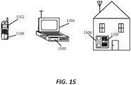
- FIG. 15 illustrates various electronic devices that may be integrated with any of the aforementioned semiconductor device, package substrate, integrated circuit, die, interposer or package.
- a mobile telephone 1502, a laptop computer 1504, and a fixed location terminal 1506 may include an integrated circuit (IC) 1500 as described herein.
- the IC 1500 may be, for example, any of the integrated circuits, dice or packages described herein.
- the devices 1502, 1504, 1506 illustrated in FIG. 15 are merely exemplary.
- IC 1500 may also feature the IC 1500 including, but not limited to, mobile devices, hand-held personal communication systems (PCS) units, portable data units such as personal digital assistants, GPS enabled devices, navigation devices, set top boxes, music players, video players, entertainment units, fixed location data units such as meter reading equipment, communications devices, smartphones, tablet computers or any other device that stores or retrieves data or computer instructions, or any combination thereof.
- PCS personal communication systems
- FIGS. 2, 3 , 4 , 5 , 6, 7 , 8, 9 , 10 , 11A-11D , 12 , 13, 14 and/or 15 and its corresponding description in the present disclosure is not limited to dies and/or ICs.
- FIGS. 2, 3 , 4 , 5 , 6, 7 , 8, 9 , 10 , 11A-11D , 12 , 13, 14 and/or 15 and its corresponding description may be used to manufacture, create, provide, and/or produce integrated devices.
- an integrated device may include a die package, package substrate, an integrated circuit (IC), a wafer, a semiconductor device, and/or an interposer.
- IC integrated circuit
- Coupled is used herein to refer to the direct or indirect coupling between two objects. For example, if object A physically touches object B, and object B touches object C, then objects A and C may still be considered coupled to one another—even if they do not directly physically touch each other.
- the embodiments may be described as a process that is depicted as a flowchart, a flow diagram, a structure diagram, or a block diagram. Although a flowchart may describe the operations as a sequential process, many of the operations can be performed in parallel or concurrently. In addition, the order of the operations may be re-arranged. A process is terminated when its operations are completed.
Landscapes
- Engineering & Computer Science (AREA)
- Power Engineering (AREA)
- Microelectronics & Electronic Packaging (AREA)
- Physics & Mathematics (AREA)
- Condensed Matter Physics & Semiconductors (AREA)
- General Physics & Mathematics (AREA)
- Computer Hardware Design (AREA)
- Production Of Multi-Layered Print Wiring Board (AREA)
- Coils Or Transformers For Communication (AREA)
- Parts Printed On Printed Circuit Boards (AREA)
Applications Claiming Priority (2)
| Application Number | Priority Date | Filing Date | Title |
|---|---|---|---|
| US14/229,367 US10008316B2 (en) | 2014-03-28 | 2014-03-28 | Inductor embedded in a package substrate |
| PCT/US2015/023129 WO2015148996A1 (en) | 2014-03-28 | 2015-03-27 | Inductor embedded in a package subtrate |
Publications (2)
| Publication Number | Publication Date |
|---|---|
| EP3123508A1 EP3123508A1 (en) | 2017-02-01 |
| EP3123508B1 true EP3123508B1 (en) | 2021-09-29 |
Family
ID=52815380
Family Applications (1)
| Application Number | Title | Priority Date | Filing Date |
|---|---|---|---|
| EP15715112.7A Active EP3123508B1 (en) | 2014-03-28 | 2015-03-27 | Inductor embedded in a package subtrate |
Country Status (7)
Families Citing this family (13)
| Publication number | Priority date | Publication date | Assignee | Title |
|---|---|---|---|---|
| US9496213B2 (en) * | 2015-02-05 | 2016-11-15 | Qualcomm Incorporated | Integrated device package comprising a magnetic core inductor with protective ring embedded in a package substrate |
| CN107408534B (zh) | 2015-02-11 | 2019-11-29 | 朝阳半导体技术江阴有限公司 | 具有集成无源组件的开关式功率级 |
| KR101933408B1 (ko) * | 2015-11-10 | 2018-12-28 | 삼성전기 주식회사 | 전자부품 패키지 및 이를 포함하는 전자기기 |
| CN108293294A (zh) * | 2015-12-31 | 2018-07-17 | 英特尔公司 | 用于封装和pcb中针对具有盲孔和埋孔的组装件的电感补偿的微线圈装置 |
| US9859357B1 (en) * | 2016-07-14 | 2018-01-02 | International Business Machines Corporation | Magnetic inductor stacks with multilayer isolation layers |
| US10283249B2 (en) | 2016-09-30 | 2019-05-07 | International Business Machines Corporation | Method for fabricating a magnetic material stack |
| US10923417B2 (en) * | 2017-04-26 | 2021-02-16 | Taiwan Semiconductor Manufacturing Company Limited | Integrated fan-out package with 3D magnetic core inductor |
| US11158448B2 (en) | 2018-06-14 | 2021-10-26 | Taiwan Semiconductor Manufacturing Company, Ltd. | Packaging layer inductor |
| KR102678311B1 (ko) * | 2018-08-30 | 2024-06-25 | 삼성전자주식회사 | 패키지 볼을 갖는 반도체 패키지를 포함하는 전자 소자 |
| US11640968B2 (en) * | 2018-11-06 | 2023-05-02 | Texas Instruments Incorporated | Inductor on microelectronic die |
| CN113284880A (zh) * | 2021-04-01 | 2021-08-20 | 日月光半导体制造股份有限公司 | 基板内连线结构 |
| CN117059600A (zh) * | 2022-05-06 | 2023-11-14 | 华为技术有限公司 | 基板、封装结构及电子设备 |
| US20250246357A1 (en) * | 2024-01-31 | 2025-07-31 | Avago Technologies International Sales Pte. Limited | Systems and methods for integrating inductors within printed circuit boards |
Family Cites Families (25)
| Publication number | Priority date | Publication date | Assignee | Title |
|---|---|---|---|---|
| US4757295A (en) * | 1987-09-16 | 1988-07-12 | Avco Research Laboratory, Inc. | Transmission line pulsed transformer |
| JPH06151185A (ja) * | 1992-11-09 | 1994-05-31 | Matsushita Electric Works Ltd | 平面型インダクタンス素子 |
| US6177732B1 (en) | 1999-05-27 | 2001-01-23 | Intel Corporation | Multi-layer organic land grid array to minimize via inductance |
| JP2002100733A (ja) * | 2000-09-21 | 2002-04-05 | Nec Corp | 高周波集積回路装置 |
| US7253497B2 (en) | 2003-07-02 | 2007-08-07 | Lsi Corporation | Integrated circuit with inductor having horizontal magnetic flux lines |
| TWI245592B (en) | 2004-01-12 | 2005-12-11 | Advanced Semiconductor Eng | Circuit substrate |
| US7196607B2 (en) | 2004-03-26 | 2007-03-27 | Harris Corporation | Embedded toroidal transformers in ceramic substrates |
| US7227247B2 (en) * | 2005-02-16 | 2007-06-05 | Intel Corporation | IC package with signal land pads |
| US20060220773A1 (en) * | 2005-03-31 | 2006-10-05 | Jun Su | Spiral transformers and associated methods of operation |
| US7474539B2 (en) * | 2005-04-11 | 2009-01-06 | Intel Corporation | Inductor |
| US7907043B2 (en) * | 2005-11-30 | 2011-03-15 | Ryutaro Mori | Planar inductor |
| US7843302B2 (en) * | 2006-05-08 | 2010-11-30 | Ibiden Co., Ltd. | Inductor and electric power supply using it |
| US7649265B2 (en) | 2006-09-29 | 2010-01-19 | Intel Corporation | Micro-via structure design for high performance integrated circuits |
| US8222714B2 (en) | 2007-02-05 | 2012-07-17 | Rambus Inc. | Semiconductor package with embedded spiral inductor |
| TWI347616B (en) * | 2007-03-22 | 2011-08-21 | Ind Tech Res Inst | Inductor devices |
| JP2008277485A (ja) * | 2007-04-27 | 2008-11-13 | Fuji Electric Device Technology Co Ltd | トランスユニットおよび電力変換装置 |
| US7733207B2 (en) * | 2007-05-31 | 2010-06-08 | Electronics And Telecommunications Research Institute | Vertically formed inductor and electronic device having the same |
| JP2009055019A (ja) * | 2007-07-30 | 2009-03-12 | Renesas Technology Corp | 多層基板、半導体集積回路用パッケージ基板及び半導体集積回路実装用プリント配線板 |
| US20090085155A1 (en) | 2007-09-28 | 2009-04-02 | Bailey Mark J | Method and apparatus for package-to-board impedance matching for high speed integrated circuits |
| WO2010035401A1 (ja) | 2008-09-26 | 2010-04-01 | パナソニック株式会社 | 電子デバイス及びその製造方法 |
| US8067816B2 (en) | 2009-02-03 | 2011-11-29 | Qualcomm Incorporated | Techniques for placement of active and passive devices within a chip |
| US8384507B2 (en) | 2010-06-01 | 2013-02-26 | Qualcomm Incorporated | Through via inductor or transformer in a high-resistance substrate with programmability |
| US9048112B2 (en) * | 2010-06-29 | 2015-06-02 | Qualcomm Incorporated | Integrated voltage regulator with embedded passive device(s) for a stacked IC |
| US8723048B2 (en) * | 2010-11-09 | 2014-05-13 | Broadcom Corporation | Three-dimensional coiling via structure for impedance tuning of impedance discontinuity |
| US8405482B2 (en) * | 2011-02-23 | 2013-03-26 | Taiwan Semiconductor Manufacturing Company, Ltd. | Integrated circuits including inductors |
-
2014
- 2014-03-28 US US14/229,367 patent/US10008316B2/en active Active
-
2015
- 2015-03-27 EP EP15715112.7A patent/EP3123508B1/en active Active
- 2015-03-27 JP JP2016558646A patent/JP6502378B2/ja active Active
- 2015-03-27 KR KR1020167026201A patent/KR101971195B1/ko active Active
- 2015-03-27 CN CN201580016458.9A patent/CN106133904B/zh not_active Expired - Fee Related
- 2015-03-27 ES ES15715112T patent/ES2895077T3/es active Active
- 2015-03-27 WO PCT/US2015/023129 patent/WO2015148996A1/en active Application Filing
Also Published As
| Publication number | Publication date |
|---|---|
| KR101971195B1 (ko) | 2019-08-13 |
| EP3123508A1 (en) | 2017-02-01 |
| JP6502378B2 (ja) | 2019-04-17 |
| US10008316B2 (en) | 2018-06-26 |
| JP2017511602A (ja) | 2017-04-20 |
| CN106133904B (zh) | 2020-01-10 |
| CN106133904A (zh) | 2016-11-16 |
| KR20160138411A (ko) | 2016-12-05 |
| WO2015148996A1 (en) | 2015-10-01 |
| US20150279545A1 (en) | 2015-10-01 |
| ES2895077T3 (es) | 2022-02-17 |
Similar Documents
| Publication | Publication Date | Title |
|---|---|---|
| EP3123508B1 (en) | Inductor embedded in a package subtrate | |
| US9642259B2 (en) | Embedded bridge structure in a substrate | |
| US9633977B1 (en) | Integrated device comprising flexible connector between integrated circuit (IC) packages | |
| US9209131B2 (en) | Toroid inductor in redistribution layers (RDL) of an integrated device | |
| US9159670B2 (en) | Ultra fine pitch and spacing interconnects for substrate | |
| US9165791B2 (en) | Wireless interconnects in an interposer | |
| US8772951B1 (en) | Ultra fine pitch and spacing interconnects for substrate | |
| US9425143B2 (en) | Integrated device package comprising an electromagnetic (EM) passive device in an encapsulation layer, and an EM shield | |
| US9490226B2 (en) | Integrated device comprising a heat-dissipation layer providing an electrical path for a ground signal | |
| JP2017520929A (ja) | 同軸配線を備える集積デバイス | |
| US9355898B2 (en) | Package on package (PoP) integrated device comprising a plurality of solder resist layers | |
| US20160056226A1 (en) | Wafer level package (wlp) integrated device comprising electromagnetic (em) passive device in redistribution portion, and radio frequency (rf) shield | |
| US9530739B2 (en) | Package on package (PoP) device comprising a high performance inter package connection | |
| CN107567656B (zh) | 包括管芯到线缆连接器的管芯封装以及被配置成耦合至管芯封装的线缆到管芯连接器 | |
| US9324779B2 (en) | Toroid inductor in an integrated device | |
| US10157824B2 (en) | Integrated circuit (IC) package and package substrate comprising stacked vias | |
| KR20180111840A (ko) | 집적 회로(ic) 패키지들 사이의 플렉시블 커넥터를 포함하는 통합 디바이스 | |
| US10170232B2 (en) | Toroid inductor with reduced electromagnetic field leakage | |
| US11955409B2 (en) | Substrate comprising interconnects in a core layer configured for skew matching |
Legal Events
| Date | Code | Title | Description |
|---|---|---|---|
| STAA | Information on the status of an ep patent application or granted ep patent |
Free format text: STATUS: THE INTERNATIONAL PUBLICATION HAS BEEN MADE |
|
| PUAI | Public reference made under article 153(3) epc to a published international application that has entered the european phase |
Free format text: ORIGINAL CODE: 0009012 |
|
| STAA | Information on the status of an ep patent application or granted ep patent |
Free format text: STATUS: REQUEST FOR EXAMINATION WAS MADE |
|
| 17P | Request for examination filed |
Effective date: 20161024 |
|
| AK | Designated contracting states |
Kind code of ref document: A1 Designated state(s): AL AT BE BG CH CY CZ DE DK EE ES FI FR GB GR HR HU IE IS IT LI LT LU LV MC MK MT NL NO PL PT RO RS SE SI SK SM TR |
|
| AX | Request for extension of the european patent |
Extension state: BA ME |
|
| DAV | Request for validation of the european patent (deleted) | ||
| DAX | Request for extension of the european patent (deleted) | ||
| STAA | Information on the status of an ep patent application or granted ep patent |
Free format text: STATUS: EXAMINATION IS IN PROGRESS |
|
| 17Q | First examination report despatched |
Effective date: 20190826 |
|
| GRAP | Despatch of communication of intention to grant a patent |
Free format text: ORIGINAL CODE: EPIDOSNIGR1 |
|
| STAA | Information on the status of an ep patent application or granted ep patent |
Free format text: STATUS: GRANT OF PATENT IS INTENDED |
|
| INTG | Intention to grant announced |
Effective date: 20210419 |
|
| GRAS | Grant fee paid |
Free format text: ORIGINAL CODE: EPIDOSNIGR3 |
|
| GRAA | (expected) grant |
Free format text: ORIGINAL CODE: 0009210 |
|
| STAA | Information on the status of an ep patent application or granted ep patent |
Free format text: STATUS: THE PATENT HAS BEEN GRANTED |
|
| AK | Designated contracting states |
Kind code of ref document: B1 Designated state(s): AL AT BE BG CH CY CZ DE DK EE ES FI FR GB GR HR HU IE IS IT LI LT LU LV MC MK MT NL NO PL PT RO RS SE SI SK SM TR |
|
| REG | Reference to a national code |
Ref country code: GB Ref legal event code: FG4D |
|
| REG | Reference to a national code |
Ref country code: CH Ref legal event code: EP Ref country code: AT Ref legal event code: REF Ref document number: 1434960 Country of ref document: AT Kind code of ref document: T Effective date: 20211015 |
|
| REG | Reference to a national code |
Ref country code: DE Ref legal event code: R096 Ref document number: 602015073676 Country of ref document: DE |
|
| REG | Reference to a national code |
Ref country code: IE Ref legal event code: FG4D |
|
| REG | Reference to a national code |
Ref country code: SE Ref legal event code: TRGR |
|
| REG | Reference to a national code |
Ref country code: NL Ref legal event code: FP |
|
| REG | Reference to a national code |
Ref country code: LT Ref legal event code: MG9D |
|
| PG25 | Lapsed in a contracting state [announced via postgrant information from national office to epo] |
Ref country code: FI Free format text: LAPSE BECAUSE OF FAILURE TO SUBMIT A TRANSLATION OF THE DESCRIPTION OR TO PAY THE FEE WITHIN THE PRESCRIBED TIME-LIMIT Effective date: 20210929 Ref country code: NO Free format text: LAPSE BECAUSE OF FAILURE TO SUBMIT A TRANSLATION OF THE DESCRIPTION OR TO PAY THE FEE WITHIN THE PRESCRIBED TIME-LIMIT Effective date: 20211229 Ref country code: LT Free format text: LAPSE BECAUSE OF FAILURE TO SUBMIT A TRANSLATION OF THE DESCRIPTION OR TO PAY THE FEE WITHIN THE PRESCRIBED TIME-LIMIT Effective date: 20210929 Ref country code: BG Free format text: LAPSE BECAUSE OF FAILURE TO SUBMIT A TRANSLATION OF THE DESCRIPTION OR TO PAY THE FEE WITHIN THE PRESCRIBED TIME-LIMIT Effective date: 20211229 Ref country code: RS Free format text: LAPSE BECAUSE OF FAILURE TO SUBMIT A TRANSLATION OF THE DESCRIPTION OR TO PAY THE FEE WITHIN THE PRESCRIBED TIME-LIMIT Effective date: 20210929 Ref country code: HR Free format text: LAPSE BECAUSE OF FAILURE TO SUBMIT A TRANSLATION OF THE DESCRIPTION OR TO PAY THE FEE WITHIN THE PRESCRIBED TIME-LIMIT Effective date: 20210929 |
|
| REG | Reference to a national code |
Ref country code: AT Ref legal event code: MK05 Ref document number: 1434960 Country of ref document: AT Kind code of ref document: T Effective date: 20210929 |
|
| REG | Reference to a national code |
Ref country code: ES Ref legal event code: FG2A Ref document number: 2895077 Country of ref document: ES Kind code of ref document: T3 Effective date: 20220217 |
|
| PG25 | Lapsed in a contracting state [announced via postgrant information from national office to epo] |
Ref country code: LV Free format text: LAPSE BECAUSE OF FAILURE TO SUBMIT A TRANSLATION OF THE DESCRIPTION OR TO PAY THE FEE WITHIN THE PRESCRIBED TIME-LIMIT Effective date: 20210929 Ref country code: GR Free format text: LAPSE BECAUSE OF FAILURE TO SUBMIT A TRANSLATION OF THE DESCRIPTION OR TO PAY THE FEE WITHIN THE PRESCRIBED TIME-LIMIT Effective date: 20211230 |
|
| PG25 | Lapsed in a contracting state [announced via postgrant information from national office to epo] |
Ref country code: AT Free format text: LAPSE BECAUSE OF FAILURE TO SUBMIT A TRANSLATION OF THE DESCRIPTION OR TO PAY THE FEE WITHIN THE PRESCRIBED TIME-LIMIT Effective date: 20210929 |
|
| PG25 | Lapsed in a contracting state [announced via postgrant information from national office to epo] |
Ref country code: IS Free format text: LAPSE BECAUSE OF FAILURE TO SUBMIT A TRANSLATION OF THE DESCRIPTION OR TO PAY THE FEE WITHIN THE PRESCRIBED TIME-LIMIT Effective date: 20220129 Ref country code: SK Free format text: LAPSE BECAUSE OF FAILURE TO SUBMIT A TRANSLATION OF THE DESCRIPTION OR TO PAY THE FEE WITHIN THE PRESCRIBED TIME-LIMIT Effective date: 20210929 Ref country code: RO Free format text: LAPSE BECAUSE OF FAILURE TO SUBMIT A TRANSLATION OF THE DESCRIPTION OR TO PAY THE FEE WITHIN THE PRESCRIBED TIME-LIMIT Effective date: 20210929 Ref country code: PT Free format text: LAPSE BECAUSE OF FAILURE TO SUBMIT A TRANSLATION OF THE DESCRIPTION OR TO PAY THE FEE WITHIN THE PRESCRIBED TIME-LIMIT Effective date: 20220131 Ref country code: PL Free format text: LAPSE BECAUSE OF FAILURE TO SUBMIT A TRANSLATION OF THE DESCRIPTION OR TO PAY THE FEE WITHIN THE PRESCRIBED TIME-LIMIT Effective date: 20210929 Ref country code: EE Free format text: LAPSE BECAUSE OF FAILURE TO SUBMIT A TRANSLATION OF THE DESCRIPTION OR TO PAY THE FEE WITHIN THE PRESCRIBED TIME-LIMIT Effective date: 20210929 Ref country code: CZ Free format text: LAPSE BECAUSE OF FAILURE TO SUBMIT A TRANSLATION OF THE DESCRIPTION OR TO PAY THE FEE WITHIN THE PRESCRIBED TIME-LIMIT Effective date: 20210929 Ref country code: AL Free format text: LAPSE BECAUSE OF FAILURE TO SUBMIT A TRANSLATION OF THE DESCRIPTION OR TO PAY THE FEE WITHIN THE PRESCRIBED TIME-LIMIT Effective date: 20210929 |
|
| REG | Reference to a national code |
Ref country code: DE Ref legal event code: R097 Ref document number: 602015073676 Country of ref document: DE |
|
| PG25 | Lapsed in a contracting state [announced via postgrant information from national office to epo] |
Ref country code: DK Free format text: LAPSE BECAUSE OF FAILURE TO SUBMIT A TRANSLATION OF THE DESCRIPTION OR TO PAY THE FEE WITHIN THE PRESCRIBED TIME-LIMIT Effective date: 20210929 |
|
| PLBE | No opposition filed within time limit |
Free format text: ORIGINAL CODE: 0009261 |
|
| STAA | Information on the status of an ep patent application or granted ep patent |
Free format text: STATUS: NO OPPOSITION FILED WITHIN TIME LIMIT |
|
| 26N | No opposition filed |
Effective date: 20220630 |
|
| PG25 | Lapsed in a contracting state [announced via postgrant information from national office to epo] |
Ref country code: MC Free format text: LAPSE BECAUSE OF FAILURE TO SUBMIT A TRANSLATION OF THE DESCRIPTION OR TO PAY THE FEE WITHIN THE PRESCRIBED TIME-LIMIT Effective date: 20210929 |
|
| PG25 | Lapsed in a contracting state [announced via postgrant information from national office to epo] |
Ref country code: SI Free format text: LAPSE BECAUSE OF FAILURE TO SUBMIT A TRANSLATION OF THE DESCRIPTION OR TO PAY THE FEE WITHIN THE PRESCRIBED TIME-LIMIT Effective date: 20210929 |
|
| REG | Reference to a national code |
Ref country code: BE Ref legal event code: MM Effective date: 20220331 |
|
| PG25 | Lapsed in a contracting state [announced via postgrant information from national office to epo] |
Ref country code: LU Free format text: LAPSE BECAUSE OF NON-PAYMENT OF DUE FEES Effective date: 20220327 Ref country code: IE Free format text: LAPSE BECAUSE OF NON-PAYMENT OF DUE FEES Effective date: 20220327 |
|
| PG25 | Lapsed in a contracting state [announced via postgrant information from national office to epo] |
Ref country code: BE Free format text: LAPSE BECAUSE OF NON-PAYMENT OF DUE FEES Effective date: 20220331 |
|
| PG25 | Lapsed in a contracting state [announced via postgrant information from national office to epo] |
Ref country code: HU Free format text: LAPSE BECAUSE OF FAILURE TO SUBMIT A TRANSLATION OF THE DESCRIPTION OR TO PAY THE FEE WITHIN THE PRESCRIBED TIME-LIMIT; INVALID AB INITIO Effective date: 20150327 |
|
| PG25 | Lapsed in a contracting state [announced via postgrant information from national office to epo] |
Ref country code: SM Free format text: LAPSE BECAUSE OF FAILURE TO SUBMIT A TRANSLATION OF THE DESCRIPTION OR TO PAY THE FEE WITHIN THE PRESCRIBED TIME-LIMIT Effective date: 20210929 Ref country code: MK Free format text: LAPSE BECAUSE OF FAILURE TO SUBMIT A TRANSLATION OF THE DESCRIPTION OR TO PAY THE FEE WITHIN THE PRESCRIBED TIME-LIMIT Effective date: 20210929 Ref country code: CY Free format text: LAPSE BECAUSE OF FAILURE TO SUBMIT A TRANSLATION OF THE DESCRIPTION OR TO PAY THE FEE WITHIN THE PRESCRIBED TIME-LIMIT Effective date: 20210929 |
|
| PG25 | Lapsed in a contracting state [announced via postgrant information from national office to epo] |
Ref country code: MT Free format text: LAPSE BECAUSE OF FAILURE TO SUBMIT A TRANSLATION OF THE DESCRIPTION OR TO PAY THE FEE WITHIN THE PRESCRIBED TIME-LIMIT Effective date: 20210929 |
|
| PGFP | Annual fee paid to national office [announced via postgrant information from national office to epo] |
Ref country code: NL Payment date: 20250212 Year of fee payment: 11 |
|
| PGFP | Annual fee paid to national office [announced via postgrant information from national office to epo] |
Ref country code: SE Payment date: 20250310 Year of fee payment: 11 |
|
| PGFP | Annual fee paid to national office [announced via postgrant information from national office to epo] |
Ref country code: DE Payment date: 20250210 Year of fee payment: 11 |
|
| PGFP | Annual fee paid to national office [announced via postgrant information from national office to epo] |
Ref country code: FR Payment date: 20250211 Year of fee payment: 11 |
|
| PGFP | Annual fee paid to national office [announced via postgrant information from national office to epo] |
Ref country code: GB Payment date: 20250213 Year of fee payment: 11 Ref country code: IT Payment date: 20250312 Year of fee payment: 11 |
|
| PGFP | Annual fee paid to national office [announced via postgrant information from national office to epo] |
Ref country code: ES Payment date: 20250409 Year of fee payment: 11 |
|
| PGFP | Annual fee paid to national office [announced via postgrant information from national office to epo] |
Ref country code: CH Payment date: 20250401 Year of fee payment: 11 |