EP3121840A1 - Thin-film transistor and preparation method therefor, array substrate, and display panel - Google Patents
Thin-film transistor and preparation method therefor, array substrate, and display panel Download PDFInfo
- Publication number
- EP3121840A1 EP3121840A1 EP15882903.6A EP15882903A EP3121840A1 EP 3121840 A1 EP3121840 A1 EP 3121840A1 EP 15882903 A EP15882903 A EP 15882903A EP 3121840 A1 EP3121840 A1 EP 3121840A1
- Authority
- EP
- European Patent Office
- Prior art keywords
- layer
- thin film
- metal
- gate electrode
- drain electrode
- Prior art date
- Legal status (The legal status is an assumption and is not a legal conclusion. Google has not performed a legal analysis and makes no representation as to the accuracy of the status listed.)
- Granted
Links
Images


Classifications
-
- B—PERFORMING OPERATIONS; TRANSPORTING
- B82—NANOTECHNOLOGY
- B82Y—SPECIFIC USES OR APPLICATIONS OF NANOSTRUCTURES; MEASUREMENT OR ANALYSIS OF NANOSTRUCTURES; MANUFACTURE OR TREATMENT OF NANOSTRUCTURES
- B82Y30/00—Nanotechnology for materials or surface science, e.g. nanocomposites
-
- C—CHEMISTRY; METALLURGY
- C09—DYES; PAINTS; POLISHES; NATURAL RESINS; ADHESIVES; COMPOSITIONS NOT OTHERWISE PROVIDED FOR; APPLICATIONS OF MATERIALS NOT OTHERWISE PROVIDED FOR
- C09D—COATING COMPOSITIONS, e.g. PAINTS, VARNISHES OR LACQUERS; FILLING PASTES; CHEMICAL PAINT OR INK REMOVERS; INKS; CORRECTING FLUIDS; WOODSTAINS; PASTES OR SOLIDS FOR COLOURING OR PRINTING; USE OF MATERIALS THEREFOR
- C09D11/00—Inks
- C09D11/52—Electrically conductive inks
-
- C—CHEMISTRY; METALLURGY
- C23—COATING METALLIC MATERIAL; COATING MATERIAL WITH METALLIC MATERIAL; CHEMICAL SURFACE TREATMENT; DIFFUSION TREATMENT OF METALLIC MATERIAL; COATING BY VACUUM EVAPORATION, BY SPUTTERING, BY ION IMPLANTATION OR BY CHEMICAL VAPOUR DEPOSITION, IN GENERAL; INHIBITING CORROSION OF METALLIC MATERIAL OR INCRUSTATION IN GENERAL
- C23C—COATING METALLIC MATERIAL; COATING MATERIAL WITH METALLIC MATERIAL; SURFACE TREATMENT OF METALLIC MATERIAL BY DIFFUSION INTO THE SURFACE, BY CHEMICAL CONVERSION OR SUBSTITUTION; COATING BY VACUUM EVAPORATION, BY SPUTTERING, BY ION IMPLANTATION OR BY CHEMICAL VAPOUR DEPOSITION, IN GENERAL
- C23C14/00—Coating by vacuum evaporation, by sputtering or by ion implantation of the coating forming material
- C23C14/58—After-treatment
- C23C14/5806—Thermal treatment
-
- C—CHEMISTRY; METALLURGY
- C23—COATING METALLIC MATERIAL; COATING MATERIAL WITH METALLIC MATERIAL; CHEMICAL SURFACE TREATMENT; DIFFUSION TREATMENT OF METALLIC MATERIAL; COATING BY VACUUM EVAPORATION, BY SPUTTERING, BY ION IMPLANTATION OR BY CHEMICAL VAPOUR DEPOSITION, IN GENERAL; INHIBITING CORROSION OF METALLIC MATERIAL OR INCRUSTATION IN GENERAL
- C23C—COATING METALLIC MATERIAL; COATING MATERIAL WITH METALLIC MATERIAL; SURFACE TREATMENT OF METALLIC MATERIAL BY DIFFUSION INTO THE SURFACE, BY CHEMICAL CONVERSION OR SUBSTITUTION; COATING BY VACUUM EVAPORATION, BY SPUTTERING, BY ION IMPLANTATION OR BY CHEMICAL VAPOUR DEPOSITION, IN GENERAL
- C23C14/00—Coating by vacuum evaporation, by sputtering or by ion implantation of the coating forming material
- C23C14/58—After-treatment
- C23C14/5846—Reactive treatment
- C23C14/5853—Oxidation
-
- C—CHEMISTRY; METALLURGY
- C23—COATING METALLIC MATERIAL; COATING MATERIAL WITH METALLIC MATERIAL; CHEMICAL SURFACE TREATMENT; DIFFUSION TREATMENT OF METALLIC MATERIAL; COATING BY VACUUM EVAPORATION, BY SPUTTERING, BY ION IMPLANTATION OR BY CHEMICAL VAPOUR DEPOSITION, IN GENERAL; INHIBITING CORROSION OF METALLIC MATERIAL OR INCRUSTATION IN GENERAL
- C23C—COATING METALLIC MATERIAL; COATING MATERIAL WITH METALLIC MATERIAL; SURFACE TREATMENT OF METALLIC MATERIAL BY DIFFUSION INTO THE SURFACE, BY CHEMICAL CONVERSION OR SUBSTITUTION; COATING BY VACUUM EVAPORATION, BY SPUTTERING, BY ION IMPLANTATION OR BY CHEMICAL VAPOUR DEPOSITION, IN GENERAL
- C23C14/00—Coating by vacuum evaporation, by sputtering or by ion implantation of the coating forming material
- C23C14/58—After-treatment
- C23C14/5873—Removal of material
-
- C—CHEMISTRY; METALLURGY
- C23—COATING METALLIC MATERIAL; COATING MATERIAL WITH METALLIC MATERIAL; CHEMICAL SURFACE TREATMENT; DIFFUSION TREATMENT OF METALLIC MATERIAL; COATING BY VACUUM EVAPORATION, BY SPUTTERING, BY ION IMPLANTATION OR BY CHEMICAL VAPOUR DEPOSITION, IN GENERAL; INHIBITING CORROSION OF METALLIC MATERIAL OR INCRUSTATION IN GENERAL
- C23C—COATING METALLIC MATERIAL; COATING MATERIAL WITH METALLIC MATERIAL; SURFACE TREATMENT OF METALLIC MATERIAL BY DIFFUSION INTO THE SURFACE, BY CHEMICAL CONVERSION OR SUBSTITUTION; COATING BY VACUUM EVAPORATION, BY SPUTTERING, BY ION IMPLANTATION OR BY CHEMICAL VAPOUR DEPOSITION, IN GENERAL
- C23C16/00—Chemical coating by decomposition of gaseous compounds, without leaving reaction products of surface material in the coating, i.e. chemical vapour deposition [CVD] processes
- C23C16/56—After-treatment
-
- C—CHEMISTRY; METALLURGY
- C23—COATING METALLIC MATERIAL; COATING MATERIAL WITH METALLIC MATERIAL; CHEMICAL SURFACE TREATMENT; DIFFUSION TREATMENT OF METALLIC MATERIAL; COATING BY VACUUM EVAPORATION, BY SPUTTERING, BY ION IMPLANTATION OR BY CHEMICAL VAPOUR DEPOSITION, IN GENERAL; INHIBITING CORROSION OF METALLIC MATERIAL OR INCRUSTATION IN GENERAL
- C23C—COATING METALLIC MATERIAL; COATING MATERIAL WITH METALLIC MATERIAL; SURFACE TREATMENT OF METALLIC MATERIAL BY DIFFUSION INTO THE SURFACE, BY CHEMICAL CONVERSION OR SUBSTITUTION; COATING BY VACUUM EVAPORATION, BY SPUTTERING, BY ION IMPLANTATION OR BY CHEMICAL VAPOUR DEPOSITION, IN GENERAL
- C23C18/00—Chemical coating by decomposition of either liquid compounds or solutions of the coating forming compounds, without leaving reaction products of surface material in the coating; Contact plating
- C23C18/02—Chemical coating by decomposition of either liquid compounds or solutions of the coating forming compounds, without leaving reaction products of surface material in the coating; Contact plating by thermal decomposition
- C23C18/08—Chemical coating by decomposition of either liquid compounds or solutions of the coating forming compounds, without leaving reaction products of surface material in the coating; Contact plating by thermal decomposition characterised by the deposition of metallic material
-
- C—CHEMISTRY; METALLURGY
- C23—COATING METALLIC MATERIAL; COATING MATERIAL WITH METALLIC MATERIAL; CHEMICAL SURFACE TREATMENT; DIFFUSION TREATMENT OF METALLIC MATERIAL; COATING BY VACUUM EVAPORATION, BY SPUTTERING, BY ION IMPLANTATION OR BY CHEMICAL VAPOUR DEPOSITION, IN GENERAL; INHIBITING CORROSION OF METALLIC MATERIAL OR INCRUSTATION IN GENERAL
- C23C—COATING METALLIC MATERIAL; COATING MATERIAL WITH METALLIC MATERIAL; SURFACE TREATMENT OF METALLIC MATERIAL BY DIFFUSION INTO THE SURFACE, BY CHEMICAL CONVERSION OR SUBSTITUTION; COATING BY VACUUM EVAPORATION, BY SPUTTERING, BY ION IMPLANTATION OR BY CHEMICAL VAPOUR DEPOSITION, IN GENERAL
- C23C30/00—Coating with metallic material characterised only by the composition of the metallic material, i.e. not characterised by the coating process
-
- H—ELECTRICITY
- H10—SEMICONDUCTOR DEVICES; ELECTRIC SOLID-STATE DEVICES NOT OTHERWISE PROVIDED FOR
- H10D—INORGANIC ELECTRIC SEMICONDUCTOR DEVICES
- H10D30/00—Field-effect transistors [FET]
- H10D30/60—Insulated-gate field-effect transistors [IGFET]
- H10D30/67—Thin-film transistors [TFT]
- H10D30/6729—Thin-film transistors [TFT] characterised by the electrodes
-
- H—ELECTRICITY
- H10—SEMICONDUCTOR DEVICES; ELECTRIC SOLID-STATE DEVICES NOT OTHERWISE PROVIDED FOR
- H10D—INORGANIC ELECTRIC SEMICONDUCTOR DEVICES
- H10D30/00—Field-effect transistors [FET]
- H10D30/60—Insulated-gate field-effect transistors [IGFET]
- H10D30/67—Thin-film transistors [TFT]
- H10D30/6729—Thin-film transistors [TFT] characterised by the electrodes
- H10D30/673—Thin-film transistors [TFT] characterised by the electrodes characterised by the shapes, relative sizes or dispositions of the gate electrodes
-
- H—ELECTRICITY
- H10—SEMICONDUCTOR DEVICES; ELECTRIC SOLID-STATE DEVICES NOT OTHERWISE PROVIDED FOR
- H10D—INORGANIC ELECTRIC SEMICONDUCTOR DEVICES
- H10D30/00—Field-effect transistors [FET]
- H10D30/60—Insulated-gate field-effect transistors [IGFET]
- H10D30/67—Thin-film transistors [TFT]
- H10D30/6729—Thin-film transistors [TFT] characterised by the electrodes
- H10D30/6737—Thin-film transistors [TFT] characterised by the electrodes characterised by the electrode materials
- H10D30/6739—Conductor-insulator-semiconductor electrodes
-
- H—ELECTRICITY
- H10—SEMICONDUCTOR DEVICES; ELECTRIC SOLID-STATE DEVICES NOT OTHERWISE PROVIDED FOR
- H10D—INORGANIC ELECTRIC SEMICONDUCTOR DEVICES
- H10D30/00—Field-effect transistors [FET]
- H10D30/60—Insulated-gate field-effect transistors [IGFET]
- H10D30/67—Thin-film transistors [TFT]
- H10D30/674—Thin-film transistors [TFT] characterised by the active materials
- H10D30/6755—Oxide semiconductors, e.g. zinc oxide, copper aluminium oxide or cadmium stannate
-
- H—ELECTRICITY
- H10—SEMICONDUCTOR DEVICES; ELECTRIC SOLID-STATE DEVICES NOT OTHERWISE PROVIDED FOR
- H10D—INORGANIC ELECTRIC SEMICONDUCTOR DEVICES
- H10D30/00—Field-effect transistors [FET]
- H10D30/60—Insulated-gate field-effect transistors [IGFET]
- H10D30/67—Thin-film transistors [TFT]
- H10D30/6757—Thin-film transistors [TFT] characterised by the structure of the channel, e.g. transverse or longitudinal shape or doping profile
-
- H—ELECTRICITY
- H10—SEMICONDUCTOR DEVICES; ELECTRIC SOLID-STATE DEVICES NOT OTHERWISE PROVIDED FOR
- H10D—INORGANIC ELECTRIC SEMICONDUCTOR DEVICES
- H10D30/00—Field-effect transistors [FET]
- H10D30/60—Insulated-gate field-effect transistors [IGFET]
- H10D30/67—Thin-film transistors [TFT]
- H10D30/6758—Thin-film transistors [TFT] characterised by the insulating substrates
-
- H—ELECTRICITY
- H10—SEMICONDUCTOR DEVICES; ELECTRIC SOLID-STATE DEVICES NOT OTHERWISE PROVIDED FOR
- H10D—INORGANIC ELECTRIC SEMICONDUCTOR DEVICES
- H10D64/00—Electrodes of devices having potential barriers
- H10D64/01—Manufacture or treatment
- H10D64/011—Manufacture or treatment of electrodes ohmically coupled to a semiconductor
-
- H—ELECTRICITY
- H10—SEMICONDUCTOR DEVICES; ELECTRIC SOLID-STATE DEVICES NOT OTHERWISE PROVIDED FOR
- H10D—INORGANIC ELECTRIC SEMICONDUCTOR DEVICES
- H10D64/00—Electrodes of devices having potential barriers
- H10D64/60—Electrodes characterised by their materials
- H10D64/62—Electrodes ohmically coupled to a semiconductor
-
- H—ELECTRICITY
- H10—SEMICONDUCTOR DEVICES; ELECTRIC SOLID-STATE DEVICES NOT OTHERWISE PROVIDED FOR
- H10D—INORGANIC ELECTRIC SEMICONDUCTOR DEVICES
- H10D99/00—Subject matter not provided for in other groups of this subclass
-
- H—ELECTRICITY
- H10—SEMICONDUCTOR DEVICES; ELECTRIC SOLID-STATE DEVICES NOT OTHERWISE PROVIDED FOR
- H10P—GENERIC PROCESSES OR APPARATUS FOR THE MANUFACTURE OR TREATMENT OF DEVICES COVERED BY CLASS H10
- H10P10/00—Bonding of wafers, substrates or parts of devices
-
- H—ELECTRICITY
- H10—SEMICONDUCTOR DEVICES; ELECTRIC SOLID-STATE DEVICES NOT OTHERWISE PROVIDED FOR
- H10P—GENERIC PROCESSES OR APPARATUS FOR THE MANUFACTURE OR TREATMENT OF DEVICES COVERED BY CLASS H10
- H10P14/00—Formation of materials, e.g. in the shape of layers or pillars
- H10P14/20—Formation of materials, e.g. in the shape of layers or pillars of semiconductor materials
- H10P14/22—Formation of materials, e.g. in the shape of layers or pillars of semiconductor materials using physical deposition, e.g. vacuum deposition or sputtering
-
- H—ELECTRICITY
- H10—SEMICONDUCTOR DEVICES; ELECTRIC SOLID-STATE DEVICES NOT OTHERWISE PROVIDED FOR
- H10P—GENERIC PROCESSES OR APPARATUS FOR THE MANUFACTURE OR TREATMENT OF DEVICES COVERED BY CLASS H10
- H10P14/00—Formation of materials, e.g. in the shape of layers or pillars
- H10P14/20—Formation of materials, e.g. in the shape of layers or pillars of semiconductor materials
- H10P14/34—Deposited materials, e.g. layers
- H10P14/3402—Deposited materials, e.g. layers characterised by the chemical composition
- H10P14/3434—Deposited materials, e.g. layers characterised by the chemical composition being oxide semiconductor materials
-
- H—ELECTRICITY
- H10—SEMICONDUCTOR DEVICES; ELECTRIC SOLID-STATE DEVICES NOT OTHERWISE PROVIDED FOR
- H10P—GENERIC PROCESSES OR APPARATUS FOR THE MANUFACTURE OR TREATMENT OF DEVICES COVERED BY CLASS H10
- H10P14/00—Formation of materials, e.g. in the shape of layers or pillars
- H10P14/40—Formation of materials, e.g. in the shape of layers or pillars of conductive or resistive materials
- H10P14/46—Formation of materials, e.g. in the shape of layers or pillars of conductive or resistive materials using a liquid
-
- H—ELECTRICITY
- H10—SEMICONDUCTOR DEVICES; ELECTRIC SOLID-STATE DEVICES NOT OTHERWISE PROVIDED FOR
- H10P—GENERIC PROCESSES OR APPARATUS FOR THE MANUFACTURE OR TREATMENT OF DEVICES COVERED BY CLASS H10
- H10P14/00—Formation of materials, e.g. in the shape of layers or pillars
- H10P14/40—Formation of materials, e.g. in the shape of layers or pillars of conductive or resistive materials
- H10P14/46—Formation of materials, e.g. in the shape of layers or pillars of conductive or resistive materials using a liquid
- H10P14/47—Electrolytic deposition, i.e. electroplating; Electroless plating
-
- H—ELECTRICITY
- H10—SEMICONDUCTOR DEVICES; ELECTRIC SOLID-STATE DEVICES NOT OTHERWISE PROVIDED FOR
- H10P—GENERIC PROCESSES OR APPARATUS FOR THE MANUFACTURE OR TREATMENT OF DEVICES COVERED BY CLASS H10
- H10P14/00—Formation of materials, e.g. in the shape of layers or pillars
- H10P14/60—Formation of materials, e.g. in the shape of layers or pillars of insulating materials
- H10P14/63—Formation of materials, e.g. in the shape of layers or pillars of insulating materials characterised by the formation processes
- H10P14/6326—Deposition processes
- H10P14/6328—Deposition from the gas or vapour phase
- H10P14/6334—Deposition from the gas or vapour phase using decomposition or reaction of gaseous or vapour phase compounds, i.e. chemical vapour deposition
- H10P14/6336—Deposition from the gas or vapour phase using decomposition or reaction of gaseous or vapour phase compounds, i.e. chemical vapour deposition in the presence of a plasma [PECVD]
-
- H—ELECTRICITY
- H10—SEMICONDUCTOR DEVICES; ELECTRIC SOLID-STATE DEVICES NOT OTHERWISE PROVIDED FOR
- H10P—GENERIC PROCESSES OR APPARATUS FOR THE MANUFACTURE OR TREATMENT OF DEVICES COVERED BY CLASS H10
- H10P14/00—Formation of materials, e.g. in the shape of layers or pillars
- H10P14/60—Formation of materials, e.g. in the shape of layers or pillars of insulating materials
- H10P14/68—Organic materials, e.g. photoresists
-
- H—ELECTRICITY
- H10—SEMICONDUCTOR DEVICES; ELECTRIC SOLID-STATE DEVICES NOT OTHERWISE PROVIDED FOR
- H10P—GENERIC PROCESSES OR APPARATUS FOR THE MANUFACTURE OR TREATMENT OF DEVICES COVERED BY CLASS H10
- H10P14/00—Formation of materials, e.g. in the shape of layers or pillars
- H10P14/60—Formation of materials, e.g. in the shape of layers or pillars of insulating materials
- H10P14/68—Organic materials, e.g. photoresists
- H10P14/683—Organic materials, e.g. photoresists carbon-based polymeric organic materials, e.g. polyimides, poly cyclobutene or PVC
-
- H—ELECTRICITY
- H10—SEMICONDUCTOR DEVICES; ELECTRIC SOLID-STATE DEVICES NOT OTHERWISE PROVIDED FOR
- H10P—GENERIC PROCESSES OR APPARATUS FOR THE MANUFACTURE OR TREATMENT OF DEVICES COVERED BY CLASS H10
- H10P14/00—Formation of materials, e.g. in the shape of layers or pillars
- H10P14/60—Formation of materials, e.g. in the shape of layers or pillars of insulating materials
- H10P14/69—Inorganic materials
- H10P14/692—Inorganic materials composed of oxides, glassy oxides or oxide-based glasses
-
- H—ELECTRICITY
- H10—SEMICONDUCTOR DEVICES; ELECTRIC SOLID-STATE DEVICES NOT OTHERWISE PROVIDED FOR
- H10P—GENERIC PROCESSES OR APPARATUS FOR THE MANUFACTURE OR TREATMENT OF DEVICES COVERED BY CLASS H10
- H10P14/00—Formation of materials, e.g. in the shape of layers or pillars
- H10P14/60—Formation of materials, e.g. in the shape of layers or pillars of insulating materials
- H10P14/69—Inorganic materials
- H10P14/692—Inorganic materials composed of oxides, glassy oxides or oxide-based glasses
- H10P14/6921—Inorganic materials composed of oxides, glassy oxides or oxide-based glasses containing silicon
- H10P14/69215—Inorganic materials composed of oxides, glassy oxides or oxide-based glasses containing silicon the material being a silicon oxide, e.g. SiO2
-
- H—ELECTRICITY
- H10—SEMICONDUCTOR DEVICES; ELECTRIC SOLID-STATE DEVICES NOT OTHERWISE PROVIDED FOR
- H10P—GENERIC PROCESSES OR APPARATUS FOR THE MANUFACTURE OR TREATMENT OF DEVICES COVERED BY CLASS H10
- H10P14/00—Formation of materials, e.g. in the shape of layers or pillars
- H10P14/60—Formation of materials, e.g. in the shape of layers or pillars of insulating materials
- H10P14/69—Inorganic materials
- H10P14/692—Inorganic materials composed of oxides, glassy oxides or oxide-based glasses
- H10P14/6938—Inorganic materials composed of oxides, glassy oxides or oxide-based glasses the material containing at least one metal element, e.g. metal oxides, metal oxynitrides or metal oxycarbides
- H10P14/6939—Inorganic materials composed of oxides, glassy oxides or oxide-based glasses the material containing at least one metal element, e.g. metal oxides, metal oxynitrides or metal oxycarbides characterised by the metal
- H10P14/69391—Inorganic materials composed of oxides, glassy oxides or oxide-based glasses the material containing at least one metal element, e.g. metal oxides, metal oxynitrides or metal oxycarbides characterised by the metal the material containing aluminium, e.g. Al2O3
-
- H—ELECTRICITY
- H10—SEMICONDUCTOR DEVICES; ELECTRIC SOLID-STATE DEVICES NOT OTHERWISE PROVIDED FOR
- H10P—GENERIC PROCESSES OR APPARATUS FOR THE MANUFACTURE OR TREATMENT OF DEVICES COVERED BY CLASS H10
- H10P14/00—Formation of materials, e.g. in the shape of layers or pillars
- H10P14/60—Formation of materials, e.g. in the shape of layers or pillars of insulating materials
- H10P14/69—Inorganic materials
- H10P14/692—Inorganic materials composed of oxides, glassy oxides or oxide-based glasses
- H10P14/6938—Inorganic materials composed of oxides, glassy oxides or oxide-based glasses the material containing at least one metal element, e.g. metal oxides, metal oxynitrides or metal oxycarbides
- H10P14/6939—Inorganic materials composed of oxides, glassy oxides or oxide-based glasses the material containing at least one metal element, e.g. metal oxides, metal oxynitrides or metal oxycarbides characterised by the metal
- H10P14/69393—Inorganic materials composed of oxides, glassy oxides or oxide-based glasses the material containing at least one metal element, e.g. metal oxides, metal oxynitrides or metal oxycarbides characterised by the metal the material containing tantalum, e.g. Ta2O5
-
- H—ELECTRICITY
- H10—SEMICONDUCTOR DEVICES; ELECTRIC SOLID-STATE DEVICES NOT OTHERWISE PROVIDED FOR
- H10P—GENERIC PROCESSES OR APPARATUS FOR THE MANUFACTURE OR TREATMENT OF DEVICES COVERED BY CLASS H10
- H10P14/00—Formation of materials, e.g. in the shape of layers or pillars
- H10P14/60—Formation of materials, e.g. in the shape of layers or pillars of insulating materials
- H10P14/69—Inorganic materials
- H10P14/692—Inorganic materials composed of oxides, glassy oxides or oxide-based glasses
- H10P14/6938—Inorganic materials composed of oxides, glassy oxides or oxide-based glasses the material containing at least one metal element, e.g. metal oxides, metal oxynitrides or metal oxycarbides
- H10P14/6939—Inorganic materials composed of oxides, glassy oxides or oxide-based glasses the material containing at least one metal element, e.g. metal oxides, metal oxynitrides or metal oxycarbides characterised by the metal
- H10P14/69396—Inorganic materials composed of oxides, glassy oxides or oxide-based glasses the material containing at least one metal element, e.g. metal oxides, metal oxynitrides or metal oxycarbides characterised by the metal the material containing at least one rare earth metal element, e.g. oxides of lanthanides, scandium or yttrium
-
- H—ELECTRICITY
- H10—SEMICONDUCTOR DEVICES; ELECTRIC SOLID-STATE DEVICES NOT OTHERWISE PROVIDED FOR
- H10P—GENERIC PROCESSES OR APPARATUS FOR THE MANUFACTURE OR TREATMENT OF DEVICES COVERED BY CLASS H10
- H10P14/00—Formation of materials, e.g. in the shape of layers or pillars
- H10P14/60—Formation of materials, e.g. in the shape of layers or pillars of insulating materials
- H10P14/69—Inorganic materials
- H10P14/694—Inorganic materials composed of nitrides
- H10P14/6943—Inorganic materials composed of nitrides containing silicon
- H10P14/69433—Inorganic materials composed of nitrides containing silicon the material being a silicon nitride not containing oxygen, e.g. SixNy or SixByNz
-
- H—ELECTRICITY
- H10—SEMICONDUCTOR DEVICES; ELECTRIC SOLID-STATE DEVICES NOT OTHERWISE PROVIDED FOR
- H10P—GENERIC PROCESSES OR APPARATUS FOR THE MANUFACTURE OR TREATMENT OF DEVICES COVERED BY CLASS H10
- H10P95/00—Generic processes or apparatus for manufacture or treatments not covered by the other groups of this subclass
-
- C—CHEMISTRY; METALLURGY
- C23—COATING METALLIC MATERIAL; COATING MATERIAL WITH METALLIC MATERIAL; CHEMICAL SURFACE TREATMENT; DIFFUSION TREATMENT OF METALLIC MATERIAL; COATING BY VACUUM EVAPORATION, BY SPUTTERING, BY ION IMPLANTATION OR BY CHEMICAL VAPOUR DEPOSITION, IN GENERAL; INHIBITING CORROSION OF METALLIC MATERIAL OR INCRUSTATION IN GENERAL
- C23C—COATING METALLIC MATERIAL; COATING MATERIAL WITH METALLIC MATERIAL; SURFACE TREATMENT OF METALLIC MATERIAL BY DIFFUSION INTO THE SURFACE, BY CHEMICAL CONVERSION OR SUBSTITUTION; COATING BY VACUUM EVAPORATION, BY SPUTTERING, BY ION IMPLANTATION OR BY CHEMICAL VAPOUR DEPOSITION, IN GENERAL
- C23C14/00—Coating by vacuum evaporation, by sputtering or by ion implantation of the coating forming material
- C23C14/06—Coating by vacuum evaporation, by sputtering or by ion implantation of the coating forming material characterised by the coating material
- C23C14/08—Oxides
- C23C14/086—Oxides of zinc, germanium, cadmium, indium, tin, thallium or bismuth
-
- C—CHEMISTRY; METALLURGY
- C23—COATING METALLIC MATERIAL; COATING MATERIAL WITH METALLIC MATERIAL; CHEMICAL SURFACE TREATMENT; DIFFUSION TREATMENT OF METALLIC MATERIAL; COATING BY VACUUM EVAPORATION, BY SPUTTERING, BY ION IMPLANTATION OR BY CHEMICAL VAPOUR DEPOSITION, IN GENERAL; INHIBITING CORROSION OF METALLIC MATERIAL OR INCRUSTATION IN GENERAL
- C23C—COATING METALLIC MATERIAL; COATING MATERIAL WITH METALLIC MATERIAL; SURFACE TREATMENT OF METALLIC MATERIAL BY DIFFUSION INTO THE SURFACE, BY CHEMICAL CONVERSION OR SUBSTITUTION; COATING BY VACUUM EVAPORATION, BY SPUTTERING, BY ION IMPLANTATION OR BY CHEMICAL VAPOUR DEPOSITION, IN GENERAL
- C23C14/00—Coating by vacuum evaporation, by sputtering or by ion implantation of the coating forming material
- C23C14/06—Coating by vacuum evaporation, by sputtering or by ion implantation of the coating forming material characterised by the coating material
- C23C14/14—Metallic material, boron or silicon
-
- C—CHEMISTRY; METALLURGY
- C23—COATING METALLIC MATERIAL; COATING MATERIAL WITH METALLIC MATERIAL; CHEMICAL SURFACE TREATMENT; DIFFUSION TREATMENT OF METALLIC MATERIAL; COATING BY VACUUM EVAPORATION, BY SPUTTERING, BY ION IMPLANTATION OR BY CHEMICAL VAPOUR DEPOSITION, IN GENERAL; INHIBITING CORROSION OF METALLIC MATERIAL OR INCRUSTATION IN GENERAL
- C23C—COATING METALLIC MATERIAL; COATING MATERIAL WITH METALLIC MATERIAL; SURFACE TREATMENT OF METALLIC MATERIAL BY DIFFUSION INTO THE SURFACE, BY CHEMICAL CONVERSION OR SUBSTITUTION; COATING BY VACUUM EVAPORATION, BY SPUTTERING, BY ION IMPLANTATION OR BY CHEMICAL VAPOUR DEPOSITION, IN GENERAL
- C23C14/00—Coating by vacuum evaporation, by sputtering or by ion implantation of the coating forming material
- C23C14/22—Coating by vacuum evaporation, by sputtering or by ion implantation of the coating forming material characterised by the process of coating
- C23C14/223—Coating by vacuum evaporation, by sputtering or by ion implantation of the coating forming material characterised by the process of coating specially adapted for coating particles
-
- C—CHEMISTRY; METALLURGY
- C23—COATING METALLIC MATERIAL; COATING MATERIAL WITH METALLIC MATERIAL; CHEMICAL SURFACE TREATMENT; DIFFUSION TREATMENT OF METALLIC MATERIAL; COATING BY VACUUM EVAPORATION, BY SPUTTERING, BY ION IMPLANTATION OR BY CHEMICAL VAPOUR DEPOSITION, IN GENERAL; INHIBITING CORROSION OF METALLIC MATERIAL OR INCRUSTATION IN GENERAL
- C23C—COATING METALLIC MATERIAL; COATING MATERIAL WITH METALLIC MATERIAL; SURFACE TREATMENT OF METALLIC MATERIAL BY DIFFUSION INTO THE SURFACE, BY CHEMICAL CONVERSION OR SUBSTITUTION; COATING BY VACUUM EVAPORATION, BY SPUTTERING, BY ION IMPLANTATION OR BY CHEMICAL VAPOUR DEPOSITION, IN GENERAL
- C23C16/00—Chemical coating by decomposition of gaseous compounds, without leaving reaction products of surface material in the coating, i.e. chemical vapour deposition [CVD] processes
- C23C16/06—Chemical coating by decomposition of gaseous compounds, without leaving reaction products of surface material in the coating, i.e. chemical vapour deposition [CVD] processes characterised by the deposition of metallic material
-
- C—CHEMISTRY; METALLURGY
- C23—COATING METALLIC MATERIAL; COATING MATERIAL WITH METALLIC MATERIAL; CHEMICAL SURFACE TREATMENT; DIFFUSION TREATMENT OF METALLIC MATERIAL; COATING BY VACUUM EVAPORATION, BY SPUTTERING, BY ION IMPLANTATION OR BY CHEMICAL VAPOUR DEPOSITION, IN GENERAL; INHIBITING CORROSION OF METALLIC MATERIAL OR INCRUSTATION IN GENERAL
- C23C—COATING METALLIC MATERIAL; COATING MATERIAL WITH METALLIC MATERIAL; SURFACE TREATMENT OF METALLIC MATERIAL BY DIFFUSION INTO THE SURFACE, BY CHEMICAL CONVERSION OR SUBSTITUTION; COATING BY VACUUM EVAPORATION, BY SPUTTERING, BY ION IMPLANTATION OR BY CHEMICAL VAPOUR DEPOSITION, IN GENERAL
- C23C18/00—Chemical coating by decomposition of either liquid compounds or solutions of the coating forming compounds, without leaving reaction products of surface material in the coating; Contact plating
- C23C18/02—Chemical coating by decomposition of either liquid compounds or solutions of the coating forming compounds, without leaving reaction products of surface material in the coating; Contact plating by thermal decomposition
- C23C18/12—Chemical coating by decomposition of either liquid compounds or solutions of the coating forming compounds, without leaving reaction products of surface material in the coating; Contact plating by thermal decomposition characterised by the deposition of inorganic material other than metallic material
- C23C18/125—Process of deposition of the inorganic material
- C23C18/1254—Sol or sol-gel processing
-
- C—CHEMISTRY; METALLURGY
- C23—COATING METALLIC MATERIAL; COATING MATERIAL WITH METALLIC MATERIAL; CHEMICAL SURFACE TREATMENT; DIFFUSION TREATMENT OF METALLIC MATERIAL; COATING BY VACUUM EVAPORATION, BY SPUTTERING, BY ION IMPLANTATION OR BY CHEMICAL VAPOUR DEPOSITION, IN GENERAL; INHIBITING CORROSION OF METALLIC MATERIAL OR INCRUSTATION IN GENERAL
- C23C—COATING METALLIC MATERIAL; COATING MATERIAL WITH METALLIC MATERIAL; SURFACE TREATMENT OF METALLIC MATERIAL BY DIFFUSION INTO THE SURFACE, BY CHEMICAL CONVERSION OR SUBSTITUTION; COATING BY VACUUM EVAPORATION, BY SPUTTERING, BY ION IMPLANTATION OR BY CHEMICAL VAPOUR DEPOSITION, IN GENERAL
- C23C18/00—Chemical coating by decomposition of either liquid compounds or solutions of the coating forming compounds, without leaving reaction products of surface material in the coating; Contact plating
- C23C18/02—Chemical coating by decomposition of either liquid compounds or solutions of the coating forming compounds, without leaving reaction products of surface material in the coating; Contact plating by thermal decomposition
- C23C18/12—Chemical coating by decomposition of either liquid compounds or solutions of the coating forming compounds, without leaving reaction products of surface material in the coating; Contact plating by thermal decomposition characterised by the deposition of inorganic material other than metallic material
- C23C18/125—Process of deposition of the inorganic material
- C23C18/1258—Spray pyrolysis
-
- C—CHEMISTRY; METALLURGY
- C23—COATING METALLIC MATERIAL; COATING MATERIAL WITH METALLIC MATERIAL; CHEMICAL SURFACE TREATMENT; DIFFUSION TREATMENT OF METALLIC MATERIAL; COATING BY VACUUM EVAPORATION, BY SPUTTERING, BY ION IMPLANTATION OR BY CHEMICAL VAPOUR DEPOSITION, IN GENERAL; INHIBITING CORROSION OF METALLIC MATERIAL OR INCRUSTATION IN GENERAL
- C23C—COATING METALLIC MATERIAL; COATING MATERIAL WITH METALLIC MATERIAL; SURFACE TREATMENT OF METALLIC MATERIAL BY DIFFUSION INTO THE SURFACE, BY CHEMICAL CONVERSION OR SUBSTITUTION; COATING BY VACUUM EVAPORATION, BY SPUTTERING, BY ION IMPLANTATION OR BY CHEMICAL VAPOUR DEPOSITION, IN GENERAL
- C23C18/00—Chemical coating by decomposition of either liquid compounds or solutions of the coating forming compounds, without leaving reaction products of surface material in the coating; Contact plating
- C23C18/02—Chemical coating by decomposition of either liquid compounds or solutions of the coating forming compounds, without leaving reaction products of surface material in the coating; Contact plating by thermal decomposition
- C23C18/12—Chemical coating by decomposition of either liquid compounds or solutions of the coating forming compounds, without leaving reaction products of surface material in the coating; Contact plating by thermal decomposition characterised by the deposition of inorganic material other than metallic material
- C23C18/125—Process of deposition of the inorganic material
- C23C18/1262—Process of deposition of the inorganic material involving particles, e.g. carbon nanotubes [CNT], flakes
- C23C18/127—Preformed particles
-
- C—CHEMISTRY; METALLURGY
- C23—COATING METALLIC MATERIAL; COATING MATERIAL WITH METALLIC MATERIAL; CHEMICAL SURFACE TREATMENT; DIFFUSION TREATMENT OF METALLIC MATERIAL; COATING BY VACUUM EVAPORATION, BY SPUTTERING, BY ION IMPLANTATION OR BY CHEMICAL VAPOUR DEPOSITION, IN GENERAL; INHIBITING CORROSION OF METALLIC MATERIAL OR INCRUSTATION IN GENERAL
- C23C—COATING METALLIC MATERIAL; COATING MATERIAL WITH METALLIC MATERIAL; SURFACE TREATMENT OF METALLIC MATERIAL BY DIFFUSION INTO THE SURFACE, BY CHEMICAL CONVERSION OR SUBSTITUTION; COATING BY VACUUM EVAPORATION, BY SPUTTERING, BY ION IMPLANTATION OR BY CHEMICAL VAPOUR DEPOSITION, IN GENERAL
- C23C20/00—Chemical coating by decomposition of either solid compounds or suspensions of the coating forming compounds, without leaving reaction products of surface material in the coating
- C23C20/02—Coating with metallic material
- C23C20/04—Coating with metallic material with metals
Definitions
- This invention relates to the technical field of semiconductors, and particularly to a thin film transistor and the preparation method thereof, an array substrate, and a display panel.
- Flat panel displays have become mainstream products in the market, and the types of flat panel displays are more and more, such as liquid crystal displays(LCDs), organic light-emitting diode (OLED) displays, plasma display panels (PDPs), field emission displays (FEDs), etc.
- LCDs liquid crystal displays
- OLED organic light-emitting diode
- PDPs plasma display panels
- FEDs field emission displays
- the thin film transistor (TFT) back panel technology is also experiencing deep revolution.
- MOTFTs metal oxide thin film transistors
- MOTFTs because of the characteristicsof high mobility (approximately 5 to 50 centimeter 2 /volt ⁇ second), simple manufacture process, relatively low cost, excellent large-area uniformity, etc., the MOTFT technology has attracted a large number of attentions since it brought out.
- the structures mainly used in MOTFTs include a back channel etching structure and an etching barrier layer structure. Since the MOTFT of back channel etching structure has a relatively simple manufacture process which is the same as the conventional manufacture process of amorphous silicon and has relatively low equipment investment and production cost, it is considered to be the necessary development direction in which the large-scale mass production and wide utilization of MOTFTs are achieved.
- a MOTFT of back channel etching structure after an active layer is generated, a metal layer is deposited on the active layer and is patterned into a source electrode and a drain electrode.
- an etching barrier layer structure As for an etching barrier layer structure, after an active layer is generated, an etching barrier layer is first produced, and then a metal layer is deposited thereon and is patterned into a source electrode and a drain electrode.
- the problem of the active layer being corroded i.e., damage of MOTFT back channel, will occur by using either dry etching or wet etching.
- dry etching the active layer composed of metal oxide is prone to be damaged by ions, such that carrier traps are generated on the surface of exposed channels and the concentration of oxygen vacancies increases, resulting in poor device stability.
- wet etching the active layer composed of metal oxide is relatively sensitive to most acidic etching solutions and is prone to be corroded in the process of etching, such that the device performance will be greatly affected.
- An object of this invention is to provide a thin film transistor and the preparation method thereof, an array substrate, and a display panel, so as to solve the problem in the prior art that the active layer is prone to be corroded when a metal oxide thin film transistor is produced by using a back channel etching process.
- An embodiment of this invention provides a preparation method of a thin film transistor, comprising:
- the metal nanoparticle layer as a protection layer of the active layer, the active layer can be protected when the source electrode and the drain electrode are etched, so as to prevent device badness caused by the corrosion of the active layer; and at the meanwhile, the metal nanoparticle layer has a good conductivity and good thermal stability, and the requirements for the preparation process of the metal oxide thin film transistor are relatively low, such that the preparation of the metal oxide thin film transistor by a simple process and a low cost is achieved.
- the metal nanoparticle layer is prepared by using at least one material of gold nanoparticles, silver nanoparticles, platinum nanoparticles, beryllium nanoparticles, nickel nanoparticles, and cobalt nanoparticles.
- the metal nanoparticle layer is prepared by using gold nanoparticles, silver nanoparticles, platinum nanoparticles, beryllium nanoparticles, nickel nanoparticles, cobalt nanoparticles, or the like, and the active layer can be protected when the source electrode and the drain electrode are subsequently etched, so as to prevent device badness caused by the corrosion of the active layer.
- the preparation of the metal nanoparticle layer on the active layer specifically comprises:
- the metal nanoparticle layer is prepared in a thickness of 1 to 5 nanometers.
- removing or oxidizing the part of the metal nanoparticle layer which is not covered by the source electrode and the drain electrode is performed by using oxygen plasma.
- a glass substrate having a buffering layer is used as the base substrate.
- a flexible substrate having a water-oxygen barrier layer is used as the base substrate, and polyethylene naphthalate, polyethylene terephthalate, a polyimide, or a metal foil is used as the material of the flexible substrate.
- the gate electrode metal thin film is prepared by using a single film layer of any one of an aluminum thin film, a copper thin film, a molybdenum thin film, a titanium thin film, a silver thin film, a gold thin film, a tantalum thin film, a tungsten thin film, a chromium thin film, and an aluminum alloy thin film, or a composite film layer composed of at least two of the thin films, and the gate electrode metal thin film is prepared in a thickness of 100 to 2000 nanometers.
- the gate electrode insulating layer is prepared by using a monolayer of a silicon oxide thin film, a silicon nitride thin film, an aluminum oxide thin film, a tantalum pentoxide thin film, or an ytterbium oxide thin film, or the gate electrode insulating layer is prepared by using a composite thin film composed of at least two monolayers of the thin films, and the gate electrode insulating layer is prepared in a thickness of 50 to 500 nanometers.
- the active layer is prepared by using a metal oxide containing at least one of In, Zn, Ga, and Sn, and the active layer is prepared in a thickness of 10 to 200 nanometers.
- the source and drain electrode metal thin film is prepared by using a single film layer of any one of an aluminum thin film, a copper thin film, a molybdenum thin film, and a titanium thin film, or a composite film layer composed of at least two or more of the thin films, and the source and drain electrode metal thin film is prepared in a thickness of 100 to 2000 nanometers.
- the passivation layer may be a single film layer of any one of or a composite film layer composed of at least two or more of silicon oxide, silicon nitride, aluminum oxide, ytterbium oxide, polyimides, benzocyclobutene, or polymethyl methacrylate.
- the passivation layer has a thickness of 50 to 2000 nanometers.
- An embodiment of this invention provides a thin film transistor, comprising:
- An embodiment of this invention provides an array substrate, comprising the thin film transistor as provided by the above embodiment.
- An embodiment of this invention provides a display panel, comprising the array substrate as provided by the above embodiment.
- the embodiments of this invention have the advantageous effects as follows.
- the active layer may be protected when the source electrode and the drain electrode are etched, so as to prevent device badness caused by the corrosion of the active layer; and at the meanwhile, the metal nanoparticle layer has a good conductivity and good thermal stability, and the requirements for the preparation process of the metal oxide thin film transistor are relatively low, such that the preparation of the metal oxide thin film transistor by a simple process and a low cost is achieved.
- an embodiment of this invention provides a preparation method of a thin film transistor, comprising:
- a glass substrate having a buffering layer may be used as the base substrate, and a flexible substrate having a water-oxygen barrier layer may also be used as the base substrate, preferably, polyethylene naphthalate, polyethylene terephthalate, a polyimide, or a metal foil is used as the material of the flexible substrate.
- a SiO 2 buffering layer or a Si 3 N 4 layer is used as the buffering layer on the glass substrate.
- an Al 2 O 3 layer, a Si 3 N 4 layer, a SiCN layer, a SiO x layer, a SiON layer, and a stacked composite structure thereof may be used as the water-oxygen barrier layer.
- the gate electrode metal thin film is prepared by using a single film layer of any one of an aluminum thin film, a copper thin film, a molybdenum thin film, a titanium thin film, a silver thin film, a gold thin film, a tantalum thin film, a tungsten thin film, a chromium thin film, and an aluminum alloy thin film, or a composite film layer composed of at least two of the thin films, and the gate electrode metal thin film is prepared in a thickness of 100 to 2000 nanometers.
- the gate electrode insulating layer is prepared by using a monolayer of a silicon oxide thin film, a silicon nitride thin film, an aluminum oxide thin film, a tantalum pentoxide thin film, or an ytterbium oxide thin film, or the gate electrode insulating layer is prepared by using a composite thin film composed of at least two monolayers of the thin films, and the gate electrode insulating layer is prepared in a thickness of 50 to 500 nanometers.
- the active layer is prepared by using a metal oxide containing at least one of In, Zn, Ga, and Sn, and the active layer is prepared in a thickness of 10 to 200 nanometers.
- the metal nanoparticle layer may be deposited by using a process such as a physical vapor deposition, a chemical vapor deposition, a hydrothermal method, a sol-gel method, a spray pyrolysis method, a hot wall method, etc.
- the metal nanoparticle layer is prepared by using at least one material of gold nanoparticles, silver nanoparticles, platinum nanoparticles, beryllium nanoparticles, nickel nanoparticles, and cobalt nanoparticles.
- the metal nanoparticle layer is prepared in a thickness of 1 to 5 nanometers.
- beryllium nanoparticles, nickel nanoparticles, and cobalt nanoparticles having lower cost may also be used for the metal nanoparticle layer.
- the metal nanoparticle layer may further comprise a process of performing annealing treatment on the metal nanoparticle layer.
- the active layer can be protected by the metal nanoparticle layer when the source electrode and the drain electrode are etched, so as to prevent device badness caused by the corrosion of the active layer.
- a source and drain electrode metal thin film on the base substrate on which the above processes are finished, allowing the source and drain electrode metal thin film to form a source and drain electrode metal layer comprising a source electrode and a drain electrode by a patterning process, wherein the source electrode and the drain electrode cover a part of the metal nanoparticle layer.
- the source and drain electrode metal thin film is prepared by using a single film layer of any one of an aluminum thin film, a copper thin film, a molybdenum thin film, and a titanium thin film, or a composite film layer composed of at least two of the thin films, and the source and drain electrode metal thin film is prepared in a thickness of 100 to 2000 nanometers.
- removing or oxidizing the part of the metal nanoparticle layer which is not covered by the source electrode and the drain electrode is performed by using oxygen plasma.
- the passivation layer is prepared by using a single film layer of any one of silicon oxide, silicon nitride, aluminum oxide, ytterbium oxide, polyimides, benzocyclobutene, and polymethyl methacrylate, or a composite film layer composed of at least two of silicon oxide, silicon nitride, aluminum oxide, ytterbium oxide, polyimides, benzocyclobutene, and polymethyl methacrylate, and the passivation layer is prepared in a thickness of 50 to 2000 nanometers.
- a method for protecting the active layer by using an organic conductive thin film in a back channel etching process of a metal oxide thin film transistor is also provided in the prior art, but the conductivity of silicon or carbon in the organic conductive thin film is relatively poor, which may lead to bad contact of the active layer with the source electrode and the drain electrode, such that the metal oxide thin film transistor is instable; and at the meanwhile, the thermal stability of the organic conductive thin film is poor and will be decomposed in subsequent procedures, resulting in instable or bad metal oxide thin film transistors, and the decomposed organic conductive thin film may contaminate the preparation equipment.
- the metal nanoparticle layer has a better thermal stability, is capable of protecting the active layer, enables the metal oxide thin film transistor thus prepared to be more stable, and will not contaminate the preparation equipment.
- the embodiments of this invention have the advantageous effects as follows.
- the metal nanoparticle layer as a protection layer of the active layer, the active layer can be protected when the source electrode and the drain electrode are etched, so as to prevent device badness caused by the corrosion of the active layer; and at the meanwhile, the metal nanoparticle layer has a good conductivity and is favorable to the achievement of good conductive contact with the source electrode and the drain electrode; the metal nanoparticle layer has a better thermal stability compared to the organic conductive thin film, and the requirements for the preparation process of the metal oxide thin film transistor are relatively low, such that the preparation of the metal oxide thin film transistor by a simple process and a low cost is achieved.
- This embodiment of this invention provides a first particular preparation method of a metal oxide thin film transistor, comprising:
- the gate electrode insulating layer 3 is formed by laminating 300-nanometer SiN x and 30-nanometer SiO 2 .
- Step 3 depositing a metal oxide thin film on the gate electrode insulating layer 3 by using a physical vapor deposition method, and allowing the metal oxide thin film to form a pattern of an active layer 4 by a patterning process.
- the metal oxide thin film is an indium zinc oxide (IZO) thin film, wherein the atomic ratio of indium to zinc is 1:1.
- IZO indium zinc oxide
- Step 4 depositing a gold nanoparticle layer having a thickness of 5 nanometers as a metal nanoparticle layer 5 on the active layer 4 by using a physical vapor deposition method.
- the schematic diagram in which the metal nanoparticle layer 5 is prepared is shown in Fig. 5 .
- the active layer 4 can be protected by the metal nanoparticle layer 5 when the source electrode 7 and the drain electrode 8 (as shown in Fig. 7 ) are subsequently etched, so as to prevent the badness of the metal oxide thin film transistor caused by the corrosion of the active layer 4.
- Step 4 it may further comprise a process of annealing the metal nanoparticle layer 5 in Step 4.
- Step 5 depositing laminated layers of molybdenum/aluminum/molybdenum, which have thicknesses of 25/100/25 nanometers respectively, as a source and drain electrode metal thin film 6 on the base substrate 1 on which the above processes are finished, by using a physical vapor deposition method.
- the schematic diagram in which the source and drain electrode metal thin film 6 is prepared is shown in Fig. 6 .
- a mixed solution of 30% H 2 O 2 and 1% KOH is used as a wet etching solution for etching the source and drain electrode metal thin film 6 to form a source electrode 7 and a drain electrode 8, wherein the source electrode 7 and the drain electrode 8 cover a part of the metal nanoparticle layer 5.
- the schematic diagram in which the source electrode 7 and the drain electrode 8 are prepared is shown in Fig. 7 .
- Step 6 removing the part of the metal nanoparticle layer 5 which is not covered by the source electrode 7 and the drain electrode 8 by using oxygen plasma.
- the schematic diagram after the part of the metal nanoparticle layer 5 not covered by the source electrode 7 and the drain electrode 8 is removed is shown in Fig. 8 .
- Step 7 depositing 300-nanometer SiO 2 as a passivation layer 9 on the base substrate 1 on which the above processes are finished, by using a plasma enhanced chemical vapor deposition method, i.e., forming a passivation layer 9 on the source and drain electrode metal layer comprising the source electrode 7 and the drain electrode 8.
- a plasma enhanced chemical vapor deposition method i.e., forming a passivation layer 9 on the source and drain electrode metal layer comprising the source electrode 7 and the drain electrode 8.
- the schematic diagram in which the passivation layer 9 is prepared is shown in Fig. 9 .
- the protection of the active layer 4 in the back channel etching process by using the metal nanoparticle layer 5 is more stable compared to the protection by an organic conductive thin film, and the metal nanoparticle layer 5 has a good conductivity, large surface roughness, and is very favorable to the achievement of good contact of the active layer 4 with the source electrode 7 and the drain electrode 8.
- This embodiment of this invention provides a second particular preparation method of a metal oxide thin film transistor, comprising:
- the gate electrode insulating layer 3 is formed by laminating 200-nanometer aluminum oxide and 100-nanometer ytterbium oxide.
- Step 3 depositing a metal oxide thin film on the gate electrode insulating layer 3 by using a physical vapor deposition method, and allowing the metal oxide thin film to form a pattern of an active layer 4 by a patterning process.
- the metal oxide thin film is an 80-nanometer indium gallium zinc oxide (IGZO) thin film, wherein the atomic ratio of indium, gallium, and zinc is 1:1:1.
- IGZO indium gallium zinc oxide
- Step 4 preparing a nickel nanoparticle layer having a thickness of 2 nanometers as a metal nanoparticle layer 5 on the active layer 4, by using a spray pyrolysis method.
- the schematic diagram in which the metal nanoparticle layer 5 is prepared is shown in Fig. 5 .
- the active layer 4 can be protected by the metal nanoparticle layer 5 when the source electrode 7 and the drain electrode 8 (as shown in Fig. 7 ) are subsequently etched, so as to prevent the badness of the metal oxide thin film transistor caused by the corrosion of the active layer 4.
- Step 4 it may further comprise a process of annealing the metal nanoparticle layer 5 in Step 4.
- Step 5 depositing a copper metal thin film having a thicknesses of 500 nanometers as a source and drain electrode metal thin film 6 on the base substrate 1 on which the above processes are finished, by using a physical vapor deposition method.
- the schematic diagram in which the source and drain electrode metal thin film 6 is prepared is shown in Fig. 6 .
- a mixed solution of H 2 O 2 and H 2 SO 4 is used as a wet etching solution for etching the source and drain electrode metal thin film 6 to form a source electrode 7 and a drain electrode 8, wherein the source electrode 7 and the drain electrode 8 cover a part of the metal nanoparticle layer 5.
- the schematic diagram in which the source electrode 7 and the drain electrode 8 are prepared is shown in Fig. 7 .
- Step 6 removing the part of the metal nanoparticle layer 5 which is not covered by the source electrode 7 and the drain electrode 8 by using oxygen plasma.
- the schematic diagram after the part of the metal nanoparticle layer 5 not covered by the source electrode 7 and the drain electrode 8 is removed is shown in Fig. 8 .
- Step 7 depositing 800-nanometer polyimide as a passivation layer 9 on the base substrate 1 on which the above processes are finished, by using a plasma enhanced chemical vapor deposition method, i.e., forming a passivation layer 9 on the source and drain electrode metal layer comprising the source electrode 7 and the drain electrode 8.
- a plasma enhanced chemical vapor deposition method i.e., forming a passivation layer 9 on the source and drain electrode metal layer comprising the source electrode 7 and the drain electrode 8.
- the schematic diagram in which the passivation layer 9 is prepared is shown in Fig. 9 .
- the protection of the active layer 4 in the back channel etching process by using the metal nanoparticle layer 5 is more stable compared to the protection by an organic conductive thin film, and the metal nanoparticle layer has a good conductivity, a rough surface, and is very favorable to the achievement of good contact of the active layer 4 with the source electrode 7 and the drain electrode 8.
- This embodiment of this invention provides a third particular preparation method of a metal oxide thin film transistor, comprising:
- the gate electrode insulating layer 3 is formed by laminating 100-nanometer silicon oxide, 90-nanometer tantalum pentoxide, and 20-nanometer silicon dioxide.
- Step 3 depositing a metal oxide thin film on the gate electrode insulating layer 3 by using a physical vapor deposition method, and allowing the metal oxide thin film to form a pattern of an active layer 4 by a patterning process.
- the metal oxide thin film is a 50-nanometer IZO thin film, wherein the atomic ratio of indium to zinc is 1:1.
- the schematic diagram in which the active layer 4 is prepared is shown in Fig. 4 .
- Step 4 preparing a silver nanoparticle layer having a thickness of 3 nanometers as a metal nanoparticle layer 5 on the active layer 4 by using a solution treatment method.
- the schematic diagram in which the metal nanoparticle layer 5 is prepared is shown in Fig. 5 .
- the active layer 4 can be protected by the metal nanoparticle layer 5 when the source electrode 7 and the drain electrode 8 (as shown in Fig. 7 ) are subsequently etched, so as to prevent the badness of the metal oxide thin film transistor caused by the corrosion of the active layer 4.
- Step 4 it may further comprise a process of annealing the metal nanoparticle layer 5 in Step 4.
- Step 5 depositing a copper metal thin film, which is a monolayer molybdenum thin film and has a thicknesses of 200 nanometers, as a source and drain electrode metal thin film 6 on the base substrate 1 on which the above processes are finished, by using a physical vapor deposition method.
- the schematic diagram in which the source and drain electrode metal thin film 6 is prepared is shown in Fig. 6 .
- a mixed solution of H 2 O 2 and H 2 SO 4 is used as a wet etching solution for etching the source and drain electrode metal thin film 6 to form a source electrode 7 and a drain electrode 8, wherein the source electrode 7 and the drain electrode 8 cover a part of the metal nanoparticle layer 5.
- the schematic diagram in which the source electrode 7 and the drain electrode 8 are prepared is shown in Fig. 7 .
- Step 6 removing the part of the metal nanoparticle layer 5 which is not covered by the source electrode 7 and the drain electrode 8 by using oxygen plasma.
- the schematic diagram after the part of the metal nanoparticle layer 5 not covered by the source electrode 7 and the drain electrode 8 is removed is shown in Fig. 8 .
- Step 7 depositing 300-nanometer SiO 2 as a passivation layer 9 on the base substrate 1 on which the above processes are finished, by using a plasma enhanced chemical vapor deposition method, i.e., forming a passivation layer 9 on the source and drain electrode metal layer comprising the source electrode 7 and the drain electrode 8.
- a plasma enhanced chemical vapor deposition method i.e., forming a passivation layer 9 on the source and drain electrode metal layer comprising the source electrode 7 and the drain electrode 8.
- the schematic diagram in which the passivation layer 9 is prepared is shown in Fig. 9 .
- the protection of the active layer 4 in the back channel etching process by using the metal nanoparticle layer 5 is more stable compared to the protection by an organic conductive thin film, and the metal nanoparticle layer has a good conductivity, a rough surface, and is very favorable to the achievement of good contact of the active layer 4 with the source electrode 7 and the drain electrode 8.
- the above embodiments 1 to 3 are merely a part of specific embodiments provided to illustrate this invention, and this invention is not limited thereto.
- the prepared metal oxide thin film transistors may be used in liquid crystal displays and active matrix organic light-emitting diode displays. Thicknesses of thin films, constituent materials, proportioning ratios, etc., involved in each step in embodiments 1 to 3 may be adjusted according to practical requirements.
- one embodiment of this invention further provides a thin film transistor, which is a metal oxide thin film transistor, comprising:
- the part indicated by the dashed frame 10 is the removed part of metal nanoparticle layer 5, which is removed after the source electrode 7 and the drain electrode 8 are formed.
- This part of the metal nanoparticle layer 5, which should be removed, can protect the active layer 4 when the source electrode 7 and the drain electrode 8 are prepared.
- the metal nanoparticle layer 5 comprises at least one material of gold nanoparticles, silver nanoparticles, platinum nanoparticles, beryllium nanoparticles, nickel nanoparticles, and cobalt nanoparticles.
- the metal nanoparticle layer 5 has a thickness of 1 to 5 nanometers.
- the base substrate 1 is a glass substrate having a buffering layer.
- the base substrate 1 is a flexible substrate having a water-oxygen barrier layer, and the material of the flexible substrate is polyethylene naphthalate, polyethylene terephthalate, a polyimide, or a metal foil.
- the gate electrode metal layer is a single film layer of any one of an aluminum thin film, a copper thin film, a molybdenum thin film, a titanium thin film, a silver thin film, a gold thin film, a tantalum thin film, a tungsten thin film, a chromium thin film, and an aluminum alloy thin film, or a composite film layer composed of at least two of the thin films, and the gate electrode metal layer has a thickness of 100 to 2000 nanometers. It is to be indicated that the material and the thickness of the gate electrode metal layer herein are those of the gate electrode metal thin film in the preparation method.
- the gate electrode insulating layer 3 is a monolayer of a silicon oxide thin film, a silicon nitride thin film, an aluminum oxide thin film, a tantalum pentoxide thin film, or an ytterbium oxide thin film, or the gate electrode insulating layer 3 is a composite thin film composed of at least two monolayers of the thin films, and the gate electrode insulating layer 3 has a thickness of 50 to 500 nanometer.
- the active layer 4 contains a metal oxide of at least one of In, Zn, Ga, and Sn, the active layer 4 has a thickness of 10 to 200 nanometers.
- the source and drain electrode metal layer is a single film layer of any one of an aluminum thin film, a copper thin film, a molybdenum thin film, and a titanium thin film, or a composite film layer composed of at least two of the thin films, the source and drain electrode metal layer has a thickness of 100 to 2000 nanometers. It is to be indicated that the material and the thickness of the source and drain electrode metal layer herein are those of the source and drain electrode metal thin film in the preparation method.
- the passivation layer 9 may be a single film layer of any one of silicon oxide, silicon nitride, aluminum oxide, ytterbium oxide, polyimides, benzocyclobutene, and polymethyl methacrylate, or a composite film layer composed of at least two of silicon oxide, silicon nitride, aluminum oxide, ytterbium oxide, polyimides, benzocyclobutene, and polymethyl methacrylate.
- the passivation layer 9 has a thickness of 50 to 2000 nanometers.
- the embodiment of this invention has the advantageous effects as follows.
- the metal nanoparticle layer as a protection layer of the active layer, the active layer can be protected when the source electrode and the drain electrode are etched, so as to prevent device badness caused by the corrosion of the active layer; and at the meanwhile, the metal nanoparticle layer has a good conductivity and good thermal stability, and the requirements for the preparation process of the metal oxide thin film transistor are relatively low, such that the preparation of the metal oxide thin film transistor by a simple process and a low cost is achieved.
- one embodiment of this invention further provides an array substrate, comprising the thin film transistor as provided by the above embodiment.
- the metal oxide thin film transistor uses the metal nanoparticle layer as a protection layer of the active layer, and the active layer can be protected when the source electrode and the drain electrode are etched, so as to prevent device badness caused by the corrosion of the active layer; and at the meanwhile, the metal nanoparticle layer has a good conductivity and good thermal stability, and the requirements for the preparation process of the metal oxide thin film transistor are relatively low, such that the preparation of the metal oxide thin film transistor by a simple process and a low cost is achieved.
- one embodiment of this invention provides a display panel, comprising the array substrate as provided by the above embodiment.
- the metal oxide thin film transistor uses the metal nanoparticle layer as a protection layer of the active layer, and the active layer can be protected when the source electrode and the drain electrode are etched, so as to prevent device badness caused by the corrosion of the active layer; and at the meanwhile, the metal nanoparticle layer has a good conductivity and good thermal stability, and the requirements for the preparation process of the metal oxide thin film transistor are relatively low, such that the preparation of the metal oxide thin film transistor by a simple process and a low cost is achieved.
Landscapes
- Chemical & Material Sciences (AREA)
- Engineering & Computer Science (AREA)
- Materials Engineering (AREA)
- Organic Chemistry (AREA)
- Chemical Kinetics & Catalysis (AREA)
- Mechanical Engineering (AREA)
- Metallurgy (AREA)
- Physics & Mathematics (AREA)
- General Chemical & Material Sciences (AREA)
- Nanotechnology (AREA)
- Thermal Sciences (AREA)
- Composite Materials (AREA)
- General Physics & Mathematics (AREA)
- Crystallography & Structural Chemistry (AREA)
- Condensed Matter Physics & Semiconductors (AREA)
- Life Sciences & Earth Sciences (AREA)
- Wood Science & Technology (AREA)
- Thin Film Transistor (AREA)
- Electrodes Of Semiconductors (AREA)
Abstract
Description
- This invention relates to the technical field of semiconductors, and particularly to a thin film transistor and the preparation method thereof, an array substrate, and a display panel.
- Flat panel displays (FPD) have become mainstream products in the market, and the types of flat panel displays are more and more, such as liquid crystal displays(LCDs), organic light-emitting diode (OLED) displays, plasma display panels (PDPs), field emission displays (FEDs), etc.
- The thin film transistor (TFT) back panel technology, as the core technology in FPD industry, is also experiencing deep revolution. In particular, with respect to metal oxide thin film transistors (MOTFTs), because of the characteristicsof high mobility (approximately 5 to 50 centimeter2/volt·second), simple manufacture process, relatively low cost, excellent large-area uniformity, etc., the MOTFT technology has attracted a large number of attentions since it brought out.
- At present, the structures mainly used in MOTFTs include a back channel etching structure and an etching barrier layer structure. Since the MOTFT of back channel etching structure has a relatively simple manufacture process which is the same as the conventional manufacture process of amorphous silicon and has relatively low equipment investment and production cost, it is considered to be the necessary development direction in which the large-scale mass production and wide utilization of MOTFTs are achieved. In a MOTFT of back channel etching structure, after an active layer is generated, a metal layer is deposited on the active layer and is patterned into a source electrode and a drain electrode. As for an etching barrier layer structure, after an active layer is generated, an etching barrier layer is first produced, and then a metal layer is deposited thereon and is patterned into a source electrode and a drain electrode. However, when the source electrode and the drain electrode are etched on the active layer, the problem of the active layer being corroded, i.e., damage of MOTFT back channel, will occur by using either dry etching or wet etching. For example, when dry etching is used, the active layer composed of metal oxide is prone to be damaged by ions, such that carrier traps are generated on the surface of exposed channels and the concentration of oxygen vacancies increases, resulting in poor device stability. For further example, when wet etching is used, the active layer composed of metal oxide is relatively sensitive to most acidic etching solutions and is prone to be corroded in the process of etching, such that the device performance will be greatly affected.
- An object of this invention is to provide a thin film transistor and the preparation method thereof, an array substrate, and a display panel, so as to solve the problem in the prior art that the active layer is prone to be corroded when a metal oxide thin film transistor is produced by using a back channel etching process.
- The object of this invention is achieved by the following technical solutions.
- An embodiment of this invention provides a preparation method of a thin film transistor, comprising:
- forming a gate electrode metal thin film on a base substrate, and allowing the gate electrode metal thin film to form a gate electrode metal layer comprising a gate electrode by a patterning process;
- forming a gate electrode insulating layer on the gate electrode metal layer;
- forming a metal oxide thin film on the gate electrode insulating layer, and allowing the metal oxide thin film to form a pattern of an active layer by a patterning process;
- preparing a metal nanoparticle layer on the active layer, said metal nanoparticle layer being used as an etching protection layer;
- forming a source and drain electrode metal thin film on the base substrate on which the above processes are finished, and allowing the source and drain electrode metal thin film to form a source and drain electrode metal layer comprising a source electrode and a drain electrode by a patterning process, wherein the source electrode and the drain electrode cover a part of the metal nanoparticle layer;
- removing or oxidizing the part of the metal nanoparticle layer which is not covered by the source electrode and the drain electrode in an oxygen-containing atmosphere; and forming a passivation layer on the source and drain electrode metal layer.
- In this embodiment, by using the metal nanoparticle layer as a protection layer of the active layer, the active layer can be protected when the source electrode and the drain electrode are etched, so as to prevent device badness caused by the corrosion of the active layer; and at the meanwhile, the metal nanoparticle layer has a good conductivity and good thermal stability, and the requirements for the preparation process of the metal oxide thin film transistor are relatively low, such that the preparation of the metal oxide thin film transistor by a simple process and a low cost is achieved.
- Preferably, the metal nanoparticle layer is prepared by using at least one material of gold nanoparticles, silver nanoparticles, platinum nanoparticles, beryllium nanoparticles, nickel nanoparticles, and cobalt nanoparticles. In this embodiment, the metal nanoparticle layer is prepared by using gold nanoparticles, silver nanoparticles, platinum nanoparticles, beryllium nanoparticles, nickel nanoparticles, cobalt nanoparticles, or the like, and the active layer can be protected when the source electrode and the drain electrode are subsequently etched, so as to prevent device badness caused by the corrosion of the active layer.
- Preferably, the preparation of the metal nanoparticle layer on the active layer specifically comprises:
- preparing the metal nanoparticle layer on the active layer by using a physical vapor deposition, a chemical vapor deposition, a hydrothermal method, a sol-gel method, a spray pyrolysis method, or a hot wall method.
- Preferably, the metal nanoparticle layer is prepared in a thickness of 1 to 5 nanometers.
- Preferably, removing or oxidizing the part of the metal nanoparticle layer which is not covered by the source electrode and the drain electrode is performed by using oxygen plasma.
- Preferably, a glass substrate having a buffering layer is used as the base substrate.
- Preferably, a flexible substrate having a water-oxygen barrier layer is used as the base substrate, and polyethylene naphthalate, polyethylene terephthalate, a polyimide, or a metal foil is used as the material of the flexible substrate.
- Preferably, the gate electrode metal thin film is prepared by using a single film layer of any one of an aluminum thin film, a copper thin film, a molybdenum thin film, a titanium thin film, a silver thin film, a gold thin film, a tantalum thin film, a tungsten thin film, a chromium thin film, and an aluminum alloy thin film, or a composite film layer composed of at least two of the thin films, and the gate electrode metal thin film is prepared in a thickness of 100 to 2000 nanometers.
- Preferably, the gate electrode insulating layer is prepared by using a monolayer of a silicon oxide thin film, a silicon nitride thin film, an aluminum oxide thin film, a tantalum pentoxide thin film, or an ytterbium oxide thin film, or the gate electrode insulating layer is prepared by using a composite thin film composed of at least two monolayers of the thin films, and the gate electrode insulating layer is prepared in a thickness of 50 to 500 nanometers.
- Preferably, the active layer is prepared by using a metal oxide containing at least one of In, Zn, Ga, and Sn, and the active layer is prepared in a thickness of 10 to 200 nanometers.
- Preferably, the source and drain electrode metal thin film is prepared by using a single film layer of any one of an aluminum thin film, a copper thin film, a molybdenum thin film, and a titanium thin film, or a composite film layer composed of at least two or more of the thin films, and the source and drain electrode metal thin film is prepared in a thickness of 100 to 2000 nanometers.
- Preferably, the passivation layer may be a single film layer of any one of or a composite film layer composed of at least two or more of silicon oxide, silicon nitride, aluminum oxide, ytterbium oxide, polyimides, benzocyclobutene, or polymethyl methacrylate. Preferably, the passivation layer has a thickness of 50 to 2000 nanometers.
- An embodiment of this invention provides a thin film transistor, comprising:
- a base substrate;
- a gate electrode metal layer formed on the base substrate, wherein the gate electrode metal layer comprises a gate electrode;
- a gate electrode insulating layer formed on the gate electrode metal layer;
- an active layer formed on the gate electrode insulating layer;
- a metal nanoparticle layer formed on the active layer, wherein the metal nanoparticle layer is used as an etching protection layer;
- a source and drain electrode metal layer formed on the metal nanoparticle layer, wherein the source and drain electrode metal layer comprises a source electrode and a drain electrode; and
- a passivation layer formed on the source and drain electrode metal layer.
- An embodiment of this invention provides an array substrate, comprising the thin film transistor as provided by the above embodiment.
- An embodiment of this invention provides a display panel, comprising the array substrate as provided by the above embodiment.
- The embodiments of this invention have the advantageous effects as follows. By using the metal nanoparticle layer as a protection layer of the active layer, the active layer may be protected when the source electrode and the drain electrode are etched, so as to prevent device badness caused by the corrosion of the active layer; and at the meanwhile, the metal nanoparticle layer has a good conductivity and good thermal stability, and the requirements for the preparation process of the metal oxide thin film transistor are relatively low, such that the preparation of the metal oxide thin film transistor by a simple process and a low cost is achieved.
-
-
Fig. 1 is a flow chart of a preparation method of a metal oxide thin film transistor provided by an embodiment of this invention; -
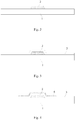
Fig. 2 is a structural schematic diagram of the metal oxide thin film transistor in which the gate electrode is prepared in an embodiment of this invention; -
Fig. 3 is a structural schematic diagram of the metal oxide thin film transistor in which the gate electrode insulating layer is prepared in an embodiment of this invention; -
Fig. 4 is a structural schematic diagram of the metal oxide thin film transistor in which the active layer is prepared in an embodiment of this invention; -
Fig. 5 is a structural schematic diagram of the metal oxide thin film transistor in which the metal nanoparticle layer is prepared in an embodiment of this invention; -
Fig. 6 is a structural schematic diagram of the metal oxide thin film transistor in which the source and drain electrode metal thin film is prepared in an embodiment of this invention; -
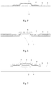
Fig. 7 is a structural schematic diagram of the metal oxide thin film transistor in which the source electrode and the drain electrode are prepared in an embodiment of this invention; -
Fig. 8 is a structural schematic diagram of the metal oxide thin film transistor in which the metal nanoparticle layer not covered by the source electrode and the drain electrode is removed in an embodiment of this invention; -
Fig. 9 is a structural schematic diagram of the metal oxide thin film transistor in which the passivation layer is prepared in an embodiment of this invention. - The processes for achieving embodiments of this invention are described below in detail in conjunction with the accompanying drawings. It is to be noted that the same or similar numerals represent the same or similar elements or elements having the same or similar functions throughout. The embodiments described below with reference to the accompanying drawings are exemplary and are merely used for explaining the present invention, and cannot be construed to be limitations of this invention.
- With reference to
Fig. 1 , an embodiment of this invention provides a preparation method of a thin film transistor, comprising: - 101, forming a gate electrode metal thin film on a base substrate, and allowing the gate electrode metal thin film to form a gate electrode metal layer comprising a gate electrode by a patterning process.
- According to different particular applications of the metal oxide thin film transistor, a glass substrate having a buffering layer may be used as the base substrate, and a flexible substrate having a water-oxygen barrier layer may also be used as the base substrate, preferably, polyethylene naphthalate, polyethylene terephthalate, a polyimide, or a metal foil is used as the material of the flexible substrate. Preferably, a SiO2 buffering layer or a Si3N4 layer is used as the buffering layer on the glass substrate. Preferably, an Al2O3 layer, a Si3N4 layer, a SiCN layer, a SiOx layer, a SiON layer, and a stacked composite structure thereof may be used as the water-oxygen barrier layer.
- Preferably, the gate electrode metal thin film is prepared by using a single film layer of any one of an aluminum thin film, a copper thin film, a molybdenum thin film, a titanium thin film, a silver thin film, a gold thin film, a tantalum thin film, a tungsten thin film, a chromium thin film, and an aluminum alloy thin film, or a composite film layer composed of at least two of the thin films, and the gate electrode metal thin film is prepared in a thickness of 100 to 2000 nanometers.
- 102, forming a gate electrode insulating layer on the gate electrode metal layer.
- Preferably, the gate electrode insulating layer is prepared by using a monolayer of a silicon oxide thin film, a silicon nitride thin film, an aluminum oxide thin film, a tantalum pentoxide thin film, or an ytterbium oxide thin film, or the gate electrode insulating layer is prepared by using a composite thin film composed of at least two monolayers of the thin films, and the gate electrode insulating layer is prepared in a thickness of 50 to 500 nanometers.
- 103, forming a metal oxide thin film on the gate electrode insulating layer, and allowing the metal oxide thin film to form a pattern of an active layer by a patterning process.
- Preferably, the active layer is prepared by using a metal oxide containing at least one of In, Zn, Ga, and Sn, and the active layer is prepared in a thickness of 10 to 200 nanometers.
- 104, preparing a metal nanoparticle layer on the active layer, said metal nanoparticle layer being used as an etching protection layer.
- Specifically, the metal nanoparticle layer may be deposited by using a process such as a physical vapor deposition, a chemical vapor deposition, a hydrothermal method, a sol-gel method, a spray pyrolysis method, a hot wall method, etc.
- The metal nanoparticle layer is prepared by using at least one material of gold nanoparticles, silver nanoparticles, platinum nanoparticles, beryllium nanoparticles, nickel nanoparticles, and cobalt nanoparticles. Preferably, the metal nanoparticle layer is prepared in a thickness of 1 to 5 nanometers. Of course, in view of cost, one or more of beryllium nanoparticles, nickel nanoparticles, and cobalt nanoparticles having lower cost may also be used for the metal nanoparticle layer.
- It is to be indicated that after the metal nanoparticle layer is deposited, it may further comprise a process of performing annealing treatment on the metal nanoparticle layer.
- In this embodiment, the active layer can be protected by the metal nanoparticle layer when the source electrode and the drain electrode are etched, so as to prevent device badness caused by the corrosion of the active layer.
- 105, forming a source and drain electrode metal thin film on the base substrate on which the above processes are finished, allowing the source and drain electrode metal thin film to form a source and drain electrode metal layer comprising a source electrode and a drain electrode by a patterning process, wherein the source electrode and the drain electrode cover a part of the metal nanoparticle layer.
- Preferably, the source and drain electrode metal thin film is prepared by using a single film layer of any one of an aluminum thin film, a copper thin film, a molybdenum thin film, and a titanium thin film, or a composite film layer composed of at least two of the thin films, and the source and drain electrode metal thin film is prepared in a thickness of 100 to 2000 nanometers.
- 106, removing or oxidizing the part of the metal nanoparticle layer which is not covered by the source electrode and the drain electrode in an oxygen-containing atmosphere.
- Preferably, removing or oxidizing the part of the metal nanoparticle layer which is not covered by the source electrode and the drain electrode is performed by using oxygen plasma.
- 107, forming a passivation layer on the source and drain electrode metal layer.
- Preferably, the passivation layer is prepared by using a single film layer of any one of silicon oxide, silicon nitride, aluminum oxide, ytterbium oxide, polyimides, benzocyclobutene, and polymethyl methacrylate, or a composite film layer composed of at least two of silicon oxide, silicon nitride, aluminum oxide, ytterbium oxide, polyimides, benzocyclobutene, and polymethyl methacrylate, and the passivation layer is prepared in a thickness of 50 to 2000 nanometers.
- It is to be indicated that a method for protecting the active layer by using an organic conductive thin film in a back channel etching process of a metal oxide thin film transistor is also provided in the prior art, but the conductivity of silicon or carbon in the organic conductive thin film is relatively poor, which may lead to bad contact of the active layer with the source electrode and the drain electrode, such that the metal oxide thin film transistor is instable; and at the meanwhile, the thermal stability of the organic conductive thin film is poor and will be decomposed in subsequent procedures, resulting in instable or bad metal oxide thin film transistors, and the decomposed organic conductive thin film may contaminate the preparation equipment. Compared to the organic conductive thin film, the metal nanoparticle layer has a better thermal stability, is capable of protecting the active layer, enables the metal oxide thin film transistor thus prepared to be more stable, and will not contaminate the preparation equipment.
- The embodiments of this invention have the advantageous effects as follows. By using the metal nanoparticle layer as a protection layer of the active layer, the active layer can be protected when the source electrode and the drain electrode are etched, so as to prevent device badness caused by the corrosion of the active layer; and at the meanwhile, the metal nanoparticle layer has a good conductivity and is favorable to the achievement of good conductive contact with the source electrode and the drain electrode; the metal nanoparticle layer has a better thermal stability compared to the organic conductive thin film, and the requirements for the preparation process of the metal oxide thin film transistor are relatively low, such that the preparation of the metal oxide thin film transistor by a simple process and a low cost is achieved.
- In order to describe the preparation method of the metal oxide thin film transistor provided by this invention in more detail, embodiments are provided in conjunction with
Fig. 2 to Fig. 9 as follows. - This embodiment of this invention provides a first particular preparation method of a metal oxide thin film transistor, comprising:
-
Step 1, depositing three layers of metal thin films of molybdenum/aluminum /molybdenum as a gate electrode metal thin film on abase substrate 1 by using a physical vapor deposition method, wherein the three layers of metal thin films of molybdenum/aluminum/molybdenum have thicknesses of 25/100/25 nanometers respectively, and allowing the gate electrode metal thin film to form agate electrode 2 by a patterning process. Thebase substrate 1 is an alkali-free glass substrate with a SiO2 buffering layer having a thickness of 200 nanometers. The schematic diagram after thegate electrode 2 is prepared on thebase substrate 1 is shown inFig. 2 . -
Step 2, depositing a gateelectrode insulating layer 3 by using a plasma enhanced chemical vapor deposition method, on thebase substrate 1 on which the above step is finished. The schematic diagram after the gateelectrode insulating layer 3 is prepared is shown inFig. 3 . - The gate electrode insulating
layer 3 is formed by laminating 300-nanometer SiNx and 30-nanometer SiO2. -
Step 3, depositing a metal oxide thin film on the gateelectrode insulating layer 3 by using a physical vapor deposition method, and allowing the metal oxide thin film to form a pattern of anactive layer 4 by a patterning process. The metal oxide thin film is an indium zinc oxide (IZO) thin film, wherein the atomic ratio of indium to zinc is 1:1. The schematic diagram in which theactive layer 4 is prepared is shown inFig. 4 . -
Step 4, depositing a gold nanoparticle layer having a thickness of 5 nanometers as ametal nanoparticle layer 5 on theactive layer 4 by using a physical vapor deposition method. The schematic diagram in which themetal nanoparticle layer 5 is prepared is shown inFig. 5 . - The
active layer 4 can be protected by themetal nanoparticle layer 5 when thesource electrode 7 and the drain electrode 8 (as shown inFig. 7 ) are subsequently etched, so as to prevent the badness of the metal oxide thin film transistor caused by the corrosion of theactive layer 4. - It is to be indicated that it may further comprise a process of annealing the
metal nanoparticle layer 5 inStep 4. -
Step 5, depositing laminated layers of molybdenum/aluminum/molybdenum, which have thicknesses of 25/100/25 nanometers respectively, as a source and drain electrode metalthin film 6 on thebase substrate 1 on which the above processes are finished, by using a physical vapor deposition method. The schematic diagram in which the source and drain electrode metalthin film 6 is prepared is shown inFig. 6 . - A mixed solution of 30% H2O2 and 1% KOH is used as a wet etching solution for etching the source and drain electrode metal
thin film 6 to form asource electrode 7 and adrain electrode 8, wherein thesource electrode 7 and thedrain electrode 8 cover a part of themetal nanoparticle layer 5. The schematic diagram in which thesource electrode 7 and thedrain electrode 8 are prepared is shown inFig. 7 . -
Step 6, removing the part of themetal nanoparticle layer 5 which is not covered by thesource electrode 7 and thedrain electrode 8 by using oxygen plasma. The schematic diagram after the part of themetal nanoparticle layer 5 not covered by thesource electrode 7 and thedrain electrode 8 is removed is shown inFig. 8 . -
Step 7, depositing 300-nanometer SiO2 as apassivation layer 9 on thebase substrate 1 on which the above processes are finished, by using a plasma enhanced chemical vapor deposition method, i.e., forming apassivation layer 9 on the source and drain electrode metal layer comprising thesource electrode 7 and thedrain electrode 8. The schematic diagram in which thepassivation layer 9 is prepared is shown inFig. 9 . - It is practically found that the protection of the
active layer 4 in the back channel etching process by using themetal nanoparticle layer 5 is more stable compared to the protection by an organic conductive thin film, and themetal nanoparticle layer 5 has a good conductivity, large surface roughness, and is very favorable to the achievement of good contact of theactive layer 4 with thesource electrode 7 and thedrain electrode 8. - This embodiment of this invention provides a second particular preparation method of a metal oxide thin film transistor, comprising:
-
Step 1, depositing a copper metal thin film as a gate electrode metal thin film on abase substrate 1 by using a physical vapor deposition method, wherein the copper metal thin film has a thickness of 500 nanometers, and allowing the gate electrode metal thin film to form agate electrode 2 by a patterning process. Thebase substrate 1 is a flexible substrate with a water-oxygen barrier layer of Al2O3 having a thickness of 50 nanometers. The schematic diagram after thegate electrode 2 is prepared on thebase substrate 1 is shown inFig. 2 . -
Step 2, depositing a gateelectrode insulating layer 3 by using a plasma enhanced chemical vapor deposition method, on thebase substrate 1 on which the above step is finished. The schematic diagram after the gateelectrode insulating layer 3 is prepared is shown inFig. 3 . - The gate electrode insulating
layer 3 is formed by laminating 200-nanometer aluminum oxide and 100-nanometer ytterbium oxide. -
Step 3, depositing a metal oxide thin film on the gateelectrode insulating layer 3 by using a physical vapor deposition method, and allowing the metal oxide thin film to form a pattern of anactive layer 4 by a patterning process. The metal oxide thin film is an 80-nanometer indium gallium zinc oxide (IGZO) thin film, wherein the atomic ratio of indium, gallium, and zinc is 1:1:1. The schematic diagram in which theactive layer 4 is prepared is shown inFig. 4 . -
Step 4, preparing a nickel nanoparticle layer having a thickness of 2 nanometers as ametal nanoparticle layer 5 on theactive layer 4, by using a spray pyrolysis method. The schematic diagram in which themetal nanoparticle layer 5 is prepared is shown inFig. 5 . - The
active layer 4 can be protected by themetal nanoparticle layer 5 when thesource electrode 7 and the drain electrode 8 (as shown inFig. 7 ) are subsequently etched, so as to prevent the badness of the metal oxide thin film transistor caused by the corrosion of theactive layer 4. - It is to be indicated that it may further comprise a process of annealing the
metal nanoparticle layer 5 inStep 4. -
Step 5, depositing a copper metal thin film having a thicknesses of 500 nanometers as a source and drain electrode metalthin film 6 on thebase substrate 1 on which the above processes are finished, by using a physical vapor deposition method. The schematic diagram in which the source and drain electrode metalthin film 6 is prepared is shown inFig. 6 . - A mixed solution of H2O2 and H2SO4 is used as a wet etching solution for etching the source and drain electrode metal
thin film 6 to form asource electrode 7 and adrain electrode 8, wherein thesource electrode 7 and thedrain electrode 8 cover a part of themetal nanoparticle layer 5. The schematic diagram in which thesource electrode 7 and thedrain electrode 8 are prepared is shown inFig. 7 . -
Step 6, removing the part of themetal nanoparticle layer 5 which is not covered by thesource electrode 7 and thedrain electrode 8 by using oxygen plasma. The schematic diagram after the part of themetal nanoparticle layer 5 not covered by thesource electrode 7 and thedrain electrode 8 is removed is shown inFig. 8 . -
Step 7, depositing 800-nanometer polyimide as apassivation layer 9 on thebase substrate 1 on which the above processes are finished, by using a plasma enhanced chemical vapor deposition method, i.e., forming apassivation layer 9 on the source and drain electrode metal layer comprising thesource electrode 7 and thedrain electrode 8. The schematic diagram in which thepassivation layer 9 is prepared is shown inFig. 9 . - It is practically found that the protection of the
active layer 4 in the back channel etching process by using themetal nanoparticle layer 5 is more stable compared to the protection by an organic conductive thin film, and the metal nanoparticle layer has a good conductivity, a rough surface, and is very favorable to the achievement of good contact of theactive layer 4 with thesource electrode 7 and thedrain electrode 8. - This embodiment of this invention provides a third particular preparation method of a metal oxide thin film transistor, comprising:
-
Step 1, depositing an ITO thin film as a gate electrode metal thin film on abase substrate 1 by using a physical vapor deposition method, wherein the ITO thin film has a thickness of 200 nanometers, and allowing the gate electrode metal thin film to form agate electrode 2 by a patterning process. Thebase substrate 1 is a flexible substrate with a water-oxygen barrier layer of Si3N4 having a thickness of 200 nanometers. The schematic diagram after thegate electrode 2 is prepared on thebase substrate 1 is shown inFig. 2 . -
Step 2, depositing a gateelectrode insulating layer 3 by using a plasma enhanced chemical vapor deposition method on thebase substrate 1 on which the above step is finished. The schematic diagram after the gateelectrode insulating layer 3 is prepared is shown inFig. 3 . - The gate electrode insulating
layer 3 is formed by laminating 100-nanometer silicon oxide, 90-nanometer tantalum pentoxide, and 20-nanometer silicon dioxide. -
Step 3, depositing a metal oxide thin film on the gateelectrode insulating layer 3 by using a physical vapor deposition method, and allowing the metal oxide thin film to form a pattern of anactive layer 4 by a patterning process. The metal oxide thin film is a 50-nanometer IZO thin film, wherein the atomic ratio of indium to zinc is 1:1. The schematic diagram in which theactive layer 4 is prepared is shown inFig. 4 . -
Step 4, preparing a silver nanoparticle layer having a thickness of 3 nanometers as ametal nanoparticle layer 5 on theactive layer 4 by using a solution treatment method. The schematic diagram in which themetal nanoparticle layer 5 is prepared is shown inFig. 5 . - The
active layer 4 can be protected by themetal nanoparticle layer 5 when thesource electrode 7 and the drain electrode 8 (as shown inFig. 7 ) are subsequently etched, so as to prevent the badness of the metal oxide thin film transistor caused by the corrosion of theactive layer 4. - It is to be indicated that it may further comprise a process of annealing the
metal nanoparticle layer 5 inStep 4. -
Step 5, depositing a copper metal thin film, which is a monolayer molybdenum thin film and has a thicknesses of 200 nanometers, as a source and drain electrode metalthin film 6 on thebase substrate 1 on which the above processes are finished, by using a physical vapor deposition method. The schematic diagram in which the source and drain electrode metalthin film 6 is prepared is shown inFig. 6 . - A mixed solution of H2O2 and H2SO4 is used as a wet etching solution for etching the source and drain electrode metal
thin film 6 to form asource electrode 7 and adrain electrode 8, wherein thesource electrode 7 and thedrain electrode 8 cover a part of themetal nanoparticle layer 5. The schematic diagram in which thesource electrode 7 and thedrain electrode 8 are prepared is shown inFig. 7 . -
Step 6, removing the part of themetal nanoparticle layer 5 which is not covered by thesource electrode 7 and thedrain electrode 8 by using oxygen plasma. The schematic diagram after the part of themetal nanoparticle layer 5 not covered by thesource electrode 7 and thedrain electrode 8 is removed is shown inFig. 8 . -
Step 7, depositing 300-nanometer SiO2 as apassivation layer 9 on thebase substrate 1 on which the above processes are finished, by using a plasma enhanced chemical vapor deposition method, i.e., forming apassivation layer 9 on the source and drain electrode metal layer comprising thesource electrode 7 and thedrain electrode 8. The schematic diagram in which thepassivation layer 9 is prepared is shown inFig. 9 . - It is practically found that the protection of the
active layer 4 in the back channel etching process by using themetal nanoparticle layer 5 is more stable compared to the protection by an organic conductive thin film, and the metal nanoparticle layer has a good conductivity, a rough surface, and is very favorable to the achievement of good contact of theactive layer 4 with thesource electrode 7 and thedrain electrode 8. - The
above embodiments 1 to 3 are merely a part of specific embodiments provided to illustrate this invention, and this invention is not limited thereto. The prepared metal oxide thin film transistors may be used in liquid crystal displays and active matrix organic light-emitting diode displays. Thicknesses of thin films, constituent materials, proportioning ratios, etc., involved in each step inembodiments 1 to 3 may be adjusted according to practical requirements. - As shown in
Fig. 9 , one embodiment of this invention further provides a thin film transistor, which is a metal oxide thin film transistor, comprising: - a
base substrate 1; - a gate electrode metal layer formed on the
base substrate 1, wherein the gate electrode metal layer comprises agate electrode 2; - a gate
electrode insulating layer 3 formed on the gate electrode metal layer; - an
active layer 4 formed on the gate electrode insulating layer; - a
metal nanoparticle layer 5 formed on theactive layer 4, wherein themetal nanoparticle layer 5 is used as an etching protection layer; - a source and drain electrode metal layer formed on the
metal nanoparticle layer 5, wherein the source and drain electrode metal layer comprises asource electrode 7 and adrain electrode 8; and - a
passivation layer 9 formed on the source and drain electrode metal layer. - It is to be indicated that the part indicated by the dashed
frame 10 is the removed part ofmetal nanoparticle layer 5, which is removed after thesource electrode 7 and thedrain electrode 8 are formed. This part of themetal nanoparticle layer 5, which should be removed, can protect theactive layer 4 when thesource electrode 7 and thedrain electrode 8 are prepared. - Preferably, the
metal nanoparticle layer 5 comprises at least one material of gold nanoparticles, silver nanoparticles, platinum nanoparticles, beryllium nanoparticles, nickel nanoparticles, and cobalt nanoparticles. - Preferably, the
metal nanoparticle layer 5 has a thickness of 1 to 5 nanometers. - Preferably, the
base substrate 1 is a glass substrate having a buffering layer. - Preferably, the
base substrate 1 is a flexible substrate having a water-oxygen barrier layer, and the material of the flexible substrate is polyethylene naphthalate, polyethylene terephthalate, a polyimide, or a metal foil. - Preferably, the gate electrode metal layer is a single film layer of any one of an aluminum thin film, a copper thin film, a molybdenum thin film, a titanium thin film, a silver thin film, a gold thin film, a tantalum thin film, a tungsten thin film, a chromium thin film, and an aluminum alloy thin film, or a composite film layer composed of at least two of the thin films, and the gate electrode metal layer has a thickness of 100 to 2000 nanometers. It is to be indicated that the material and the thickness of the gate electrode metal layer herein are those of the gate electrode metal thin film in the preparation method.
- Preferably, the gate
electrode insulating layer 3 is a monolayer of a silicon oxide thin film, a silicon nitride thin film, an aluminum oxide thin film, a tantalum pentoxide thin film, or an ytterbium oxide thin film, or the gateelectrode insulating layer 3 is a composite thin film composed of at least two monolayers of the thin films, and the gateelectrode insulating layer 3 has a thickness of 50 to 500 nanometer. - Preferably, the
active layer 4 contains a metal oxide of at least one of In, Zn, Ga, and Sn, theactive layer 4 has a thickness of 10 to 200 nanometers. - Preferably, the source and drain electrode metal layer is a single film layer of any one of an aluminum thin film, a copper thin film, a molybdenum thin film, and a titanium thin film, or a composite film layer composed of at least two of the thin films, the source and drain electrode metal layer has a thickness of 100 to 2000 nanometers. It is to be indicated that the material and the thickness of the source and drain electrode metal layer herein are those of the source and drain electrode metal thin film in the preparation method.
- Preferably, the
passivation layer 9 may be a single film layer of any one of silicon oxide, silicon nitride, aluminum oxide, ytterbium oxide, polyimides, benzocyclobutene, and polymethyl methacrylate, or a composite film layer composed of at least two of silicon oxide, silicon nitride, aluminum oxide, ytterbium oxide, polyimides, benzocyclobutene, and polymethyl methacrylate. Preferably, thepassivation layer 9 has a thickness of 50 to 2000 nanometers. - The embodiment of this invention has the advantageous effects as follows. By using the metal nanoparticle layer as a protection layer of the active layer, the active layer can be protected when the source electrode and the drain electrode are etched, so as to prevent device badness caused by the corrosion of the active layer; and at the meanwhile, the metal nanoparticle layer has a good conductivity and good thermal stability, and the requirements for the preparation process of the metal oxide thin film transistor are relatively low, such that the preparation of the metal oxide thin film transistor by a simple process and a low cost is achieved.
- Based on the same inventive concept, one embodiment of this invention further provides an array substrate, comprising the thin film transistor as provided by the above embodiment.
- The embodiment of this invention has the advantageous effects as follows. In this array substrate, the metal oxide thin film transistor uses the metal nanoparticle layer as a protection layer of the active layer, and the active layer can be protected when the source electrode and the drain electrode are etched, so as to prevent device badness caused by the corrosion of the active layer; and at the meanwhile, the metal nanoparticle layer has a good conductivity and good thermal stability, and the requirements for the preparation process of the metal oxide thin film transistor are relatively low, such that the preparation of the metal oxide thin film transistor by a simple process and a low cost is achieved.
- Based on the same inventive concept, one embodiment of this invention provides a display panel, comprising the array substrate as provided by the above embodiment.
- The embodiment of this invention has the advantageous effects as follows. In the array substrate used by the display panel, the metal oxide thin film transistor uses the metal nanoparticle layer as a protection layer of the active layer, and the active layer can be protected when the source electrode and the drain electrode are etched, so as to prevent device badness caused by the corrosion of the active layer; and at the meanwhile, the metal nanoparticle layer has a good conductivity and good thermal stability, and the requirements for the preparation process of the metal oxide thin film transistor are relatively low, such that the preparation of the metal oxide thin film transistor by a simple process and a low cost is achieved.
- Obviously, a person skilled in the art may perform various modifications and variations on this invention without departing from the spirit and the scope of this invention. Thus, if these modifications and variations of the invention are within the scope of the claims of this invention and equivalent techniques thereof, this invention also intends to encompass these modifications and variations.
Claims (15)
- A preparation method of a thin film transistor, characterized by comprising:forming a gate electrode metal thin film on a base substrate, and allowing the gate electrode metal thin film to form a gate electrode metal layer comprising a gate electrode by a patterning process;forming a gate electrode insulating layer on the gate electrode metal layer;forming a metal oxide thin film on the gate electrode insulating layer, and allowing the metal oxide thin film to form a pattern of an active layer by a patterning process;preparing a metal nanoparticle layer on the active layer, said metal nanoparticle layer being used as an etching protection layer;forming a source and drain electrode metal thin film on the base substrate on which the above processes are finished, and allowing the source and drain electrode metal thin film to form a source and drain electrode metal layer comprising a source electrode and a drain electrode by a patterning process, wherein the source electrode and the drain electrode cover a part of the metal nanoparticle layer;removing or oxidizing the part of the metal nanoparticle layer which is not covered by the source electrode and the drain electrode in an oxygen-containing atmosphere; andforming a passivation layer on the source and drain electrode metal layer.
- The preparation method as claimed in claim 1, characterized in that the metal nanoparticle layer is prepared by using at least one material of gold nanoparticles, silver nanoparticles, platinum nanoparticles, beryllium nanoparticles, nickel nanoparticles, and cobalt nanoparticles.
- The preparation method as claimed in claim 2, characterized in that preparing the metal nanoparticle layer on the active layer comprises:preparing the metal nanoparticle layer on the active layer by using a physical vapor deposition, a chemical vapor deposition, a hydrothermal method, a sol-gel method, a spray pyrolysis method, or a hot wall method.
- The preparation method as claimed in claim 2, characterized in that the metal nanoparticle layer is prepared in a thickness of 1 to 5 nanometers.
- The preparation method as claimed in any one of claims 1 to 4, characterized in that a glass substrate having a buffering layer is used as the base substrate.
- The preparation method as claimed in any one of claims 1 to 4, characterized in that a flexible substrate having a water-oxygen barrier layer is used as the base substrate, and polyethylene naphthalate, polyethylene terephthalate, a polyimide, or a metal foil is used as the material of the flexible substrate.
- The preparation method according to any one of claims 1 to 4, characterized in that the gate electrode metal thin film is prepared by using a single film layer of any one of an aluminum thin film, a copper thin film, a molybdenum thin film, a titanium thin film, a silver thin film, a gold thin film, a tantalum thin film, a tungsten thin film, a chromium thin film, and an aluminum alloy thin film, or a composite film layer composed of at least two of the thin films, and the gate electrode metal thin film is prepared in a thickness of 100 to 2000 nanometers.
- The preparation method according to any one of claims 1 to 4, characterized in that the gate electrode insulating layer is prepared by using a monolayer of a silicon oxide thin film, a silicon nitride thin film, an aluminum oxide thin film, a tantalum pentoxide thin film, or an ytterbium oxide thin film, or the gate electrode insulating layer is prepared by using a composite thin film composed of at least two monolayers of the thin films, and the gate electrode insulating layer is prepared in a thickness of 50 to 500 nanometers.
- The preparation method according to any one of claims 1 to 4, characterized in that the active layer is prepared by using a metal oxide containing at least one of In, Zn, Ga, and Sn, and the active layer is prepared in a thickness of 10 to 200 nanometers.
- The preparation method according to any one of claims 1 to 4, characterized in that the source and drain electrode metal thin film is prepared by using a single film layer of any one of an aluminum thin film, a copper thin film, a molybdenum thin film, and a titanium thin film, or a composite film layer composed of at least two of the thin films, and the source and drain electrode metal thin film is prepared in a thickness of 100 to 2000 nanometers.
- The preparation method as claimed in claim 1, characterized in that removing or oxidizing the part of the metal nanoparticle layer which is not covered by the source electrode and the drain electrode is performed by using oxygen plasma.
- The preparation method as claimed in claim 1, characterized in that the passivation layer is prepared by using a single film layer of any one of silicon oxide, silicon nitride, aluminum oxide, ytterbium oxide, polyimide, benzocyclobutene, and polymethyl methacrylate, or a composite film layer composed of at least two of silicon oxide, silicon nitride, aluminum oxide, ytterbium oxide, polyimide, benzocyclobutene, andpolymethyl methacrylate, and the passivation layer is prepared in a thickness of 50 to 2000 nanometers.
- A thin film transistor, characterized by comprising:a base substrate;a gate electrode metal layer formed on the base substrate, wherein the gate electrode metal layer comprises a gate electrode;a gate electrode insulating layer formed on the gate electrode metal layer;an active layer formed on the gate electrode insulating layer;a metal nanoparticle layer formed on the active layer, wherein the metal nanoparticle layer is used as an etching protection layer;a source and drain electrode metal layer formed on the metal nanoparticle layer, wherein the source and drain electrode metal layer comprises a source electrode and a drain electrode; anda passivation layer formed on the source and drain electrode metal layer.
- An array substrate, characterized by comprising the thin film transistor as claimed in claim 13.
- A display panel, characterized by comprising an array substrate according to claim 14.
Applications Claiming Priority (2)
| Application Number | Priority Date | Filing Date | Title |
|---|---|---|---|
| CN201510232985.5A CN104934330A (en) | 2015-05-08 | 2015-05-08 | Film transistor and preparation method thereof, array substrate and display panel |
| PCT/CN2015/091540 WO2016179951A1 (en) | 2015-05-08 | 2015-10-09 | Thin-film transistor and preparation method therefor, array substrate, and display panel |
Publications (3)
| Publication Number | Publication Date |
|---|---|
| EP3121840A1 true EP3121840A1 (en) | 2017-01-25 |
| EP3121840A4 EP3121840A4 (en) | 2017-11-22 |
| EP3121840B1 EP3121840B1 (en) | 2020-08-12 |
Family
ID=54121439
Family Applications (1)
| Application Number | Title | Priority Date | Filing Date |
|---|---|---|---|
| EP15882903.6A Active EP3121840B1 (en) | 2015-05-08 | 2015-10-09 | Thin-film transistor and preparation method therefor, array substrate, and display panel |
Country Status (4)
| Country | Link |
|---|---|
| US (1) | US20170154905A1 (en) |
| EP (1) | EP3121840B1 (en) |
| CN (1) | CN104934330A (en) |
| WO (1) | WO2016179951A1 (en) |
Families Citing this family (30)
| Publication number | Priority date | Publication date | Assignee | Title |
|---|---|---|---|---|
| CN104934330A (en) * | 2015-05-08 | 2015-09-23 | 京东方科技集团股份有限公司 | Film transistor and preparation method thereof, array substrate and display panel |
| WO2018076285A1 (en) * | 2016-10-28 | 2018-05-03 | 深圳市柔宇科技有限公司 | Array substrate and method for manufacturing same |
| CN109906376B (en) * | 2016-11-02 | 2021-08-10 | 株式会社Lg化学 | Gas detection sensor |
| CN106773205B (en) * | 2016-12-26 | 2019-09-17 | 京东方科技集团股份有限公司 | Display panel and preparation method thereof and display device |
| CN107833927A (en) * | 2017-11-16 | 2018-03-23 | 佛山科学技术学院 | A kind of oxide thin film transistor and preparation method thereof |
| CN110010695B (en) * | 2018-01-05 | 2021-09-17 | 京东方科技集团股份有限公司 | Thin film transistor, array substrate, manufacturing method of array substrate and display panel |
| CN108198824B (en) * | 2018-01-17 | 2020-06-16 | 京东方科技集团股份有限公司 | A kind of preparation method of array substrate |
| KR20200126428A (en) * | 2018-03-27 | 2020-11-06 | 코닝 인코포레이티드 | Method of forming thin film transistor on glass substrate and liquid crystal display formed therefrom |
| CN108615735B (en) * | 2018-05-03 | 2021-01-22 | 京东方科技集团股份有限公司 | Array substrate, display device and manufacturing method of array substrate |
| CN109755259B (en) * | 2018-12-21 | 2021-12-17 | 惠科股份有限公司 | Display panel manufacturing method and display panel |
| CN109920855B (en) * | 2019-02-13 | 2020-11-03 | 深圳市华星光电半导体显示技术有限公司 | Thin film transistor and manufacturing method thereof |
| CN109991787B (en) * | 2019-03-15 | 2022-06-07 | 惠科股份有限公司 | Array substrate and manufacturing method thereof |
| CN109991772B (en) * | 2019-03-29 | 2023-03-14 | 广州国显科技有限公司 | Display panel film structure and preparation process thereof |
| TWI690060B (en) | 2019-04-25 | 2020-04-01 | 元太科技工業股份有限公司 | Memory structure and manufacturing method thereof |
| CN110520976B (en) * | 2019-07-16 | 2024-02-09 | 京东方科技集团股份有限公司 | Display substrate, manufacturing method thereof and display device |
| CN110610867A (en) * | 2019-08-20 | 2019-12-24 | 深圳市华星光电技术有限公司 | Thin film transistor preparation method and thin film transistor |
| WO2021097733A1 (en) * | 2019-11-21 | 2021-05-27 | 重庆康佳光电技术研究院有限公司 | Thin film transistor and manufacturing method therefor, and thin film transistor array |
| CN111524915B (en) * | 2020-04-28 | 2022-07-12 | 深圳市华星光电半导体显示技术有限公司 | Thin film transistor device and manufacturing method thereof |
| CN111584517A (en) * | 2020-05-15 | 2020-08-25 | Tcl华星光电技术有限公司 | Array substrate and preparation method thereof |
| CN112736033B (en) * | 2020-12-24 | 2023-04-18 | 吉林建筑大学 | Method for preparing large-batch p-type thin film transistors on protein substrate |
| CN112687554B (en) * | 2020-12-28 | 2023-05-09 | 深圳市华星光电半导体显示技术有限公司 | Array substrate preparation method, array substrate and display device |
| CN112701046B (en) | 2020-12-29 | 2021-11-23 | 华南理工大学 | Passivation layer and preparation method thereof, flexible thin film transistor and preparation method thereof, and array substrate |
| CN113097134B (en) * | 2021-04-09 | 2022-07-15 | 广州新视界光电科技有限公司 | Method for preparing an array substrate and array substrate |
| CN115708202A (en) * | 2021-08-20 | 2023-02-21 | 咸阳虹微新型显示技术有限公司 | Polycrystalline silicon thin film transistor, manufacturing method thereof and array substrate |
| CN114141787B (en) * | 2021-10-27 | 2025-04-29 | 重庆惠科金渝光电科技有限公司 | Array substrate and preparation method thereof, and display panel |
| CN114530461B (en) * | 2022-02-11 | 2026-06-16 | 广州华星光电半导体显示技术有限公司 | Display panel and its manufacturing method |
| CN114709173B (en) * | 2022-03-30 | 2026-02-13 | 广州华星光电半导体显示技术有限公司 | Array substrate and its fabrication method, display panel |
| CN114959397B (en) * | 2022-04-28 | 2023-04-07 | 长沙惠科光电有限公司 | Alloy target material, preparation method and application thereof, and array substrate |
| CN115565885A (en) * | 2022-09-28 | 2023-01-03 | 吉林建筑大学 | A method for preparing thin film transistors on corn protein substrates |
| CN115842047A (en) * | 2022-11-30 | 2023-03-24 | 西安交通大学 | Schottky barrier field effect transistor and preparation method thereof |
Family Cites Families (105)
| Publication number | Priority date | Publication date | Assignee | Title |
|---|---|---|---|---|
| US6331356B1 (en) * | 1989-05-26 | 2001-12-18 | International Business Machines Corporation | Patterns of electrically conducting polymers and their application as electrodes or electrical contacts |
| JPH053319A (en) * | 1991-06-25 | 1993-01-08 | Canon Inc | Thin film semiconductor device and manufacturing method thereof |
| US5776425A (en) * | 1995-04-26 | 1998-07-07 | National Science Council | Method for preparing porous tin oxide monolith with high specific surface area and controlled degree of transparency |
| JP4511092B2 (en) * | 2000-12-11 | 2010-07-28 | セイコーエプソン株式会社 | Manufacturing method of semiconductor device |
| KR100379824B1 (en) * | 2000-12-20 | 2003-04-11 | 엘지.필립스 엘시디 주식회사 | Etchant and array substrate for electric device with Cu lines patterend on the array substrate using the etchant |
| US6679938B1 (en) * | 2001-01-26 | 2004-01-20 | University Of Maryland | Method of producing metal particles by spray pyrolysis using a co-solvent and apparatus therefor |
| US20030113550A1 (en) * | 2001-09-14 | 2003-06-19 | Millett Frederick A. | Heat barrier window utilizing a combination of coatings |
| DE10153563A1 (en) * | 2001-10-30 | 2003-05-15 | Infineon Technologies Ag | Semiconductor device fabrication method, involves constructing pair of bodies of organic semiconductor and electrically conductive contact material and doping by activated nanoparticles |
| KR100415617B1 (en) * | 2001-12-06 | 2004-01-24 | 엘지.필립스 엘시디 주식회사 | Etchant and method of fabricating metal wiring and thin film transistor using the same |
| KR100866976B1 (en) * | 2002-09-03 | 2008-11-05 | 엘지디스플레이 주식회사 | Array substrate for LCD and manufacturing method |
| US20040086807A1 (en) * | 2002-11-06 | 2004-05-06 | Chih-Yu Peng | Method of fabricating thin film transistor |
| US7090783B1 (en) * | 2003-03-13 | 2006-08-15 | Louisiana Tech University Research Foundation As A Division Of The Louisiana Tech University Foundation | Lithography-based patterning of layer-by-layer nano-assembled thin films |
| KR100602062B1 (en) * | 2003-04-03 | 2006-07-14 | 엘지.필립스 엘시디 주식회사 | Horizontal field applied liquid crystal display device and manufacturing method thereof |
| US7005752B2 (en) * | 2003-10-20 | 2006-02-28 | Texas Instruments Incorporated | Direct bumping on integrated circuit contacts enabled by metal-to-insulator adhesion |
| US7276389B2 (en) * | 2004-02-25 | 2007-10-02 | Samsung Electronics Co., Ltd. | Article comprising metal oxide nanostructures and method for fabricating such nanostructures |
| US7507618B2 (en) * | 2005-06-27 | 2009-03-24 | 3M Innovative Properties Company | Method for making electronic devices using metal oxide nanoparticles |
| JP2007123773A (en) * | 2005-10-31 | 2007-05-17 | Fuji Electric Holdings Co Ltd | Thin film transistor and manufacturing method thereof |
| JP4997750B2 (en) * | 2005-12-12 | 2012-08-08 | 富士通株式会社 | Electronic device using carbon nanotube and method for manufacturing the same |
| CN100374194C (en) * | 2006-07-19 | 2008-03-12 | 北京工业大学 | Preparation method and equipment of inorganic oxide or metal nanoparticle |
| KR20080008562A (en) * | 2006-07-20 | 2008-01-24 | 삼성전자주식회사 | Manufacturing Method of Array Substrate, Array Substrate and Display Device Having Same |
| US7919795B2 (en) * | 2006-12-21 | 2011-04-05 | Samsung Electronics Co., Ltd. | Wire structure, method for fabricating wire, thin film transistor substrate, and method for fabricating the thin film transistor substrate |
| TWI345835B (en) * | 2007-01-02 | 2011-07-21 | Chunghwa Picture Tubes Ltd | Organic thin film transistor and method for manufacturing thereof |
| KR101325053B1 (en) * | 2007-04-18 | 2013-11-05 | 삼성디스플레이 주식회사 | Thin film transistor substrate and manufacturing method thereof |
| US20080296567A1 (en) * | 2007-06-04 | 2008-12-04 | Irving Lyn M | Method of making thin film transistors comprising zinc-oxide-based semiconductor materials |
| US8207010B2 (en) * | 2007-06-05 | 2012-06-26 | Semiconductor Energy Laboratory Co., Ltd. | Method for manufacturing photoelectric conversion device |
| KR100934260B1 (en) * | 2007-09-14 | 2009-12-28 | 삼성모바일디스플레이주식회사 | Thin film transistor and its manufacturing method, organic light emitting display device and its manufacturing method and donor substrate for laser thermal transfer method |
| TWI348766B (en) * | 2007-10-04 | 2011-09-11 | Taiwan Tft Lcd Ass | Method of fabricating thin film transistor |
| WO2009060922A1 (en) * | 2007-11-05 | 2009-05-14 | Semiconductor Energy Laboratory Co., Ltd. | Thin film transistor and display device having the thin film transistor |
| US8048488B2 (en) * | 2008-01-14 | 2011-11-01 | Xerox Corporation | Methods for removing a stabilizer from a metal nanoparticle using a destabilizer |
| KR100958006B1 (en) * | 2008-06-18 | 2010-05-17 | 삼성모바일디스플레이주식회사 | Thin film transistor, its manufacturing method, and flat panel display device comprising thin film transistor |
| JP2010027783A (en) * | 2008-07-17 | 2010-02-04 | Sharp Corp | Wiring substrate and display device |
| TWI469354B (en) * | 2008-07-31 | 2015-01-11 | 半導體能源研究所股份有限公司 | Semiconductor device and method of manufacturing same |
| US8784702B2 (en) * | 2008-08-11 | 2014-07-22 | Osaka Municipal Technical Research Institute | Copper-containing nanoparticles and manufacturing method therefor |
| KR101616703B1 (en) * | 2008-08-11 | 2016-04-29 | 지호우 도쿠리츠 교세이 호진 오사카 시리츠 고교 겐큐쇼 | Composite nanoparticle and process for producing same |
| KR101911386B1 (en) * | 2008-09-19 | 2018-12-19 | 가부시키가이샤 한도오따이 에네루기 켄큐쇼 | Display device |
| JP5560281B2 (en) * | 2008-11-17 | 2014-07-23 | アイメック | Solution processing method for forming electrical contacts of organic devices |
| JP4752927B2 (en) * | 2009-02-09 | 2011-08-17 | ソニー株式会社 | Thin film transistor and display device |
| US8247276B2 (en) * | 2009-02-20 | 2012-08-21 | Semiconductor Energy Laboratory Co., Ltd. | Thin film transistor, method for manufacturing the same, and semiconductor device |
| US20100233361A1 (en) * | 2009-03-12 | 2010-09-16 | Xerox Corporation | Metal nanoparticle composition with improved adhesion |
| US8236599B2 (en) * | 2009-04-09 | 2012-08-07 | State of Oregon acting by and through the State Board of Higher Education | Solution-based process for making inorganic materials |
| WO2010123735A1 (en) * | 2009-04-24 | 2010-10-28 | Nanosys, Inc. | Nanoparticle plasmon scattering layer for photovoltaic cells |
| WO2011001715A1 (en) * | 2009-06-29 | 2011-01-06 | シャープ株式会社 | Oxide semiconductor, thin-film transistor array substrate and manufacturing method therefor, and display device |
| US8512603B2 (en) * | 2009-08-04 | 2013-08-20 | Precursor Energetics, Inc. | Polymeric precursors for CIS and CIGS photovoltaics |
| US20110059233A1 (en) * | 2009-09-04 | 2011-03-10 | Xerox Corporation | Method For Preparing Stabilized Metal Nanoparticles |
| WO2011043164A1 (en) * | 2009-10-09 | 2011-04-14 | Semiconductor Energy Laboratory Co., Ltd. | Semiconductor device and method for manufacturing the semiconductor device |
| KR101820973B1 (en) * | 2009-10-09 | 2018-01-22 | 가부시키가이샤 한도오따이 에네루기 켄큐쇼 | Semiconductor device and method for manufacturing the semiconductor device |
| KR101876470B1 (en) * | 2009-11-06 | 2018-07-10 | 가부시키가이샤 한도오따이 에네루기 켄큐쇼 | Semiconductor device |
| FR2952384B1 (en) * | 2009-11-10 | 2012-12-14 | Commissariat Energie Atomique | SELECTIVE DEPOSITION OF NANOPARTICLES |
| WO2011068028A1 (en) * | 2009-12-04 | 2011-06-09 | Semiconductor Energy Laboratory Co., Ltd. | Semiconductor element, semiconductor device, and method for manufacturing the same |
| WO2011074336A1 (en) * | 2009-12-17 | 2011-06-23 | シャープ株式会社 | Active matrix substrate and method for producing same |
| US20130026462A1 (en) * | 2010-03-04 | 2013-01-31 | Sharp Kabushiki Kaisha | Method for manufacturing thin film transistor and thin film transistor manufactured by the same, and active matrix substrate |
| US20130037807A1 (en) * | 2010-03-11 | 2013-02-14 | Sharp Kabushiki Kaisha | Semiconductor device and method for manufacturing the same |
| WO2011127095A2 (en) * | 2010-04-05 | 2011-10-13 | Gonano Technologies, Inc. | Catalytic converters, insert materials for catalytic converters, and methods of making |
| WO2011125275A1 (en) * | 2010-04-06 | 2011-10-13 | シャープ株式会社 | Thin film transistor substrate and method for manufacturing same |
| US8450236B2 (en) * | 2010-04-13 | 2013-05-28 | Cristal Usa Inc. | Supported precious metal catalysts via hydrothermal deposition |
| KR101877377B1 (en) * | 2010-04-23 | 2018-07-11 | 가부시키가이샤 한도오따이 에네루기 켄큐쇼 | Manufacturing method of semiconductor device |
| US20110263079A1 (en) * | 2010-04-23 | 2011-10-27 | Applies Materials, Inc. | Interface protection layaer used in a thin film transistor structure |
| JP5133469B2 (en) * | 2010-06-08 | 2013-01-30 | シャープ株式会社 | Thin film transistor substrate, liquid crystal display device including the same, and method for manufacturing thin film transistor substrate |
| FR2961219B1 (en) * | 2010-06-09 | 2012-07-13 | Essilor Int | PROCESS FOR THE LOW TEMPERATURE PREPARATION OF ELECTROCONDUCTIVE MESOSTRUCTURE COATINGS |
| US8765025B2 (en) * | 2010-06-09 | 2014-07-01 | Xerox Corporation | Silver nanoparticle composition comprising solvents with specific hansen solubility parameters |
| US9368599B2 (en) * | 2010-06-22 | 2016-06-14 | International Business Machines Corporation | Graphene/nanostructure FET with self-aligned contact and gate |
| US8158032B2 (en) * | 2010-08-20 | 2012-04-17 | Xerox Corporation | Silver nanoparticle ink composition for highly conductive features with enhanced mechanical properties |
| US8664097B2 (en) * | 2010-09-13 | 2014-03-04 | Semiconductor Energy Laboratory Co., Ltd. | Manufacturing method of semiconductor device |
| JP6080167B2 (en) * | 2010-10-01 | 2017-02-15 | アプライド マテリアルズ インコーポレイテッドApplied Materials,Incorporated | Materials based on gallium arsenide used in thin film transistor applications |
| PT105340A (en) * | 2010-10-18 | 2012-04-18 | Innovnano Materiais Avancados S A | CONTINUOUS PROCESS OF SYNTHESIS OF NANOMATERIALS FROM EMULSIFICATION AND DETONATION SIMULTANEOUSLY OF AN EMULSION |
| KR101789586B1 (en) * | 2010-12-06 | 2017-10-26 | 삼성디스플레이 주식회사 | Light-scattering substrate, manufacturing method thereof, Organic light emitting display device comprising thereof and manufancturing method of the organic light emitting display device |
| KR101843871B1 (en) * | 2011-03-11 | 2018-04-02 | 삼성디스플레이 주식회사 | Thin film transistor array panel and manufacturing method thereof |
| US8586134B2 (en) * | 2011-05-06 | 2013-11-19 | Xerox Corporation | Method of fabricating high-resolution features |
| KR101934977B1 (en) * | 2011-08-02 | 2019-03-19 | 삼성디스플레이 주식회사 | Thin film transistor array panel and manufacturing method thereof |
| TWI491050B (en) * | 2011-11-25 | 2015-07-01 | 新力股份有限公司 | Transistors, displays and electronic devices |
| US8916424B2 (en) * | 2012-02-07 | 2014-12-23 | Semiconductor Energy Laboratory Co., Ltd. | Method for manufacturing semiconductor device |
| US20130207111A1 (en) * | 2012-02-09 | 2013-08-15 | Semiconductor Energy Laboratory Co., Ltd. | Semiconductor device, display device including semiconductor device, electronic device including semiconductor device, and method for manufacturing semiconductor device |
| TWI474409B (en) * | 2012-02-14 | 2015-02-21 | 群康科技(深圳)有限公司 | Thin film transistor, manufacturing method thereof and display |
| US8940197B2 (en) * | 2012-02-24 | 2015-01-27 | Xerox Corporation | Processes for producing palladium nanoparticle inks |
| JP2013201211A (en) * | 2012-03-23 | 2013-10-03 | Sony Corp | Thin film transistor, manufacturing method of thin film transistor, and electronic equipment |
| US20150171220A1 (en) * | 2012-05-28 | 2015-06-18 | Sharp Kabushiki Kaisha | Semiconductor device and method for manufacturing same |
| WO2014004228A1 (en) * | 2012-06-27 | 2014-01-03 | 3M Innovative Properties Company | Optical component array |
| WO2014004789A2 (en) * | 2012-06-27 | 2014-01-03 | Precursor Energetics, Inc. | Molecular precursors for synthesis of lithium-iron-containing cathode materials |
| JP6006558B2 (en) * | 2012-07-17 | 2016-10-12 | 株式会社半導体エネルギー研究所 | Semiconductor device and manufacturing method thereof |
| US9437892B2 (en) * | 2012-07-26 | 2016-09-06 | Quswami, Inc. | System and method for converting chemical energy into electrical energy using nano-engineered porous network materials |
| JP2014032999A (en) * | 2012-08-01 | 2014-02-20 | Panasonic Liquid Crystal Display Co Ltd | Thin film transistor and manufacturing method thereof |
| JP6078920B2 (en) * | 2013-02-13 | 2017-02-15 | 国立大学法人広島大学 | Thin film forming method, and semiconductor substrate and electronic device manufactured using the same |
| CN103236443B (en) * | 2013-05-14 | 2014-05-14 | 广州新视界光电科技有限公司 | Metal oxide thin film transistor and preparation method thereof |
| US9105373B2 (en) * | 2013-06-19 | 2015-08-11 | Xerox Corporation | Safe method for manufacturing silver nanoparticle inks |
| KR102290801B1 (en) * | 2013-06-21 | 2021-08-17 | 가부시키가이샤 한도오따이 에네루기 켄큐쇼 | Semiconductor device and manufacturing method thereof |
| JP6264090B2 (en) * | 2013-07-31 | 2018-01-24 | 株式会社リコー | FIELD EFFECT TRANSISTOR AND METHOD FOR MANUFACTURING FIELD EFFECT TRANSISTOR |
| TWI487625B (en) * | 2013-08-22 | 2015-06-11 | Ind Tech Res Inst | Metal oxide multilayered structure for infrared blocking |
| JP6135427B2 (en) * | 2013-09-27 | 2017-05-31 | 凸版印刷株式会社 | Thin film transistor array and manufacturing method thereof |
| US10144066B2 (en) * | 2013-11-20 | 2018-12-04 | National University Corporation Yamagata University | Silver nanoparticles, method for producing silver nanoparticles, and silver nanoparticle ink |
| JP5924609B2 (en) * | 2013-12-03 | 2016-05-25 | 国立大学法人山形大学 | Method for producing metal thin film and method for producing conductive structure |
| CN103730414B (en) * | 2013-12-31 | 2016-02-24 | 深圳市华星光电技术有限公司 | The manufacture method of thin film transistor base plate |
| CN103972299B (en) * | 2014-04-28 | 2016-03-30 | 京东方科技集团股份有限公司 | A kind of thin-film transistor and preparation method thereof, display base plate, display unit |
| CN104241392B (en) * | 2014-07-14 | 2017-07-14 | 京东方科技集团股份有限公司 | A kind of thin film transistor (TFT) and preparation method thereof, display base plate and display device |
| TWI566388B (en) * | 2014-08-12 | 2017-01-11 | 群創光電股份有限公司 | Display panel |
| CN104241394A (en) * | 2014-08-29 | 2014-12-24 | 京东方科技集团股份有限公司 | A kind of thin film transistor and corresponding preparation method, display substrate and display device |
| US9634145B2 (en) * | 2014-10-29 | 2017-04-25 | Eastman Kodak Company | TFT substrate with variable dielectric thickness |
| KR102328917B1 (en) * | 2014-09-22 | 2021-11-19 | 엘지디스플레이 주식회사 | Organic light emitting diode display device |
| US9738807B2 (en) * | 2014-10-08 | 2017-08-22 | Kabushiki Kaisha Toshiba | Method of forming pattern and pattern |
| CN104409515A (en) * | 2014-11-26 | 2015-03-11 | 京东方科技集团股份有限公司 | Oxide film transistor and manufacturing method thereof, array substrate and display device |
| WO2016084699A1 (en) * | 2014-11-28 | 2016-06-02 | シャープ株式会社 | Semiconductor device and production method therefor |
| CN104716198B (en) * | 2015-03-25 | 2018-03-27 | 京东方科技集团股份有限公司 | Thin film transistor (TFT) and its manufacture method, display device |
| CN104934330A (en) * | 2015-05-08 | 2015-09-23 | 京东方科技集团股份有限公司 | Film transistor and preparation method thereof, array substrate and display panel |
| CN104779302A (en) * | 2015-05-11 | 2015-07-15 | 京东方科技集团股份有限公司 | Thin film transistor and manufacturing method, array substrate and display device thereof |
| US20170218529A1 (en) * | 2016-01-28 | 2017-08-03 | Johnson Matthey Public Limited Company | Cathode material |
| JP2017143108A (en) * | 2016-02-08 | 2017-08-17 | 株式会社ジャパンディスプレイ | Thin film transistor and method of manufacturing thin film transistor |
-
2015
- 2015-05-08 CN CN201510232985.5A patent/CN104934330A/en active Pending
- 2015-10-09 US US15/122,155 patent/US20170154905A1/en not_active Abandoned
- 2015-10-09 WO PCT/CN2015/091540 patent/WO2016179951A1/en not_active Ceased
- 2015-10-09 EP EP15882903.6A patent/EP3121840B1/en active Active
Also Published As
| Publication number | Publication date |
|---|---|
| CN104934330A (en) | 2015-09-23 |
| EP3121840A4 (en) | 2017-11-22 |
| WO2016179951A1 (en) | 2016-11-17 |
| EP3121840B1 (en) | 2020-08-12 |
| US20170154905A1 (en) | 2017-06-01 |
Similar Documents
| Publication | Publication Date | Title |
|---|---|---|
| EP3121840B1 (en) | Thin-film transistor and preparation method therefor, array substrate, and display panel | |
| US9960260B2 (en) | Metal oxide thin film transistor and a preparation method thereof | |
| US10186674B2 (en) | Thin-film device having barrier film and manufacturing method thereof | |
| US9748280B2 (en) | Thin film transistor and method of fabricating the same, array substrate and method of fabricating the same, and display device | |
| US9202896B2 (en) | TFT, method of manufacturing the TFT, and method of manufacturing organic light emitting display device including the TFT | |
| CN103151305B (en) | Thin film transistor array substrate, preparing method and display device | |
| CN102683422B (en) | Oxide thin film transistor and manufacture method, array base palte, display unit | |
| US20150214249A1 (en) | Array Substrate, Display Device and Manufacturing Method | |
| CN103545221B (en) | Metal oxide thin-film transistor and preparation method thereof | |
| CN103311130B (en) | A kind of amorphous metal oxide thin film transistor and its preparation method | |
| CN102709327B (en) | Oxide film transistor and preparation method thereof, array substrate and display device | |
| US20160343739A1 (en) | Thin film transistor, method of manufacturing thin film transistor, array substrate and display device | |
| CN103794652B (en) | Metal-oxide semiconductor thin film transistor and manufacturing method thereof | |
| CN103165471A (en) | Thin film transistor and manufacture method and display device thereof | |
| CN104979406B (en) | Thin film transistor (TFT), array substrate and preparation method thereof and display device | |
| CN110098261A (en) | A kind of thin film transistor and its manufacturing method, display base plate, panel, device | |
| CN106129122A (en) | Oxide thin film transistor and preparation method thereof, array base palte, display device | |
| US9704998B2 (en) | Thin film transistor and method of manufacturing the same, display substrate, and display apparatus | |
| US9171941B2 (en) | Fabricating method of thin film transistor, fabricating method of array substrate and display device | |
| EP2908348A1 (en) | Thin film transistor and manufacturing method thereof, array substrate and display device | |
| CN105633170A (en) | Metal oxide thin film transistor and preparation method therefor, array substrate and display apparatus | |
| TW201225279A (en) | Organic light-emitting display device and method of manufacturing the same | |
| US10108291B2 (en) | Fabrication method of an array substrate | |
| CN114695529B (en) | TFT substrate and manufacturing method thereof, liquid crystal display panel and OLED display panel | |
| CN207217551U (en) | A kind of oxide thin film transistor fine copper composite construction source-drain electrode |
Legal Events
| Date | Code | Title | Description |
|---|---|---|---|
| STAA | Information on the status of an ep patent application or granted ep patent |
Free format text: STATUS: THE INTERNATIONAL PUBLICATION HAS BEEN MADE |
|
| PUAI | Public reference made under article 153(3) epc to a published international application that has entered the european phase |
Free format text: ORIGINAL CODE: 0009012 |
|
| STAA | Information on the status of an ep patent application or granted ep patent |
Free format text: STATUS: REQUEST FOR EXAMINATION WAS MADE |
|
| 17P | Request for examination filed |
Effective date: 20160829 |
|
| AK | Designated contracting states |
Kind code of ref document: A1 Designated state(s): AL AT BE BG CH CY CZ DE DK EE ES FI FR GB GR HR HU IE IS IT LI LT LU LV MC MK MT NL NO PL PT RO RS SE SI SK SM TR |
|
| AX | Request for extension of the european patent |
Extension state: BA ME |
|
| R17P | Request for examination filed (corrected) |
Effective date: 20160829 |
|
| REG | Reference to a national code |
Ref country code: DE Ref legal event code: R079 Ref document number: 602015057532 Country of ref document: DE Free format text: PREVIOUS MAIN CLASS: H01L0021340000 Ipc: H01L0029786000 |
|
| A4 | Supplementary search report drawn up and despatched |
Effective date: 20171020 |
|
| RIC1 | Information provided on ipc code assigned before grant |
Ipc: H01L 29/45 20060101ALI20171016BHEP Ipc: H01L 27/12 20060101ALI20171016BHEP Ipc: H01L 21/324 20060101ALI20171016BHEP Ipc: H01L 29/66 20060101ALI20171016BHEP Ipc: H01L 21/34 20060101ALI20171016BHEP Ipc: H01L 29/786 20060101AFI20171016BHEP Ipc: H01L 21/3213 20060101ALI20171016BHEP Ipc: H01L 29/10 20060101ALI20171016BHEP |
|
| DAV | Request for validation of the european patent (deleted) | ||
| DAX | Request for extension of the european patent (deleted) | ||
| GRAP | Despatch of communication of intention to grant a patent |
Free format text: ORIGINAL CODE: EPIDOSNIGR1 |
|
| STAA | Information on the status of an ep patent application or granted ep patent |
Free format text: STATUS: GRANT OF PATENT IS INTENDED |
|
| INTG | Intention to grant announced |
Effective date: 20200319 |
|
| GRAS | Grant fee paid |
Free format text: ORIGINAL CODE: EPIDOSNIGR3 |
|
| GRAA | (expected) grant |
Free format text: ORIGINAL CODE: 0009210 |
|
| STAA | Information on the status of an ep patent application or granted ep patent |
Free format text: STATUS: THE PATENT HAS BEEN GRANTED |
|
| AK | Designated contracting states |
Kind code of ref document: B1 Designated state(s): AL AT BE BG CH CY CZ DE DK EE ES FI FR GB GR HR HU IE IS IT LI LT LU LV MC MK MT NL NO PL PT RO RS SE SI SK SM TR |
|
| REG | Reference to a national code |
Ref country code: CH Ref legal event code: EP |
|
| REG | Reference to a national code |
Ref country code: DE Ref legal event code: R096 Ref document number: 602015057532 Country of ref document: DE |
|
| REG | Reference to a national code |
Ref country code: IE Ref legal event code: FG4D |
|
| REG | Reference to a national code |
Ref country code: AT Ref legal event code: REF Ref document number: 1302399 Country of ref document: AT Kind code of ref document: T Effective date: 20200915 |
|
| REG | Reference to a national code |
Ref country code: LT Ref legal event code: MG4D |
|
| REG | Reference to a national code |
Ref country code: NL Ref legal event code: MP Effective date: 20200812 |
|
| PG25 | Lapsed in a contracting state [announced via postgrant information from national office to epo] |
Ref country code: HR Free format text: LAPSE BECAUSE OF FAILURE TO SUBMIT A TRANSLATION OF THE DESCRIPTION OR TO PAY THE FEE WITHIN THE PRESCRIBED TIME-LIMIT Effective date: 20200812 Ref country code: BG Free format text: LAPSE BECAUSE OF FAILURE TO SUBMIT A TRANSLATION OF THE DESCRIPTION OR TO PAY THE FEE WITHIN THE PRESCRIBED TIME-LIMIT Effective date: 20201112 Ref country code: LT Free format text: LAPSE BECAUSE OF FAILURE TO SUBMIT A TRANSLATION OF THE DESCRIPTION OR TO PAY THE FEE WITHIN THE PRESCRIBED TIME-LIMIT Effective date: 20200812 Ref country code: GR Free format text: LAPSE BECAUSE OF FAILURE TO SUBMIT A TRANSLATION OF THE DESCRIPTION OR TO PAY THE FEE WITHIN THE PRESCRIBED TIME-LIMIT Effective date: 20201113 Ref country code: NO Free format text: LAPSE BECAUSE OF FAILURE TO SUBMIT A TRANSLATION OF THE DESCRIPTION OR TO PAY THE FEE WITHIN THE PRESCRIBED TIME-LIMIT Effective date: 20201112 Ref country code: SE Free format text: LAPSE BECAUSE OF FAILURE TO SUBMIT A TRANSLATION OF THE DESCRIPTION OR TO PAY THE FEE WITHIN THE PRESCRIBED TIME-LIMIT Effective date: 20200812 Ref country code: FI Free format text: LAPSE BECAUSE OF FAILURE TO SUBMIT A TRANSLATION OF THE DESCRIPTION OR TO PAY THE FEE WITHIN THE PRESCRIBED TIME-LIMIT Effective date: 20200812 |
|
| REG | Reference to a national code |
Ref country code: AT Ref legal event code: MK05 Ref document number: 1302399 Country of ref document: AT Kind code of ref document: T Effective date: 20200812 |
|
| PG25 | Lapsed in a contracting state [announced via postgrant information from national office to epo] |
Ref country code: RS Free format text: LAPSE BECAUSE OF FAILURE TO SUBMIT A TRANSLATION OF THE DESCRIPTION OR TO PAY THE FEE WITHIN THE PRESCRIBED TIME-LIMIT Effective date: 20200812 Ref country code: PL Free format text: LAPSE BECAUSE OF FAILURE TO SUBMIT A TRANSLATION OF THE DESCRIPTION OR TO PAY THE FEE WITHIN THE PRESCRIBED TIME-LIMIT Effective date: 20200812 Ref country code: NL Free format text: LAPSE BECAUSE OF FAILURE TO SUBMIT A TRANSLATION OF THE DESCRIPTION OR TO PAY THE FEE WITHIN THE PRESCRIBED TIME-LIMIT Effective date: 20200812 Ref country code: LV Free format text: LAPSE BECAUSE OF FAILURE TO SUBMIT A TRANSLATION OF THE DESCRIPTION OR TO PAY THE FEE WITHIN THE PRESCRIBED TIME-LIMIT Effective date: 20200812 Ref country code: IS Free format text: LAPSE BECAUSE OF FAILURE TO SUBMIT A TRANSLATION OF THE DESCRIPTION OR TO PAY THE FEE WITHIN THE PRESCRIBED TIME-LIMIT Effective date: 20201212 |
|
| PG25 | Lapsed in a contracting state [announced via postgrant information from national office to epo] |
Ref country code: SM Free format text: LAPSE BECAUSE OF FAILURE TO SUBMIT A TRANSLATION OF THE DESCRIPTION OR TO PAY THE FEE WITHIN THE PRESCRIBED TIME-LIMIT Effective date: 20200812 Ref country code: RO Free format text: LAPSE BECAUSE OF FAILURE TO SUBMIT A TRANSLATION OF THE DESCRIPTION OR TO PAY THE FEE WITHIN THE PRESCRIBED TIME-LIMIT Effective date: 20200812 Ref country code: EE Free format text: LAPSE BECAUSE OF FAILURE TO SUBMIT A TRANSLATION OF THE DESCRIPTION OR TO PAY THE FEE WITHIN THE PRESCRIBED TIME-LIMIT Effective date: 20200812 Ref country code: CZ Free format text: LAPSE BECAUSE OF FAILURE TO SUBMIT A TRANSLATION OF THE DESCRIPTION OR TO PAY THE FEE WITHIN THE PRESCRIBED TIME-LIMIT Effective date: 20200812 Ref country code: DK Free format text: LAPSE BECAUSE OF FAILURE TO SUBMIT A TRANSLATION OF THE DESCRIPTION OR TO PAY THE FEE WITHIN THE PRESCRIBED TIME-LIMIT Effective date: 20200812 |
|
| REG | Reference to a national code |
Ref country code: DE Ref legal event code: R097 Ref document number: 602015057532 Country of ref document: DE |
|
| PG25 | Lapsed in a contracting state [announced via postgrant information from national office to epo] |
Ref country code: AT Free format text: LAPSE BECAUSE OF FAILURE TO SUBMIT A TRANSLATION OF THE DESCRIPTION OR TO PAY THE FEE WITHIN THE PRESCRIBED TIME-LIMIT Effective date: 20200812 Ref country code: AL Free format text: LAPSE BECAUSE OF FAILURE TO SUBMIT A TRANSLATION OF THE DESCRIPTION OR TO PAY THE FEE WITHIN THE PRESCRIBED TIME-LIMIT Effective date: 20200812 Ref country code: ES Free format text: LAPSE BECAUSE OF FAILURE TO SUBMIT A TRANSLATION OF THE DESCRIPTION OR TO PAY THE FEE WITHIN THE PRESCRIBED TIME-LIMIT Effective date: 20200812 |
|
| REG | Reference to a national code |
Ref country code: CH Ref legal event code: PL |
|
| PLBE | No opposition filed within time limit |
Free format text: ORIGINAL CODE: 0009261 |
|
| STAA | Information on the status of an ep patent application or granted ep patent |
Free format text: STATUS: NO OPPOSITION FILED WITHIN TIME LIMIT |
|
| PG25 | Lapsed in a contracting state [announced via postgrant information from national office to epo] |
Ref country code: LU Free format text: LAPSE BECAUSE OF NON-PAYMENT OF DUE FEES Effective date: 20201009 Ref country code: SK Free format text: LAPSE BECAUSE OF FAILURE TO SUBMIT A TRANSLATION OF THE DESCRIPTION OR TO PAY THE FEE WITHIN THE PRESCRIBED TIME-LIMIT Effective date: 20200812 Ref country code: MC Free format text: LAPSE BECAUSE OF FAILURE TO SUBMIT A TRANSLATION OF THE DESCRIPTION OR TO PAY THE FEE WITHIN THE PRESCRIBED TIME-LIMIT Effective date: 20200812 |
|
| REG | Reference to a national code |
Ref country code: BE Ref legal event code: MM Effective date: 20201031 |
|
| 26N | No opposition filed |
Effective date: 20210514 |
|
| GBPC | Gb: european patent ceased through non-payment of renewal fee |
Effective date: 20201112 |
|
| PG25 | Lapsed in a contracting state [announced via postgrant information from national office to epo] |
Ref country code: IT Free format text: LAPSE BECAUSE OF FAILURE TO SUBMIT A TRANSLATION OF THE DESCRIPTION OR TO PAY THE FEE WITHIN THE PRESCRIBED TIME-LIMIT Effective date: 20200812 Ref country code: FR Free format text: LAPSE BECAUSE OF NON-PAYMENT OF DUE FEES Effective date: 20201012 |
|
| PG25 | Lapsed in a contracting state [announced via postgrant information from national office to epo] |
Ref country code: LI Free format text: LAPSE BECAUSE OF NON-PAYMENT OF DUE FEES Effective date: 20201031 Ref country code: SI Free format text: LAPSE BECAUSE OF FAILURE TO SUBMIT A TRANSLATION OF THE DESCRIPTION OR TO PAY THE FEE WITHIN THE PRESCRIBED TIME-LIMIT Effective date: 20200812 Ref country code: CH Free format text: LAPSE BECAUSE OF NON-PAYMENT OF DUE FEES Effective date: 20201031 Ref country code: BE Free format text: LAPSE BECAUSE OF NON-PAYMENT OF DUE FEES Effective date: 20201031 |
|
| PG25 | Lapsed in a contracting state [announced via postgrant information from national office to epo] |
Ref country code: IE Free format text: LAPSE BECAUSE OF NON-PAYMENT OF DUE FEES Effective date: 20201009 |
|
| PG25 | Lapsed in a contracting state [announced via postgrant information from national office to epo] |
Ref country code: GB Free format text: LAPSE BECAUSE OF NON-PAYMENT OF DUE FEES Effective date: 20201112 |
|
| PG25 | Lapsed in a contracting state [announced via postgrant information from national office to epo] |
Ref country code: IS Free format text: LAPSE BECAUSE OF FAILURE TO SUBMIT A TRANSLATION OF THE DESCRIPTION OR TO PAY THE FEE WITHIN THE PRESCRIBED TIME-LIMIT Effective date: 20201212 Ref country code: TR Free format text: LAPSE BECAUSE OF FAILURE TO SUBMIT A TRANSLATION OF THE DESCRIPTION OR TO PAY THE FEE WITHIN THE PRESCRIBED TIME-LIMIT Effective date: 20200812 Ref country code: MT Free format text: LAPSE BECAUSE OF FAILURE TO SUBMIT A TRANSLATION OF THE DESCRIPTION OR TO PAY THE FEE WITHIN THE PRESCRIBED TIME-LIMIT Effective date: 20200812 Ref country code: CY Free format text: LAPSE BECAUSE OF FAILURE TO SUBMIT A TRANSLATION OF THE DESCRIPTION OR TO PAY THE FEE WITHIN THE PRESCRIBED TIME-LIMIT Effective date: 20200812 |
|
| PG25 | Lapsed in a contracting state [announced via postgrant information from national office to epo] |
Ref country code: MK Free format text: LAPSE BECAUSE OF FAILURE TO SUBMIT A TRANSLATION OF THE DESCRIPTION OR TO PAY THE FEE WITHIN THE PRESCRIBED TIME-LIMIT Effective date: 20200812 |
|
| PG25 | Lapsed in a contracting state [announced via postgrant information from national office to epo] |
Ref country code: PT Free format text: LAPSE BECAUSE OF FAILURE TO SUBMIT A TRANSLATION OF THE DESCRIPTION OR TO PAY THE FEE WITHIN THE PRESCRIBED TIME-LIMIT Effective date: 20200812 |
|
| REG | Reference to a national code |
Ref country code: DE Ref legal event code: R079 Ref document number: 602015057532 Country of ref document: DE Free format text: PREVIOUS MAIN CLASS: H01L0029786000 Ipc: H10D0030670000 |
|
| PGFP | Annual fee paid to national office [announced via postgrant information from national office to epo] |
Ref country code: DE Payment date: 20251020 Year of fee payment: 11 |